EP0579566A2 - High-density dram structure on SOI - Google Patents
High-density dram structure on SOI Download PDFInfo
- Publication number
- EP0579566A2 EP0579566A2 EP93480054A EP93480054A EP0579566A2 EP 0579566 A2 EP0579566 A2 EP 0579566A2 EP 93480054 A EP93480054 A EP 93480054A EP 93480054 A EP93480054 A EP 93480054A EP 0579566 A2 EP0579566 A2 EP 0579566A2
- Authority
- EP
- European Patent Office
- Prior art keywords
- layer
- silicon
- capacitor
- forming
- channel layer
- Prior art date
- Legal status (The legal status is an assumption and is not a legal conclusion. Google has not performed a legal analysis and makes no representation as to the accuracy of the status listed.)
- Withdrawn
Links
Images


Classifications
-
- H—ELECTRICITY
- H10—SEMICONDUCTOR DEVICES; ELECTRIC SOLID-STATE DEVICES NOT OTHERWISE PROVIDED FOR
- H10B—ELECTRONIC MEMORY DEVICES
- H10B12/00—Dynamic random access memory [DRAM] devices
- H10B12/30—DRAM devices comprising one-transistor - one-capacitor [1T-1C] memory cells
- H10B12/37—DRAM devices comprising one-transistor - one-capacitor [1T-1C] memory cells the capacitor being at least partially in a trench in the substrate
-
- H—ELECTRICITY
- H10—SEMICONDUCTOR DEVICES; ELECTRIC SOLID-STATE DEVICES NOT OTHERWISE PROVIDED FOR
- H10B—ELECTRONIC MEMORY DEVICES
- H10B12/00—Dynamic random access memory [DRAM] devices
- H10B12/30—DRAM devices comprising one-transistor - one-capacitor [1T-1C] memory cells
- H10B12/34—DRAM devices comprising one-transistor - one-capacitor [1T-1C] memory cells the transistor being at least partially in a trench in the substrate
Definitions
- This invention relates to an improved semiconductor structure for high-density, dynamic random access memory (DRAM) arrays, and more particularly, to a structure that can be implemented with a small feature size and is efficient in area utilization.
- DRAM dynamic random access memory
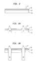
- FIG. 1A is a schematic diagram of a conventional four-by-four array of dynamic random access (DRAM) cells.
- DRAM dynamic random access
- This conventional array can be rearranged to the shared-gate, double-bit array shown in Figure lB.
- This latter array layout can be implemented with a vertical gate FET described in the aforementioned co-pending application. It also allows both bit and substrate contacts to be shared by adjacent cells.
- the state of the art in DRAM technology continuously seeks to increase the cell density per integrated circuit chip. This requires small feature size, preferably using conventional photolithography process steps, and efficient use of the semiconductor chip area.
- An object of this invention is the provision of a high-density DRAM structure using a silicon-on-oxide wafer and conventional photolithographic process steps; a DRAM with a cell area on the order of three to four times the feature size (e.g., 1.5 ⁇ m2 to 2.0 ⁇ m2 cell area with a 0.5 ⁇ m feature size).
- Another object of the invention is a DRAM cell that is relatively immune to soft errors that are caused by alpha particle and cosmic ray irradiation.
- a further object of the invention is a DRAM structure where both the bit and substrate contacts are shared by adjacent cells.
- Another object of the invention is to reduce bit-line capacitance by using the SOI wafer to improve DRAM speed. Furthermore, the use of a stacked capacitor in the trench, with its node plate uniquely connected to the device substrate, can greatly reduce trench capacitor leakage problems and result in longer charge-retention time.
- this invention contemplates the provision of a high density, DRAM cell array that can be manufactured using conventional photolithography process steps.
- the conventional four-by-four DRAM array shown schematically in Figure 1a can be rearranged to the shared-gate, double-bit array shown schematically in Figure lb.
- Stacked trench storage capacitors and vertical FET transistors are arranged in pairs with a common vertical gate and a common substrate, allowing both bit and substrate contacts to be shared by adjacent cells.
- FIGS 1a and 1b are schematic drawings of DRAM cell arrays.
- FIGS. 2 through 2K are sectional views of a cell in accordance with the teachings of this invention at various illustrative process stages.
- Figures 3 and 4 are schematic drawings of finished DRAM cells for both cross-sectional and plan view, respectively.
- the preferred starting point is a silicon- on-oxide wafer with an oxide layer 10, a thin silicon layer 12 supported by a semiconductor wafer (not shown).
- the silicon layer 12 is n doped.
- a layer 16 of thermal oxide 1000 ⁇ thick is grown over the silicon surface, and a nitride layer 17 about 2000 ⁇ thick is deposited on the surface of the oxide layer.
- a pattern of a trench used for cell capacitor is formed in a photo-resist (not shown) with a suitable lithography tool; the trench width is on the order of 0.8 ⁇ m (the dimension picked here is for an arbitrary design ground rule).
- the oxide/nitride layer 16, the silicon layer 12, and the oxide layer 10 are then etched to form openings 18, stopping at the surface of support wafer.
- the resist is then stripped.
- a nitride spacer 20, about 800 ⁇ thick, is formed by a blanket deposited CVD nitride layer followed by reactive ion etching to leave only the spacer 20 on the sidewalls.
- the device after this reactive ion etch step is shown in Figure 2A.
- trenches 22 are etched into the support wafer to a depth of about 0.5 ⁇ m by a reactive ion etching step using a Cl2/O2 plasma.
- the etch rate of silicon is greater than ten times than the etch rate of silicon oxide and silicon nitride.
- a trench with these dimensions provides a capacitance on the order of 40 fF.
- a layer of thermal oxide 24 about 1500 A thick is grown on the trench sidewalls after they have been cleaned.
- the silicon layer 12 is covered by nitride spacer 20 and is not oxidized in this step as shown in Figure 2Bb.
- Figure 2Bc shows the trench wall at this step.
- a layer 30 of n+ doped polysilicon is deposited, lithographically patterned, and etched to form the capacitor node electrode.
- the layer 30 is connected to the silicon layer 12, which will become the source layer of the completed FET device.
- In situ doped polysilicon as well as ion implanted silicon can be used for layer 30.
- a composite capacitor oxidenitride-oxide layer 32 is formed using a conventional technique (about 70 ⁇ ).
- Figure 2Bd shows a detail of the trench SOI area at this stage, and Figure 2C shows the larger structure at this same state.
- the silicon layer 12 is then patterned, and etched in the regions indicated by the general reference numeral 38, to form silicon islands upon which FET pairs are formed. Grow high-pressure-oxide 12A to seal the edge of the exposed silicon regions.
- the oxide layer 16 is opened in the central region 39 between two trench capacitors where the vertical gate will be formed, and a layer 40 of n+ doped epitaxial silicon is, preferably by a low temperature epitaxial process.
- the layer 40 can be formed by recrystallizing deposited in situ doped amorphous silicon.
- layer 40 can be formed by a lateral overgrowth epitaxial process. This layer 40, which covers the upper surfaces and trench walls of the device, serves both as a substrate plate electrode for the capacitor and as a channel layer in the completed device. The device at this state is shown in Figure 2E and in fragmentary detail of the left corner of the trench capacitor in Figure 2Ea.
- a CVD oxide layer 42 is deposited, patterned to open the central gate region 39, and the patterned region opened.
- the device at this state is shown in Figure 2F.
- the device in this state is shown in Figure 2G.
- the oxide layer 46 is patterned, and an opening, indicated by the general reference numeral 48 in Figure 2H, is etched through all the layers extending to the top surface of SOI burned oxide layer 10.
- a gate oxide 49 is grown as a thin oxide (about 65 ⁇ , for example) on the wall of the opening 48.
- gate stack material is attached to define the gate, the sidewalls 53 of the exposed gate structure are oxidized by a HIPOX process step. The structure of the completion of these process steps is shown in Figure 2I.
- An ion implant step is performed at this stage to dope the gate and drain polysilicon regions with arsenic.
- a block-out resist 55 is applied and patterned, to define a drain contact area (which in the final DRAM cell is a bit-line contact), followed by a ion implant to dope the substrate area with boron to reduce substrate contact resistance. This step is illustrated in Figure 2J.
- the resist 55 is removed and the exposed silicon walls oxidized (59) by a HIPOX step.
- the substrate layer is common to all the cells, it is not necessary to have a contact to each cell. It can be arranged to make one substrate contact per every 128 bits (for example).
- source and substrate contact regions are formed, the structure is covered with a suitable dielectric 57, openings are made in the dielectric, contacts are formed in the dielectric and the upper surface is planarized.
- the completed structure is shown in Figure 2K.
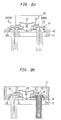
- FIG. 3 A cross-sectional view of a four-cell DRAM array is shown in Figure 3 with a shared bit contact.
- Figure 4 is a plan view of an exemplary layout for the cell array. As shown in Figure 4, the word lines, polysilicon gate, are running in a vertical direction while bit lines, mostly metal, such as CVD tungsten, run in a horizontal direction. A suitable contact line is necessary for only every 128 cells. The dotted line indicates a single cell.
Abstract
A high density, DRAM cell array with a very short channel, vertical gate transfer transistor that can be manufactured using conventional photolithography process steps. The conventional four-by-four DRAM array shown schematically in Figure 1a is rearranged to the shared-gate, double-bit array shown schematically in Figure 1b. Trench storage capacitors and vertical FET transistors are arranged in pairs with a common vertical gate and a common substrate, allowing both bit and substrate contacts to be shared by adjacent cells.
The polysilicon layer (40) serves both as a substrate plate electrode for the capacitor and as a channel layer for the vertical transfer transistor with gate (50).
Description
- This invention relates to an improved semiconductor structure for high-density, dynamic random access memory (DRAM) arrays, and more particularly, to a structure that can be implemented with a small feature size and is efficient in area utilization.
- This application is related to European patent application, filed on the same day, entitled "Vertical Gate Transistor With Low Temperature Epitaxial Channel" and assigned to the assignee of this application, and the description of which being hereinafter enclosed.
- Because the conventional planar capacitor cell cannot achieve sufficient storage capacitance, various three-dimensional cell structures have been proposed in the prior art for producing mega-bit DRAMs. Cells using trench capacitors have been proposed in order to maintain sufficient storage capacitance. An article entitled "A New Soft-Error Immune DRAM Cell With a Transistor On a Lateral Epitaxial Silicon Layer (Tole Cell)", by T. Kubota et al., IEEE Journal, 1987, pgs. 344-347, discloses a DRAM cell with trench capacitors. This cell is produced by a silicon-on-insulator fabrication technology that combines epitaxial lateral overgrowth and preferential polishing to produce a cell with a conventional gate structure for each cell.
- Figure 1A is a schematic diagram of a conventional four-by-four array of dynamic random access (DRAM) cells.
- This conventional array can be rearranged to the shared-gate, double-bit array shown in Figure lB. This latter array layout can be implemented with a vertical gate FET described in the aforementioned co-pending application. It also allows both bit and substrate contacts to be shared by adjacent cells. In an effort to reduce the cost per memory cell, the state of the art in DRAM technology continuously seeks to increase the cell density per integrated circuit chip. This requires small feature size, preferably using conventional photolithography process steps, and efficient use of the semiconductor chip area.
- An object of this invention is the provision of a high-density DRAM structure using a silicon-on-oxide wafer and conventional photolithographic process steps; a DRAM with a cell area on the order of three to four times the feature size (e.g., 1.5µm² to 2.0 µm² cell area with a 0.5 µm feature size).
- Another object of the invention is a DRAM cell that is relatively immune to soft errors that are caused by alpha particle and cosmic ray irradiation.
- A further object of the invention is a DRAM structure where both the bit and substrate contacts are shared by adjacent cells.
- Another object of the invention is to reduce bit-line capacitance by using the SOI wafer to improve DRAM speed. Furthermore, the use of a stacked capacitor in the trench, with its node plate uniquely connected to the device substrate, can greatly reduce trench capacitor leakage problems and result in longer charge-retention time.
- Briefly, this invention contemplates the provision of a high density, DRAM cell array that can be manufactured using conventional photolithography process steps. The conventional four-by-four DRAM array shown schematically in Figure 1a can be rearranged to the shared-gate, double-bit array shown schematically in Figure lb. Stacked trench storage capacitors and vertical FET transistors are arranged in pairs with a common vertical gate and a common substrate, allowing both bit and substrate contacts to be shared by adjacent cells.
- The foregoing and other objects, aspects and advantages will be better understood from the following detailed description of a preferred embodiment of the invention with reference to the drawings, in which:
- Figures 1a and 1b are schematic drawings of DRAM cell arrays.
- Figures 2 through 2K are sectional views of a cell in accordance with the teachings of this invention at various illustrative process stages.
- Figures 3 and 4 are schematic drawings of finished DRAM cells for both cross-sectional and plan view, respectively.
- Referring now to the drawings, starting with Figure 2, the preferred starting point is a silicon- on-oxide wafer with an
oxide layer 10, athin silicon layer 12 supported by a semiconductor wafer (not shown). In this exemplary embodiment of the invention thesilicon layer 12 is n doped. Alayer 16 of thermal oxide 1000 Å thick is grown over the silicon surface, and anitride layer 17 about 2000 Å thick is deposited on the surface of the oxide layer. It should be noted that in the following Figures, some reference numerals that are repeated from one Figure to the next have been omitted in some of the Figures subsequent to their first introduction for the purposes of visual clarity. - Referring now to Figure 2A, a pattern of a trench used for cell capacitor is formed in a photo-resist (not shown) with a suitable lithography tool; the trench width is on the order of 0.8 µm (the dimension picked here is for an arbitrary design ground rule). The oxide/
nitride layer 16, thesilicon layer 12, and theoxide layer 10 are then etched to formopenings 18, stopping at the surface of support wafer. The resist is then stripped. Anitride spacer 20, about 800 Å thick, is formed by a blanket deposited CVD nitride layer followed by reactive ion etching to leave only thespacer 20 on the sidewalls. The device after this reactive ion etch step is shown in Figure 2A. - Next,
trenches 22 are etched into the support wafer to a depth of about 0.5 µm by a reactive ion etching step using a Cl₂/O₂ plasma. Here, it should be noted that the etch rate of silicon is greater than ten times than the etch rate of silicon oxide and silicon nitride. A trench with these dimensions provides a capacitance on the order of 40 fF. - Referring now to the enlarged fragmentary drawings 2Ba through 2Bd. The left-hand side of one of the trench wall areas is shown in the enlarged view of Figure 2Ba.
- To provide a DRAM structure with an immunity to alpha particle radiation, and also to reduce leakage of storage charges, a layer of
thermal oxide 24 about 1500 A thick is grown on the trench sidewalls after they have been cleaned. Thesilicon layer 12 is covered bynitride spacer 20 and is not oxidized in this step as shown in Figure 2Bb. - The
nitride spacer 20 is then stripped in a hot solution of H₃PO₄. Figure 2Bc shows the trench wall at this step. - Next, a
layer 30 of n+ doped polysilicon is deposited, lithographically patterned, and etched to form the capacitor node electrode. Here it should be noted that thelayer 30 is connected to thesilicon layer 12, which will become the source layer of the completed FET device. In situ doped polysilicon as well as ion implanted silicon can be used forlayer 30. A composite capacitor oxidenitride-oxide layer 32 is formed using a conventional technique (about 70 Å). Figure 2Bd shows a detail of the trench SOI area at this stage, and Figure 2C shows the larger structure at this same state. - As can best be seen with reference to Figure 2D, the
silicon layer 12 is then patterned, and etched in the regions indicated by thegeneral reference numeral 38, to form silicon islands upon which FET pairs are formed. Grow high-pressure-oxide 12A to seal the edge of the exposed silicon regions. - The
oxide layer 16 is opened in thecentral region 39 between two trench capacitors where the vertical gate will be formed, and alayer 40 of n+ doped epitaxial silicon is, preferably by a low temperature epitaxial process. Alternatively, thelayer 40 can be formed by recrystallizing deposited in situ doped amorphous silicon. Also,layer 40 can be formed by a lateral overgrowth epitaxial process. Thislayer 40, which covers the upper surfaces and trench walls of the device, serves both as a substrate plate electrode for the capacitor and as a channel layer in the completed device. The device at this state is shown in Figure 2E and in fragmentary detail of the left corner of the trench capacitor in Figure 2Ea. - Next, a
CVD oxide layer 42 is deposited, patterned to open thecentral gate region 39, and the patterned region opened. The device at this state is shown in Figure 2F. ACVD layer 44 of n-type polysilicon, to form the drain, is then conformally deposited and anoxide layer 46 is grown on its surface. The device in this state is shown in Figure 2G. - The
oxide layer 46 is patterned, and an opening, indicated by thegeneral reference numeral 48 in Figure 2H, is etched through all the layers extending to the top surface of SOI burnedoxide layer 10. Agate oxide 49 is grown as a thin oxide (about 65 Å, for example) on the wall of the opening 48. - A
gate stack 50 including a CVD deposit of n+ polysilicon, filling theopening 48 and extending up over theoxide layer 46, a thin oxide layer grows over the polysilicon and athin nitride layer 52 is formed using conventional process steps. After gate stack material is attached to define the gate, thesidewalls 53 of the exposed gate structure are oxidized by a HIPOX process step. The structure of the completion of these process steps is shown in Figure 2I. An ion implant step is performed at this stage to dope the gate and drain polysilicon regions with arsenic. A block-out resist 55 is applied and patterned, to define a drain contact area (which in the final DRAM cell is a bit-line contact), followed by a ion implant to dope the substrate area with boron to reduce substrate contact resistance. This step is illustrated in Figure 2J. The resist 55 is removed and the exposed silicon walls oxidized (59) by a HIPOX step. - Since the substrate layer is common to all the cells, it is not necessary to have a contact to each cell. It can be arranged to make one substrate contact per every 128 bits (for example).
- Using conventional process steps such as those described in more detail in the above-referenced co-pending application, source and substrate contact regions are formed, the structure is covered with a
suitable dielectric 57, openings are made in the dielectric, contacts are formed in the dielectric and the upper surface is planarized. The completed structure is shown in Figure 2K. - A cross-sectional view of a four-cell DRAM array is shown in Figure 3 with a shared bit contact. Figure 4 is a plan view of an exemplary layout for the cell array. As shown in Figure 4, the word lines, polysilicon gate, are running in a vertical direction while bit lines, mostly metal, such as CVD tungsten, run in a horizontal direction. A suitable contact line is necessary for only every 128 cells. The dotted line indicates a single cell.
Claims (13)
- An integrated circuit cell for dynamic random access memories, comprising in combination:
a silicon-on-oxide wafer comprised of an oxide layer on the upper surface of an underlying support wafer and a silicon source layer on the upper surface of said oxide layer;
a capacitor trench extending through said silicon source layer and said oxide layer and into said underlying support wafer;
a first capacitor plate layer formed conformally on the wall of said capacitor trench, said capacitor plate layer extending to and connected with said silicon source layer;
a capacitor dielectric layer formed on said polysilicon capacitor plate layer;
a silicon channel layer formed conformally over said capacitor dielectric layer and overlying a region of said patterned silicon source layer, said silicon channel layer forming a second capacitor plate and as well as a channel layer;
a polysilicon drain layer overlying said silicon channel layer in said region where said silicon channel layer overlays said silicon source layer;
a vertical opening extending through silicon source layer, said silicon channel layer, and said polysilicon drain layer forming a wall surface in the region where the layers overlay one another with an edge in each layer respectively aligned vertically along said wall surface;
a gate dielectric covering said wall surface; and
a vertical gate in said opening in contact with said gate dielectric. - An integrated circuit cell for dynamic random access memories as in claim 1, further including an isolation dielectric layer formed on the wall of said capacitor trench.
- An integrated circuit cell for dynamic random access memories as in claim 1, wherein said capacitor dielectric layer is an oxide-nitride composite.
- As integrated circuit cell for dynamic random access memories as in claim 1, wherein said capacitor dielectric layer is an oxide.
- An integrated circuit cell for dynamic random access memories as in claim 1, wherein said gate dielectric is an oxide-nitride composite.
- An integrated circuit cell for dynamic random access memories as in claim 1, wherein said gate dielectric is an oxide.
- An integrated circuit cell for dynamic random access memories as in claim 1, further including:
a substrate contract region in said epitaxial silicon layer; and
a bit-line contact region in said polysilicon drain layer. - An integrated circuit cell for dynamic random access memories as in claim 1, wherein said silicon channel layer is a low temperature epitaxially grown layer.
- An integrated circuit cell for dynamic random access memories as in claim 1, wherein said silicon channel is a solid-phase recrystallized amorphous silicon.
- A pair of integrated circuit, shared gate, cells for dynamic random access memories, comprising in combination:
a silicon-on-oxide wafer comprised of an oxide layer on the upper surface of an underlying support wafer and a silicon source layer on the upper surface of said oxide layer;
a pair of capacitor trenches extending through said silicon source layer and said oxide layer and into said underlying support wafer;
a first capacitor plate layer formed conformally on the wall of each of said pair of said capacitor trenches over said isolation oxide, said capacitor plate layer extending to and connected with said silicon source layer;
a capacitor dielectric layer formed on said polysilicon capacitor plate layer;
a silicon channel layer formed conformally over said capacitor dielectric layer and overlying a region of said silicon source layer, said silicon layer forming a second capacitor plate and a channel layer;
a polysilicon drain layer overlying said silicon channel layer in said region where said silicon channel layer overlays said silicon source layer;
a vertical opening extending through silicon source layer, said silicon channel layer, and said polysilicon drain layer forming a pair of facing vertical wall surfaces in the region where the layers overlay one another with an edge in each layer respectively aligned vertically along said pair of facing vertical wall surfaces;
said silicon channel layer extending from one of said facing wall surfaces forming the channel layer and the second capacitor plate layer for one cell of said pair of integrated circuit cells and said silicon channel layer extending from the other of said facing wall surfaces forming the channel layer and the second capacitor plate layer for the other cell of said pair of integrated circuit cells;
a gate dielectric covering said pair of facing vertical wall surfaces; and
a vertical gate in said opening in contact with said gate dielectric. - A pair of integrated circuit, shared gate, cells for dynamic random access memories as in claim 10, further including:
a substrate contact region in said silicon channel layer common to said pair of integrated circuit cells; and
a bit-line contact region in said polysilicon drain layer extending from said one of said facing wall surfaces. - A method of forming an integrated circuit cell for dynamic random access memories, comprising the steps of:
patterning a silicon source layer on a silicon-on-oxide wafer comprised of an oxide layer on the upper surface of an underlying support wafer;
etching a capacitor trench that extends through said patterned silicon source layer and said oxide layer and into said underlying support wafer;
conformally depositing a first capacitor plate layer on the wall of said capacitor trench, said first capacitor plate layer extending to and connected with said silicon source layer;
forming a capacitor dielectric layer on said first capacitor plate layer;
conformally forming an silicon channel layer over said capacitor dielectric layer and overlying a region of said silicon channel layer, said silicon channel layer forming a second capacitor plate and a channel layer;
depositing a polysilicon drain layer overlying said silicon channel layer in said region where said silicon channel layer overlays said silicon source layer;
etching a vertical opening extending through silicon source layer, said silicon channel layer, and said polysilicon drain layer, said vertical opening forming a wall surface in the region where the layers overlay one another with an edge in each layer respectively aligned vertically along said wall surface;
forming a gate dielectric covering said wall surface; and
forming a vertical gate in said opening in contact with said gate dielectric. - A method of forming a pair of integrated circuit, shared gate, cells for dynamic random access memories, comprising in combination:
patterning a silicon-on-oxide wafer comprised of an oxide layer on the upper surface of an underlying support wafer;
etching a pair of capacitor trenches that extend through said patterned silicon source layer and said oxide layer and into said underlying support wafer;
conformally depositing a first capacitor plate layer on the wall of each of said pair of said capacitor trenches, said first capacitor plate layer extending to and connected with said silicon source layer;
forming a capacitor dielectric layer on said polysilicon capacitor plate layer;
forming an silicon channel layer conformally over said capacitor dielectric layer and overlying a region of said silicon source layer, said silicon channel layer forming a second capacitor plate and a channel layer;
forming a polysilicon drain layer overlying said silicon channel layer in said region where said silicon channel layer overlays said silicon layer;
etching a vertical opening extending through silicon source layer, said silicon channel layer, and said polysilicon drain layer forming a pair of facing vertical wall surfaces in the region where the layers overlay one another with an edge in each layer respectively aligned vertically along said pair of facing vertical wall surfaces, said silicon channel layer extending from one of said facing wall surfaces forming the channel layer and the second capacitor plate layer for one cell of said pair of integrated circuit cells and said silicon channel layer extending from the other of said facing wall surfaces forming the channel layer and the second capacitor plate layer for the other cell of said pair of integrated circuit cells;
forming a gate dielectric covering said pair of facing vertical wall surfaces; and
forming a vertical gate in said opening in contact with said gate dielectric.
Applications Claiming Priority (2)
| Application Number | Priority Date | Filing Date | Title |
|---|---|---|---|
| US900041 | 1992-06-17 | ||
| US07/900,041 US5528062A (en) | 1992-06-17 | 1992-06-17 | High-density DRAM structure on soi |
Publications (2)
| Publication Number | Publication Date |
|---|---|
| EP0579566A2 true EP0579566A2 (en) | 1994-01-19 |
| EP0579566A3 EP0579566A3 (en) | 1995-08-09 |
Family
ID=25411894
Family Applications (1)
| Application Number | Title | Priority Date | Filing Date |
|---|---|---|---|
| EP93480054A Withdrawn EP0579566A3 (en) | 1992-06-17 | 1993-05-05 | High-density dram structure on SOI. |
Country Status (3)
| Country | Link |
|---|---|
| US (2) | US5528062A (en) |
| EP (1) | EP0579566A3 (en) |
| JP (1) | JPH0799770B2 (en) |
Cited By (22)
| Publication number | Priority date | Publication date | Assignee | Title |
|---|---|---|---|---|
| US6310375B1 (en) * | 1998-04-06 | 2001-10-30 | Siemens Aktiengesellschaft | Trench capacitor with isolation collar and corresponding manufacturing method |
| US6417064B1 (en) * | 2001-03-09 | 2002-07-09 | Nanya Technology Corporation | Method for treating the surface of a deep trench |
| US7732816B2 (en) | 2001-06-18 | 2010-06-08 | Innovative Silicon Isi Sa | Semiconductor device |
| US7736959B2 (en) | 2003-07-22 | 2010-06-15 | Innovative Silicon Isi Sa | Integrated circuit device, and method of fabricating same |
| US8861247B2 (en) | 2009-04-27 | 2014-10-14 | Micron Technology, Inc. | Techniques for providing a direct injection semiconductor memory device |
| US8947965B2 (en) | 2009-07-27 | 2015-02-03 | Micron Technology Inc. | Techniques for providing a direct injection semiconductor memory device |
| US8964479B2 (en) | 2010-03-04 | 2015-02-24 | Micron Technology, Inc. | Techniques for sensing a semiconductor memory device |
| US8982633B2 (en) | 2009-05-22 | 2015-03-17 | Micron Technology, Inc. | Techniques for providing a direct injection semiconductor memory device |
| US9019788B2 (en) | 2008-01-24 | 2015-04-28 | Micron Technology, Inc. | Techniques for accessing memory cells |
| US9019759B2 (en) | 2010-03-15 | 2015-04-28 | Micron Technology, Inc. | Techniques for providing a semiconductor memory device |
| US9064730B2 (en) | 2009-03-04 | 2015-06-23 | Micron Technology, Inc. | Techniques for forming a contact to a buried diffusion layer in a semiconductor memory device |
| US9093311B2 (en) | 2009-03-31 | 2015-07-28 | Micron Technology, Inc. | Techniques for providing a semiconductor memory device |
| US9142264B2 (en) | 2010-05-06 | 2015-09-22 | Micron Technology, Inc. | Techniques for refreshing a semiconductor memory device |
| US9240496B2 (en) | 2009-04-30 | 2016-01-19 | Micron Technology, Inc. | Semiconductor device with floating gate and electrically floating body |
| US9257155B2 (en) | 2007-05-30 | 2016-02-09 | Micron Technology, Inc. | Integrated circuit having voltage generation circuitry for memory cell array, and method of operating and/or controlling same |
| US9263133B2 (en) | 2011-05-17 | 2016-02-16 | Micron Technology, Inc. | Techniques for providing a semiconductor memory device |
| US9276000B2 (en) | 2007-03-29 | 2016-03-01 | Micron Technology, Inc. | Manufacturing process for zero-capacitor random access memory circuits |
| US9331083B2 (en) | 2009-07-10 | 2016-05-03 | Micron Technology, Inc. | Techniques for providing a semiconductor memory device |
| US9553186B2 (en) | 2008-09-25 | 2017-01-24 | Micron Technology, Inc. | Recessed gate silicon-on-insulator floating body device with self-aligned lateral isolation |
| US9812179B2 (en) | 2009-11-24 | 2017-11-07 | Ovonyx Memory Technology, Llc | Techniques for reducing disturbance in a semiconductor memory device |
| US10304837B2 (en) | 2007-11-29 | 2019-05-28 | Ovonyx Memory Technology, Llc | Integrated circuit having memory cell array including barriers, and method of manufacturing same |
| US10418091B2 (en) | 2005-09-07 | 2019-09-17 | Ovonyx Memory Technology, Llc | Memory cell and memory cell array having an electrically floating body transistor, and methods of operating same |
Families Citing this family (110)
| Publication number | Priority date | Publication date | Assignee | Title |
|---|---|---|---|---|
| DE69333551T2 (en) * | 1993-02-04 | 2005-06-23 | Cornell Research Foundation, Inc. | Single mask process for making microstructures, single crystal fabrication process |
| JP3304635B2 (en) | 1994-09-26 | 2002-07-22 | 三菱電機株式会社 | Semiconductor storage device |
| DE4442976A1 (en) * | 1994-12-02 | 1996-06-05 | Thomson Brandt Gmbh | Device for the contactless optical scanning of information when recording on and / or playing back from a recording medium with recording tracks |
| US6740573B2 (en) | 1995-02-17 | 2004-05-25 | Micron Technology, Inc. | Method for forming an integrated circuit interconnect using a dual poly process |
| US5658816A (en) * | 1995-02-27 | 1997-08-19 | International Business Machines Corporation | Method of making DRAM cell with trench under device for 256 Mb DRAM and beyond |
| US5606188A (en) * | 1995-04-26 | 1997-02-25 | International Business Machines Corporation | Fabrication process and structure for a contacted-body silicon-on-insulator dynamic random access memory |
| US5872733A (en) * | 1995-06-06 | 1999-02-16 | International Business Machines Corporation | Ramp-up rate control circuit for flash memory charge pump |
| US5585285A (en) * | 1995-12-06 | 1996-12-17 | Micron Technology, Inc. | Method of forming dynamic random access memory circuitry using SOI and isolation trenches |
| US5929476A (en) * | 1996-06-21 | 1999-07-27 | Prall; Kirk | Semiconductor-on-insulator transistor and memory circuitry employing semiconductor-on-insulator transistors |
| US5811283A (en) * | 1996-08-13 | 1998-09-22 | United Microelectronics Corporation | Silicon on insulator (SOI) dram cell structure and process |
| US5691230A (en) * | 1996-09-04 | 1997-11-25 | Micron Technology, Inc. | Technique for producing small islands of silicon on insulator |
| US5770875A (en) * | 1996-09-16 | 1998-06-23 | International Business Machines Corporation | Large value capacitor for SOI |
| US5846888A (en) * | 1996-09-27 | 1998-12-08 | Micron Technology, Inc. | Method for in-situ incorporation of desirable impurities into high pressure oxides |
| US5770484A (en) * | 1996-12-13 | 1998-06-23 | International Business Machines Corporation | Method of making silicon on insulator buried plate trench capacitor |
| US6160292A (en) * | 1997-04-23 | 2000-12-12 | International Business Machines Corporation | Circuit and methods to improve the operation of SOI devices |
| US6133608A (en) * | 1997-04-23 | 2000-10-17 | International Business Machines Corporation | SOI-body selective link method and apparatus |
| US5998821A (en) * | 1997-05-21 | 1999-12-07 | Kabushiki Kaisha Toshiba | Dynamic ram structure having a trench capacitor |
| US6191470B1 (en) | 1997-07-08 | 2001-02-20 | Micron Technology, Inc. | Semiconductor-on-insulator memory cell with buried word and body lines |
| US6150687A (en) | 1997-07-08 | 2000-11-21 | Micron Technology, Inc. | Memory cell having a vertical transistor with buried source/drain and dual gates |
| US5936274A (en) * | 1997-07-08 | 1999-08-10 | Micron Technology, Inc. | High density flash memory |
| US6072209A (en) * | 1997-07-08 | 2000-06-06 | Micro Technology, Inc. | Four F2 folded bit line DRAM cell structure having buried bit and word lines |
| US5973356A (en) * | 1997-07-08 | 1999-10-26 | Micron Technology, Inc. | Ultra high density flash memory |
| US5909618A (en) * | 1997-07-08 | 1999-06-01 | Micron Technology, Inc. | Method of making memory cell with vertical transistor and buried word and body lines |
| US5914511A (en) * | 1997-10-06 | 1999-06-22 | Micron Technology, Inc. | Circuit and method for a folded bit line memory using trench plate capacitor cells with body bias contacts |
| US6066869A (en) | 1997-10-06 | 2000-05-23 | Micron Technology, Inc. | Circuit and method for a folded bit line memory cell with vertical transistor and trench capacitor |
| US5907170A (en) * | 1997-10-06 | 1999-05-25 | Micron Technology, Inc. | Circuit and method for an open bit line memory cell with a vertical transistor and trench plate trench capacitor |
| US6528837B2 (en) | 1997-10-06 | 2003-03-04 | Micron Technology, Inc. | Circuit and method for an open bit line memory cell with a vertical transistor and trench plate trench capacitor |
| US6069390A (en) | 1998-01-15 | 2000-05-30 | International Business Machines Corporation | Semiconductor integrated circuits with mesas |
| US6177299B1 (en) | 1998-01-15 | 2001-01-23 | International Business Machines Corporation | Transistor having substantially isolated body and method of making the same |
| US6025225A (en) * | 1998-01-22 | 2000-02-15 | Micron Technology, Inc. | Circuits with a trench capacitor having micro-roughened semiconductor surfaces and methods for forming the same |
| US6242775B1 (en) | 1998-02-24 | 2001-06-05 | Micron Technology, Inc. | Circuits and methods using vertical complementary transistors |
| US6246083B1 (en) | 1998-02-24 | 2001-06-12 | Micron Technology, Inc. | Vertical gain cell and array for a dynamic random access memory |
| US5963469A (en) * | 1998-02-24 | 1999-10-05 | Micron Technology, Inc. | Vertical bipolar read access for low voltage memory cell |
| US6304483B1 (en) | 1998-02-24 | 2001-10-16 | Micron Technology, Inc. | Circuits and methods for a static random access memory using vertical transistors |
| US6448615B1 (en) | 1998-02-26 | 2002-09-10 | Micron Technology, Inc. | Methods, structures, and circuits for transistors with gate-to-body capacitive coupling |
| US5991225A (en) * | 1998-02-27 | 1999-11-23 | Micron Technology, Inc. | Programmable memory address decode array with vertical transistors |
| US6124729A (en) * | 1998-02-27 | 2000-09-26 | Micron Technology, Inc. | Field programmable logic arrays with vertical transistors |
| US6307235B1 (en) | 1998-03-30 | 2001-10-23 | Micron Technology, Inc. | Another technique for gated lateral bipolar transistors |
| US6229342B1 (en) | 1998-03-30 | 2001-05-08 | Micron Technology, Inc. | Circuits and method for body contacted and backgated transistors |
| US6049496A (en) * | 1998-03-30 | 2000-04-11 | Micron Technology, Inc. | Circuit and method for low voltage, current sense amplifier |
| US6104066A (en) * | 1998-03-30 | 2000-08-15 | Micron Technology, Inc. | Circuit and method for low voltage, voltage sense amplifier |
| US6107663A (en) * | 1998-03-30 | 2000-08-22 | Micron Technology, Inc. | Circuit and method for gate-body structures in CMOS technology |
| US6097065A (en) | 1998-03-30 | 2000-08-01 | Micron Technology, Inc. | Circuits and methods for dual-gated transistors |
| US6075272A (en) * | 1998-03-30 | 2000-06-13 | Micron Technology, Inc. | Structure for gated lateral bipolar transistors |
| US6043527A (en) * | 1998-04-14 | 2000-03-28 | Micron Technology, Inc. | Circuits and methods for a memory cell with a trench plate trench capacitor and a vertical bipolar read device |
| US6410369B1 (en) | 1998-04-22 | 2002-06-25 | International Business Machines Corporation | Soi-body selective link method and apparatus |
| US6097056A (en) * | 1998-04-28 | 2000-08-01 | International Business Machines Corporation | Field effect transistor having a floating gate |
| US6134175A (en) | 1998-08-04 | 2000-10-17 | Micron Technology, Inc. | Memory address decode array with vertical transistors |
| US6208164B1 (en) | 1998-08-04 | 2001-03-27 | Micron Technology, Inc. | Programmable logic array with vertical transistors |
| US6093623A (en) * | 1998-08-04 | 2000-07-25 | Micron Technology, Inc. | Methods for making silicon-on-insulator structures |
| US6423613B1 (en) | 1998-11-10 | 2002-07-23 | Micron Technology, Inc. | Low temperature silicon wafer bond process with bulk material bond strength |
| US6188122B1 (en) | 1999-01-14 | 2001-02-13 | International Business Machines Corporation | Buried capacitor for silicon-on-insulator structure |
| US6690038B1 (en) | 1999-06-05 | 2004-02-10 | T-Ram, Inc. | Thyristor-based device over substrate surface |
| US6153902A (en) * | 1999-08-16 | 2000-11-28 | International Business Machines Corporation | Vertical DRAM cell with wordline self-aligned to storage trench |
| US6500744B2 (en) | 1999-09-02 | 2002-12-31 | Micron Technology, Inc. | Methods of forming DRAM assemblies, transistor devices, and openings in substrates |
| US6387772B1 (en) | 2000-04-25 | 2002-05-14 | Agere Systems Guardian Corp. | Method for forming trench capacitors in SOI substrates |
| US6396121B1 (en) * | 2000-05-31 | 2002-05-28 | International Business Machines Corporation | Structures and methods of anti-fuse formation in SOI |
| US6583462B1 (en) | 2000-10-31 | 2003-06-24 | International Business Machines Corporation | Vertical DRAM having metallic node conductor |
| US6570207B2 (en) | 2000-12-13 | 2003-05-27 | International Business Machines Corporation | Structure and method for creating vertical capacitor and anti-fuse in DRAM process employing vertical array device cell complex |
| US6852167B2 (en) | 2001-03-01 | 2005-02-08 | Micron Technology, Inc. | Methods, systems, and apparatus for uniform chemical-vapor depositions |
| US7456439B1 (en) | 2001-03-22 | 2008-11-25 | T-Ram Semiconductor, Inc. | Vertical thyristor-based memory with trench isolation and its method of fabrication |
| US7374974B1 (en) | 2001-03-22 | 2008-05-20 | T-Ram Semiconductor, Inc. | Thyristor-based device with trench dielectric material |
| US6727528B1 (en) | 2001-03-22 | 2004-04-27 | T-Ram, Inc. | Thyristor-based device including trench dielectric isolation for thyristor-body regions |
| EP1355316B1 (en) * | 2002-04-18 | 2007-02-21 | Innovative Silicon SA | Data storage device and refreshing method for use with such device |
| EP1357603A3 (en) | 2002-04-18 | 2004-01-14 | Innovative Silicon SA | Semiconductor device |
| US7160577B2 (en) | 2002-05-02 | 2007-01-09 | Micron Technology, Inc. | Methods for atomic-layer deposition of aluminum oxides in integrated circuits |
| US7589029B2 (en) | 2002-05-02 | 2009-09-15 | Micron Technology, Inc. | Atomic layer deposition and conversion |
| US6756612B1 (en) | 2002-10-28 | 2004-06-29 | T-Ram, Inc. | Carrier coupler for thyristor-based semiconductor device |
| US6965129B1 (en) | 2002-11-06 | 2005-11-15 | T-Ram, Inc. | Thyristor-based device having dual control ports |
| US7085153B2 (en) * | 2003-05-13 | 2006-08-01 | Innovative Silicon S.A. | Semiconductor memory cell, array, architecture and device, and method of operating same |
| US20040228168A1 (en) * | 2003-05-13 | 2004-11-18 | Richard Ferrant | Semiconductor memory device and method of operating same |
| US6912150B2 (en) * | 2003-05-13 | 2005-06-28 | Lionel Portman | Reference current generator, and method of programming, adjusting and/or operating same |
| US7184298B2 (en) * | 2003-09-24 | 2007-02-27 | Innovative Silicon S.A. | Low power programming technique for a floating body memory transistor, memory cell, and memory array |
| US7476939B2 (en) * | 2004-11-04 | 2009-01-13 | Innovative Silicon Isi Sa | Memory cell having an electrically floating body transistor and programming technique therefor |
| US7251164B2 (en) * | 2004-11-10 | 2007-07-31 | Innovative Silicon S.A. | Circuitry for and method of improving statistical distribution of integrated circuits |
| FR2879344B1 (en) * | 2004-12-10 | 2007-03-16 | St Microelectronics Sa | REALIZATION OF INTEGRATED CAPACITOR |
| US7301838B2 (en) * | 2004-12-13 | 2007-11-27 | Innovative Silicon S.A. | Sense amplifier circuitry and architecture to write data into and/or read from memory cells |
| US7301803B2 (en) * | 2004-12-22 | 2007-11-27 | Innovative Silicon S.A. | Bipolar reading technique for a memory cell having an electrically floating body transistor |
| US7927948B2 (en) | 2005-07-20 | 2011-04-19 | Micron Technology, Inc. | Devices with nanocrystals and methods of formation |
| US20070023833A1 (en) * | 2005-07-28 | 2007-02-01 | Serguei Okhonin | Method for reading a memory cell having an electrically floating body transistor, and memory cell and array implementing same |
| JP5050329B2 (en) * | 2005-08-26 | 2012-10-17 | サンケン電気株式会社 | Trench structure semiconductor device and manufacturing method thereof |
| US7355916B2 (en) * | 2005-09-19 | 2008-04-08 | Innovative Silicon S.A. | Method and circuitry to generate a reference current for reading a memory cell, and device implementing same |
| US20070085140A1 (en) * | 2005-10-19 | 2007-04-19 | Cedric Bassin | One transistor memory cell having strained electrically floating body region, and method of operating same |
| US7683430B2 (en) * | 2005-12-19 | 2010-03-23 | Innovative Silicon Isi Sa | Electrically floating body memory cell and array, and method of operating or controlling same |
| US7542345B2 (en) * | 2006-02-16 | 2009-06-02 | Innovative Silicon Isi Sa | Multi-bit memory cell having electrically floating body transistor, and method of programming and reading same |
| US7492632B2 (en) | 2006-04-07 | 2009-02-17 | Innovative Silicon Isi Sa | Memory array having a programmable word length, and method of operating same |
| US7606098B2 (en) | 2006-04-18 | 2009-10-20 | Innovative Silicon Isi Sa | Semiconductor memory array architecture with grouped memory cells, and method of controlling same |
| WO2007128738A1 (en) | 2006-05-02 | 2007-11-15 | Innovative Silicon Sa | Semiconductor memory cell and array using punch-through to program and read same |
| US8069377B2 (en) | 2006-06-26 | 2011-11-29 | Micron Technology, Inc. | Integrated circuit having memory array including ECC and column redundancy and method of operating the same |
| US7542340B2 (en) * | 2006-07-11 | 2009-06-02 | Innovative Silicon Isi Sa | Integrated circuit including memory array having a segmented bit line architecture and method of controlling and/or operating same |
| US8264041B2 (en) | 2007-01-26 | 2012-09-11 | Micron Technology, Inc. | Semiconductor device with electrically floating body |
| US7808028B2 (en) * | 2007-04-18 | 2010-10-05 | International Business Machines Corporation | Trench structure and method of forming trench structure |
| US8085594B2 (en) | 2007-06-01 | 2011-12-27 | Micron Technology, Inc. | Reading technique for memory cell with electrically floating body transistor |
| WO2009039169A1 (en) | 2007-09-17 | 2009-03-26 | Innovative Silicon S.A. | Refreshing data of memory cells with electrically floating body transistors |
| US8349662B2 (en) | 2007-12-11 | 2013-01-08 | Micron Technology, Inc. | Integrated circuit having memory cell array, and method of manufacturing same |
| US8014195B2 (en) * | 2008-02-06 | 2011-09-06 | Micron Technology, Inc. | Single transistor memory cell |
| US8189376B2 (en) | 2008-02-08 | 2012-05-29 | Micron Technology, Inc. | Integrated circuit having memory cells including gate material having high work function, and method of manufacturing same |
| US7957206B2 (en) | 2008-04-04 | 2011-06-07 | Micron Technology, Inc. | Read circuitry for an integrated circuit having memory cells and/or a memory cell array, and method of operating same |
| US7933140B2 (en) | 2008-10-02 | 2011-04-26 | Micron Technology, Inc. | Techniques for reducing a voltage swing |
| US7924630B2 (en) | 2008-10-15 | 2011-04-12 | Micron Technology, Inc. | Techniques for simultaneously driving a plurality of source lines |
| US8223574B2 (en) | 2008-11-05 | 2012-07-17 | Micron Technology, Inc. | Techniques for block refreshing a semiconductor memory device |
| US8213226B2 (en) * | 2008-12-05 | 2012-07-03 | Micron Technology, Inc. | Vertical transistor memory cell and array |
| US8319294B2 (en) | 2009-02-18 | 2012-11-27 | Micron Technology, Inc. | Techniques for providing a source line plane |
| US8199595B2 (en) | 2009-09-04 | 2012-06-12 | Micron Technology, Inc. | Techniques for sensing a semiconductor memory device |
| US8310893B2 (en) | 2009-12-16 | 2012-11-13 | Micron Technology, Inc. | Techniques for reducing impact of array disturbs in a semiconductor memory device |
| US8416636B2 (en) | 2010-02-12 | 2013-04-09 | Micron Technology, Inc. | Techniques for controlling a semiconductor memory device |
| US8411513B2 (en) | 2010-03-04 | 2013-04-02 | Micron Technology, Inc. | Techniques for providing a semiconductor memory device having hierarchical bit lines |
| US8369177B2 (en) | 2010-03-05 | 2013-02-05 | Micron Technology, Inc. | Techniques for reading from and/or writing to a semiconductor memory device |
| US8829585B2 (en) | 2011-05-31 | 2014-09-09 | International Business Machines Corporation | High density memory cells using lateral epitaxy |
| US9559216B2 (en) | 2011-06-06 | 2017-01-31 | Micron Technology, Inc. | Semiconductor memory device and method for biasing same |
Citations (5)
| Publication number | Priority date | Publication date | Assignee | Title |
|---|---|---|---|---|
| JPS62156855A (en) * | 1985-12-28 | 1987-07-11 | Toshiba Corp | Semiconductor device |
| DE3640363A1 (en) * | 1986-02-20 | 1987-08-27 | Toshiba Kawasaki Kk | Dynamic MOS random-access memory |
| JPS63196071A (en) * | 1987-02-10 | 1988-08-15 | Mitsubishi Electric Corp | Semiconductor storage device |
| JPS63240061A (en) * | 1987-03-27 | 1988-10-05 | Matsushita Electric Ind Co Ltd | Semiconductor device and manufacture thereof |
| JPH01201950A (en) * | 1988-02-05 | 1989-08-14 | Matsushita Electric Ind Co Ltd | Semiconductor memory device and manufacture thereof |
Family Cites Families (14)
| Publication number | Priority date | Publication date | Assignee | Title |
|---|---|---|---|---|
| US4688063A (en) * | 1984-06-29 | 1987-08-18 | International Business Machines Corporation | Dynamic ram cell with MOS trench capacitor in CMOS |
| US4651184A (en) * | 1984-08-31 | 1987-03-17 | Texas Instruments Incorporated | Dram cell and array |
| US4797373A (en) * | 1984-10-31 | 1989-01-10 | Texas Instruments Incorporated | Method of making dRAM cell with trench capacitor |
| US4673962A (en) * | 1985-03-21 | 1987-06-16 | Texas Instruments Incorporated | Vertical DRAM cell and method |
| US4689871A (en) * | 1985-09-24 | 1987-09-01 | Texas Instruments Incorporated | Method of forming vertically integrated current source |
| JP2519216B2 (en) * | 1986-08-20 | 1996-07-31 | 株式会社東芝 | Semiconductor memory device |
| US4801988A (en) * | 1986-10-31 | 1989-01-31 | International Business Machines Corporation | Semiconductor trench capacitor cell with merged isolation and node trench construction |
| GB2199696B (en) * | 1987-01-06 | 1990-11-14 | Samsung Semiconductor Inc | Submerged storage plate memory cell |
| DE3851649T2 (en) * | 1987-03-20 | 1995-05-04 | Nec Corp | Dynamic random access memory device composed of a plurality of single transistor cells. |
| JPH0620108B2 (en) * | 1987-03-23 | 1994-03-16 | 三菱電機株式会社 | Method for manufacturing semiconductor device |
| US4898837A (en) * | 1987-11-19 | 1990-02-06 | Sanyo Electric Co., Ltd. | Method of fabricating a semiconductor integrated circuit |
| US5021852A (en) * | 1989-05-18 | 1991-06-04 | Texas Instruments Incorporated | Semiconductor integrated circuit device |
| US5283456A (en) * | 1992-06-17 | 1994-02-01 | International Business Machines Corporation | Vertical gate transistor with low temperature epitaxial channel |
| JP3022058B2 (en) * | 1993-06-08 | 2000-03-15 | 三洋電機株式会社 | Semiconductor memory device |
-
1992
- 1992-06-17 US US07/900,041 patent/US5528062A/en not_active Expired - Fee Related
-
1993
- 1993-05-05 EP EP93480054A patent/EP0579566A3/en not_active Withdrawn
- 1993-05-25 JP JP5121814A patent/JPH0799770B2/en not_active Expired - Lifetime
-
1994
- 1994-11-22 US US08/346,207 patent/US5466625A/en not_active Expired - Fee Related
Patent Citations (5)
| Publication number | Priority date | Publication date | Assignee | Title |
|---|---|---|---|---|
| JPS62156855A (en) * | 1985-12-28 | 1987-07-11 | Toshiba Corp | Semiconductor device |
| DE3640363A1 (en) * | 1986-02-20 | 1987-08-27 | Toshiba Kawasaki Kk | Dynamic MOS random-access memory |
| JPS63196071A (en) * | 1987-02-10 | 1988-08-15 | Mitsubishi Electric Corp | Semiconductor storage device |
| JPS63240061A (en) * | 1987-03-27 | 1988-10-05 | Matsushita Electric Ind Co Ltd | Semiconductor device and manufacture thereof |
| JPH01201950A (en) * | 1988-02-05 | 1989-08-14 | Matsushita Electric Ind Co Ltd | Semiconductor memory device and manufacture thereof |
Non-Patent Citations (4)
| Title |
|---|
| PATENT ABSTRACTS OF JAPAN vol. 013 no. 046 (E-711) ,2 February 1989 & JP-A-63 240061 (MATSUSHITA ELECTRIC IND CO LTD) 5 October 1988, * |
| PATENT ABSTRACTS OF JAPAN vol. 013 no. 503 (E-844) ,13 November 1989 & JP-A-01 201950 (MATSUSHITA ELECTRIC IND CO LTD) 14 August 1989, * |
| PATENT ABSTRACTS OF JAPAN vol. 11 no. 396 (E-568) [2843] ,24 December 1987 & JP-A-62 156855 (TOSHIBA CORP) 11 July 1987, * |
| PATENT ABSTRACTS OF JAPAN vol. 12 no. 476 (E-693) [3323] ,13 December 1988 & JP-A-63 196071 (MITSUBISHI ELECTRIC CORP) 15 August 1988, * |
Cited By (29)
| Publication number | Priority date | Publication date | Assignee | Title |
|---|---|---|---|---|
| US6310375B1 (en) * | 1998-04-06 | 2001-10-30 | Siemens Aktiengesellschaft | Trench capacitor with isolation collar and corresponding manufacturing method |
| US6417064B1 (en) * | 2001-03-09 | 2002-07-09 | Nanya Technology Corporation | Method for treating the surface of a deep trench |
| US7732816B2 (en) | 2001-06-18 | 2010-06-08 | Innovative Silicon Isi Sa | Semiconductor device |
| US7736959B2 (en) | 2003-07-22 | 2010-06-15 | Innovative Silicon Isi Sa | Integrated circuit device, and method of fabricating same |
| US11031069B2 (en) | 2005-09-07 | 2021-06-08 | Ovonyx Memory Technology, Llc | Memory cell and memory cell array having an electrically floating body transistor, and methods of operating same |
| US10418091B2 (en) | 2005-09-07 | 2019-09-17 | Ovonyx Memory Technology, Llc | Memory cell and memory cell array having an electrically floating body transistor, and methods of operating same |
| US9276000B2 (en) | 2007-03-29 | 2016-03-01 | Micron Technology, Inc. | Manufacturing process for zero-capacitor random access memory circuits |
| US9257155B2 (en) | 2007-05-30 | 2016-02-09 | Micron Technology, Inc. | Integrated circuit having voltage generation circuitry for memory cell array, and method of operating and/or controlling same |
| US11081486B2 (en) | 2007-11-29 | 2021-08-03 | Ovonyx Memory Technology, Llc | Integrated circuit having memory cell array including barriers, and method of manufacturing same |
| US10304837B2 (en) | 2007-11-29 | 2019-05-28 | Ovonyx Memory Technology, Llc | Integrated circuit having memory cell array including barriers, and method of manufacturing same |
| US9019788B2 (en) | 2008-01-24 | 2015-04-28 | Micron Technology, Inc. | Techniques for accessing memory cells |
| US9553186B2 (en) | 2008-09-25 | 2017-01-24 | Micron Technology, Inc. | Recessed gate silicon-on-insulator floating body device with self-aligned lateral isolation |
| US9064730B2 (en) | 2009-03-04 | 2015-06-23 | Micron Technology, Inc. | Techniques for forming a contact to a buried diffusion layer in a semiconductor memory device |
| US9093311B2 (en) | 2009-03-31 | 2015-07-28 | Micron Technology, Inc. | Techniques for providing a semiconductor memory device |
| US8861247B2 (en) | 2009-04-27 | 2014-10-14 | Micron Technology, Inc. | Techniques for providing a direct injection semiconductor memory device |
| US9425190B2 (en) | 2009-04-27 | 2016-08-23 | Micron Technology, Inc. | Techniques for providing a direct injection semiconductor memory device |
| US9240496B2 (en) | 2009-04-30 | 2016-01-19 | Micron Technology, Inc. | Semiconductor device with floating gate and electrically floating body |
| US8982633B2 (en) | 2009-05-22 | 2015-03-17 | Micron Technology, Inc. | Techniques for providing a direct injection semiconductor memory device |
| US9331083B2 (en) | 2009-07-10 | 2016-05-03 | Micron Technology, Inc. | Techniques for providing a semiconductor memory device |
| US9076543B2 (en) | 2009-07-27 | 2015-07-07 | Micron Technology, Inc. | Techniques for providing a direct injection semiconductor memory device |
| US8964461B2 (en) | 2009-07-27 | 2015-02-24 | Micron Technology, Inc. | Techniques for providing a direct injection semiconductor memory device |
| US8947965B2 (en) | 2009-07-27 | 2015-02-03 | Micron Technology Inc. | Techniques for providing a direct injection semiconductor memory device |
| US9679612B2 (en) | 2009-07-27 | 2017-06-13 | Micron Technology, Inc. | Techniques for providing a direct injection semiconductor memory device |
| US9812179B2 (en) | 2009-11-24 | 2017-11-07 | Ovonyx Memory Technology, Llc | Techniques for reducing disturbance in a semiconductor memory device |
| US8964479B2 (en) | 2010-03-04 | 2015-02-24 | Micron Technology, Inc. | Techniques for sensing a semiconductor memory device |
| US9524971B2 (en) | 2010-03-15 | 2016-12-20 | Micron Technology, Inc. | Techniques for providing a semiconductor memory device |
| US9019759B2 (en) | 2010-03-15 | 2015-04-28 | Micron Technology, Inc. | Techniques for providing a semiconductor memory device |
| US9142264B2 (en) | 2010-05-06 | 2015-09-22 | Micron Technology, Inc. | Techniques for refreshing a semiconductor memory device |
| US9263133B2 (en) | 2011-05-17 | 2016-02-16 | Micron Technology, Inc. | Techniques for providing a semiconductor memory device |
Also Published As
| Publication number | Publication date |
|---|---|
| JPH0799770B2 (en) | 1995-10-25 |
| US5466625A (en) | 1995-11-14 |
| US5528062A (en) | 1996-06-18 |
| EP0579566A3 (en) | 1995-08-09 |
| JPH0653435A (en) | 1994-02-25 |
Similar Documents
| Publication | Publication Date | Title |
|---|---|---|
| US5528062A (en) | High-density DRAM structure on soi | |
| EP0302204B1 (en) | Vertical trench transistor/capacitor memory cell structure and fabrication method therefor | |
| US5055898A (en) | DRAM memory cell having a horizontal SOI transfer device disposed over a buried storage node and fabrication methods therefor | |
| US4824793A (en) | Method of making DRAM cell with trench capacitor | |
| KR0141218B1 (en) | Fabrication method of semkonductor device | |
| EP0300157B1 (en) | Vertical transistor capacitor memory cell structure and fabrication method therefor | |
| US5497017A (en) | Dynamic random access memory array having a cross-point layout, tungsten digit lines buried in the substrate, and vertical access transistors | |
| US5336629A (en) | Folder Bitline DRAM having access transistors stacked above trench storage capacitors, each such transistor employing a planar semiconductor body which spans adjacent capacitors | |
| KR100267435B1 (en) | Self-aligned diffused source vertical transistors with deep trench capacitors in a 4f-square memory cell array | |
| EP0220410B1 (en) | A dynamic random access memory device having a single-crystal transistor on a trench capacitor structure and a fabrication method therefor | |
| US6455369B1 (en) | Method for fabricating a trench capacitor | |
| US5064777A (en) | Fabrication method for a double trench memory cell device | |
| US4683486A (en) | dRAM cell and array | |
| US5888864A (en) | Manufacturing method of DRAM Cell formed on an insulating layer having a vertical channel | |
| US4987090A (en) | Static ram cell with trench pull-down transistors and buried-layer ground plate | |
| US5234856A (en) | Dynamic random access memory cell having a stacked-trench capacitor that is resistant to alpha particle generated soft errors, and method of manufacturing same | |
| EP0167764B1 (en) | Dynamic ram cell | |
| US5034787A (en) | Structure and fabrication method for a double trench memory cell device | |
| JP3405553B2 (en) | Semiconductor device and manufacturing method thereof | |
| US5156993A (en) | Fabricating a memory cell with an improved capacitor | |
| US5292679A (en) | Process for producing a semiconductor memory device having memory cells including transistors and capacitors | |
| JPH0719848B2 (en) | Memory cell array | |
| US5272102A (en) | Method of making semiconductor memory device and memory cells therefor | |
| KR0131189B1 (en) | Semiconductor device manufacturing method | |
| KR0123752B1 (en) | Integrated semiconductor device and fabricating method thereof |
Legal Events
| Date | Code | Title | Description |
|---|---|---|---|
| PUAI | Public reference made under article 153(3) epc to a published international application that has entered the european phase |
Free format text: ORIGINAL CODE: 0009012 |
|
| AK | Designated contracting states |
Kind code of ref document: A2 Designated state(s): DE FR GB |
|
| 17P | Request for examination filed |
Effective date: 19940429 |
|
| PUAL | Search report despatched |
Free format text: ORIGINAL CODE: 0009013 |
|
| AK | Designated contracting states |
Kind code of ref document: A3 Designated state(s): DE FR GB |
|
| 17Q | First examination report despatched |
Effective date: 19970310 |
|
| STAA | Information on the status of an ep patent application or granted ep patent |
Free format text: STATUS: THE APPLICATION HAS BEEN WITHDRAWN |
|
| 18W | Application withdrawn |
Withdrawal date: 20000313 |