EP0576708A1 - Integrated circuit with leadframe - Google Patents
Integrated circuit with leadframe Download PDFInfo
- Publication number
- EP0576708A1 EP0576708A1 EP92111167A EP92111167A EP0576708A1 EP 0576708 A1 EP0576708 A1 EP 0576708A1 EP 92111167 A EP92111167 A EP 92111167A EP 92111167 A EP92111167 A EP 92111167A EP 0576708 A1 EP0576708 A1 EP 0576708A1
- Authority
- EP
- European Patent Office
- Prior art keywords
- semiconductor chip
- leads
- section
- integrated circuit
- circuit according
- Prior art date
- Legal status (The legal status is an assumption and is not a legal conclusion. Google has not performed a legal analysis and makes no representation as to the accuracy of the status listed.)
- Withdrawn
Links
Images


Classifications
-
- H—ELECTRICITY
- H01—ELECTRIC ELEMENTS
- H01L—SEMICONDUCTOR DEVICES NOT COVERED BY CLASS H10
- H01L24/00—Arrangements for connecting or disconnecting semiconductor or solid-state bodies; Methods or apparatus related thereto
- H01L24/80—Methods for connecting semiconductor or other solid state bodies using means for bonding being attached to, or being formed on, the surface to be connected
- H01L24/83—Methods for connecting semiconductor or other solid state bodies using means for bonding being attached to, or being formed on, the surface to be connected using a layer connector
-
- H—ELECTRICITY
- H01—ELECTRIC ELEMENTS
- H01L—SEMICONDUCTOR DEVICES NOT COVERED BY CLASS H10
- H01L23/00—Details of semiconductor or other solid state devices
- H01L23/48—Arrangements for conducting electric current to or from the solid state body in operation, e.g. leads, terminal arrangements ; Selection of materials therefor
- H01L23/488—Arrangements for conducting electric current to or from the solid state body in operation, e.g. leads, terminal arrangements ; Selection of materials therefor consisting of soldered or bonded constructions
- H01L23/495—Lead-frames or other flat leads
- H01L23/49503—Lead-frames or other flat leads characterised by the die pad
- H01L23/4951—Chip-on-leads or leads-on-chip techniques, i.e. inner lead fingers being used as die pad
-
- H—ELECTRICITY
- H01—ELECTRIC ELEMENTS
- H01L—SEMICONDUCTOR DEVICES NOT COVERED BY CLASS H10
- H01L24/00—Arrangements for connecting or disconnecting semiconductor or solid-state bodies; Methods or apparatus related thereto
- H01L24/01—Means for bonding being attached to, or being formed on, the surface to be connected, e.g. chip-to-package, die-attach, "first-level" interconnects; Manufacturing methods related thereto
- H01L24/26—Layer connectors, e.g. plate connectors, solder or adhesive layers; Manufacturing methods related thereto
- H01L24/28—Structure, shape, material or disposition of the layer connectors prior to the connecting process
- H01L24/29—Structure, shape, material or disposition of the layer connectors prior to the connecting process of an individual layer connector
-
- H—ELECTRICITY
- H01—ELECTRIC ELEMENTS
- H01L—SEMICONDUCTOR DEVICES NOT COVERED BY CLASS H10
- H01L24/00—Arrangements for connecting or disconnecting semiconductor or solid-state bodies; Methods or apparatus related thereto
- H01L24/01—Means for bonding being attached to, or being formed on, the surface to be connected, e.g. chip-to-package, die-attach, "first-level" interconnects; Manufacturing methods related thereto
- H01L24/26—Layer connectors, e.g. plate connectors, solder or adhesive layers; Manufacturing methods related thereto
- H01L24/31—Structure, shape, material or disposition of the layer connectors after the connecting process
- H01L24/32—Structure, shape, material or disposition of the layer connectors after the connecting process of an individual layer connector
-
- H—ELECTRICITY
- H01—ELECTRIC ELEMENTS
- H01L—SEMICONDUCTOR DEVICES NOT COVERED BY CLASS H10
- H01L2224/00—Indexing scheme for arrangements for connecting or disconnecting semiconductor or solid-state bodies and methods related thereto as covered by H01L24/00
- H01L2224/01—Means for bonding being attached to, or being formed on, the surface to be connected, e.g. chip-to-package, die-attach, "first-level" interconnects; Manufacturing methods related thereto
- H01L2224/26—Layer connectors, e.g. plate connectors, solder or adhesive layers; Manufacturing methods related thereto
- H01L2224/31—Structure, shape, material or disposition of the layer connectors after the connecting process
- H01L2224/32—Structure, shape, material or disposition of the layer connectors after the connecting process of an individual layer connector
- H01L2224/321—Disposition
- H01L2224/32151—Disposition the layer connector connecting between a semiconductor or solid-state body and an item not being a semiconductor or solid-state body, e.g. chip-to-substrate, chip-to-passive
- H01L2224/32221—Disposition the layer connector connecting between a semiconductor or solid-state body and an item not being a semiconductor or solid-state body, e.g. chip-to-substrate, chip-to-passive the body and the item being stacked
- H01L2224/32245—Disposition the layer connector connecting between a semiconductor or solid-state body and an item not being a semiconductor or solid-state body, e.g. chip-to-substrate, chip-to-passive the body and the item being stacked the item being metallic
-
- H—ELECTRICITY
- H01—ELECTRIC ELEMENTS
- H01L—SEMICONDUCTOR DEVICES NOT COVERED BY CLASS H10
- H01L2224/00—Indexing scheme for arrangements for connecting or disconnecting semiconductor or solid-state bodies and methods related thereto as covered by H01L24/00
- H01L2224/01—Means for bonding being attached to, or being formed on, the surface to be connected, e.g. chip-to-package, die-attach, "first-level" interconnects; Manufacturing methods related thereto
- H01L2224/42—Wire connectors; Manufacturing methods related thereto
- H01L2224/47—Structure, shape, material or disposition of the wire connectors after the connecting process
- H01L2224/48—Structure, shape, material or disposition of the wire connectors after the connecting process of an individual wire connector
- H01L2224/4805—Shape
- H01L2224/4809—Loop shape
- H01L2224/48091—Arched
-
- H—ELECTRICITY
- H01—ELECTRIC ELEMENTS
- H01L—SEMICONDUCTOR DEVICES NOT COVERED BY CLASS H10
- H01L2224/00—Indexing scheme for arrangements for connecting or disconnecting semiconductor or solid-state bodies and methods related thereto as covered by H01L24/00
- H01L2224/01—Means for bonding being attached to, or being formed on, the surface to be connected, e.g. chip-to-package, die-attach, "first-level" interconnects; Manufacturing methods related thereto
- H01L2224/42—Wire connectors; Manufacturing methods related thereto
- H01L2224/47—Structure, shape, material or disposition of the wire connectors after the connecting process
- H01L2224/48—Structure, shape, material or disposition of the wire connectors after the connecting process of an individual wire connector
- H01L2224/481—Disposition
- H01L2224/48151—Connecting between a semiconductor or solid-state body and an item not being a semiconductor or solid-state body, e.g. chip-to-substrate, chip-to-passive
- H01L2224/48221—Connecting between a semiconductor or solid-state body and an item not being a semiconductor or solid-state body, e.g. chip-to-substrate, chip-to-passive the body and the item being stacked
- H01L2224/48245—Connecting between a semiconductor or solid-state body and an item not being a semiconductor or solid-state body, e.g. chip-to-substrate, chip-to-passive the body and the item being stacked the item being metallic
- H01L2224/48247—Connecting between a semiconductor or solid-state body and an item not being a semiconductor or solid-state body, e.g. chip-to-substrate, chip-to-passive the body and the item being stacked the item being metallic connecting the wire to a bond pad of the item
-
- H—ELECTRICITY
- H01—ELECTRIC ELEMENTS
- H01L—SEMICONDUCTOR DEVICES NOT COVERED BY CLASS H10
- H01L2224/00—Indexing scheme for arrangements for connecting or disconnecting semiconductor or solid-state bodies and methods related thereto as covered by H01L24/00
- H01L2224/01—Means for bonding being attached to, or being formed on, the surface to be connected, e.g. chip-to-package, die-attach, "first-level" interconnects; Manufacturing methods related thereto
- H01L2224/42—Wire connectors; Manufacturing methods related thereto
- H01L2224/47—Structure, shape, material or disposition of the wire connectors after the connecting process
- H01L2224/48—Structure, shape, material or disposition of the wire connectors after the connecting process of an individual wire connector
- H01L2224/481—Disposition
- H01L2224/48151—Connecting between a semiconductor or solid-state body and an item not being a semiconductor or solid-state body, e.g. chip-to-substrate, chip-to-passive
- H01L2224/48221—Connecting between a semiconductor or solid-state body and an item not being a semiconductor or solid-state body, e.g. chip-to-substrate, chip-to-passive the body and the item being stacked
- H01L2224/48245—Connecting between a semiconductor or solid-state body and an item not being a semiconductor or solid-state body, e.g. chip-to-substrate, chip-to-passive the body and the item being stacked the item being metallic
- H01L2224/4826—Connecting between the body and an opposite side of the item with respect to the body
-
- H—ELECTRICITY
- H01—ELECTRIC ELEMENTS
- H01L—SEMICONDUCTOR DEVICES NOT COVERED BY CLASS H10
- H01L2224/00—Indexing scheme for arrangements for connecting or disconnecting semiconductor or solid-state bodies and methods related thereto as covered by H01L24/00
- H01L2224/01—Means for bonding being attached to, or being formed on, the surface to be connected, e.g. chip-to-package, die-attach, "first-level" interconnects; Manufacturing methods related thereto
- H01L2224/42—Wire connectors; Manufacturing methods related thereto
- H01L2224/47—Structure, shape, material or disposition of the wire connectors after the connecting process
- H01L2224/48—Structure, shape, material or disposition of the wire connectors after the connecting process of an individual wire connector
- H01L2224/484—Connecting portions
- H01L2224/48463—Connecting portions the connecting portion on the bonding area of the semiconductor or solid-state body being a ball bond
-
- H—ELECTRICITY
- H01—ELECTRIC ELEMENTS
- H01L—SEMICONDUCTOR DEVICES NOT COVERED BY CLASS H10
- H01L2224/00—Indexing scheme for arrangements for connecting or disconnecting semiconductor or solid-state bodies and methods related thereto as covered by H01L24/00
- H01L2224/01—Means for bonding being attached to, or being formed on, the surface to be connected, e.g. chip-to-package, die-attach, "first-level" interconnects; Manufacturing methods related thereto
- H01L2224/42—Wire connectors; Manufacturing methods related thereto
- H01L2224/47—Structure, shape, material or disposition of the wire connectors after the connecting process
- H01L2224/49—Structure, shape, material or disposition of the wire connectors after the connecting process of a plurality of wire connectors
- H01L2224/491—Disposition
- H01L2224/4912—Layout
- H01L2224/49171—Fan-out arrangements
-
- H—ELECTRICITY
- H01—ELECTRIC ELEMENTS
- H01L—SEMICONDUCTOR DEVICES NOT COVERED BY CLASS H10
- H01L2224/00—Indexing scheme for arrangements for connecting or disconnecting semiconductor or solid-state bodies and methods related thereto as covered by H01L24/00
- H01L2224/01—Means for bonding being attached to, or being formed on, the surface to be connected, e.g. chip-to-package, die-attach, "first-level" interconnects; Manufacturing methods related thereto
- H01L2224/42—Wire connectors; Manufacturing methods related thereto
- H01L2224/47—Structure, shape, material or disposition of the wire connectors after the connecting process
- H01L2224/49—Structure, shape, material or disposition of the wire connectors after the connecting process of a plurality of wire connectors
- H01L2224/491—Disposition
- H01L2224/4912—Layout
- H01L2224/49175—Parallel arrangements
-
- H—ELECTRICITY
- H01—ELECTRIC ELEMENTS
- H01L—SEMICONDUCTOR DEVICES NOT COVERED BY CLASS H10
- H01L2224/00—Indexing scheme for arrangements for connecting or disconnecting semiconductor or solid-state bodies and methods related thereto as covered by H01L24/00
- H01L2224/73—Means for bonding being of different types provided for in two or more of groups H01L2224/10, H01L2224/18, H01L2224/26, H01L2224/34, H01L2224/42, H01L2224/50, H01L2224/63, H01L2224/71
- H01L2224/732—Location after the connecting process
- H01L2224/73201—Location after the connecting process on the same surface
- H01L2224/73215—Layer and wire connectors
-
- H—ELECTRICITY
- H01—ELECTRIC ELEMENTS
- H01L—SEMICONDUCTOR DEVICES NOT COVERED BY CLASS H10
- H01L2224/00—Indexing scheme for arrangements for connecting or disconnecting semiconductor or solid-state bodies and methods related thereto as covered by H01L24/00
- H01L2224/80—Methods for connecting semiconductor or other solid state bodies using means for bonding being attached to, or being formed on, the surface to be connected
- H01L2224/83—Methods for connecting semiconductor or other solid state bodies using means for bonding being attached to, or being formed on, the surface to be connected using a layer connector
- H01L2224/8319—Arrangement of the layer connectors prior to mounting
-
- H—ELECTRICITY
- H01—ELECTRIC ELEMENTS
- H01L—SEMICONDUCTOR DEVICES NOT COVERED BY CLASS H10
- H01L2224/00—Indexing scheme for arrangements for connecting or disconnecting semiconductor or solid-state bodies and methods related thereto as covered by H01L24/00
- H01L2224/80—Methods for connecting semiconductor or other solid state bodies using means for bonding being attached to, or being formed on, the surface to be connected
- H01L2224/83—Methods for connecting semiconductor or other solid state bodies using means for bonding being attached to, or being formed on, the surface to be connected using a layer connector
- H01L2224/838—Bonding techniques
-
- H—ELECTRICITY
- H01—ELECTRIC ELEMENTS
- H01L—SEMICONDUCTOR DEVICES NOT COVERED BY CLASS H10
- H01L24/00—Arrangements for connecting or disconnecting semiconductor or solid-state bodies; Methods or apparatus related thereto
- H01L24/01—Means for bonding being attached to, or being formed on, the surface to be connected, e.g. chip-to-package, die-attach, "first-level" interconnects; Manufacturing methods related thereto
- H01L24/42—Wire connectors; Manufacturing methods related thereto
- H01L24/47—Structure, shape, material or disposition of the wire connectors after the connecting process
- H01L24/48—Structure, shape, material or disposition of the wire connectors after the connecting process of an individual wire connector
-
- H—ELECTRICITY
- H01—ELECTRIC ELEMENTS
- H01L—SEMICONDUCTOR DEVICES NOT COVERED BY CLASS H10
- H01L24/00—Arrangements for connecting or disconnecting semiconductor or solid-state bodies; Methods or apparatus related thereto
- H01L24/01—Means for bonding being attached to, or being formed on, the surface to be connected, e.g. chip-to-package, die-attach, "first-level" interconnects; Manufacturing methods related thereto
- H01L24/42—Wire connectors; Manufacturing methods related thereto
- H01L24/47—Structure, shape, material or disposition of the wire connectors after the connecting process
- H01L24/49—Structure, shape, material or disposition of the wire connectors after the connecting process of a plurality of wire connectors
-
- H—ELECTRICITY
- H01—ELECTRIC ELEMENTS
- H01L—SEMICONDUCTOR DEVICES NOT COVERED BY CLASS H10
- H01L2924/00—Indexing scheme for arrangements or methods for connecting or disconnecting semiconductor or solid-state bodies as covered by H01L24/00
- H01L2924/0001—Technical content checked by a classifier
- H01L2924/00014—Technical content checked by a classifier the subject-matter covered by the group, the symbol of which is combined with the symbol of this group, being disclosed without further technical details
-
- H—ELECTRICITY
- H01—ELECTRIC ELEMENTS
- H01L—SEMICONDUCTOR DEVICES NOT COVERED BY CLASS H10
- H01L2924/00—Indexing scheme for arrangements or methods for connecting or disconnecting semiconductor or solid-state bodies as covered by H01L24/00
- H01L2924/01—Chemical elements
- H01L2924/01005—Boron [B]
-
- H—ELECTRICITY
- H01—ELECTRIC ELEMENTS
- H01L—SEMICONDUCTOR DEVICES NOT COVERED BY CLASS H10
- H01L2924/00—Indexing scheme for arrangements or methods for connecting or disconnecting semiconductor or solid-state bodies as covered by H01L24/00
- H01L2924/01—Chemical elements
- H01L2924/01015—Phosphorus [P]
-
- H—ELECTRICITY
- H01—ELECTRIC ELEMENTS
- H01L—SEMICONDUCTOR DEVICES NOT COVERED BY CLASS H10
- H01L2924/00—Indexing scheme for arrangements or methods for connecting or disconnecting semiconductor or solid-state bodies as covered by H01L24/00
- H01L2924/01—Chemical elements
- H01L2924/01046—Palladium [Pd]
-
- H—ELECTRICITY
- H01—ELECTRIC ELEMENTS
- H01L—SEMICONDUCTOR DEVICES NOT COVERED BY CLASS H10
- H01L2924/00—Indexing scheme for arrangements or methods for connecting or disconnecting semiconductor or solid-state bodies as covered by H01L24/00
- H01L2924/01—Chemical elements
- H01L2924/01058—Cerium [Ce]
-
- H—ELECTRICITY
- H01—ELECTRIC ELEMENTS
- H01L—SEMICONDUCTOR DEVICES NOT COVERED BY CLASS H10
- H01L2924/00—Indexing scheme for arrangements or methods for connecting or disconnecting semiconductor or solid-state bodies as covered by H01L24/00
- H01L2924/01—Chemical elements
- H01L2924/01068—Erbium [Er]
-
- H—ELECTRICITY
- H01—ELECTRIC ELEMENTS
- H01L—SEMICONDUCTOR DEVICES NOT COVERED BY CLASS H10
- H01L2924/00—Indexing scheme for arrangements or methods for connecting or disconnecting semiconductor or solid-state bodies as covered by H01L24/00
- H01L2924/01—Chemical elements
- H01L2924/01082—Lead [Pb]
-
- H—ELECTRICITY
- H01—ELECTRIC ELEMENTS
- H01L—SEMICONDUCTOR DEVICES NOT COVERED BY CLASS H10
- H01L2924/00—Indexing scheme for arrangements or methods for connecting or disconnecting semiconductor or solid-state bodies as covered by H01L24/00
- H01L2924/06—Polymers
- H01L2924/078—Adhesive characteristics other than chemical
- H01L2924/0781—Adhesive characteristics other than chemical being an ohmic electrical conductor
-
- H—ELECTRICITY
- H01—ELECTRIC ELEMENTS
- H01L—SEMICONDUCTOR DEVICES NOT COVERED BY CLASS H10
- H01L2924/00—Indexing scheme for arrangements or methods for connecting or disconnecting semiconductor or solid-state bodies as covered by H01L24/00
- H01L2924/10—Details of semiconductor or other solid state devices to be connected
- H01L2924/11—Device type
- H01L2924/14—Integrated circuits
-
- H—ELECTRICITY
- H01—ELECTRIC ELEMENTS
- H01L—SEMICONDUCTOR DEVICES NOT COVERED BY CLASS H10
- H01L2924/00—Indexing scheme for arrangements or methods for connecting or disconnecting semiconductor or solid-state bodies as covered by H01L24/00
- H01L2924/15—Details of package parts other than the semiconductor or other solid state devices to be connected
- H01L2924/181—Encapsulation
-
- H—ELECTRICITY
- H01—ELECTRIC ELEMENTS
- H01L—SEMICONDUCTOR DEVICES NOT COVERED BY CLASS H10
- H01L2924/00—Indexing scheme for arrangements or methods for connecting or disconnecting semiconductor or solid-state bodies as covered by H01L24/00
- H01L2924/19—Details of hybrid assemblies other than the semiconductor or other solid state devices to be connected
- H01L2924/1901—Structure
- H01L2924/1904—Component type
- H01L2924/19043—Component type being a resistor
Definitions
- the invention relates to an integrated circuit according to the preamble of claim 1.
- the object of the present invention is to provide an integrated circuit in which such damage cannot occur.
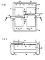
- connection pins are shown, although an integrated circuit usually has significantly more connection pins, as is known to the person skilled in the art.
- Figure 1 shows the known circuit in the open state in plan view.
- Figure 2 shows the circuit of Figure 1 in cross section along a section line II (see Figure 1), but in the non-opened state.
- a plastic mass M which can usually be produced by spraying the plastic mass M, serves as the housing.
- a semiconductor chip CH is hermetically enclosed within the housing, ie within the plastic mass M.
- the semiconductor chip CH has pads Pd (generally known as "pads") for contacting the semiconductor chip CH.
- the circuit also contains so-called leads L, which are also used to contact the semiconductor chip CH. They are arranged according to the so-called LOC technology, i.e. above the semiconductor chip CH. Depending on their function, the leads L have several sections (1, 2, 3, P): in a first section 1, a respective lead L is mechanically stably connected to a respective pad Pd (B), for example by means of a wire. Such a connection B is generally referred to as a bond connection.
- the leads L are guided in the second section 2 through the plastic mass M of the integrated circuit to the outside. Outside the integrated circuit, they form connections of the circuit, generally referred to as pins P.
- the third section 3 of a respective lead L is located within the housing of the integrated circuit. It also includes the first section 1 of the respective lead L. It connects to the second section 2.
- a double-sided adhesive film F is provided on that surface of the semiconductor chip CH which has the connection areas Pd, which is arranged between the surface of the semiconductor chip CH and the leads L. It covers practically the entire surface with the exception of those areas in which the pads Pd are arranged. If, as assumed in the integrated circuit according to FIGS. 1, 2, the semiconductor chip CH has connection pads Pd which are arranged along an assumed central axis of the semiconductor chip CH, instead of a single adhesive film F two adhesive films F are arranged next to one another such that the connection pads Pd remain free.
- the adhesive film F essentially serves two purposes: on the one hand, before and during the spraying process, ie before and during the application of the housing, it serves to securely fix the leads L with respect to the semiconductor chip CH, so that in particular no damage to the connections B can occur (for example by unintentionally moving the leads L). On the other hand, it protects the surface of the semiconductor chip CH against damage from the leads L, in particular against damage from scratches. In this circuit ( Figures 1, 2) according to the prior art, the disadvantages and damage described above occur.
- Figures 3 and 4 show a first embodiment of the integrated circuit according to the invention in plan view ( Figure 3) and in cross section ( Figure 4).
- the embodiment according to FIGS. 3, 4 has the same features as the circuit according to FIGS. 1, 2 with the exception of the adhesive film F.
- An adhesive film F according to FIGS. 1, 2, which essentially covers the entire semiconductor chip CH, is in the circuit according to the invention not provided. Instead, an adhesive Adh is applied to each individual lead L between the lead L and the semiconductor chip CH. It is located essentially exclusively between the respective lead L and the semiconductor chip CH, apart from a small amount of excess adhesive Adh that may swell laterally when the leads L are applied.
- Adb calf material so applied is the same as that regarding of the circuit according to Figures 1, 2 already described purpose of the adhesive film F, namely fixing of the leads L before and during the spraying process and protection against damage to the semiconductor chip CH by the leads L.
- those surface areas of the semiconductor chip CH are consequently , which are between the leads L, free of adhesive film F or adhesive Adh.
- adhesive Adh adhesive Adh
- Figures 5 and 6 show a second embodiment of the circuit according to the invention. It largely corresponds to the first embodiment described. However, as in the first embodiment, the adhesive Adh is not arranged in the entire area of the third section 3 of a respective lead L, but rather only in a partial area III of the third section 3. The partial area III in particular comprises the first section 1, as shown in FIG. 6 evident.
- Figures 7 and 8 show a third embodiment of the invention. It is a further development of the second embodiment and differs from it in that the partial area III is essentially point-shaped.
- the section III designed in this way is located below the location of the first section 1 at which the connection B is fastened on the lead L in question.
- FIG. 9 shows a section of one of the third embodiment derived fourth embodiment of the circuit according to the invention. It differs from the third embodiment in that the leads L are cranked at that point of the third section 3 at which the respective section III begins.
- This has the advantage that during the spraying process between the leads L and the surface of the semiconductor chip CH, more plastic mass M can accumulate in the subregions of the third sections 3 remaining outside the subregions III than in the previously described embodiments, because the distances between the leads L and the semiconductor chip CH are correspondingly larger at the relevant points. This leads to greater mechanical stabilization of the leads by the spraying process.
- the first sections 1 each lie in the partial areas III of the third sections 3.
- Figure 10 shows a further advantageous embodiment of the invention.
- At least one of the leads L of the circuit in the third section 3 has a plurality of first sections 1 and a plurality of sub-areas III.
- a respective first section 1 is located in a respective sub-area III.
- the circuit can then be supplied with a supply potential (VDD or VSS) at several locations on the semiconductor chip CH at the same time, with a lower voltage drop due to an ohmic resistance along the relevant leads L than with a supply via a connecting line within the circuit
- FIGS. 3 to 8 and 10 show a further advantageous feature in addition to the features described so far: in this case, on the surface of the semiconductor chip CH having the connection surfaces Pd, edge regions R which run along longitudinal sides R1 of the semiconductor chip CH are free of pads Pd. With this arrangement, it is possible to design electrical circuits, which are contained in the semiconductor chip CH, in terms of their layout such that they extend into these edge regions R. This leads to better utilization of the chip area of the semiconductor chip CH by the electrical circuits contained in the semiconductor chip CH.
Abstract
Description
Die Erfindung betrifft einen integrierten Schaltkreis nach dem Oberbegriff des Patentanspruches 1.The invention relates to an integrated circuit according to the preamble of claim 1.
Ein gattungsgemäßer Schaltkreis ist bekannt aus "IEEE Proceedings of the 38th ECC, Los Angeles 1988", Seiten 552 bis 557: "Volume Production of Unique Plastic Surface-Mount Modules for the IBM 80-ns 1-Mbit DRAM Chip by Area Wire Bond Techniques". Bei diesem Schaltkreis sind die zur Kontaktierung des Schaltkreises verwendeten Leads oberhalb des im Schaltkreis enthaltenen Halbleiterchips angeordnet. Eine solche Anordnung ist der Fachwelt bekannt unter dem Begriff "LOC-Technik" (= Lead on Chip). Um die Oberfläche des Halbleiterchips vor Verletzungen durch die Leads zu schützen (Verletzungen könnten z.B. bei der Montage von Halbleiterchip und Leads in einem Gehäuse auftreten) und um gleichzeitig die Leads bzgl. des Halbleiterchips zu fixieren, sind auf der Chipoberfläche Selbstklebefolien großflächig angeordnet.A generic circuit is known from "IEEE Proceedings of the 38th ECC, Los Angeles 1988", pages 552 to 557: "Volume Production of Unique Plastic Surface-Mount Modules for the IBM 80-ns 1-Mbit DRAM Chip by Area Wire Bond Techniques ". In this circuit, the leads used for contacting the circuit are arranged above the semiconductor chip contained in the circuit. Such an arrangement is known to the art, the term "LOC technique" (= L ead o n C hip). In order to protect the surface of the semiconductor chip from injuries caused by the leads (injuries could occur, for example, when mounting the semiconductor chip and leads in a housing) and at the same time to fix the leads with respect to the semiconductor chip, self-adhesive films are arranged on the chip surface over a large area.
Erprobungen solcher Schaltkreise haben gezeigt, daß insbesondere bei ständig wechselnden Temperaturverhältnissen Schäden auftreten wie z.B. Risse im Schaltkreisgehäuse und Brüche des Halbleiterchips. Als Ursache für diese Schäden konnte ermittelt werden, daß aufgrund der Temperaturänderungen zwischen der Plastikmasse des Gehäuses eines solchen Schaltkreises und den Selbstklebefolien Delamination auftritt. In geringerem Umfang tritt diese Delamination auch zwischen den Selbstklebefolien und dem Halbleiterchip auf. Während der Halbleiterchip an seiner Oberfläche bzw. die darauf befindlichen Selbstklebefolien aufgrund dieser Delamination lose sind gegenüber dem Schaltkreisgehäuse, ist der Halbleiterchip an seiner Unterseite fest mit dem Schaltkreisgehäuse verbunden. Aufgrund unterschiedlicher Wärmeausdehnungskoeffizienten von Gehäuse und Halbleiterchip bilden sich bei Temperaturänderungen an der Chipoberseite Scherkräfte aus, die letztendlich zu den beschriebenen Schäden führen.Tests of such circuits have shown that damage occurs in particular in the case of constantly changing temperature conditions, for example cracks in the circuit housing and breaks in the semiconductor chip. The cause of this damage was found to be delamination due to the temperature changes between the plastic mass of the housing of such a circuit and the self-adhesive films. This delamination also occurs to a lesser extent between the self-adhesive films and the semiconductor chip. While the semiconductor chip on its surface or the self-adhesive films thereon due to this Delamination are loose compared to the circuit housing, the semiconductor chip is firmly connected to the circuit housing on its underside. Due to different coefficients of thermal expansion of the housing and the semiconductor chip, shear forces develop when the temperature changes on the upper side of the chip, which ultimately leads to the damage described.
Aufgabe der vorliegenden Erfindung ist es, einen integrierten Schaltkreis zu schaffen, bei dem solche Schäden nicht auftreten können.The object of the present invention is to provide an integrated circuit in which such damage cannot occur.
Diese Aufgabe wird bei einem gattungsgemäßen Schaltkreis gelöst mittels der kennzeichnenden Merkmale des Patentanspruches 1. Vorteilhafte Aus- und Weiterbildungen sind in Unteransprüchen gekennzeichnet.This object is achieved in a generic circuit by means of the characterizing features of claim 1. Advantageous training and further developments are characterized in the subclaims.
Die Erfindung wird nachstehend anhand der Zeichnung erläutert. Es zeigen:
- Die Figuren 1 und 2
- den bekannten Schaltkreis in Draufsicht und im Querschnitt,
- die
Figuren 3 bis 8 und 10 - verschiedene Ausführungsformen des erfindungsgemäßen Schaltkreises, jeweils in Draufsicht und Querschnitt,
- die Figur 9
- eine vorteilhafte Einzelheit.
- Figures 1 and 2
- the known circuit in plan view and in cross section,
- Figures 3 to 8 and 10
- different embodiments of the circuit according to the invention, each in top view and cross section,
- the figure 9
- an advantageous detail.
Aus Gründen der Übersichtlichkeit sind die Darstellungen auf das Wesentliche beschränkt. Insbesondere sind lediglich zwei Anschlußpins dargestellt, obwohl ein integrierter Schaltkreis üblicherweise wesentlich mehr Anschlußpins aufweist, wie dem Fachmann bekannt ist.For reasons of clarity, the representations are limited to the essentials. In particular, only two connection pins are shown, although an integrated circuit usually has significantly more connection pins, as is known to the person skilled in the art.
Figur 1 zeigt den bekannten Schaltkreis in geöffnetem Zustand in Draufsicht. Figur 2 zeigt den Schaltkreis nach Figur 1 im Querschnitt entlang einer Schnittlinie II (siehe Figur 1), allerdings im nicht-geöffneten Zustand. Als Gehäuse dient eine Plastikmasse M, welches üblicherweise mittels Spritzens der Plastikmasse M herstellbar ist. Innerhalb des Gehäuses, d.h. innerhalb der Plastikmasse M, ist ein Halbleiterchip CH hermetisch eingeschlossen. Der Halbleiterchip CH weist Anschlußflächen Pd auf (allgemein als "pads" bekannt) zur Kontaktierung des Halbleiterchips CH.Figure 1 shows the known circuit in the open state in plan view. Figure 2 shows the circuit of Figure 1 in cross section along a section line II (see Figure 1), but in the non-opened state. A plastic mass M, which can usually be produced by spraying the plastic mass M, serves as the housing. A semiconductor chip CH is hermetically enclosed within the housing, ie within the plastic mass M. The semiconductor chip CH has pads Pd (generally known as "pads") for contacting the semiconductor chip CH.
Weiterhin enthält der Schaltkreis sogenannte Leads L, die ebenfalls der Kontaktierung des Halbleiterchips CH dienen. Sie sind entsprechend der sogenannten LOC-Technik angeordnet, d.h. oberhalb des Halbleiterchips CH. Die Leads L weisen, entsprechend ihrer Funktion, mehrere Abschnitte (1, 2, 3, P) auf: In einem ersten Abschnitt 1 ist ein jeweiliges Lead L mit einer jeweiligen Anschlußfläche Pd mechanisch stabil verbunden (B), beispielsweise mittels eines Drahtes. Eine solche Verbindung B wird im allgemeinen als Bond-Verbindung bezeichnet. Die Leads L sind im zweiten Abschnitt 2 durch die Plastikmasse M des integrierten Schaltkreises hindurch nach außen geführt. Außerhalb des integrierten Schaltkreises bilden sie allgemein als Pins P bezeichnete Anschlüsse des Schaltkreises. Der dritte Abschnitt 3 eines jeweiligen Leads L befindet sich innerhalb des Gehäuses des integrierten Schaltkreises. Er umfaßt auch den ersten Abschnitt 1 des jeweiligen Leads L. Er schließt sich an den zweiten Abschnitt 2 an.The circuit also contains so-called leads L, which are also used to contact the semiconductor chip CH. They are arranged according to the so-called LOC technology, i.e. above the semiconductor chip CH. Depending on their function, the leads L have several sections (1, 2, 3, P): in a first section 1, a respective lead L is mechanically stably connected to a respective pad Pd (B), for example by means of a wire. Such a connection B is generally referred to as a bond connection. The leads L are guided in the
Bei diesem integrierten Schaltkreis nach dem Stande der Technik ist auf derjenigen Oberfläche des Halbleiterchips CH, welche die Anschlußflächen Pd aufweist, eine doppelseitige Klebefolie F vorgesehen, die zwischen der Oberfläche des Halbleiterchips CH und den Leads L angeordnet ist. Sie umfaßt praktisch die gesamte Oberfläche mit Ausnahme derjenigen Bereiche, in denen die Anschlußflächen Pd angeordnet sind. Falls, wie beim integrierten Schaltkreis nach den Figuren 1, 2 angenommen, der Halbleiterchip CH Anschlußflächen Pd aufweist, die entlang einer angenommenen Mittelachse des Halbleiterchips CH angeordnet sind, so sind anstelle einer einzigen Klebefolie F zwei Klebefolien F nebeneinander so angeordnet, daß die Anschlußflächen Pd frei bleiben. Die Klebefolie F dient im wesentlichen zwei Zwecken: Zum einen dient sie vor und während des Spritzvorganges, d.h. vor und während des Aufbringens des Gehäuses, einem sicheren Fixieren der Leads L bezüglich des Halbleiterchips CH, so daß insbesondere keine Beschädigung der Verbindungen B auftreten können (beispielsweise durch unbeabsichtigtes Verschieben der Leads L). Zum anderen schützt sie die Oberfläche des Halbleiterchips CH vor Beschädigungen durch die Leads L, insbesondere vor Beschädigungen durch Kratzer. Bei diesem Schaltkreis (Figuren 1, 2) nach dem Stande der Technik treten die eingangs beschriebenen Nachteile und Schäden auf.In this integrated circuit according to the prior art, a double-sided adhesive film F is provided on that surface of the semiconductor chip CH which has the connection areas Pd, which is arranged between the surface of the semiconductor chip CH and the leads L. It covers practically the entire surface with the exception of those areas in which the pads Pd are arranged. If, as assumed in the integrated circuit according to FIGS. 1, 2, the semiconductor chip CH has connection pads Pd which are arranged along an assumed central axis of the semiconductor chip CH, instead of a single adhesive film F two adhesive films F are arranged next to one another such that the connection pads Pd remain free. The adhesive film F essentially serves two purposes: on the one hand, before and during the spraying process, ie before and during the application of the housing, it serves to securely fix the leads L with respect to the semiconductor chip CH, so that in particular no damage to the connections B can occur ( for example by unintentionally moving the leads L). On the other hand, it protects the surface of the semiconductor chip CH against damage from the leads L, in particular against damage from scratches. In this circuit (Figures 1, 2) according to the prior art, the disadvantages and damage described above occur.
Die Figuren 3 und 4 zeigen eine erste Ausführungsform des erfindungsgemäßen integrierten Schaltkreises in Draufsicht (Figur 3) und im Querschnitt (Figur 4). Die Ausführungsform nach den Figuren 3, 4 weist dieselben Merkmale auf wie der Schaltkreis nach den Figuren 1, 2 mit Ausnahme der Klebefolie F. Eine Klebefolie F entsprechend den Figuren 1, 2, die im wesentlichen den gesamten Halbleiterchip CH bedeckt, ist beim erfindungsgemäßen Schaltkreis nicht vorgesehen. Stattdessen ist bei jedem einzelnen Lead L zwischen dem Lead L und dem Halbleiterchip CH ein Klebstoff Adh aufgebracht. Er befindet sich im wesentlichen ausschließlich zwischen dem jeweiligen Lead L und dem Halbleiterchip CH, abgesehen von einer beim Aufbringen der Leads L ggf. seitlich hervorquellenden geringen Menge von Überschuß des Klebstoffes Adh. Sinn und Zweck des so aufgebrachten Kelbstoffes Adh ist derselbe wie der bezüglich des Schaltkreises nach den Figuren 1, 2 bereits beschriebene Sinn und Zweck der Klebefolie F, nämlich Fixieren der Leads L vor und während des Spritzvorganges sowie Schutz vor Beschädigung des Halbleiterchips CH durch die Leads L. Bei dem erfindungsgemäßen Schaltkreis sind demzufolge diejenigen Oberflächenbereiche des Halbleiterchips CH, die sich zwischen den Leads L befinden, frei von Klebefolie F bzw. Klebstoff Adh. Somit herrschen in diesen Oberflächenbereichen dieselben Adhäsionsverhältnisse bezüglich der diese Bereiche bedeckenden Teile der Plastikmasse M wie an der den Anschlußflächen Pd abgewandten Chipunterseite mit ihrer Oberfläche. Demzufolge können sich die bezüglich des Standes der Technik beschriebenen zerstörerischen Vorgänge und Kräfte nicht mehr aufbauen.Figures 3 and 4 show a first embodiment of the integrated circuit according to the invention in plan view (Figure 3) and in cross section (Figure 4). The embodiment according to FIGS. 3, 4 has the same features as the circuit according to FIGS. 1, 2 with the exception of the adhesive film F. An adhesive film F according to FIGS. 1, 2, which essentially covers the entire semiconductor chip CH, is in the circuit according to the invention not provided. Instead, an adhesive Adh is applied to each individual lead L between the lead L and the semiconductor chip CH. It is located essentially exclusively between the respective lead L and the semiconductor chip CH, apart from a small amount of excess adhesive Adh that may swell laterally when the leads L are applied. The meaning and purpose of the Adb calf material so applied is the same as that regarding of the circuit according to Figures 1, 2 already described purpose of the adhesive film F, namely fixing of the leads L before and during the spraying process and protection against damage to the semiconductor chip CH by the leads L. In the circuit according to the invention, those surface areas of the semiconductor chip CH are consequently , which are between the leads L, free of adhesive film F or adhesive Adh. Thus, in these surface areas there are the same adhesion conditions with respect to the parts of the plastic mass M covering these areas as with the surface of the chip underside facing away from the connection surfaces Pd. As a result, the destructive processes and forces described in relation to the prior art can no longer build up.
Die Figuren 5 und 6 zeigen eine zweite Ausführungsform des erfindungsgemäßen Schaltkreises. Sie entspricht großen Teils der beschriebenen ersten Ausführungsform. Allerdings ist der Klebstoff Adh nicht, wie der ersten Ausführungsform, im gesamten Bereich des dritten Abschnittes 3 eines jeweiligen Leads L angeordnet, sondern lediglich in einem Teilbereich III des dritten Abschnittes 3. Der Teilbereich III umfaßt insbesondere den ersten Abschnitt 1, wie aus Figur 6 ersichtlich.Figures 5 and 6 show a second embodiment of the circuit according to the invention. It largely corresponds to the first embodiment described. However, as in the first embodiment, the adhesive Adh is not arranged in the entire area of the
Die Figuren 7 und 8 zeigen eine dritte Ausführungsform der Erfindung. Sie ist eine Weiterbildung der zweiten Ausführungsform und unterscheidet sich von dieser dadurch, daß der Teilbereich III im wesentlichen punktförmig ausgestaltet ist. Vorteilhafterweise befindet sich der so ausgestaltete Teilbereich III unterhalb der Stelle des ersten Abschnittes 1, an der die Verbindung B auf dem betreffenden Lead L befestigt ist.Figures 7 and 8 show a third embodiment of the invention. It is a further development of the second embodiment and differs from it in that the partial area III is essentially point-shaped. Advantageously, the section III designed in this way is located below the location of the first section 1 at which the connection B is fastened on the lead L in question.
Figur 9 zeigt ausschnittsweise eine von der dritten Ausführungsform abgeleitete vierte Ausführungsform des erfindungsgemäßen Schaltkreises. Sie unterscheidet sich von der dritten Ausführungsform dadurch, daß die Leads L an derjenigen Stelle des dritten Abschnittes 3, an der der jeweilige Teilbereich III beginnt, gekröpft sind. Dies hat den Vorteil, daß sich beim Spritzvorgang zwischen den Leads L und der Oberfläche des Halbleiterchips CH in den außerhalb der Teilbereiche III verbleibenden Teilbereichen der dritten Abschnitte 3 mehr Plastikmasse M anlagern kann als bei den bisher beschriebenen Ausführungsformen, weil die Abstände zwischen den Leads L und dem Halbleiterchip CH an den betreffenden Stellen entsprechend größer sind. Dies hat eine größere mechanische Stabilisierung der Leads durch den Spritzvorgang zur Folge.FIG. 9 shows a section of one of the third embodiment derived fourth embodiment of the circuit according to the invention. It differs from the third embodiment in that the leads L are cranked at that point of the
Bei den Ausführungsformen nach den Figuren 5 bis 9 liegen, ebenso wie bei der noch zu beschreibenden Ausführungsform nach Figur 10, die ersten Abschnitte 1 jeweils in den Teilbereichen III der dritten Abschnitte 3.In the embodiments according to FIGS. 5 to 9, just as in the embodiment to be described according to FIG. 10, the first sections 1 each lie in the partial areas III of the
Figur 10 zeigt eine weitere vorteilhafte Ausführungsform der Erfindung. Dabei weist wenigstens eines der Leads L des Schaltkreises im dritten Abschnitt 3 mehrere erste Abschnitte 1 und mehrere Teilbereiche III auf. Dabei befindet sich ein jeweiliger erster Abschnitt 1 in einem jeweiligen Teilbereich III. Bei einer solchen Ausgestaltung läßt sich dem Schaltkreis im Betrieb dann beispielsweise ein Versorgungspotential (VDD oder VSS) an mehreren Stellen des Halbleiterchips CH gleichzeitig zuführen mit einem geringeren Spannungsabfall aufgrund eines ohm'schen Widerstandes entlang der betreffenden Leads L als bei einer Zuführung mittels Verbindungsleitung innerhalb des Halbleiterchips von einem einzigen ersten Abschnitt 1 aus, da eine solche Verbindungsleitung einen höheren ohm'schen Widerstand aufwiese als die Zuführung mittels mehrerer erster Abschnitte 1 (ein Lead L hat einen wesentlich größeren Querschnitt als eine Verbindungsleitung im Halbleiterchip CH).Figure 10 shows a further advantageous embodiment of the invention. At least one of the leads L of the circuit in the
Die Ausführungsformen nach den Figuren 3 bis 8 und 10 zeigen über die bislang beschriebenen Merkmale hinaus noch ein weiteres, vorteilhaftes Merkmal: Dabei sind auf der die Anschlußflächen Pd aufweisenden Oberfläche des Halbleiterchips CH Randbereiche R, die entlang von Längsseiten R1 des Halbleiterchips CH verlaufen, frei von Anschlußflächen Pd. Mit dieser Anordnung ist es möglich, elektrische Schaltungen, die im Halbleiterchip CH enthalten sind, bezüglich ihres Layouts so zu gestalten, daß sie bis in diese Randbereiche R reichen. Dies führt zu einem besseren Ausnützen der Chipfläche des Halbleiterchips CH durch die im Halbleiterchip CH enthaltenen elektrischen Schaltungen.The embodiments according to FIGS. 3 to 8 and 10 show a further advantageous feature in addition to the features described so far: in this case, on the surface of the semiconductor chip CH having the connection surfaces Pd, edge regions R which run along longitudinal sides R1 of the semiconductor chip CH are free of pads Pd. With this arrangement, it is possible to design electrical circuits, which are contained in the semiconductor chip CH, in terms of their layout such that they extend into these edge regions R. This leads to better utilization of the chip area of the semiconductor chip CH by the electrical circuits contained in the semiconductor chip CH.
Claims (9)
folgende Merkmale:
Zur Klebung ist je einzelnem Lead (L) zwischen dem Lead (L) und dem Halbleiterchip (CH) Klebstoff (Adh) angebracht, der sich im wesentlichen ausschließlich zwischen dem jeweiligen Lead (L) und dem Halbleiterchip (CH) befindet, so daß Oberflächenbereiche des Halbleiterchips (CH), die sich zwischen benachbarten Leads (L) befinden, frei vom Klebstoff (Adh) sind.Integrated circuit with the following features:
following features:
For bonding, each individual lead (L) is attached between the lead (L) and the semiconductor chip (CH) adhesive (Adh), which is essentially exclusively between the respective lead (L) and the semiconductor chip (CH), so that surface areas of the semiconductor chip (CH), which are located between adjacent leads (L), are free of adhesive (Adh).
dadurch gekennzeichnet,
daß der Klebstoff (Adh) bei einem jeweiligen Lead (L) im Bereich des gesamten dritten Abschnitts (3) zwischen dem Lead (L) und dem Halbleiterchip (CH) angeordnet ist.Integrated circuit according to Claim 1,
characterized,
that the adhesive (Adh) is arranged for a respective lead (L) in the region of the entire third section (3) between the lead (L) and the semiconductor chip (CH).
dadurch gekennzeichnet,
daß der Klebstoff (Adh) bei einem jeweiligen Lead (L) nur in einem Teilbereich (III) des dritten Abschnittes (3) zwischen dem Lead (L) und dem Halbleiterchip (CH) angeordnet ist.Integrated circuit according to Claim 1,
characterized,
that the adhesive (Adh) for each lead (L) only is arranged in a partial area (III) of the third section (3) between the lead (L) and the semiconductor chip (CH).
dadurch gekennzeichnet,
daß der Teilbereich (III) punktförmig ist.Integrated circuit according to Claim 3,
characterized,
that section (III) is punctiform.
dadurch gekennzeichnet,
daß das jeweilige Lead (L) im dritten Abschnitt (3) an derjenigen Stelle, wo der Teilbereich (III) beginnt, gekröpft ist.Integrated circuit according to Claim 3 or 4,
characterized,
that the respective lead (L) in the third section (3) is cranked at the point where the partial area (III) begins.
daß sich die ersten Abschnitte (1) in den Teilbereichen (III) der dritten Abschnitte (3) befinden.Integrated circuit according to one of Claims 3 to 5, characterized in that
that the first sections (1) are in the partial areas (III) of the third sections (3).
daß wenigstens eines der Leads (L) des Schaltkreises mehr als einen ersten Abschnitt (1) und mehr als einen Teilbereich (III) aufweist.Integrated circuit according to one of Claims 3 to 6, characterized in that
that at least one of the leads (L) of the circuit has more than a first section (1) and more than one section (III).
dadurch gekennzeichnet,
daß sich ein jeweiliger erster Abschnitt (1) in einem jeweiligen Teilbereich (III) des dritten Abschnitts (3) befindet.Integrated circuit according to Claim 7,
characterized,
that a respective first section (1) is located in a respective partial area (III) of the third section (3).
daß Randbereiche (R) des Halbleiterchips (CH), die entlang von Längsseiten (R1) des Halbleiterchips (CH) verlaufen, frei von Kontaktflächen (Pd) sind.Integrated circuit according to one of the preceding claims, characterized in that
that edge regions (R) of the semiconductor chip (CH), which run along longitudinal sides (R1) of the semiconductor chip (CH), are free of contact surfaces (Pd).
Priority Applications (2)
| Application Number | Priority Date | Filing Date | Title |
|---|---|---|---|
| EP92111167A EP0576708A1 (en) | 1992-07-01 | 1992-07-01 | Integrated circuit with leadframe |
| JP5173812A JPH0685150A (en) | 1992-07-01 | 1993-06-21 | Integrated circuit |
Applications Claiming Priority (1)
| Application Number | Priority Date | Filing Date | Title |
|---|---|---|---|
| EP92111167A EP0576708A1 (en) | 1992-07-01 | 1992-07-01 | Integrated circuit with leadframe |
Publications (1)
| Publication Number | Publication Date |
|---|---|
| EP0576708A1 true EP0576708A1 (en) | 1994-01-05 |
Family
ID=8209767
Family Applications (1)
| Application Number | Title | Priority Date | Filing Date |
|---|---|---|---|
| EP92111167A Withdrawn EP0576708A1 (en) | 1992-07-01 | 1992-07-01 | Integrated circuit with leadframe |
Country Status (2)
| Country | Link |
|---|---|
| EP (1) | EP0576708A1 (en) |
| JP (1) | JPH0685150A (en) |
Cited By (4)
| Publication number | Priority date | Publication date | Assignee | Title |
|---|---|---|---|---|
| DE4435115A1 (en) * | 1994-09-30 | 1996-04-04 | Siemens Ag | Lead on chip system using multi-layer tape |
| US5684330A (en) * | 1995-08-22 | 1997-11-04 | Samsung Electronics Co., Ltd. | Chip-sized package having metal circuit substrate |
| DE19633712C1 (en) * | 1996-08-21 | 1998-04-16 | Siemens Components | Adhesive band application device for lead-frame |
| US5917242A (en) * | 1996-05-20 | 1999-06-29 | Micron Technology, Inc. | Combination of semiconductor interconnect |
Families Citing this family (1)
| Publication number | Priority date | Publication date | Assignee | Title |
|---|---|---|---|---|
| JP3638750B2 (en) * | 1997-03-25 | 2005-04-13 | 株式会社ルネサステクノロジ | Semiconductor device |
Citations (4)
| Publication number | Priority date | Publication date | Assignee | Title |
|---|---|---|---|---|
| EP0329317A2 (en) * | 1988-02-12 | 1989-08-23 | Hitachi, Ltd. | Semiconductor device having an insulating sheet |
| EP0409173A2 (en) * | 1989-07-19 | 1991-01-23 | Nec Corporation | Semiconductor ic device having an improved interconnection structure |
| US5086018A (en) * | 1991-05-02 | 1992-02-04 | International Business Machines Corporation | Method of making a planarized thin film covered wire bonded semiconductor package |
| EP0478250A1 (en) * | 1990-09-24 | 1992-04-01 | Texas Instruments Incorporated | Integrated circuit device and method to prevent cracking during surface mount |
Family Cites Families (4)
| Publication number | Priority date | Publication date | Assignee | Title |
|---|---|---|---|---|
| JPH0327562A (en) * | 1989-06-23 | 1991-02-05 | Nec Corp | Semiconductor device |
| JP2569939B2 (en) * | 1989-10-23 | 1997-01-08 | 日本電気株式会社 | Resin-sealed semiconductor device |
| JPH03235360A (en) * | 1990-02-09 | 1991-10-21 | Nec Corp | Plastic molded type semiconductor device |
| JP2983620B2 (en) * | 1990-07-20 | 1999-11-29 | 株式会社日立製作所 | Semiconductor device and manufacturing method thereof |
-
1992
- 1992-07-01 EP EP92111167A patent/EP0576708A1/en not_active Withdrawn
-
1993
- 1993-06-21 JP JP5173812A patent/JPH0685150A/en active Pending
Patent Citations (4)
| Publication number | Priority date | Publication date | Assignee | Title |
|---|---|---|---|---|
| EP0329317A2 (en) * | 1988-02-12 | 1989-08-23 | Hitachi, Ltd. | Semiconductor device having an insulating sheet |
| EP0409173A2 (en) * | 1989-07-19 | 1991-01-23 | Nec Corporation | Semiconductor ic device having an improved interconnection structure |
| EP0478250A1 (en) * | 1990-09-24 | 1992-04-01 | Texas Instruments Incorporated | Integrated circuit device and method to prevent cracking during surface mount |
| US5086018A (en) * | 1991-05-02 | 1992-02-04 | International Business Machines Corporation | Method of making a planarized thin film covered wire bonded semiconductor package |
Cited By (6)
| Publication number | Priority date | Publication date | Assignee | Title |
|---|---|---|---|---|
| DE4435115A1 (en) * | 1994-09-30 | 1996-04-04 | Siemens Ag | Lead on chip system using multi-layer tape |
| DE4435115C2 (en) * | 1994-09-30 | 1999-01-21 | Siemens Ag | Method of manufacturing a lead-on-chip (LOC) device |
| US5684330A (en) * | 1995-08-22 | 1997-11-04 | Samsung Electronics Co., Ltd. | Chip-sized package having metal circuit substrate |
| US5917242A (en) * | 1996-05-20 | 1999-06-29 | Micron Technology, Inc. | Combination of semiconductor interconnect |
| US6080264A (en) * | 1996-05-20 | 2000-06-27 | Micron Technology, Inc. | Combination of semiconductor interconnect |
| DE19633712C1 (en) * | 1996-08-21 | 1998-04-16 | Siemens Components | Adhesive band application device for lead-frame |
Also Published As
| Publication number | Publication date |
|---|---|
| JPH0685150A (en) | 1994-03-25 |
Similar Documents
| Publication | Publication Date | Title |
|---|---|---|
| EP0299530B1 (en) | Support for inclusion into identity cards | |
| EP0484353B1 (en) | Substrate element with at least one integrated circuit, in particular a substrate element for inclusion in chip cards | |
| EP0682321B1 (en) | Record carrier with integrated circuit and procedure for manufacturing a record carrier | |
| DE69938582T2 (en) | SEMICONDUCTOR ELEMENT, ITS MANUFACTURE, PCB AND ELECTRONIC APPARATUS | |
| DE69839276T2 (en) | METHOD FOR PRODUCING A CHIP CARD, SUITABLE FOR CONTACTED OR CONTACTLESS OPERATION | |
| DE3814469C2 (en) | ||
| DE2732529C2 (en) | Printed circuit board | |
| DE3616494A1 (en) | INTEGRATED CIRCUIT BOX AND METHOD FOR PRODUCING AN INTEGRATED CIRCUIT BOX | |
| DE10352946A1 (en) | Semiconductor component with semiconductor chip and rewiring layer and method for producing the same | |
| DE19755675B4 (en) | Semiconductor package and method for its manufacture | |
| DE102006033864A1 (en) | Electronic circuit in a package-in-package configuration and method of manufacturing such a circuit | |
| EP0951692A1 (en) | Carrier element for a semiconductor chip for installing in chip cards | |
| EP0009610A1 (en) | Method for producing testable semiconductor miniature containers in strip form | |
| EP0576708A1 (en) | Integrated circuit with leadframe | |
| DE10255289A1 (en) | Electronic component with stacked semiconductor chips in a parallel arrangement and method for its production | |
| DE3130072A1 (en) | INTEGRATED SWITCHING LINK | |
| EP1065624A2 (en) | Chip module for installation in a chip card carrier | |
| DE19743264C2 (en) | Method for producing an emulation circuit arrangement and emulation circuit arrangement with two integrated circuits | |
| DE4130569A1 (en) | IC PACKING DEVICE | |
| DE2528119A1 (en) | ELECTRIC CONDUCTIVE TAPE | |
| DE3619636A1 (en) | Housing for integrated circuits | |
| EP0852774B1 (en) | Chip module | |
| DE4113034A1 (en) | SYSTEM AND METHOD FOR AUTOMATED TAPE BONDING, WHICH EASIER TO REPAIR | |
| WO1998033211A1 (en) | Method for casing integrated circuits | |
| DE4425943B4 (en) | Method for producing a multilayer conductor element or connecting element and conductor or connection element |
Legal Events
| Date | Code | Title | Description |
|---|---|---|---|
| PUAI | Public reference made under article 153(3) epc to a published international application that has entered the european phase |
Free format text: ORIGINAL CODE: 0009012 |
|
| AK | Designated contracting states |
Kind code of ref document: A1 Designated state(s): AT DE FR GB IT NL |
|
| 17P | Request for examination filed |
Effective date: 19940620 |
|
| 17Q | First examination report despatched |
Effective date: 19960325 |
|
| STAA | Information on the status of an ep patent application or granted ep patent |
Free format text: STATUS: THE APPLICATION IS DEEMED TO BE WITHDRAWN |
|
| 18D | Application deemed to be withdrawn |
Effective date: 19960806 |