EP0573183B2 - Probe station with integrated environment control enclosure - Google Patents
Probe station with integrated environment control enclosure Download PDFInfo
- Publication number
- EP0573183B2 EP0573183B2 EP93303937A EP93303937A EP0573183B2 EP 0573183 B2 EP0573183 B2 EP 0573183B2 EP 93303937 A EP93303937 A EP 93303937A EP 93303937 A EP93303937 A EP 93303937A EP 0573183 B2 EP0573183 B2 EP 0573183B2
- Authority
- EP
- European Patent Office
- Prior art keywords
- enclosure
- probe station
- probe
- holder
- positioning mechanism
- Prior art date
- Legal status (The legal status is an assumption and is not a legal conclusion. Google has not performed a legal analysis and makes no representation as to the accuracy of the status listed.)
- Expired - Lifetime
Links
Images


Classifications
-
- H—ELECTRICITY
- H01—ELECTRIC ELEMENTS
- H01L—SEMICONDUCTOR DEVICES NOT COVERED BY CLASS H10
- H01L21/00—Processes or apparatus adapted for the manufacture or treatment of semiconductor or solid state devices or of parts thereof
- H01L21/67—Apparatus specially adapted for handling semiconductor or electric solid state devices during manufacture or treatment thereof; Apparatus specially adapted for handling wafers during manufacture or treatment of semiconductor or electric solid state devices or components ; Apparatus not specifically provided for elsewhere
- H01L21/68—Apparatus specially adapted for handling semiconductor or electric solid state devices during manufacture or treatment thereof; Apparatus specially adapted for handling wafers during manufacture or treatment of semiconductor or electric solid state devices or components ; Apparatus not specifically provided for elsewhere for positioning, orientation or alignment
Definitions
- the present invention is directed to probe stations for making highly accurate measurements of highspeed, large scale integrated circuits at the wafer level, and of other electronic devices. More particularly, the invention relates to such a probe station having a controlled-environment enclosure for isolating the wafer-supporting chuck and probe(s) from outside influences such as electromagnetic interference (EMI), moist air during low-temperature measurements, and/or light.
- EMI electromagnetic interference
- an enclosure For sensitive probing applications where electromagnetic interference or light must be eliminated, or where probing must be conducted at low test temperatures, an enclosure must be provided surrounding the test area. For low-temperature testing, the enclosure must provide a substantially hermetic seal for the introduction of a dry purge gas, such as nitrogen or dry air, to prevent condensation of moisture onto the waler at the low test temperature.
- a dry purge gas such as nitrogen or dry air
- a probe station with an enclosure and stationary probes is disclosed in US-A-3 710 251.
- US-A-3 333 274 a further probe station is disclosed.
- DE-A-3114 466 seals which allow lateral movement are disclosed.
- a probe station comprising a substantially planar surface for holding a test device on said surface, a holder for an electric probe for contacting the test device, and a pair of positioning mechanisms for selectively moving both said surface and said holder, independently of each other, toward or away from the other, one of said positioning mechanisms providing X-Y movement of said surface a compact enclosure surrounding said surface and providing a controlled environment, the integrity of which can be maintained despite movement by said positioning mechanisms of each one of said surface and holder, respectively, toward or away from the other along an axis of approach, in the Z-direction and despite said X-Y movement of said surface which movement is within the enclosure each one of said pair of positioning mechanisms being located at least partially outside of said enclosure, and extending between the exterior and interior of the enclosure said enclosure including an upper section having a plate extending laterally above said surface and a side wall fixed to said plate and surrounding said surface laterally.
- the present invention compatibly solves all of the foregoing drawbacks of the prior probe stations by providing a probe station according to claim 1.
- the integrity of its EMI, hermetic, and/or light sealing capability is maintained throughout movement by the positioning mechanism of the wafer supporting surface or probe holder along the axis of approach, or along the other positioning axes.
- Such maintenance of the sealing integrity of the enclosure despite positioning movement is made possible by extending the positioning mechanism or mechanisms movably and sealably between the exterior and interior of the enclosure.
- the sealing provided by the enclosure in the preferred embodiment is effective with respect to all three major environmental influences, i.e. EMI, substantial air leakage, and light; however it is within the scope of the invention for the sealing capability to be effective with respect to any one or more of these influences, depending upon the application for which the probe station is intended.
- multiple positioning mechanisms extend between the exterior and interior of the enclosure for positioning the wafer-supporting surface, the probes independently, and the probes in unison; however it is within the scope of the invention to provide any one or more of such positioning mechanisms in conjunction with the enclosure.
- an exemplary embodiment of the probe station of the present invention comprises a base 10 (shown partially) which supports a platen 12 through a number of jacks 14a, 14b, 14c, 14d which selectively raise and lower the platen vertically relative to the base by a small increment (approximately one-tenth of an inch) for purposes to be described hereafter. Also supported by the base 10 of the probe station is a motorized wafer positioner 16 having a rectangular plunger 18 which supports a movable chuck assembly 20.
- the chuck assembly 20 passes freely through a large aperture 22 in the platen 12 which permits the chuck assembly to be moved independently of the platen by the positioner 16 along X, Y and Z axes, i.e. horizontally along two mutually-perpendicular axes X and Y, and vertically along the Z axis.
- the platen 12 when moved vertically by the jacks 14, moves independently of the chuck assembly 20 and the positioner 16.
- the wafer probe 30 has a downwardly-inclined coplanar transmission line probe tip 32 for contacting wafers and other test devices mounted atop the chuck assembly 20, although other kinds of tips can be used as well.
- the probe positioner 24 has micrometer adjustments 34, 36 and 38 for adjusting the position of the probe holder 28, and thus the probe 30, along the X, Y and Z axes respectively, relative to the chuck assembly 20.
- the Z axis is exemplary of what is referred to herein loosely as the "axis of approach" between the probe holder 28 and the chuck assembly 20, although directions of approach which are neither vertical nor linear, along which the probe tip and wafer or other test device are brought into contact with each other, are also intended to be included within the meaning of the term "axis of approach.”
- a further micrometer adjustment 40 adjustably tilts the probe holder 28 so that the plane of the probe tip 32 can be made parallel to the plane of the wafer or other test device supported by the chuck assembly 20.
- As many as twelve individual probe positioners 24, each supporting a respective probe may be arranged on the platen 12 around the chuck assembly 20 so as to converge radially toward the chuck assembly similarly to the spokes of a wheel.
- each individual positioner 24 can independently adjust its respective probe in the X, Y and Z directions, while the jacks 14 can be actuated to raise or lower the platen 12 and thus all of the positioners 24 and their respective probes in unison.
- An environment control enclosure is composed of an upper box portion 42 rigidly attached to the platen 12, and a lower box portion 44 rigidly attached to the base 10. Both portions are made of steel or other suitable electrically conductive material to provide EMI shielding.
- an electrically conductive resilient foam gasket 46 preferably composed of silver or carbon-impregnated silicone, is interposed peripherally at their mating juncture at the front of the enclosure and between the lower portion 44 and the platen 12 so that an EMI, substantially hermetic, and light seal are all maintained despite relative vertical movement between the two box portions 42 and 44.
- a similar gasket 47 is preferably interposed between the portion 42 and the top of the platen to maximize sealing.
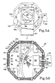
- the top of the upper box portion 42 comprises an octagonal steel box 48 having eight side panels such as 49a and 49b through which the extending members 26 of the respective probe positioners 24 can penetrate movably.
- Each panel comprises a hollow housing in which a respective sheet 50 of resilient foam, which may be similar to the above-identified gasket material, is placed. Slits such as 52 are partially cut vertically in the foam in alignment with slots 54 formed in the inner and outer surfaces of each panel housing, through which a respective extending member 26 of a respective probe positioner 24 can pass movably.
- the slitted foam permits X, Y and Z movement of the extending members 26 of each probe positioner, while maintaining the EMI, substantially hermetic, and light seal provided by the enclosure.
- the foam sheet 50 is sandwiched between a pair of steel plates 55 having slots 54 therein, such plates being slidable transversely within the panel housing through a range of movement encompassed by larger slots 56 in the inner and outer surfaces of the panel housing.
- a circular viewing aperture 58 is provided, having a recessed circular transparent sealing window 60 therein.
- a bracket 62 holds an apertured sliding shutter 64 to selectively permit or prevent the passage of light through the window.
- a stereoscope (not shown) connected to a CRT monitor can be placed above the window to provide a magnified display of the wafer or other test device and the probe tip for proper probe placement during set-up or operation.
- the window 60 can be removed and a microscope lens (not shown) surrounded by a foam gasket can be inserted through the viewing aperture 58 with the foam providing EMI, hermetic and light sealing.
- the upper box portion 42 of the environment control enclosure also includes a hinged steel door 68 which pivots outwardly about the pivot axis of a hinge 70 as shown in FIG. 2A.
- the hinge biases the door downwardly toward the top of the upper box portion 42 so that it forms a tight, overlapping, sliding peripheral seal 68a with the top of the upper box portion.
- the sealing integrity of the enclosure is likewise maintained throughout positioning movements by the motorized positioner 16 due to the provision of a series of four sealing plates 72, 74, 76 and 78 stacked slidably atop one another.
- the sizes of the plates progress increasingly from the top to the bottom one, as do the respective sizes of the central apertures 72a, 74a, 76a and 78a formed in the respective plates 72, 74, 76 and 78, and the aperture 79a formed in the bottom 44a of the lower box portion 44.
- the central aperture 72a in the top plate 72 mates closely around the bearing housing 18a of the vertically-movable plunger 18.
- the next plate in the downward progression, plate 74 has an upwardly-projecting peripheral margin 74b which limits the extent to which the plate 72 can slide across the top of the plate 74.
- the central aperture 74a in the plate 74 is of a size to permit the positioner 16 to move the plunger 18 and its bearing housing 18a transversely along the X and Y axes until the edge of the top plate 72 abuts against the margin 74b of the plate 74.
- the size of the aperture 74a is, however, too small to be uncovered by the top plate 72 when such abutment occurs, and therefore a seal is maintained between the plates 72 and 74 regardless of the movement of the plunger 18 and its bearing housing along the X and Y axes.
- This combination of sliding plates and central apertures of progressively increasing size permits a full range of movement of the plunger 18 along the X and Y axes by the positioner 16, while maintaining the enclosure in a sealed condition despite such positioning movement.
- the EMI sealing provided by this structure is effective even with respect to the electric motors of the positioner 16, since they are located below the sliding plates.
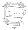
- the chuck assembly 20 is of a unique modular construction usable either with or without an environment control enclosure.
- the plunger 18 supports an adjustment plate 81 which in turn supports a rectangular stage 83 which detachably mounts a circular wafer chuck 80 of conventional design by means of screws such as 87. Shims such as 85 providing leveling.
- the wafer chuck 80 has a planar upwardly-facing wafer-supporting surface 82 having an array of vertical apertures 84 therein. These apertures communicate with respective chambers separated by O-rings 88, the chambers in turn being connected separately to different vacuum lines 90a, 90b, 90c communicating through separately-controlled vacuum valves (not shown) with a source of vacuum.
- the respective vacuum lines selectively connect the respective chambers and their apertures to the source of vacuum to hold the wafer, or alternatively isolate the apertures from the source of vacuum to release the wafer, in a conventional manner.
- the separate operability of the respective chambers and their corresponding apertures enables the chuck to hold wafers of different diameters.
- auxiliary chucks such as 92 and 94 are detachably mounted on the corners of the stage 83 by screws such as 96 independently of the wafer chuck 80.
- Each auxiliary chuck 92, 94 has its own separate upwardly-facing planar surface 100, 102 respectively, in parallel relationship to the surface 82 of the wafer chuck 80.
- Vacuum apertures 104 protrude through the surfaces 100 and 102 from communication with respective chambers 106, 108 within the body of each auxiliary chuck.
- Each of these chambers in turn communicates through a separate vacuum line 110 and a separate independently-actuated vacuum valve 114 with a source of vacuum 118 as shown schematically in FIG. 3.
- Each of the valves 114 selectively connects or isolates a respective chamber 106 or 108 with respect to the source of vacuum independently of the operation of the apertures 84 of the wafer chuck 80, so as to selectively hold or release a contact substrate or calibration substrate located on the respective surfaces 100 and 102 of the auxiliary chucks independently of the wafer.
- auxiliary chuck shims such as 120 can be inserted between the stage 83 and the auxiliary chuck to adjust the elevation of the auxiliary chuck's upper surface relative to that of the wafer chuck 80 and the otherauxiliary chuck(s). This compensates for any differences in' thicknesses between the wafer, contact substrate and calibration substrate which are simultaneously carried by the chuck assembly 20, so that the probes are easily transferable from one to the other without differences in contact pressure or the threat of damage to the probe tips.
- the vacuum valves 114 of the respective auxiliary chucks are located remotely from the chucks, and preferably exterior of the enclosure as indicated schematically in FIG. 3 to enable control of the auxiliary chucks despite the impediment to access created by the enclosure.
- This enables use of auxiliary chucks compatibly with such an enclosure, which is particularly critical because the presence of the auxiliary chucks eliminates the need for repetitive unloading and loading of contact substrates and calibration substrates during set-up and calibration, and thus eliminates the attendant need for repetitive and time-consuming purging of the environment control enclosure.
- the modular, detachably interconnected chuck assembly is also particularly advantageous when combined with a controlled-environment probe station because of the need for interchangeability of the numerous different types of wafer chucks usable with such a probe station.
Landscapes
- Engineering & Computer Science (AREA)
- Physics & Mathematics (AREA)
- Condensed Matter Physics & Semiconductors (AREA)
- General Physics & Mathematics (AREA)
- Manufacturing & Machinery (AREA)
- Computer Hardware Design (AREA)
- Microelectronics & Electronic Packaging (AREA)
- Power Engineering (AREA)
- Testing Or Measuring Of Semiconductors Or The Like (AREA)
- Testing Of Individual Semiconductor Devices (AREA)
- Container, Conveyance, Adherence, Positioning, Of Wafer (AREA)
Description
- The present invention is directed to probe stations for making highly accurate measurements of highspeed, large scale integrated circuits at the wafer level, and of other electronic devices. More particularly, the invention relates to such a probe station having a controlled-environment enclosure for isolating the wafer-supporting chuck and probe(s) from outside influences such as electromagnetic interference (EMI), moist air during low-temperature measurements, and/or light.
- For sensitive probing applications where electromagnetic interference or light must be eliminated, or where probing must be conducted at low test temperatures, an enclosure must be provided surrounding the test area. For low-temperature testing, the enclosure must provide a substantially hermetic seal for the introduction of a dry purge gas, such as nitrogen or dry air, to prevent condensation of moisture onto the waler at the low test temperature.
- Two different approaches have been used in the past for providing a controlled-environment enclosure. One approach has been to provide a large enclosure which surrounds the entire probe station, including its chuck and/or probe positioning mechanisms, as exemplified by the controlled-environment enclosures marketed by the Micromanipulator Company, Inc. of Carson City, Nevada and Temptronic Corporation of Newton, Massachusetts. However such large enclosures have several drawbacks. One of these is that they require the user to manipulate the station controls through the confines of rubber gloves mounted on the enclosure, making set-up and operation of the probe station more difficult and time-consuming for the operator. Another drawback is that the large volume of these enclosures requires a large volume of dry purge gas, requiring a correspondingly high charging time after each unloading and loading sequence, and a correspondingly high cost of the purge gas. These large enclosures also occupy an excessive amount of valuable laboratory space. Finally, where the enclosure surrounds the entire probe station, the device being tested is not shielded from the electromagnetic interference of probe station positioning motors and other sources of electrical noise on the station itself.
- An alternative approach to controlled-environment enclosures for probe stations is a compact, integrated enclosure as exemplified in an article by Yousuke Yamamoto, entitled "A Compact Self-Shielding Prober for Accurate Measurement of On-Wafer Electron Devices," appearing in IEEE Transactions on Instrumentation and Measurement,
Volume 38, No. 6, December, 1989, pp. 1088-1093. This controlled-environment enclosure is very compact since it is part of the probe station structure and encloses only the wafer-supporting surface of the chuck and the probe tips. While the small, integral enclosure solves some of the aforementioned problems of the larger enclosures, it is incapable of maintaining any electromagnetic or hermetic seal during relative positioning movement between the chuck wafer-supporting surface and the probe tips along the axis of app roach by which the probe tips and chuck approach or withdraw from each other. Such a drawback is particularly critical with respect to thermal testing requiring a dry purge gas; since each repositioning of the wafer and probe relative to each other opens the enclosure and therefore requires re-purging.' Moreover no individual probe tip movement to accommodate different contact patterns is provided with such an enclosure, thus sacrificing flexibility of the probe station to test a wide variety of different devices. - A probe station with an enclosure and stationary probes is disclosed in US-A-3 710 251. In US-A-3 333 274 a further probe station is disclosed. In DE-A-3114 466 seals which allow lateral movement are disclosed.
- It is known from a document EP 0 505 981 which is relevant under Article 54(3) to provide a probe station with probe holders and mechanisms to move the probes and a table supporting the device under test towards and away from the probes. The table is mounted within a cup-like container which can be moved in X-Y and Z directions beneath a plate on which the probe holders are mounted.
- It is known from document JP-A-2 220 453 to provide a probe station in which a table supporting the device under test has side walls to provide a screened environment between the top of the table and the underside of a plate on which test probes are mounted. X-Y movement of the table in this arrangement aslo disclose the side wall because they are attached to the table.
- According to the present invention there is provided a probe station comprising a substantially planar surface for holding a test device on said surface, a holder for an electric probe for contacting the test device, and a pair of positioning mechanisms for selectively moving both said surface and said holder, independently of each other, toward or away from the other, one of said positioning mechanisms providing X-Y movement of said surface a compact enclosure surrounding said surface and providing a controlled environment, the integrity of which can be maintained despite movement by said positioning mechanisms of each one of said surface and holder, respectively, toward or away from the other along an axis of approach, in the Z-direction and despite said X-Y movement of said surface which movement is within the enclosure each one of said pair of positioning mechanisms being located at least partially outside of said enclosure, and extending between the exterior and interior of the enclosure said enclosure including an upper section having a plate extending laterally above said surface and a side wall fixed to said plate and surrounding said surface laterally.
- The present invention compatibly solves all of the foregoing drawbacks of the prior probe stations by providing a probe station according to claim 1. In a preferred embodiment despite the small size of the enclosure, however, the integrity of its EMI, hermetic, and/or light sealing capability is maintained throughout movement by the positioning mechanism of the wafer supporting surface or probe holder along the axis of approach, or along the other positioning axes. Such maintenance of the sealing integrity of the enclosure despite positioning movement is made possible by extending the positioning mechanism or mechanisms movably and sealably between the exterior and interior of the enclosure.
- The sealing provided by the enclosure in the preferred embodiment is effective with respect to all three major environmental influences, i.e. EMI, substantial air leakage, and light; however it is within the scope of the invention for the sealing capability to be effective with respect to any one or more of these influences, depending upon the application for which the probe station is intended. Likewise, in the preferred embodiment, multiple positioning mechanisms extend between the exterior and interior of the enclosure for positioning the wafer-supporting surface, the probes independently, and the probes in unison; however it is within the scope of the invention to provide any one or more of such positioning mechanisms in conjunction with the enclosure.
- The foregoing and other objectives, features, and advantages of the invention will be more readily understood upon consideration of the following detailed description of the invention, taken in conjunction with the accompanying drawings.
-
- FIG. 1 is a partial front view of an exemplary embodiment of a wafer probe station constructed in accordance with the present invention.
- FIG. 2 is a top view of the wafer probe station of FIG. 1.
- FIG. 2A is a partial top view of the wafer probe station of FIG. 1 with the enclosure door shown partially open.
- FIG. 3 is a partially sectional and partially schematic front view of the probe station of FIG. 1.
- FIG. 4 is a top view of the sealing assembly where the wafer positioning mechanism extends through the bottom of the enclosure.
- FIG. 5A is an enlarged top detail view taken along
line 5A-5A of FIG. 1. - FIG. 5B is an enlarged top sectional view taken along line 5B-5B of FIG. 1.
- FIG. 6 is a top detail view of the chuck assembly, taken along line 6-6 of FIG. 3.
-
- With reference to FIGS. 1, 2 and 3, an exemplary embodiment of the probe station of the present invention comprises a base 10 (shown partially) which supports a
platen 12 through a number ofjacks base 10 of the probe station is a motorizedwafer positioner 16 having arectangular plunger 18 which supports amovable chuck assembly 20. Thechuck assembly 20 passes freely through alarge aperture 22 in theplaten 12 which permits the chuck assembly to be moved independently of the platen by thepositioner 16 along X, Y and Z axes, i.e. horizontally along two mutually-perpendicular axes X and Y, and vertically along the Z axis. Likewise, theplaten 12, when moved vertically by the jacks 14, moves independently of thechuck assembly 20 and thepositioner 16. - Mounted atop the
platen 12 are multiple individual probe positioners such as 24 (only one of which is shown), each having an extendingmember 26 to which is mounted aprobe holder 28 which in turn supports arespective wafer probe 30. Thewafer probe 30 has a downwardly-inclined coplanar transmissionline probe tip 32 for contacting wafers and other test devices mounted atop thechuck assembly 20, although other kinds of tips can be used as well. Theprobe positioner 24 hasmicrometer adjustments probe holder 28, and thus theprobe 30, along the X, Y and Z axes respectively, relative to thechuck assembly 20. The Z axis is exemplary of what is referred to herein loosely as the "axis of approach" between theprobe holder 28 and thechuck assembly 20, although directions of approach which are neither vertical nor linear, along which the probe tip and wafer or other test device are brought into contact with each other, are also intended to be included within the meaning of the term "axis of approach." Afurther micrometer adjustment 40 adjustably tilts theprobe holder 28 so that the plane of theprobe tip 32 can be made parallel to the plane of the wafer or other test device supported by thechuck assembly 20. As many as twelveindividual probe positioners 24, each supporting a respective probe, may be arranged on theplaten 12 around thechuck assembly 20 so as to converge radially toward the chuck assembly similarly to the spokes of a wheel. With such an arrangement, eachindividual positioner 24 can independently adjust its respective probe in the X, Y and Z directions, while the jacks 14 can be actuated to raise or lower theplaten 12 and thus all of thepositioners 24 and their respective probes in unison. - An environment control enclosure is composed of an
upper box portion 42 rigidly attached to theplaten 12, and alower box portion 44 rigidly attached to thebase 10. Both portions are made of steel or other suitable electrically conductive material to provide EMI shielding. To accommodate the small vertical movement between the twobox portions platen 12, an electrically conductiveresilient foam gasket 46, preferably composed of silver or carbon-impregnated silicone, is interposed peripherally at their mating juncture at the front of the enclosure and between thelower portion 44 and theplaten 12 so that an EMI, substantially hermetic, and light seal are all maintained despite relative vertical movement between the twobox portions upper box portion 42 is rigidly attached to theplaten 12, asimilar gasket 47 is preferably interposed between theportion 42 and the top of the platen to maximize sealing. - With reference to FIGS. 5A and 5B, the top of the
upper box portion 42 comprises anoctagonal steel box 48 having eight side panels such as 49a and 49b through which the extendingmembers 26 of therespective probe positioners 24 can penetrate movably. Each panel comprises a hollow housing in which arespective sheet 50 of resilient foam, which may be similar to the above-identified gasket material, is placed. Slits such as 52 are partially cut vertically in the foam in alignment withslots 54 formed in the inner and outer surfaces of each panel housing, through which a respective extendingmember 26 of arespective probe positioner 24 can pass movably. The slitted foam permits X, Y and Z movement of the extendingmembers 26 of each probe positioner, while maintaining the EMI, substantially hermetic, and light seal provided by the enclosure. In four of the panels, to enable a greater range of X and Y movement, thefoam sheet 50 is sandwiched between a pair ofsteel plates 55 havingslots 54 therein, such plates being slidable transversely within the panel housing through a range of movement encompassed bylarger slots 56 in the inner and outer surfaces of the panel housing. - Atop the
octagonal box 48, acircular viewing aperture 58 is provided, having a recessed circulartransparent sealing window 60 therein. Abracket 62 holds an apertured slidingshutter 64 to selectively permit or prevent the passage of light through the window. A stereoscope (not shown) connected to a CRT monitor can be placed above the window to provide a magnified display of the wafer or other test device and the probe tip for proper probe placement during set-up or operation. Alternatively, thewindow 60 can be removed and a microscope lens (not shown) surrounded by a foam gasket can be inserted through theviewing aperture 58 with the foam providing EMI, hermetic and light sealing. - The
upper box portion 42 of the environment control enclosure also includes a hingedsteel door 68 which pivots outwardly about the pivot axis of ahinge 70 as shown in FIG. 2A. The hinge biases the door downwardly toward the top of theupper box portion 42 so that it forms a tight, overlapping, slidingperipheral seal 68a with the top of the upper box portion. When the door is open, and thechuck assembly 20 is moved by thepositioner 16 beneath the door opening as shown in FIG. 2A, the chuck assembly is accessible for loading and unloading. - With reference to FIGS. 3 and 4, the sealing integrity of the enclosure is likewise maintained throughout positioning movements by the
motorized positioner 16 due to the provision of a series of four sealingplates central apertures respective plates aperture 79a formed in the bottom 44a of thelower box portion 44. Thecentral aperture 72a in thetop plate 72 mates closely around the bearinghousing 18a of the vertically-movable plunger 18. The next plate in the downward progression,plate 74, has an upwardly-projectingperipheral margin 74b which limits the extent to which theplate 72 can slide across the top of theplate 74. Thecentral aperture 74a in theplate 74 is of a size to permit thepositioner 16 to move theplunger 18 and its bearinghousing 18a transversely along the X and Y axes until the edge of thetop plate 72 abuts against themargin 74b of theplate 74. The size of theaperture 74a is, however, too small to be uncovered by thetop plate 72 when such abutment occurs, and therefore a seal is maintained between theplates plunger 18 and its bearing housing along the X and Y axes. Further movement of theplunger 18 and bearing housing in the direction of abutment of theplate 72 with themargin 74b results in the sliding of theplate 74 toward theperipheral margin 76b of the nextunderlying plate 76. Again, thecentral aperture 76a in theplate 76 is large enough to permit abutment of theplate 74 with themargin 76b, but small enough to prevent theplate 74 from uncovering theaperture 76a, thereby likewise maintaining the seal between theplates plunger 18 and bearing housing in the same direction causes similar sliding of theplates margin 78b and the side of thebox portion 44, respectively, without theapertures plunger 18 along the X and Y axes by thepositioner 16, while maintaining the enclosure in a sealed condition despite such positioning movement. The EMI sealing provided by this structure is effective even with respect to the electric motors of thepositioner 16, since they are located below the sliding plates. - With particular reference to FIGS. 3 and 6, the
chuck assembly 20 is of a unique modular construction usable either with or without an environment control enclosure. Theplunger 18 supports anadjustment plate 81 which in turn supports arectangular stage 83 which detachably mounts acircular wafer chuck 80 of conventional design by means of screws such as 87. Shims such as 85 providing leveling. Thewafer chuck 80 has a planar upwardly-facing wafer-supportingsurface 82 having an array ofvertical apertures 84 therein. These apertures communicate with respective chambers separated by O-rings 88, the chambers in turn being connected separately todifferent vacuum lines - In addition to the
circular wafer chuck 80, up to four auxiliary chucks such as 92 and 94 are detachably mounted on the corners of thestage 83 by screws such as 96 independently of thewafer chuck 80. Eachauxiliary chuck planar surface surface 82 of thewafer chuck 80.Vacuum apertures 104 protrude through thesurfaces respective chambers separate vacuum line 110 and a separate independently-actuatedvacuum valve 114 with a source ofvacuum 118 as shown schematically in FIG. 3. Each of thevalves 114 selectively connects or isolates arespective chamber apertures 84 of thewafer chuck 80, so as to selectively hold or release a contact substrate or calibration substrate located on therespective surfaces - The detachable interconnection of the auxiliary chucks 92 and 94 with respect to the
wafer chuck 80 enables not only the independent replacement of the different chucks but also enables the respective elevations of the surfaces of the chucks to be adjusted vertically with respect to each other. As shown in FIG. 3, auxiliary chuck shims such as 120 can be inserted between thestage 83 and the auxiliary chuck to adjust the elevation of the auxiliary chuck's upper surface relative to that of thewafer chuck 80 and the otherauxiliary chuck(s). This compensates for any differences in' thicknesses between the wafer, contact substrate and calibration substrate which are simultaneously carried by thechuck assembly 20, so that the probes are easily transferable from one to the other without differences in contact pressure or the threat of damage to the probe tips. - When used with an environment control enclosure, the
vacuum valves 114 of the respective auxiliary chucks are located remotely from the chucks, and preferably exterior of the enclosure as indicated schematically in FIG. 3 to enable control of the auxiliary chucks despite the impediment to access created by the enclosure. This enables use of auxiliary chucks compatibly with such an enclosure, which is particularly critical because the presence of the auxiliary chucks eliminates the need for repetitive unloading and loading of contact substrates and calibration substrates during set-up and calibration, and thus eliminates the attendant need for repetitive and time-consuming purging of the environment control enclosure. The modular, detachably interconnected chuck assembly is also particularly advantageous when combined with a controlled-environment probe station because of the need for interchangeability of the numerous different types of wafer chucks usable with such a probe station. - The terms and expressions which have been employed in the foregoing specification are used therein as terms of description and not of limitation, and there is no intention, in the use of such terms and expressions, of excluding equivalents of the features shown and described or portions thereof, it being recognized that the scope of the invention is defined and limited only by the claims which follow.
Claims (17)
- A probe station comprising a substantially planar surface (82) for holding a test device on said surface (82),
a holder (28) for an electric probe (30) for contacting the test device, and
a pair of positioning mechanisms (16, 24) for selectively moving both said surface (82) and said holder (28), independently of each other, toward or away from the other,
one of said positioning mechanisms providing X-Y movement of said surface,
a compact enclosure (12, 42, 44) surrounding said surface (82) and providing a controlled environment, the integrity of which can be maintained despite movement by said positioning mechanisms (16,24) of each one of said surface (82) and holder (28), respectively, toward or away from the other along an axis of approach in the Z direction and despite said X-Y movement of said surface which movement is within the enclosure;
each one of said pair of positioning mechanisms (16, 24) being located at least partially outside of said enclosure (12, 42, 44), and extending between the exterior and interior of the enclosure (12, 42, 44), said enclosure (12, 42, 44) including an upper section (42) having a plate extending laterally above said surface (82) and a side wall fixed to said plate and surrounding said surface laterally. - The probe station of claim 1 wherein said enclosure provides a substantially hermetic seal around said surface.
- The probe station of Claim 1 wherein said enclosure provides a shield against electromagnetic interference.
- The probe station of Claim 1 wherein said enclosure (12,42,44) includes a plurality of resilient sheets (50) each with an aperture (52) therein for maintaining a controlled environment integrity around said surface (82) despite movement by said positioning mechanism (24) of said holder (28) toward or away from said surface (82), said positioning mechanism (24) including a member (26) extending movably between the exterior and the interior of said enclosure (12,42,44) through one of said apertures (52) and movable with respect to said enclosure (12,42,44) without breaching the integrity of the controlled environment.
- The probe station of Claim 4 wherein said enclosure (12,42,44) includes at least one sealing plate (55) which is movable with respect to the remainder of said enclosure (12,42,44) and through which said member (26) protrudes, one of said resilient sheets (50) being mounted on said sealing plate (55) so as to move in unison with said plate (55) with respect - to the remainder of said enclosure (12,42,44).
- The probe station of Claim 5 wherein said sealing plate (55) is slidably movable with respect to the remainder of said enclosure (12,42,44).
- The probe station of Claim 1 further including a platform (12) mounting a plurality of said holders (28) and a third positioning mechanism (14a, 14b, 14c,14d) for selectively moving said platform (12) and thereby moving said plurality of holders (28) in unison toward or away from the test device.
- The probe station of Claim 7 wherein said plurality of holders (28) are movably mounted on said platform (12) independently of each other so as to be movable separately toward or away from the test device.
- The probe station of Claim 7 wherein all of said positioning mechanisms (14,24; 14a,14b,14c,14d) are located at least partially outside of said enclosure (12,42,44).
- The probe station of Claim 1 wherein said enclosure (12,42,44) includes multiple plates (72,74,76,78) slidable with respect to each other and with respect to the remainder of said enclosure (12,42,44), each plate (72,74,76,78) and apertures (72a,74a,76a,78a) being of different sizes, and said positioning mechanism (16) for moving said surface (82) includes a member (18) extending through said apertures (72a,74a,76a,78a) in said plates (72,74,76,78) between the exterior and interior of said enclosure (12,42,44) and movable in the X-Y direction relative to said enclosure (12,42,44).
- The probe station as claimed in Claim 1, said upper section (42) being movable in a vertical direction relative to a lower box portion (44) whilst maintaining a seal around said surface.
- The probe station of Claim 2 wherein said enclosure provides a shield against light.
- The probe station of Claim 1 wherein said enclosure (12,42,44) has an opening for providing access to said surface (82) for enabling different test devices to be placed on said surface through said opening, and a door (68) for selectively closing said opening, each positioning mechanism (16,24) being capable of mechanically transferring movement to the corresponding one of said surface and said holder while said door is closed.
- The probe station of Claim 11 wherein said holder (28) is movable by its respective positioning mechanism (24) both toward and away from, and laterally with respect to said upper section (42).
- The probe station of Claim 11, including a further holder (28) for a further electrical probe (30), and a further positioning mechanism (14a,14b,14c,14d), each holder (28) being supported by said upper section (42) of said enclosure and said upper section (42) being movable by said further positioning mechanism so as to move both of said holders (28) in unison.
- The probe station of Claim 1, including a further holder (28) for a further electrical probe (30), and a further positioning mechanism (24) for moving said further holder (28), the upper section (42) of said enclosure defining at least a pair of openings (52) each for separately receiving the insertion of a respective mechanical member (26) into said enclosure from a respective positioning mechanism (24) for moving a respective electrical probe (30).
- Use of a probe station as claimed in any one of the preceding claims to probe a test device.
Applications Claiming Priority (2)
| Application Number | Priority Date | Filing Date | Title |
|---|---|---|---|
| US07/891,232 US5266889A (en) | 1992-05-29 | 1992-05-29 | Wafer probe station with integrated environment control enclosure |
| US891232 | 1992-05-29 |
Publications (3)
| Publication Number | Publication Date |
|---|---|
| EP0573183A1 EP0573183A1 (en) | 1993-12-08 |
| EP0573183B1 EP0573183B1 (en) | 1999-01-07 |
| EP0573183B2 true EP0573183B2 (en) | 2004-03-03 |
Family
ID=25397826
Family Applications (1)
| Application Number | Title | Priority Date | Filing Date |
|---|---|---|---|
| EP93303937A Expired - Lifetime EP0573183B2 (en) | 1992-05-29 | 1993-05-20 | Probe station with integrated environment control enclosure |
Country Status (4)
| Country | Link |
|---|---|
| US (1) | US5266889A (en) |
| EP (1) | EP0573183B2 (en) |
| JP (1) | JP3251098B2 (en) |
| DE (1) | DE69322904T3 (en) |
Cited By (9)
| Publication number | Priority date | Publication date | Assignee | Title |
|---|---|---|---|---|
| US7138813B2 (en) | 1999-06-30 | 2006-11-21 | Cascade Microtech, Inc. | Probe station thermal chuck with shielding for capacitive current |
| US7492172B2 (en) | 2003-05-23 | 2009-02-17 | Cascade Microtech, Inc. | Chuck for holding a device under test |
| US7656172B2 (en) | 2005-01-31 | 2010-02-02 | Cascade Microtech, Inc. | System for testing semiconductors |
| US7688062B2 (en) | 2000-09-05 | 2010-03-30 | Cascade Microtech, Inc. | Probe station |
| US7688091B2 (en) | 2003-12-24 | 2010-03-30 | Cascade Microtech, Inc. | Chuck with integrated wafer support |
| US7898281B2 (en) | 2005-01-31 | 2011-03-01 | Cascade Mircotech, Inc. | Interface for testing semiconductors |
| US7969173B2 (en) | 2000-09-05 | 2011-06-28 | Cascade Microtech, Inc. | Chuck for holding a device under test |
| US8069491B2 (en) | 2003-10-22 | 2011-11-29 | Cascade Microtech, Inc. | Probe testing structure |
| US8319503B2 (en) | 2008-11-24 | 2012-11-27 | Cascade Microtech, Inc. | Test apparatus for measuring a characteristic of a device under test |
Families Citing this family (52)
| Publication number | Priority date | Publication date | Assignee | Title |
|---|---|---|---|---|
| US5476211A (en) * | 1993-11-16 | 1995-12-19 | Form Factor, Inc. | Method of manufacturing electrical contacts, using a sacrificial member |
| US5829128A (en) | 1993-11-16 | 1998-11-03 | Formfactor, Inc. | Method of mounting resilient contact structures to semiconductor devices |
| US6313649B2 (en) * | 1992-06-11 | 2001-11-06 | Cascade Microtech, Inc. | Wafer probe station having environment control enclosure |
| US6380751B2 (en) | 1992-06-11 | 2002-04-30 | Cascade Microtech, Inc. | Wafer probe station having environment control enclosure |
| US5345170A (en) * | 1992-06-11 | 1994-09-06 | Cascade Microtech, Inc. | Wafer probe station having integrated guarding, Kelvin connection and shielding systems |
| JPH0653299A (en) * | 1992-07-31 | 1994-02-25 | Tokyo Electron Yamanashi Kk | Burn-in apparatus |
| US20020053734A1 (en) | 1993-11-16 | 2002-05-09 | Formfactor, Inc. | Probe card assembly and kit, and methods of making same |
| US5611946A (en) * | 1994-02-18 | 1997-03-18 | New Wave Research | Multi-wavelength laser system, probe station and laser cutter system using the same |
| DE9408512U1 (en) * | 1994-05-24 | 1995-09-21 | Hoeflschweiger Nikolaus | Test station |
| US5835997A (en) * | 1995-03-28 | 1998-11-10 | University Of South Florida | Wafer shielding chamber for probe station |
| US5561377A (en) * | 1995-04-14 | 1996-10-01 | Cascade Microtech, Inc. | System for evaluating probing networks |
| US5610529A (en) * | 1995-04-28 | 1997-03-11 | Cascade Microtech, Inc. | Probe station having conductive coating added to thermal chuck insulator |
| US5914613A (en) | 1996-08-08 | 1999-06-22 | Cascade Microtech, Inc. | Membrane probing system with local contact scrub |
| DE19638816B4 (en) * | 1996-09-20 | 2009-04-30 | Karl Suss Dresden Gmbh | Tester for semiconductor devices with a plurality of mutually insulated parts having clamping device |
| US5783835A (en) * | 1997-03-17 | 1998-07-21 | Probing Solutions, Incorporated | Probing with backside emission microscopy |
| US5963027A (en) * | 1997-06-06 | 1999-10-05 | Cascade Microtech, Inc. | Probe station having environment control chambers with orthogonally flexible lateral wall assembly |
| US6002263A (en) | 1997-06-06 | 1999-12-14 | Cascade Microtech, Inc. | Probe station having inner and outer shielding |
| US6573702B2 (en) | 1997-09-12 | 2003-06-03 | New Wave Research | Method and apparatus for cleaning electronic test contacts |
| US6256882B1 (en) | 1998-07-14 | 2001-07-10 | Cascade Microtech, Inc. | Membrane probing system |
| US6838890B2 (en) * | 2000-02-25 | 2005-01-04 | Cascade Microtech, Inc. | Membrane probing system |
| US6700397B2 (en) * | 2000-07-13 | 2004-03-02 | The Micromanipulator Company, Inc. | Triaxial probe assembly |
| US6424141B1 (en) | 2000-07-13 | 2002-07-23 | The Micromanipulator Company, Inc. | Wafer probe station |
| DE20114544U1 (en) | 2000-12-04 | 2002-02-21 | Cascade Microtech Inc | wafer probe |
| US7355420B2 (en) | 2001-08-21 | 2008-04-08 | Cascade Microtech, Inc. | Membrane probing system |
| EP1432546A4 (en) * | 2001-08-31 | 2006-06-07 | Cascade Microtech Inc | Optical testing device |
| US6951846B2 (en) * | 2002-03-07 | 2005-10-04 | The United States Of America As Represented By The Secretary Of The Army | Artemisinins with improved stability and bioavailability for therapeutic drug development and application |
| US7046025B2 (en) * | 2002-10-02 | 2006-05-16 | Suss Microtec Testsystems Gmbh | Test apparatus for testing substrates at low temperatures |
| US6861856B2 (en) * | 2002-12-13 | 2005-03-01 | Cascade Microtech, Inc. | Guarded tub enclosure |
| WO2004066608A2 (en) * | 2003-01-21 | 2004-08-05 | Sharp Laboratories Of America, Inc. | Image compression using a color visual model |
| US7057404B2 (en) | 2003-05-23 | 2006-06-06 | Sharp Laboratories Of America, Inc. | Shielded probe for testing a device under test |
| US7026806B2 (en) * | 2003-06-30 | 2006-04-11 | International Business Machines Corporation | Apparatus for preventing cross talk and interference in semiconductor devices during test |
| JP4142553B2 (en) * | 2003-10-31 | 2008-09-03 | 東京エレクトロン株式会社 | Mounting table for mounting the object to be processed |
| JP2005156253A (en) | 2003-11-21 | 2005-06-16 | Agilent Technol Inc | Prober for display panel testing and tester |
| WO2005065258A2 (en) | 2003-12-24 | 2005-07-21 | Cascade Microtech, Inc. | Active wafer probe |
| US7330041B2 (en) * | 2004-06-14 | 2008-02-12 | Cascade Microtech, Inc. | Localizing a temperature of a device for testing |
| JP2008512680A (en) | 2004-09-13 | 2008-04-24 | カスケード マイクロテック インコーポレイテッド | Double-sided probing structure |
| US7034563B1 (en) * | 2005-01-26 | 2006-04-25 | Ahbee 2, L.P., A California Limited Partnership | Apparatus for measuring of thin dielectric layer properties on semiconductor wafers with contact self aligning electrodes |
| JP2006258490A (en) * | 2005-03-15 | 2006-09-28 | Agilent Technol Inc | Test system and its junction box |
| US20070294047A1 (en) * | 2005-06-11 | 2007-12-20 | Leonard Hayden | Calibration system |
| US20070257686A1 (en) * | 2006-05-01 | 2007-11-08 | Oscar Beijert | Integrated circuit probe card analyzer |
| US7723999B2 (en) | 2006-06-12 | 2010-05-25 | Cascade Microtech, Inc. | Calibration structures for differential signal probing |
| US7764072B2 (en) | 2006-06-12 | 2010-07-27 | Cascade Microtech, Inc. | Differential signal probing system |
| US7403028B2 (en) | 2006-06-12 | 2008-07-22 | Cascade Microtech, Inc. | Test structure and probe for differential signals |
| US7876114B2 (en) | 2007-08-08 | 2011-01-25 | Cascade Microtech, Inc. | Differential waveguide probe |
| US7888957B2 (en) | 2008-10-06 | 2011-02-15 | Cascade Microtech, Inc. | Probing apparatus with impedance optimized interface |
| WO2010059247A2 (en) | 2008-11-21 | 2010-05-27 | Cascade Microtech, Inc. | Replaceable coupon for a probing apparatus |
| KR101375097B1 (en) * | 2010-08-31 | 2014-03-18 | 가부시키가이샤 아드반테스트 | Wafer tray, semiconductor wafer testing apparatus, and semiconductor wafer testing method |
| US20130014983A1 (en) * | 2011-07-14 | 2013-01-17 | Texas Instruments Incorporated | Device contactor with integrated rf shield |
| CN103543298B (en) * | 2012-07-13 | 2016-03-23 | 旺矽科技股份有限公司 | Probe holding structure and optical detection device thereof |
| US9784763B1 (en) | 2016-04-08 | 2017-10-10 | Cascade Microtech, Inc. | Shielded probe systems with controlled testing environments |
| US10698002B2 (en) | 2017-10-02 | 2020-06-30 | Formfactor Beaverton, Inc. | Probe systems for testing a device under test |
| CN113495178A (en) * | 2020-04-07 | 2021-10-12 | 迪科特测试科技(苏州)有限公司 | Shielding for a detection system |
Family Cites Families (5)
| Publication number | Priority date | Publication date | Assignee | Title |
|---|---|---|---|---|
| US3333274A (en) * | 1965-04-21 | 1967-07-25 | Micro Tech Mfg Inc | Testing device |
| US3710251A (en) * | 1971-04-07 | 1973-01-09 | Collins Radio Co | Microelectric heat exchanger pedestal |
| US4115736A (en) * | 1977-03-09 | 1978-09-19 | The United States Of America As Represented By The Secretary Of The Air Force | Probe station |
| JPS5953659B2 (en) * | 1980-04-11 | 1984-12-26 | 株式会社日立製作所 | Reciprocating mechanism of rotating body in vacuum chamber |
| US5077523A (en) * | 1989-11-03 | 1991-12-31 | John H. Blanz Company, Inc. | Cryogenic probe station having movable chuck accomodating variable thickness probe cards |
-
1992
- 1992-05-29 US US07/891,232 patent/US5266889A/en not_active Expired - Lifetime
-
1993
- 1993-05-20 EP EP93303937A patent/EP0573183B2/en not_active Expired - Lifetime
- 1993-05-20 DE DE69322904T patent/DE69322904T3/en not_active Expired - Lifetime
- 1993-05-31 JP JP12926693A patent/JP3251098B2/en not_active Expired - Fee Related
Cited By (10)
| Publication number | Priority date | Publication date | Assignee | Title |
|---|---|---|---|---|
| US7138813B2 (en) | 1999-06-30 | 2006-11-21 | Cascade Microtech, Inc. | Probe station thermal chuck with shielding for capacitive current |
| US7688062B2 (en) | 2000-09-05 | 2010-03-30 | Cascade Microtech, Inc. | Probe station |
| US7969173B2 (en) | 2000-09-05 | 2011-06-28 | Cascade Microtech, Inc. | Chuck for holding a device under test |
| US7492172B2 (en) | 2003-05-23 | 2009-02-17 | Cascade Microtech, Inc. | Chuck for holding a device under test |
| US8069491B2 (en) | 2003-10-22 | 2011-11-29 | Cascade Microtech, Inc. | Probe testing structure |
| US7688091B2 (en) | 2003-12-24 | 2010-03-30 | Cascade Microtech, Inc. | Chuck with integrated wafer support |
| US7656172B2 (en) | 2005-01-31 | 2010-02-02 | Cascade Microtech, Inc. | System for testing semiconductors |
| US7898281B2 (en) | 2005-01-31 | 2011-03-01 | Cascade Mircotech, Inc. | Interface for testing semiconductors |
| US7940069B2 (en) | 2005-01-31 | 2011-05-10 | Cascade Microtech, Inc. | System for testing semiconductors |
| US8319503B2 (en) | 2008-11-24 | 2012-11-27 | Cascade Microtech, Inc. | Test apparatus for measuring a characteristic of a device under test |
Also Published As
| Publication number | Publication date |
|---|---|
| DE69322904D1 (en) | 1999-02-18 |
| JPH0653297A (en) | 1994-02-25 |
| JP3251098B2 (en) | 2002-01-28 |
| US5266889A (en) | 1993-11-30 |
| EP0573183A1 (en) | 1993-12-08 |
| DE69322904T2 (en) | 1999-05-27 |
| EP0573183B1 (en) | 1999-01-07 |
| DE69322904T3 (en) | 2004-08-19 |
Similar Documents
| Publication | Publication Date | Title |
|---|---|---|
| EP0573183B2 (en) | Probe station with integrated environment control enclosure | |
| EP0572180B1 (en) | Wafer probe station having auxiliary chucks | |
| US6486687B2 (en) | Wafer probe station having environment control enclosure | |
| EP0574149B1 (en) | Wafer probe station having integrated guarding, Kelvin connection and shielding systems | |
| US7352168B2 (en) | Chuck for holding a device under test | |
| US7688062B2 (en) | Probe station | |
| US6313649B2 (en) | Wafer probe station having environment control enclosure |
Legal Events
| Date | Code | Title | Description |
|---|---|---|---|
| PUAI | Public reference made under article 153(3) epc to a published international application that has entered the european phase |
Free format text: ORIGINAL CODE: 0009012 |
|
| AK | Designated contracting states |
Kind code of ref document: A1 Designated state(s): DE FR GB IT |
|
| 17P | Request for examination filed |
Effective date: 19940520 |
|
| 17Q | First examination report despatched |
Effective date: 19950614 |
|
| GRAG | Despatch of communication of intention to grant |
Free format text: ORIGINAL CODE: EPIDOS AGRA |
|
| GRAG | Despatch of communication of intention to grant |
Free format text: ORIGINAL CODE: EPIDOS AGRA |
|
| GRAH | Despatch of communication of intention to grant a patent |
Free format text: ORIGINAL CODE: EPIDOS IGRA |
|
| GRAH | Despatch of communication of intention to grant a patent |
Free format text: ORIGINAL CODE: EPIDOS IGRA |
|
| GRAA | (expected) grant |
Free format text: ORIGINAL CODE: 0009210 |
|
| AK | Designated contracting states |
Kind code of ref document: B1 Designated state(s): DE FR GB IT |
|
| PG25 | Lapsed in a contracting state [announced via postgrant information from national office to epo] |
Ref country code: IT Free format text: LAPSE BECAUSE OF FAILURE TO SUBMIT A TRANSLATION OF THE DESCRIPTION OR TO PAY THE FEE WITHIN THE PRE;WARNING: LAPSES OF ITALIAN PATENTS WITH EFFECTIVE DATE BEFORE 2007 MAY HAVE OCCURRED AT ANY TIME BEFORE 2007. THE CORRECT EFFECTIVE DATE MAY BE DIFFERENT FROM THE ONE RECORDED.SCRIBED TIME-LIMIT Effective date: 19990107 Ref country code: FR Free format text: LAPSE BECAUSE OF FAILURE TO SUBMIT A TRANSLATION OF THE DESCRIPTION OR TO PAY THE FEE WITHIN THE PRESCRIBED TIME-LIMIT Effective date: 19990107 |
|
| REF | Corresponds to: |
Ref document number: 69322904 Country of ref document: DE Date of ref document: 19990218 |
|
| EN | Fr: translation not filed | ||
| PLBQ | Unpublished change to opponent data |
Free format text: ORIGINAL CODE: EPIDOS OPPO |
|
| PLBI | Opposition filed |
Free format text: ORIGINAL CODE: 0009260 |
|
| 26 | Opposition filed |
Opponent name: ERICH REITINGER-SYSTEMENTWICKLUNG UND FORSCHUNG FU Effective date: 19991007 Opponent name: KARL SUSS DRESDEN GMBH Effective date: 19991007 |
|
| PLBF | Reply of patent proprietor to notice(s) of opposition |
Free format text: ORIGINAL CODE: EPIDOS OBSO |
|
| PLBF | Reply of patent proprietor to notice(s) of opposition |
Free format text: ORIGINAL CODE: EPIDOS OBSO |
|
| PLAW | Interlocutory decision in opposition |
Free format text: ORIGINAL CODE: EPIDOS IDOP |
|
| APAC | Appeal dossier modified |
Free format text: ORIGINAL CODE: EPIDOS NOAPO |
|
| RTI2 | Title (correction) |
Free format text: PROBE STATION WITH INTEGRATED ENVIRONMENT CONTROL ENCLOSURE |
|
| APAE | Appeal reference modified |
Free format text: ORIGINAL CODE: EPIDOS REFNO |
|
| RTI2 | Title (correction) |
Free format text: PROBE STATION WITH INTEGRATED ENVIRONMENT CONTROL ENCLOSURE |
|
| APAE | Appeal reference modified |
Free format text: ORIGINAL CODE: EPIDOS REFNO |
|
| APAC | Appeal dossier modified |
Free format text: ORIGINAL CODE: EPIDOS NOAPO |
|
| APAC | Appeal dossier modified |
Free format text: ORIGINAL CODE: EPIDOS NOAPO |
|
| APAC | Appeal dossier modified |
Free format text: ORIGINAL CODE: EPIDOS NOAPO |
|
| APAC | Appeal dossier modified |
Free format text: ORIGINAL CODE: EPIDOS NOAPO |
|
| REG | Reference to a national code |
Ref country code: GB Ref legal event code: IF02 |
|
| PLAB | Opposition data, opponent's data or that of the opponent's representative modified |
Free format text: ORIGINAL CODE: 0009299OPPO |
|
| R26 | Opposition filed (corrected) |
Opponent name: ERICH REITINGER-SYSTEMENTWICKLUNG UND FORSCHUNG FU Effective date: 19991007 Opponent name: SUSS MICROTEC TEST SYSTEMS GMBH Effective date: 19991007 |
|
| APBU | Appeal procedure closed |
Free format text: ORIGINAL CODE: EPIDOSNNOA9O |
|
| APAY | Date of receipt of notice of appeal deleted |
Free format text: ORIGINAL CODE: EPIDOSDNOA2O |
|
| APBP | Date of receipt of notice of appeal recorded |
Free format text: ORIGINAL CODE: EPIDOSNNOA2O |
|
| PUAH | Patent maintained in amended form |
Free format text: ORIGINAL CODE: 0009272 |
|
| STAA | Information on the status of an ep patent application or granted ep patent |
Free format text: STATUS: PATENT MAINTAINED AS AMENDED |
|
| 27A | Patent maintained in amended form |
Effective date: 20040303 |
|
| AK | Designated contracting states |
Kind code of ref document: B2 Designated state(s): DE FR GB IT |
|
| EN | Fr: translation not filed | ||
| APAH | Appeal reference modified |
Free format text: ORIGINAL CODE: EPIDOSCREFNO |
|
| APBQ | Date of receipt of statement of grounds of appeal recorded |
Free format text: ORIGINAL CODE: EPIDOSNNOA3O |
|
| APBU | Appeal procedure closed |
Free format text: ORIGINAL CODE: EPIDOSNNOA9O |
|
| PGFP | Annual fee paid to national office [announced via postgrant information from national office to epo] |
Ref country code: GB Payment date: 20080529 Year of fee payment: 16 |
|
| GBPC | Gb: european patent ceased through non-payment of renewal fee |
Effective date: 20090520 |
|
| PG25 | Lapsed in a contracting state [announced via postgrant information from national office to epo] |
Ref country code: GB Free format text: LAPSE BECAUSE OF NON-PAYMENT OF DUE FEES Effective date: 20090520 |
|
| PGFP | Annual fee paid to national office [announced via postgrant information from national office to epo] |
Ref country code: DE Payment date: 20101130 Year of fee payment: 18 |
|
| REG | Reference to a national code |
Ref country code: DE Ref legal event code: R119 Ref document number: 69322904 Country of ref document: DE |
|
| REG | Reference to a national code |
Ref country code: DE Ref legal event code: R119 Ref document number: 69322904 Country of ref document: DE |
|
| PG25 | Lapsed in a contracting state [announced via postgrant information from national office to epo] |
Ref country code: DE Free format text: LAPSE BECAUSE OF NON-PAYMENT OF DUE FEES Effective date: 20111130 |