EP0561644A2 - Modem unit - Google Patents
Modem unit Download PDFInfo
- Publication number
- EP0561644A2 EP0561644A2 EP93302087A EP93302087A EP0561644A2 EP 0561644 A2 EP0561644 A2 EP 0561644A2 EP 93302087 A EP93302087 A EP 93302087A EP 93302087 A EP93302087 A EP 93302087A EP 0561644 A2 EP0561644 A2 EP 0561644A2
- Authority
- EP
- European Patent Office
- Prior art keywords
- modem
- circuit
- telephone line
- unit
- signal
- Prior art date
- Legal status (The legal status is an assumption and is not a legal conclusion. Google has not performed a legal analysis and makes no representation as to the accuracy of the status listed.)
- Granted
Links
Images


Classifications
-
- H—ELECTRICITY
- H04—ELECTRIC COMMUNICATION TECHNIQUE
- H04M—TELEPHONIC COMMUNICATION
- H04M11/00—Telephonic communication systems specially adapted for combination with other electrical systems
- H04M11/06—Simultaneous speech and data transmission, e.g. telegraphic transmission over the same conductors
-
- H—ELECTRICITY
- H01—ELECTRIC ELEMENTS
- H01M—PROCESSES OR MEANS, e.g. BATTERIES, FOR THE DIRECT CONVERSION OF CHEMICAL ENERGY INTO ELECTRICAL ENERGY
- H01M50/00—Constructional details or processes of manufacture of the non-active parts of electrochemical cells other than fuel cells, e.g. hybrid cells
- H01M50/20—Mountings; Secondary casings or frames; Racks, modules or packs; Suspension devices; Shock absorbers; Transport or carrying devices; Holders
- H01M50/204—Racks, modules or packs for multiple batteries or multiple cells
- H01M50/207—Racks, modules or packs for multiple batteries or multiple cells characterised by their shape
- H01M50/216—Racks, modules or packs for multiple batteries or multiple cells characterised by their shape adapted for button or coin cells
-
- Y—GENERAL TAGGING OF NEW TECHNOLOGICAL DEVELOPMENTS; GENERAL TAGGING OF CROSS-SECTIONAL TECHNOLOGIES SPANNING OVER SEVERAL SECTIONS OF THE IPC; TECHNICAL SUBJECTS COVERED BY FORMER USPC CROSS-REFERENCE ART COLLECTIONS [XRACs] AND DIGESTS
- Y02—TECHNOLOGIES OR APPLICATIONS FOR MITIGATION OR ADAPTATION AGAINST CLIMATE CHANGE
- Y02E—REDUCTION OF GREENHOUSE GAS [GHG] EMISSIONS, RELATED TO ENERGY GENERATION, TRANSMISSION OR DISTRIBUTION
- Y02E60/00—Enabling technologies; Technologies with a potential or indirect contribution to GHG emissions mitigation
- Y02E60/10—Energy storage using batteries
Abstract
Description
- The present invention generally relates to modem units, and more particularly to a modem unit which enables a data exchange between personal computers and the like via a telephone line.
- The size and thickness of portable personal computers, portable word processors and the like have been reduced by the recent technological development, and they continue to be further reduced. On the other hand, data communications between computers via telephone lines have also become popular.
- When making such data communications, a modem converts a digital signal into an analog signal and transmits the analog signal to the telephone line, and also receives the analog signal from the telephone line and converts the analog signal into a digital signal. In order to guarantee separation or isolation of the telephone line and a power source part of a data terminal equipment such as a computer, a line transformer is provided in the modem. For example, the DC line withstand voltage is set to 250 V and the isolation resistance is set to 1 MOhms or greater in Japan. The line withstand voltage may vary depending on the region or country, and other examples of the line withstand voltage are 1000 Vrms (at
AC 60 Hz) and 3.5 kV. The line transformer provides a coupling between the telephone line and the data terminal equipment with respect to the AC signal, and also provides a DC isolation between the telephone line and the data terminal equipment. - The line transformer is bulky. For this reason, the conventional modem which uses the line transformer cannot be made thin and compact. Hence, it was impossible to provide the conventional modem within a portable computer, an integrated circuit (IC) card and the like.
- A description will now be given of the characteristics required of the modem, before explaining the construction of the conventional modem.
- The following characteristics are required of the modem because the modem is connected to the telephone line.
- First, a circuit is required to form a DC current loop for capturing the telephone line. For example, such a circuit has a resistance of 50 to 300 Ohms at a current of 20 to 120 mA.
- Second, it is necessary to isolate the telephone line and the modem unit with a high resistance with respect to the DC signal. For example, the high resistance must be 1 MOhms or greater at a DC voltage of 250 V.
- Third, the AC signal must be transmitted between the telephone line and the circuit of the modem unit.
- Fourth, although the AC signal on the side of the telephone line is made up of balanced signals, the signals are processed as unbalanced signals on the side of the computer so that the circuits can be made in the form of an IC, and thus, it is necessary to match the balanced and unbalanced signals.
- Fifth, the signal which is transmitted on the telephone line is mixed with in-phase noise within the transmission path, and this in-phase noise must be eliminated.
- The five demands described above can easily be satisfied by the use of the line transformer. For this reason, the conventional modem unit is provided with the line transformer.
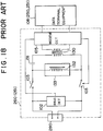
- FIG.1 shows an example of the conventional modem unit. In FIG.1, a
ring detection circuit 102 is connected to atelephone line 101 which connects to anexchange 100. Thering detection circuit 102 detects a calling signal from a remote end. Hook switches 103 respond to the on-hook/off-hook of the receiver. A line transformer 104 couples a primary side line (telephone line side) and the secondary line side (modem circuit side) with respect to the AC signal but provides a DC isolation between the two. - A
modem circuit 105 converts an analog signal into a digital signal, and converts a digital signal into an analog signal. Aninterface 106 on the side of the modem unit couples themodem circuit 105 and aninterface 107 of a dataterminal equipment 108. Theinterface 107 on the side of the dataterminal equipment 108 couples the dataterminal equipment 108 and theinterface 106 of the modem unit. - When the calling signal is input from the
exchange 100 via thetelephone line 101, thering detection circuit 102 operates and inputs the calling signal to themodem circuit 105. Themodem circuit 105 closes thehook switches 103 in response to the calling signal. The AC signal on the primary side line which is received from thetelephone line 101 is transmitted to the secondary side via theline transformer 104. Hence, the analog signal is converted into the digital signal in themodem circuit 105, and the digital signal is input to the dataterminal equipment 108 via theinterfaces - On the other hand, when transmitting data from the data
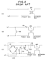
terminal equipment 108 to thetelephone line 101, themodem circuit 105 closes thehook switches 103 and makes a data transmission request with respect to the remote end. When the remote end answers, themodem circuit 105 converts the digital signal into the analog signal which is an AC signal, and this AC signal is transmitted to the primary side line via theline transformer 104. IN addition, this AC signal is transmitted to the remote end via thetelephone line 101. - Next, a description will be given of the transformer function of the conventional modem unit shown in FIG.1, by referring to FIG.2.
- FIG.2 (A) shows a case where a line transformer is used in the modem unit, and the illustration of other circuit parts is omitted. When a
line transformer 120 is used, all of the five demands described above are satisfied. - In other words, the DC loop is formed by the primary side line and the first demand is satisfied. the DC isolation between the primary side line and the secondary side line is achieved because the
line transformer 120 is used, and the second demand is satisfied. The transmission of the AC signal is achieved because theline transformer 120 is used, and the third demand is satisfied. The matching of the balanced and unbalanced signals can also be made since theline transformer 120 is used, and the fourth demand is satisfied. Furthermore, the noised elimination can be made and the fifth demand can be satisfied for the following reasons. - That is, the noise which is mixed on the telephone line in the transmission path is transmitted via two wires as in-phase signals, where the telephone line is made up of two wires L1 and L2. For this reason, the in-phase signals when input to the line transformer 120 causes magnetic fluxes to cancel each other, and the noise component will not be transmitted to the secondary side of the
line transformer 120. - Therefore, the
line transformer 120 can easily satisfy the demands with respect to the modem unit. However, there is a problem in that theline transformer 120 is bulky because of the need to flow a DC current which is necessary to capture the line. - Accordingly, it is possible to provide a DC current loop independently of the line transformer as shown in FIG.2 (B), so that no DC current flows to the line transformer.
- In FIG.2 (B), a
repeater transformer 130 does not supply a DC component to the primary side and transmits only the AC component to the secondary side. Acapacitor 131 is provided to cut off the DC component, and aloop coil 132 is provided to supply a DC current from the telephone line (L1, L2). - The
repeater transformer 130 also satisfies the first, third, fourth and fifth demands of the modem unit, similarly to theline transformer 120. In addition, the second demand of the modem unit is satisfied by theloop coil 132. - However, there is a problem in that the size of the
loop coil 132 cannot be reduced satisfactorily. - On the other hand, FIG.2 (C) shows a case where the DC current loop is formed by an active element. In a
pseudo inductance circuit 140 shown in FIG.2 (C), adiode bridge 141 is provided so that the polarity of the operating voltage of apseudo inductance 140 is maintained constant even if the polarity of the telephone line (L1, L2) is inverted. A capacitor C1 is provided to bypass the AC component so that the bias voltage of transistors TR1 and TR2 does not deviate by the AC component. Voltage dividing resistors R1 and R2 determine the bias voltage of the transistors TR1 and TR2. The transistors TR1 and TR2 form the DC current loop. An emitter resistance R3 forms the DC current loop together with the transistors TR1 and TR2. - A coupling capacitor C2 cuts off the DC voltage and passes only the AC component. In addition, a
repeater transformer 142 is provided. - By the DC voltage biasing, an approximately constant DC current flows through the transistors TR1 and TR2 and the resistance R3 without being affected by the AC component. On the other hand, the DC voltage is cut off by the capacitor C2 and only the AC component is supplied to the primary side of the
repeater transformer 142 and transmitted to the secondary side. - However, the conventional modem unit requires the line transformer, the repeater transformer, the loop coil or the like which are all bulky, and the size of the modem unit cannot be reduced satisfactorily. As a result, it is impossible to accommodate all circuit parts of the modem unit including the transformer within an IC card.
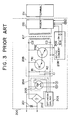
- FIG.3 shows another example of the conventional modem unit. A modem unit 200 basically corresponds to the modem unit shown in FIG.2 (C).
- In the modem unit 200 shown in FIG.3,
input protection elements 201 protect themodem unit 100 from a high impulse voltage caused by a lightening or the like. Adiode bridge 202 always maintains the polarity of the DC voltage which is applied to amodem circuit 210 constant even if the polarity of the DC voltage on the telephone line is inverted. An off-hook/dialing circuit 203 detects the off-hook and outputs a dial signal. Aring detection circuit 204 is made up of aphotocoupler 205, and detects the calling signal. Thephotocoupler 205 optically detects the calling signal. - A
pseudo inductance circuit 206 bypasses the DC current from the telephone line. Thepseudo inductance circuit 206 includes a capacitor C1, voltage dividing resistors R1 and R2, transistors TR1 and TR2, and coupling capacitors C2 and C3 for cutting off the DC current and passing the AC signal. - A line transformer 207 provides a DC isolation between the telephone line and a
terminal equipment 211, and transmits the AC signal. A DC/DC converter 208 shifts the DC voltage on the telephone line, and supplies the shifted voltage to amodem circuit 210 as a power source voltage. Atransformer 209 provides a DC isolation between theterminal equipment 211 and the telephone line. Themodem circuit 210 modulates the output digital signal of theterminal equipment 211 into the analog signal, and also demodulates the analog signal from the telephone line into the digital signal. - When a call is made from the remote end, the
ring detection circuit 204 is activated and the calling signal is detected by thephotocoupler 205. The detection of the calling signal is notified to themodem circuit 210. - On the other hand, the
pseudo inductance circuit 206 bypasses the DC current from the telephone line. In other words, the DC voltage is divided by the resistors R1 and R2 into the bias voltage of the transistors TR1 and TR2 which form a Darlington pair. The capacitor C1 presents the bias voltage of the transistor TR1 from deviating due to the AC component. Hence, an approximately constant current flows from the collector to the emitter of each of the transistors TR1 and TR2 regardless of the magnitude of the AC component. The DC current is cut off by the capacitors C2 and C3. For this reason, the DC current will not flow to the line transformer 207, and only the AC signal is input to the line transformer 207 and transmitted to themodem circuit 210. - The
modem circuit 210 converts the output digital signal of theterminal equipment 211 into the analog signal, and transmits this analog signal to the telephone line via the line transformer 207, the capacitors C2 and C3 and thepseudo inductance circuit 206. - On the other hand, the DC/
DC converter 208 subjects the DC voltage from the telephone line to a DC/DC conversion, and supplies the DC voltage to themodem circuit 210. Thetransformer 209 of the DC/DC converter 208 guarantees the DC isolation between the telephone line and theterminal equipment 211. - The off-hook/
dialing circuit 203 is made up of a photocoupler or the like, and transmits a dial signal by detecting an off-hook signal. - This modem unit 200 also uses the
line transformer 210 which is bulky. For example, theline transformer 210 has a height of approximately 10 mm. Therefore, the modem unit 200 including theline transformer 210 cannot be made in the form of an IC circuit. - Accordingly, it is a general object of the present invention to provide a novel and useful modem unit in which the problems described above are eliminated.
- Another and more specific object of the present invention is to provide a modem unit adapted to be coupled between a land or radio telephone line and a terminal equipment, comprising modem circuit means, coupled to the terminal equipment, for modulating data received from the terminal equipment and for demodulating data transmitted to the terminal equipment, and isolation means, coupled to the modem circuit means, for providing a DC isolation between the telephone line and the terminal equipment, where the modem circuit means and the isolation means are respectively provided on a single modem integrated circuit card. According to the modem unit of the present invention, the entire modem unit is provided on the single modem integrated circuit card, thereby making it extremely convenient to carry the modem unit.
- Still another object of the present invention is to provide the modem unit described above wherein the isolation means includes capacitor means, coupled to the telephone line, for cutting off a DC current from the telephone line and for passing an AC signal from the telephone line, and the modem unit further comprises a first differential circuit having a non-inverting input terminal which receives a received signal from one wire of the telephone line via the capacitor means, an inverting input terminal which receives a received signal from the other wire of the telephone line via the capacitor means, and an output terminal which supplies an output analog signal to the modem circuit means wherein the analog signal is converted into a digital signal which is transmitted to the terminal equipment, and a second differential circuit having an input terminal which receives a digital signal which originates from the terminal equipment and is converted into an analog input signal in the modem circuit means, and a pair of output terminals which supply an analog signal having a polarity inverted with respect to the analog input signal and an analog signal having the same polarity as the analog input signal to the telephone line via the capacitor means. According to the modem unit of the present invention, no transformer is required.
- A further object of the present invention is to provide the modem unit of the type described first above wherein the isolation means includes photocoupler means for optically exchanging signals between the modem circuit means and the terminal equipment. According to the modem unit of the present invention, no transformer is necessary.
- Another object of the present invention is to provide the modem unit of the type described first above wherein the modem integrated circuit card has a shape and size which are approximately the same as those of a memory integrated circuit card which is provided with a slot through which a battery of the memory integrated circuit card is replaceable, and the modem integrated circuit card includes connecting means, provided at a predetermined position corresponding to that of the slot of the memory integrated circuit card, for coupling the modem unit to the telephone line. According to the modem unit of the present invention, it is possible to load the modem unit into the terminal equipment without the need to modify the construction of the terminal equipment which is designed to accept the existing memory integrated circuit card.
- Still another object of the present invention is to provide the modem unit of the type described first above which further comprises network control means having terminals for coupling to the telephone line, and connector means having first terminals for coupling to the telephone line, the first terminals being coupled to the terminals of the network control means, where the isolation means includes hybrid circuit means for coupling the telephone line and the modem circuit means with respect to an AC signal. According to the modem unit of the present invention, it is possible to arbitrarily connect the modem unit to the land telephone line or the radio telephone line by use of the connector means.
- A further object of the present invention is to provide the modem unit described immediately above wherein the connector means further includes second terminals coupled to the modem circuit means.
- Another object of the present invention is to provide the modem unit described above having the connector means, wherein the connector means further includes a pair of second terminals which are coupled to the hybrid circuit means and a third terminal which is coupled to the network control means, the second and third terminals are connectable to an external unit, and one of the second terminals and the third terminal are short-circuited when no external unit is coupled to the modem unit.
- Still another object of the present invention is to provide the modem unit of the type described first above which further comprises a battery for supplying power to various parts of the modem unit, detection means, coupled to the battery, for detecting an output voltage level of the battery, and selection means, coupled to the detection means, for selecting a frequency of a clock which drives the modem circuit means depending on the voltage level detected by the detection means, where the modem circuit means includes determination means, coupled to the detection means, for determining a modem function of the modem circuit means based on the voltage level detected by the detection means and function request information specified from the terminal equipment. According to the modem unit of the present invention, it is possible to automatically continue the data communication even if the voltage level of the battery falls, by reducing the clock frequency and reducing the modem functions.
- Other objects and further features of the present invention will be apparent from the following detailed description when read in conjunction with the accompanying drawings.
-
- FIG.1 is a system block diagram showing an example of a conventional modem unit;
- FIG.2 in parts (A) through (C) show circuit diagrams for explaining the transformer function of the conventional modem unit;
- FIG.3 is a system block diagram showing another example of the conventional modem unit;
- FIG.4 is a system block diagram for explaining the operating principle of a first embodiment of a modem unit according to the present invention;
- FIG.5 is a system block diagram showing the first embodiment;
- FIG.6 is a system block diagram for explaining the operating principle of a second embodiment of the modem unit according to the present invention;
- FIGS.7 and 8 are system block diagrams respectively showing the second embodiment;
- FIG.9 is a perspective view showing an IC card which is loaded into a portable data processing unit;
- FIG.10 is a perspective view showing the IC card;
- FIG.11 is a perspective view for explaining the replacement of a battery of the IC card;
- FIG.12 is a perspective view showing a modem IC card which is loaded into the portable data processing unit;
- FIG.13 is a perspective view showing the modem IC card;
- FIG.14 is a perspective view showing a third embodiment of the modem unit according to the present invention which is loaded into the portable data processing unit;
- FIG.15 is a perspective view showing the third embodiment;
- FIG.16 is a perspective view showing a modification of the third embodiment together with a connector;
- FIG.17 is a diagram for explaining a data communication system using modem units;
- FIG.18 is a system block diagram showing an example of the conventional modem unit used in the data communication system shown in FIG.17;
- FIG.19 is a system block diagram for explaining the operating principle of a fourth embodiment of the modem unit according to the present invention;
- FIG.20 is a diagram for explaining a data communication system using the fourth embodiment;
- FIG.21 shows an embodiment of a connecting cable which connects to a telephone line in the fourth embodiment;
- FIG.22 shows an embodiment of a connecting cable which is connectable to the telephone line and a mobile telephone in the fourth embodiment;
- FIG.23 is a circuit diagram showing an embodiment of a NCU shown in FIG.19;
- FIG.24 is a circuit diagram showing an embodiment of a hybrid circuit shown in FIG.19;
- FIG.25 is a system block diagram showing an essential part of a fifth embodiment of the modem unit according to the present invention;
- FIG.26 shows an embodiment of a connecting cable used in the fifth embodiment;
- FIG.27 is a system block diagram showing a conceivable modem unit which is connectable to an external unit;
- FIG.28 in parts (A) and (B) shows an essential part of a sixth embodiment of the modem unit according to the present invention;
- FIG.29 in parts (A) and (B) shows an essential part of a seventh embodiment of the modem unit according to the present invention for explaining the operation principle thereof;
- FIG.30 in parts (A) and (B) shows the seventh embodiment in more detail;
- FIG.31 is a system block diagram showing an essential part of an eighth embodiment of the modem unit according to the present invention;
- FIG.32 is a system block diagram showing an essential part of a ninth embodiment of the modem unit according to the present invention;
- FIG.33 is a circuit diagram showing a tenth embodiment of the modem unit according to the present invention;
- FIG.34 is a circuit diagram showing an eleventh embodiment of the modem unit according to the present invention;
- FIG.35 is a system block diagram showing a twelfth embodiment of the modem unit according to the present invention;
- FIG.36 is a system block diagram for explaining the problems of a conventional battery-operated modem unit;
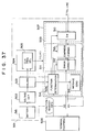
- FIG.37 is a system block diagram for explaining the operating principle of thirteenth and fourteenth embodiments of the modem unit according to the present invention;
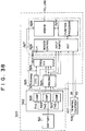
- FIG.38 is a system block diagram showing the thirteenth embodiment;
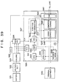
- FIG.39 is a system block diagram showing an embodiment of a modem processor of the thirteenth embodiment;
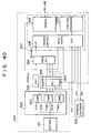
- FIG.40 is a system block diagram showing the fourteenth embodiment; and
- FIG.41 is a system block diagram showing an embodiment of the modem processor of the fourteenth embodiment.
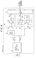
- First, a description will be given of the operating principle of a first embodiment of a modem unit according to the present invention, by referring to FIG.4.
- A
modem unit 1 shown in FIG.4 generally includes apseudo inductance circuit 2, capacitors C1 and C2, a send signal cut off circuit 5,differential circuits modem circuit 8. For example, thepseudo inductance circuit 2 has the same construction as thepseudo inductance circuit 140 shown in FIG.2 (C). The capacitors C2 and C3 cut off the DC current from a telephone line and pass only the AC signal. The send signal cut off circuit 5 prevents a send signal of themodem unit 1 from being input to a reception circuit thereof at the time of a transmission. - The
differential circuit 6 receives one of analog balanced received signals output from thepseudo inductance circuit 2 to an inverting input terminal and the other to a non-inverting input terminal, and outputs analog unbalanced received signals. Thedifferential circuit 7 receives analog unbalanced signals which are subjected to the digital-to-analog (D/A) conversion in themodem circuit 8, and outputs complementary output signals. In other words, a signal which is inverted with respect to the input signal is output from one output terminal of thedifferential circuit 7, and a signal having the same polarity as the input signal is output from the other output terminal of thedifferential circuit 7. - The
modem circuit 8 demodulates the analog received signal into the digital signal and supplies this digital signal to a data terminal equipment (not shown). In addition, themodem circuit 8 modulates the output digital signal of the data terminal equipment into the analog signal and supplies the analog signal to the telephone line. - The
differential circuit 6 has anon-inverting input terminal 10, an invertinginput terminal 10, and anoutput terminal 14 for outputting the received signal. In this particular case, thedifferential circuit 6 is made up of anoperational amplifier 16. On the other hand, thedifferential circuit 7 has an invertingoutput terminal 12, anon-inverting output terminal 13, and aninput terminal 15 for receiving the send signal. In this particular case, thedifferential circuit 7 is made up ofoperational amplifiers - Next, a description will be given of the operation of the
modem unit 1. The DC current from the telephone line is cut off by the capacitors C1 and C2 and will not be input to thedifferential circuits - When making a reception, the AC signal component from the telephone line is input to the
differential circuit 6 via thepseudo inductance circuit 2 and the capacitors C1 and C2. The received signal is essentially made up of balanced signals. Hence, the signal from the capacitor C1 is input to thenon-inverting input terminal 10 of thedifferential circuit 6, and the signal from the capacitor C2 is input to the inverting input terminal 11 of thedifferential circuit 6. The polarity of the signal input to the inverting input terminal 11 is inverted using the input signal to thenon-inverting input terminal 10 as a reference voltage, and is output from theoutput terminal 14. Accordingly, thedifferential circuit 6 outputs the input balanced signals as unbalanced signals. - On the other hand, when making a transmission, the
modem circuit 8 converts the output digital signal of the data terminal equipment into the analog signal which is essentially made up of unbalanced send signals. For example, the send signal is input to the inverting input terminal of theoperational amplifier 17 within thedifferential circuit 7, and the polarity-inverted signal is output from the invertingoutput terminal 12. In addition, the output signal of theoperational amplifier 17 is input to the inverting input terminal of theoperational amplifier 18, and the polarity-inverted signal is output from thenon-inverting output terminal 13 as a signal having the same polarity as the signal input to theinput terminal 15. A reference voltage VREF is input to the non-inverting input terminals of theoperational amplifiers operational amplifiers pseudo inductance circuit 2 as balanced signals. - Of course, the constructions of the
differential circuits - Next, a description will be given of the first embodiment, by referring to FIG.5. In FIG.5, those parts which are the same as those corresponding parts in FIG.4 are designated by the same reference numerals, and a description thereof will be omitted.
- In FIG.5, the telephone line is made up of two wires L1 and L2. A resistor R11 together with a resistor R16 determines the reference voltage which is input to the non-inverting input terminal of the
operational amplifier 16 which forms thedifferential circuit 6, based on the AC component which is input from the wire L1. A resistor R12 together with a resistor R17 determines the amplification of theoperational amplifier 16 with respect to the AC component which is input from the wire L2. The resistor R17 forms a negative feedback resistance of theoperational amplifier 16. Resistors R13 and R14 determine the impedance of the modem unit with respect to the AC component. - A resistor R15 prevents the send signal of the modem unit from being input to the
differential circuit 6 as a received signal at the time of the transmission. A resistor R18 forms a negative feedback resistance of theoperational amplifier 17, and determines the amplification of theoperational amplifier 17 together with a resistor R19. A resistor R20 is provided to stabilize the operation of theoperational amplifier 18. A resistor R21 forms a negative feedback resistance of theoperational amplifier 18, and determines the amplification of theoperational amplifier 18 together with a resistor R22. - When making a reception, a substantially balanced transmission takes place on the telephone line. For example, a send signal a having the waveform shown in FIG.5 is output from the capacitor C1, and a signal b is having the waveform shown in FIG.5 is output from the capacitor C2. In this case, a signal c having the waveform shown is output from the
operational amplifier 16. The signal a is input to the non-inverting input terminal of theoperational amplifier 16 as the reference voltage. The signal b input to the inverting input terminal of theoperational amplifier 16. Hence, the output signal c of theoperational amplifier 16 is inverted relative to the signal b. In other words, the signal c is output based on the balanced signals a and b input to theoperational amplifier 16. - On the other hand, when making a transmission, a send signal d having the waveform shown in FIG.5, for example, is input to the
differential circuit 7. This send signal d is input to the non-inverting input terminal of theoperational amplifier 17. As a result, a signal e having the same phase as the signal d is output from theoperational amplifier 17. On the other hand, this output signal e of theoperational amplifier 17 is input to the inverting input terminal of theoperational amplifier 18. Hence, a signal f is output from theoperational amplifier 18. The output signals e and f of thedifferential circuit 7 are transmitted to the telephone line as balanced signals via the capacitors C1 and C2 and thepseudo inductance circuit 2. - In addition, an appropriate amount of the send signal e is applied to the inverting input terminal of the
operational amplifier 16 via the resistor R15. As a result, the signal f which is applied to the inverting input terminal of theoperational amplifier 16 via the resistors R14 and R12 and the signal e which is applied to the non-inverting input terminal of theoperational amplifier 16 via the resistors R13 and R11 cancel each other, so that essentially no send signal is input to thedifferential circuit 6. Therefore, it is possible to prevent the send signal from being input to the modem unit as a received signal at the time of the transmission. - According to this first embodiment, the transformer function and the loop coil function with respect to the DC current are realized by active circuits including no transformer. For this reason, it is possible to make the entire modem unit in the form of an IC, and the modem unit as a whole can be made thin. In other words, it is possible to accommodate the entire modem unit within an IC card.
- Next, a description will be given of the operating principle of a second embodiment of the modem unit according to the present invention, by referring to FIG.6.
- In FIG.6, a
modem unit 21 includes adiode bridge 22, aring detection circuit 23, a dialingcircuit 24, apseudo inductance circuit 25, an ACsignal transmitting circuit 26, amodem circuit 27, apolarity detection circuit 28, a DC/DC converter 29, apower unit 31, apower switch 32, aprotection diode circuit 33, and amodem interface 34. - The
ring detection circuit 23 is made up of voltage dividing resistors Ra and Rb, and detects a call from the remote end based on the divided voltage. The ACsignal transmitting circuit 26 is made up of active circuits having a transformer function without the use of a transformer, and transmits an analog signal between the telephone line and themodem circuit 27, where the telephone line is made up of wires L1 and L2. Themodem circuit 27 demodulates an analog signal into a digital signal, and modulates a digital signal into an analog signal. - The
polarity detection circuit 28 is made up of voltage dividing resistors Rc and Rd and detects the polarity inversion on the telephone line. The DC/DC converter 29 subjects the DC voltage on the telephone line to a DC/DC conversion and supplies the output voltage to themodem circuit 27 as a power source voltage. Thepower unit 31 is made up of a battery, for example, and supplies the power source voltage to themodem circuit 27 in a state where themodem circuit 27 and the telephone line are not connected. Thepower switch 32 switches and selects the output power source voltage of thepower unit 31 or the DC/DC converter 29. - The
modem interface 34 exchanges signals between themodem circuit 27 and aterminal interface 36 of aterminal equipment 35. Themodem interface 34 is made up of photocouplers 34' and 34''. - The
diode bridge 22 prevents the polarity of the DC voltage which is applied to themodem circuit 27 from changing even if the polarity of the DC voltage on the telephone line is inverted. - When a call is received from the remote end, a divided voltage is generated by the voltage dividing resistors Ra and Rb of the
ring detection circuit 23, and this divided voltage is input to a ring voltage input terminal RING of themodem circuit 27. Theprotection diode circuit 33 protects themodem unit 21 from an excessively large input, so that a voltage greater than 5 V will not be input to the ring voltage input terminal RING. - The DC/
DC converter 29 subjects the DC voltage from the telephone line to the DC/DC conversion. Thepower switch 32 detects an off-hook signal OH from themodem circuit 27, and switches the power source voltage which is supplied to themodem circuit 27 from the output power source voltage of thepower unit 31 to the output power source voltage of the DC/DC converter 29 in response to the detection of the off-hook signal OH. - The AC
signal transmitting circuit 26 includes coupling capacitors for cutting off the DC current from the telephone line and for passing the AC signal, and differential circuits. The ACsignal transmitting circuit 26 converts the balanced signals from the telephone line into unbalanced signals. In addition, the ACsignal transmitting circuit 26 converts the unbalanced signals from themodem circuit 27 into balanced signals, and transmits the balanced signals to the wires L1 and L2 which form the telephone line. - The
modem interface 34 exchanges signals between theterminal equipment 35 and themodem circuit 27. The photocoupler 34' transmits the signal from themodem circuit 27 to theterminal equipment 35. On the other hand, the photocoupler 34'' transmits the signal from theterminal equipment 35 to themodem circuit 27. - The
modem circuit 27 converts a transmitting digital signal into an analog signal and supplies the analog signal to the ACsignal transmitting circuit 26. In addition, themodem circuit 27 converts a received analog signal from the ACsignal transmitting circuit 26 into a digital signal and supplies this digital signal to theterminal equipment 35 via themodem interface 34. - Because the
modem interface 34 provides a DC isolation between theterminal equipment 35 and themodem circuit 27, thepolarity detection circuit 28 may have a simple construction made up of the voltage dividing resistors Rc and Rd. In other words, thepolarity detection circuit 28 detects the polarity change of the DC voltage on the telephone line by detecting the change of the divided voltage generated by the voltage dividing resistors Rd and Rd. - In a personal computer communication typified by the CCITT Recommendations V.22bis, the answer from the remote end is made by transmitting a signal from the remote end. For this reason, it is not essential to provide the
polarity detection circuit 28. - The dialing
circuit 24 and thepseudo inductance circuit 25 may have the same construction as those of the conventional modem unit shown in FIG.3, for example. Hence, a description thereof will be omitted. - According to this second embodiment, the
terminal equipment 35 and themodem unit 21 are coupled via themodem interface 34, that is, via the photocouplers 14' and 14''. For this reason, the DC isolation between themodem unit 21 and theterminal equipment 35 is complete. As a result, themodem unit 21 does not require the means for realizing the power unit isolation between the telephone line and theterminal equipment 35 as in the conventional case so as to guarantee the DC withstand voltage of 250 V or greater and an isolation resistance of 0.2 MOhms or greater, for example. Consequently, thepolarity detection circuit 28 and thering detection circuit 23 can be formed by the resistors Ra, Rb, Rc and Rd and theprotection diode circuit 33, thereby eliminating the need to use the photocoupler which is conventionally used. The illustration of a protection diode circuit for maintaining the output voltage of thepolarity detection circuit 28 within a predetermined range is omitted in FIG.6. - Similarly to the reasons described above, the transformer conventionally required in the DC/
DC converter 29 can be eliminated in this embodiment. Furthermore, the coupling of the telephone line and themodem circuit 27 with respect to the AC signal is made by the ACsignal transmitting circuit 26 which uses differential circuits and capacitors to realize the functions of the conventional line transformer. This means that the line transformer can be eliminated, thereby making it easy to make theentire modem unit 21 in the form of an IC card. - Next, a more detailed description will be given of the second embodiment, by referring to FIGS.7 and 8. Terminals B, C, D, E, F, H and I shown in FIG.7 respectively connect to the corresponding terminals B, C, D, E, F, H and I shown in FIG.8. In FIGS.7 and 8, those parts which are the same as those corresponding parts in FIG.6 are designated by the same reference numerals, and a description thereof will be omitted.
- In FIG.7,
input protection elements 20 protect the modem unit from a high impulse voltage caused by lightning or the like. Thering detection circuit 23 is made up of voltage dividing resistors R31 and R32. A buffer B1 inputs the ring detection voltage from thering detection circuit 23 to themodem circuit 27. Theprotection diode circuit 33 is made up of diodes D1 and D2, and protects the buffer B1. The dialingcircuit 24 is made up of a photo MOS relay 24' and outputs the dial signal. Thepolarity detection circuit 28 is made up of voltage dividing resistors R34, R35, R36 and R37 for detecting the voltage polarity on the telephone line, and outputs the polarity detection voltage. Diodes D3, D4, D5 and D6 are provided to maintain the polarity detection voltage within a predetermined range so that buffers B2 and B3 are protected. The buffers B2 and B3 input the polarity detection voltage to themodem circuit 27. - In FIG.8, the AC
signal transmitting circuit 26 includesdifferential circuits differential circuit 31 is made up of an operational amplifier 31'. Thedifferential circuit 32 is made up of operational amplifiers 32' and 32''. The input protection diodes D11 and D12 protect the operational amplifiers 31', 32' and 32'' from an excessively large input voltage. The resistor R38 prevents the send signal from the terminal equipment (not shown) from being fed back to the terminal equipment. - The
modem interface 34 includesphotocouplers - The
modem circuit 27 is provided with analog signal output terminals L1 and L2, a power source voltage input terminal VCC, a ground terminal GND, an off-hook signal output terminal *OH, a ring detection signal input terminal *RING, polarity detection voltage input terminals *RVS1 and *RVS2, an equipment ready signal input terminal *ER, a request to send signal input terminal *RS, a send signal input terminal SD, a received signal output terminal RD, a clear to send signal output terminal *CS, and a data set ready signal output terminal *DR. The symbol "*" indicates negative logic. - The off-hook signal output terminal *OH outputs the off-hook signal which turns ON by an off-hook and turns OFF by an on-hook. The equipment ready signal input terminal *ER receives the equipment ready signal from the terminal equipment indicating the receivable state of the terminal equipment. The request to send signal input terminal *RS receives request to send signal from the terminal equipment. The send signal input terminal SD receives the send signal from the terminal equipment. The clear to send signal output terminal *CS outputs the clear to send signal to the terminal equipment. The data set ready signal output terminal *DR outputs the data set ready signal to the terminal equipment to notify the ready state of the modem unit.
- The symbols used for the inputs and outputs of the
modem interface 34 are the same as those used for the input and output terminals of themodem circuit 27. - Next, a description will be given of the operation of the circuit shown in FIGS.7 and 8.
- When making the dialing, the off-hook signal *OH is turned ON and the dialing
circuit 24 outputs the dial signal to the telephone line (L1, L2) via the photo MOS relay 24'. - On the other hand, when making the dialing according to a different system, the off-hook signal *OH is first turned ON and a DTMF signal is thereafter output to the telephone line (L1, L2) from the
modem circuit 27. - The
ring detection circuit 23 operates as follows. That is, when a ringing voltage is input from the telephone line, an AC signal having a maximum of 83 Vrms is applied across thediode bridge 22. The output voltage of thediode bridge 22 is divided by the resistors R31 and R32 of thering detection circuit 23, so as to obtain a voltage in a range of 0 to 5 V. Furthermore, the voltage range is guaranteed by the diodes D1 and D2 of theprotection diode circuit 33. The ring detection signal is thus input to the ring detection signal input terminal *RING of themodem circuit 27 via the buffer B1. - The
polarity detection circuit 28 operates as follows. That is, when the polarity on the telephone line is inverted at the exchange (not shown), a potential difference between the wires L1 and L2 of the telephone line changes from +48 V to -48 V. This voltage change is obtained via the resistors R33 through R36, and the voltage range is guaranteed by the protection diodes D3 through D6. Thus, the polarity detection voltages are input to the polarity detection voltage input terminals *RVS1 and *RVS2 of themodem circuit 27 via the buffers B2 and B3. - The voltage dividing resistors R31 and R32 of the
ring detection circuit 23 and the voltage dividing resistors R33 through R36 of thepolarity detection circuit 28 are set sufficiently large so as to satisfy the standards of the telephone line. - The operation of the DC/
DC converter 29 and thepower switch 32 is the same as that described with reference to FIG.6. In addition, the operation of theinput protection elements 20, thediode bridge 22 and thepseudo inductance circuit 25 is the same as that of the circuit shown in FIG.3, for example. - Next, a description will be given of the operation of the
modem interface 34 and themodem circuit 27. - The following processes are carried out when the terminal equipment transmits the data.
- [1] The equipment ready signal *ER which indicates that the terminal equipment is ready is received from the terminal equipment. This equipment ready signal *ER is input to the
modem circuit 27 via thephotocoupler 40. - [2] The
modem circuit 27 outputs the data set ready signal *DR which indicates that themodem circuit 27 is ready. This data set ready signal *DR is supplied to the terminal equipment via thephotocoupler 45. - [3] The terminal equipment transmits the request to send signal *RS. This request to send signal *RS is input to the
modem circuit 27 via thephotocoupler 41. Themodem circuit 27 supplies a carrier wave on the telephone line in response to the request to send signal *RS. The modem circuit (not shown) on the receiving end detects the data from the carrier wave. - [4] The
modem circuit 27 transmits the clear to send signal *CS to the terminal equipment via thephotocoupler 44. - [5] The terminal equipment transmits the send data SD in response to the clear to send signal *CS from the
modem circuit 27. The send data SD is input to themodem circuit 27 via thephotocoupler 42, and is converted into an analog signal which is transmitted to the telephone line. - On the other hand, the following processes are carried out when receiving the data from the telephone line.
- That is, the
modem circuit 27 converts the received analog signal into a digital signal. This digital signal is transmitted to the terminal equipment via thephotocoupler 43 as the received data RD. - Next, a description will be given of the operation of the AC
signal transmitting circuit 26. - The transmission can be regarded as being essentially balanced on the telephone line, and thus, the polarities of the signals passing through the capacitors C10 and C11 are opposite to each other. For example, if a sending signal a shown in FIG.8 passes through the capacitor C10, it will be assumed for the sake of convenience that a signal b is output from the capacitor C12, and that the operational amplifier 31' outputs a signal c.
- The sending signal a is input to the non-inverting input terminal of the operational amplifier 31' as a reference voltage. The signal b is input to the inverting input terminal of the operational amplifier 31'. As a result, the signal c which is an inverted signal of the signal b is output from the operational amplifier 31'. This signal c is input to the
modem circuit 27 as an unbalanced signal. - It will be assumed for the sake of convenience that a send signal d shown in FIG.8 is output from the
modem circuit 27. This send signal d is input to the non-inverting input terminal of the operational amplifier 32'. As a result, a signal e having the same phase as the signal d is output from the operational amplifier 32'. In addition, the output signal e of the operational amplifier 32' is input to the inverting input terminal of the operational amplifier 32''. Thus, a signal f which is an inverted signal of the signal d is output from the operational amplifier 32''. The signals e and f are output to the telephone line via the capacitors C10 and C11 and thepseudo inductance circuit 25 as balanced signals. - In addition, the send signal f is input to the operational amplifier 31' via the resistor R38 so as to prevent the send signal f from being fed back and output from the operational amplifier 31'.
- In the
modem interface 34, thephotocouplers 40 through 45 couple the terminal equipment and themodem circuit 27. But if no DC isolation were provided, the capacitors C10 and C11 would need to have a DC withstand voltage of 250 V and an isolation resistance of 0.2 MOhms or greater in order to satisfy the standards. The capacitors C10 and C11 would then become relatively large so as to meet the withstand voltage requirement. However, the capacitors C10 and C11 simply need to withstand the DC voltage on the telephone line in this embodiment because thephotocouplers 40 through 45 are used, and the capacitors C10 and C11 can be made small. - Therefore, according to this embodiment, the modem unit does not include a transformer such as the line transformer, and there is no direct coupling between the power unit part of the modem unit and the terminal equipment. Hence, it is unnecessary to take into consideration the withstand voltage with respect to the power unit part.. Consequently, the modem unit as a whole can be made small, and the entire modem unit can be made in the form of an IC card.
- Next, a description will be given of a general IC card.
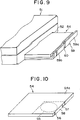
- FIG.9 shows an IC card which is inserted into a portable data processing unit such as a portable personal computer. The portable data processing unit is made up of a
unit body 51 having aloading opening 52 on a side of theunit body 51. Various kinds of IC cards can be loaded into the portable data processing unit via theloading opening 52. - FIG.10 shows an example of the IC card which can be loaded into the portable data processing unit. A SRAM (or memory)
card 54 accommodates abattery 55 for preserving stored data. In order to make thebattery 55 replaceable, thememory card 54 is provided with abattery changing slot 56. This changingslot 56 is normally closed by alid 58 which is secured on acard body 54a by ascrew 57. - In order to preserve the memory contents, the
battery 55 must be changed in a state where thememory card 54 is loaded into the portable data processing unit, that is, in a state where the power is supplied to thememory card 54 from the portable data processing unit. As shown in FIG.11, thelid 58 is removed in the state where thememory card 54 is loaded into the portable data processing unit via theloading opening 52 when replacing thebattery 55. - On the other hand, a
lid member 59 is provided on theunit body 51 so that thememory card 54 is not exposed to the outside in the loaded position and so that theloading opening 52 is not exposed to the outside when nomemory card 54 is loaded. Thislid member 59 closes theloading opening 52. - This
lid member 59 is made up of abody part 59a having anopening 60 for enabling the battery replacement, and adetachable lid 59b which normally closes theopening 60. The position of theopening 60 is approximately the same among the various memory cards because the position where the battery is accommodated is approximately unified. When removing thebattery 55, thelid 59b is removed, and thescrew 57 is loosened so as to remove thelid 58. - FIG.12 shows a
modem IC card 65 which is loaded into the loading opening 52 of theunit body 51. In FIG.12, those parts which are the same as those corresponding parts in FIG.9 are designated by the same reference numerals, and a description thereof will be omitted. - As shown in FIGS.12 and 13, the
modem IC card 65 is provided with an external connectingpart 53 at a central part along the side of themodem IC card 65. The external connectingpart 53 may be a cable, a connector or the like. Themodem IC card 65 has an external shape and size which are approximately the same as those of the existingmemory card 54. - If the modem IC card is loaded into the
unit body 51 via theloading opening 52, the external connectingpart 53 will hit thelid member 59. For this reason, it is necessary to use themodem IC card 65 in a state where thelid member 59 is removed from theunit body 51. But the removal of thelid member 59 will damage the external appearance of theunit body 51. - In order to eliminate this problem, it is conceivable to provide a special lid member 59' exclusively for use with the
modem IC card 65. However, themodem IC card 65 is in most cases an optional feature of the portable data processing unit, and the need to provide this special lid member 59' would increase the cost of the system. - Next, a description will be given of a third embodiment of the modem unit according to the present invention. In this embodiment, the entire modem unit is made in the form of an IC card, and will be referred to as a modem IC card. For example, the modem unit itself may have the structure of the first or second embodiment described above.
- FIG.14 shows this embodiment of the modem unit, that is, a
modem IC card 66, which is loaded into theunit body 51 of the portable data processing unit. FIG.15 shows themodem IC card 66. - The
unit body 51 of the portable data processing unit has theloading opening 52, and thelid member 59 for normally closing theloading opening 52, as shown in FIG.14. Thelid member 59 is made up of thebody part 59a and thedetachable lid 59b. Theopening 60 for enabling thebattery 55 of thememory card 54 to be replaced is normally closed bydetachable lid 59b. - In the loaded position of the above described
memory card 54 within theunit body 51, theloading opening 52 is closed by thelid member 59 which is fitted with thelid 59b. Hence, thebattery 55 of thememory card 54 can be replaced as described above in conjunction with FIG.11, that is, by first removing thelid 59b and thereafter removing thelid 58 of thememory card 54. - On the other hand, unlike the
memory card 54, themodem IC card 66 has an external connecting part (cable) 53 which extends from the side of themodem IC card 66. A receptacle (not shown) is provided on a tip end of the external connectingcable 53, and connects to the telephone line or a mobile telephone, for example. This external connectingcable 53 is arranged at a position corresponding to the position of thelid 59b, that is, the part of thelid member 59 where theopening 60 is provided. In addition, the diameter of the external connectingcable 53 is such that the external connectingcable 53 completely fits within theopening 60. - Accordingly, when loading the
modem IC card 66 into the portable data processing unit, thelid member 59 is once pulled out of theunit body 61, and thelid 59b is removed. Then, themodem IC card 66 is placed on thelid member 59. In this state, the external connectingcable 53 completely fits within theopening 60 of thelid member 59 as shown in FIG.14, and will not hit thebody part 59a of thelid member 59. Thereafter, thelid member 59 is pushed into theunit body 51 so as to complete the loading operation. - In other words, by arranging the external connecting
cable 53 at the position corresponding to theopening 60 of thelid member 59, it becomes unnecessary to use the special lid member 59' shown in FIG.12. Because the position of theopening 60 is approximately the same among the existing memory cards, this embodiment enables compatible use of themodem IC card 66 with the portable data processing unit having thelid member 59. - FIG.16 shows a modification of the third embodiment together with a connector 61a. In the case of the
modem IC card 66 shown in FIG.15, the external connectingcable 53 is connected directly on the side of themodem IC card 66. However, in this modification, a connector 61a is provided on a tip end of an external connectingcable 61, and amodem IC card 66A is provided with aconnector 63 for receiving the connector 61a. The size of the connector 61a is slightly smaller than theopening 60 of thelid member 59, so that the connector 61a completely fits within theopening 60 in a state where the connector 61a is connected to theconnector 63 of themodem IC card 66A. The connector 61a can be connected to and disconnected from theconnector 63 of themodem IC card 66A in the state where themodem IC card 66A is loaded into theunit body 51. - According to the third embodiment and the modification thereof, it is possible to effectively utilize the opening which is provided in the lid member for enabling battery replacement of the memory card, so that the external connecting part (cable) can be drawn outside from the modem IC card via the opening in the lid member without the need for a specially designed lid member exclusively for the modem IC card.
- Next, a description will be given of the problems of the modem unit which is provided independently of the data processing unit, by referring to FIGS.17 and 18.
- A data communication system shown in FIG.17 includes a transmitting end and a receiving end which are coupled via a
telephone line 255. The transmitting end includes apersonal computer 250, and amodem unit 260 coupled between thepersonal computer 250 and thetelephone line 255. On the other hand, the receiving end includes apersonal computer 251, and amodem unit 261 coupled between thepersonal computer 251 and thetelephone line 255. For example, thepersonal computers - The
modem unit 260 converts the output digital data of thepersonal computer 250 into an analog signal, and transmits the analog signal to the receiving end via thetelephone line 255. Themodem unit 261 converts the analog signal which is received from thetelephone line 255 into a digital signal, and supplies the digital signal to thepersonal computer 251. - FIG.18 shows the construction of the
modem unit 260. The construction of themodem unit 261 is identical to that of themodem unit 260, and a description thereof will be omitted. In FIG.18, those parts which are the same as those corresponding parts in FIGS.1 and 2 (B) are designated by the same reference numerals, and a description thereof will be omitted. - A
connector 280 connects to thetelephone line 255. However, if the data communication is to be made via radio, it is necessary to connect the modem unit 260 (or 261) to a mobile telephone (not shown) and to the personal computer 250 (or 251). But since therepeater transformer 130, aDC loop circuit 133 including theloop coil 132 and the like of the modem unit 260 (or 261) are bulky and cannot be built into a modem IC card, it is inconvenient in that the user must carry not only the mobile telephone but also the modem IC card and the bulky remaining portion of the modem unit 260 (or 261). In addition, the bulky remaining portion of the modem unit 260 (or 261) is relatively heavy compared to the wire portion, and undesirable stress is generated at the connecting part particularly if the bulky remaining portion simply hangs from the personal computer 250 (or 251) which is set on an end of a table, for example. Furthermore, it requires at least two connecting cables to connect the bulky remaining portion of the modem unit 260 (or 261) to the telephone line and to the personal computer 250 (or 251). - Next, a description will be given of the operating principle of a fourth embodiment of the modem unit according to the present invention, by referring to FIG.19. According to this embodiment, the entire modem unit is built into the modem IC card by the use of a hybrid circuit in place of the line transformer or the like, and a connector is designed so as to facilitate the data communication when connecting the modem IC card to the personal computer and the mobile telephone.
- In FIG.19, a
modem IC card 71 includes aconnector 73, a network control unit (NCU) 80, capacitors C1 and C2, ahybrid circuit 84, and amodem circuit 85. TheNCU 80 includes aring detection circuit 81, aDC loop circuit 83, ahook switch 82 and the like. TheDC loop circuit 83 is made up of active elements and a pseudo inductance circuit which is made up solely of passive elements. Thehybrid circuit 84 is made up of active elements and a circuit which is made up solely of passive elements. TheNCU 80, thehybrid circuit 84 and themodem circuit 85 are respectively made in the form of ICs. - On the other hand, a
mobile telephone 72 includes an antenna 72' and a connector 75''. Themodem IC card 71 and themobile telephone 72 are coupled via a connectingcable 74. The connectingcable 74 has a connector 73' which connects to theconnector 73 of themodem IC card 71, and a connector 75' which connects to the connector 75'' of themobile telephone 72. - The connector 73' has terminals A, B, C, D and E which connect to corresponding terminals A, B, C, D and E of the
connector 73 of themodem IC card 71. The connector 75' has send/receiveterminals 75 which connect to corresponding send receiveterminals 75 of themobile telephone 72. More particularly, the send/receiveterminals 75 of the connector 75'' include a microphone input terminal 75-1, that is, a send signal input terminal 75-1 of themobile telephone 72, and an earphone output terminal 75-2, that is, a received signal output terminal 75-2 of themobile telephone 72. - FIG.20 shows a communication system applied with the fourth embodiment. In FIG.20, those parts which are the same as those corresponding parts in FIG.17 are designated by the same reference numerals, and a description thereof will be omitted.
- In FIG.20, the transmitting end includes the
personal computer 250, themodem IC card 71 which is loaded into thepersonal computer 250, and themobile telephone 72 which is coupled to themodem IC card 71 via the connectingcable 74. On the other hand, the receiving end includes abase station 272 having an antenna 272', themodem unit 261 which is coupled to thebase station 272 via thetelephone line 255, and thepersonal computer 251 which is coupled to themodem unit 261. Of course, themodem IC card 71 may be used in place of themodem unit 261. - The send data output from the
personal computer 250 is converted into an analog signal by themodem IC card 71 and is supplied to themobile telephone 72 via the connectingcable 74. Themobile telephone 72 modulates the analog signal (data) and transmits the data in the form of a radio wave from the antenna 72'. Thebase station 272 receives the radio wave from themobile telephone 72 via the antenna 272', and demodulates the received data into the original analog signal. This analog signal is supplied to themodem unit 261 via thetelephone line 255. Themodem unit 261 converts the analog signal from thetelephone line 255 into a digital signal, and supplies this digital signal to thepersonal computer 251. - Returning now to the description of FIG.19, the connector 73' is connected to the
connector 73 of themodem IC card 71 when making a data communication using themodem IC card 71 and themobile telephone 72, and themodem IC card 71 is loaded into thepersonal computer 250 shown in FIG.20. The connector 75' on the other end of the connectingcable 74 is connected to the connector 75'' of themobile telephone 72. - The output digital signal of the
personal computer 250 is converted into an analog signal in themodem circuit 85, and is input to a send signal input terminal 75-1 of themobile telephone 72 via the terminal D of theconnector 73 as the send signal. The send signal is transmitted as the data via radio from themobile telephone 72. - Similarly, when receiving the data from the
base station 272, the received data from themobile telephone 72 is input to themodem circuit 85 via the terminal C of the connector 73' in the form of an analog signal. Themodem circuit 85 converts the analog signal into a digital signal, and supplies the digital signal to thepersonal computer 250. - A connecting
cable 74A shown in FIG.21 which is connectable to thetelephone line 255 is used when making the data communication using themodem IC card 71 via thetelephone line 255. The connectingcable 74A has aconnector 73A' which connects to theconnector 73 of themodem IC card 71, and areceptacle 76 which connects to terminals of thetelephone line 255. - In this case, the data from the
personal computer 250 is converted into an analog signal by themodem circuit 85 of themodem IC card 71. This analog signal is formed into balanced signals in thehybrid circuit 84 and output to thetelephone line 255 via terminals A and B of theconnector 73. - On the other hand, when receiving the data from the
telephone line 255, the AC component of the data which is received via the terminals A and B of theconnector 73 is input to thehybrid circuit 84 via the capacitors C1 and C2 as balanced signals. Thehybrid circuit 84 converts the balanced signals into unbalanced signals, and supplies the unbalanced signals to themodem circuit 85. Themodem circuit 85 converts the unbalanced signals into a digital signal, and supplies the digital signal to thepersonal computer 250. - It is also possible to use a connecting
cable 74B shown in FIG.22. The connectingcable 74B can be used in common when connecting to themobile telephone 72 and when connecting to thetelephone line 255. This connectingcable 74B has aconnector 73B' which connects to theconnector 73 of themodem IC card 71, areceptacle 76, and astereo jack 77. Thereceptacle 76 is connectable to thetelephone line 255. On the other hand, thestereo jack 77 is connectable to the connector 75'' of themobile telephone 72, that is, to the send/receiveterminals 75. For example, the send/receiveterminals 75 may be connection terminals of a headset which integrally has earphones and a microphone to be worn on the head of the user. - According to this embodiment, the entire modem unit is built within the
modem IC card 71, and thismodem IC card 71 can be connected to the personal computer 250 (or 251) and to themobile telephone 72 or thetelephone line 255 using a single connecting wire 74 (or 74A or 74B), because the entire modem unit is built into themodem IC card 71 which is loaded into the personal computer 250 (or 251). For example, it is possible to simply connect themodem IC card 71 to thetelephone line 255 or themobile telephone 72 using a single standard connector such as a single 9-pin connector. - FIG.23 shows an embodiment of the
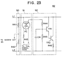
NCU 82 shown in FIG.19. ThisNCU 82 includes aring detection circuit 90, a dialingcircuit 91 and a DC loop (or pseudo inductance)circuit 92. Thering detection circuit 90 is made up of voltage dividing resistors R41 and R42. The dialingcircuit 91 is made up of a photocoupler PC and a resistor R43. This dialingcircuit 91 outputs a dial signal to the wires L1 and L2 of the telephone line based on a signal from a dial signal generator (not shown). TheDC loop circuit 92 includes voltage dividing resistors R44 and R45, a capacitor C41 for bypassing the AC signal, transistors TR1 and TR2 for forming a DC loop, and an emitter resistance R46 of the transistor TR2. - Accordingly, the
ring detection circuit 90 divides the voltage on the telephone line by the voltage dividing resistors R41 and R42. This divided voltage is input to themodem circuit 85 shown in FIG.19 wherein the call and the off-hook is detected. The dialingcircuit 91 inputs the signal from the dialing signal generator and outputs a dial signal to the wires L1 and L2 of the telephone line via the photocoupler PC. TheDC loop circuit 92 divides the DC voltage on the telephone line by the voltage dividing resistors R44 and R45, and this divided voltage is applied to the base of the transistor TR1 as the bias voltage of the transistors TR1 and TR2. As a result, an approximately instant DC current flows to the telephone line via the transistors TR1 and TR2. - FIG.24 shows an embodiment of the
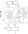
hybrid circuit 84 shown in FIG.19. In FIG.24, those parts which are basically the same as those corresponding parts in FIG.4 are designated by the same reference numerals, and a description thereof will be omitted. - The
hybrid circuit 84 shown in FIG.24 includes a send signal cut off circuit 5, anddifferential circuits differential circuit 6. Thehybrid circuit 84 is coupled to theNCU 82 via the capacitors C1 and C2. Thehybrid circuit 84 inputs the balanced signals from the telephone line and outputs unbalanced signals to themodem circuit 85. In addition, thehybrid circuit 84 inputs unbalanced signals from themodem circuit 85 and outputs balanced signals to the telephone line. - When receiving the signal from the telephone line, the AC signal component of the received signal which is received from the telephone line via the
NCU 82 is input to thedifferential circuit 6. The received signal is essentially made up of balanced signals. The signal from the capacitor C1 is input to thenon-inverting input terminal 10 of thedifferential circuit 6. The signal from the capacitor C2 is input to the inverting input terminal 11 of thedifferential circuit 6. The polarity of the signal input to the inverting input terminal 11 is inverted by taking the input signal from thenon-inverting input terminal 10 as a reference voltage, and is output from the receivedsignal output terminal 14. Accordingly, the input balanced signals are output from thedifferential circuit 6 as unbalanced signals. - On the other hand, when transmitting the signal to the telephone line, the send signal (unbalanced signals) which is converted into the analog form in the
modem circuit 85 is input to the sendsignal input terminal 15 of theoperational amplifier 17 within thedifferential circuit 7, and the polarity of the send signal is inverted before being output from the invertedsignal output terminal 12. In addition, the output of theoperational amplifier 17 is input to the inverting input terminal of theoperational amplifier 18, and the polarity of this output is inverted before being output from thenon-inverting output terminal 13. The signal is output from thenon-inverting output terminal 13 with the same phase as the signal input to the sendsignal input terminal 15. The outputs of theoperational amplifiers NCU 82. - FIG.25 shows an essential part of a fifth embodiment of the modem unit according to the present invention. In FIG.25, those parts which are the same as those corresponding parts in FIG.19 are designated by the same reference numerals, and a description thereof will be omitted.
- In this embodiment, a modem IC card 71A is provided with a
switch 95 which switches the connection between a case where the input signal of the modem IC card 71A is input to the NCU 82 (that is, to connect to the telephone line) and a case where the input signal of the modem IC card 71A is input to the modem circuit 85 (that is, to connect to the mobile telephone 72). - When making the data communication via the
mobile telephone 72, the connectingcable 74 connects the modem IC card 71A and themobile telephone 72, and the connection of theswitch 95 is switched so as to connect the terminals A and B of theconnector 73 to themodem circuit 85. On the other hand, when making the data communication via thetelephone line 255, a connecting cable such as the connectingcable 74A shown in FIG.21 is used to connect the modem IC card 71A to thetelephone line 255. In this case, the connection of theswitch 95 is switched so as to connect the terminals A and B of theconnector 73 to theNCU 82. - FIG.26 shows an embodiment of the connecting cable which is used to connect the modem IC card 71A to the
telephone line 255. In FIG.26, those parts which are the same as those corresponding parts in FIG.21 are designated by the same reference numerals, and a description thereof will be omitted. In FIG.26, aconnector 73A'' has four terminals A, B, C and D corresponding to the terminals A, B, C and D of theconnector 73 of the modem IC card 71A. - According to the fourth and fifth embodiments, it is possible to easily make a data communication using the personal computer and the mobile telephone, even at a location where no telephone line is available. In addition, the connection of the modem IC card to the mobile telephone or to the telephone line can be easily achieved by changing the connecting cable. Further, it is also possible to provide a switch in the modem IC card so that the same connecting cable may be used to connect the modem IC card to the mobile telephone or to the telephone line by merely switching the connection of the switch. Moreover, the connections of the modem IC card to the mobile telephone and the telephone line can both be realized using a connector having a small number of terminals.
- There are modem units which can be connected to an external unit having functions different from the original functions of the modem unit. But the modem unit must form a DC loop circuit with the telephone line in the off-hook state, so that the off-hook of the terminal equipment can be detected at the central office from the current change caused by the off-hook. The DC current which flows to this DC loop circuit must be in the range of 20 to 120 mA according to the standard, for example. Hence, it is necessary to conform to this standard also when the external unit is connected to the modem unit.
- FIG.27 shows a conceivable modem unit which is connectable to an external or option unit. In FIG.27, those parts which are the same as those corresponding parts in FIG.18 are designated by the same reference numerals, and a description thereof will be omitted.
- In FIG.27, the
connector 280 is integrally formed on themodem unit 260. A connector 280' is connected to a connecting cable of areceptacle 285 which connects to the telephone line, and is connectable to theconnector 280 of themodem unit 260. Thereceptacle 285 connects to a connector (not shown) of the telephone line. Aconnector 282 is integrally formed on themodem unit 260. A connector 282' is connected to an end of a connecting cable of an external oroption unit 286, and is connectable to theconnector 282 of themodem unit 260. - For example, the
option unit 286 uses the power which is supplied from the telephone line and functions as an external power unit of themodem unit 260. In this case, the connector 282' of theoption unit 286 is connected to theconnector 282 of themodem unit 260, so as to connect theoption unit 286 and themodem unit 260. But in this conceivable arrangement, theoption unit 286 is connected in parallel to the DC loop circuit. For this reason, the impedance with respect to the telephone line becomes small, thereby making it impossible to conform to the standard described above. - Next, a description will be given of sixth through twelfth embodiments of the modem unit according to the present invention, in which the current value standard with respect to the telephone line can be satisfied even when the option unit is connected to the modem unit. In the sixth through twelfth embodiments, the DC loop circuit of the modem unit is disconnected from the telephone line when the option unit is connected to the modem unit, so that a resistance approximately the same as that of the DC loop circuit is achieved by an internal circuit of the option circuit. If the internal impedance of the option unit is relatively high, the DC loop circuit may remain connected to the telephone line.
- First, a description will be given of the sixth embodiment, by referring to FIG.28. In FIG.28, those parts which are the same as those corresponding parts in FIG.27 are designated by the same reference numerals, and a description thereof will be omitted.
- In FIG.28 (A), only an essential part of a
modem unit 301 is shown. Themodem unit 301 integrally comprises aconnector 280 and aconnector 307. The connector 280' is connected to the telephone line via thereceptacle 285. When the connector 280' is connected to theconnector 280 of themodem unit 301, terminals A and B of the connector 280' respectively connect to terminals A and B of theconnector 280. The terminals A and B of theconnector 280 are respectively connected to wires L1 and L2 which connect to theDC loop circuit 133. - On the other hand, the
connector 307 of themodem unit 301 includes a terminal C which is connected to the wire L1, a terminal D which is connected directly to theDC loop circuit 133, and a terminal E which is connected to the wire L2. A connector 307' is connected to theconnector 307 of themodem unit 301 when connecting theoption unit 309 to themodem unit 301. Terminals C and E of the connector 307' are connected to aninternal circuit 309a of theoption unit 309. Thisinternal circuit 309a has an impedance which is approximately the same as that of theDC loop circuit 133. The terminals C, D and E of the connector 307' respectively connect to the terminals C, D and E of theconnector 307 of themodem unit 301 when theconnectors 307' and 307 are connected to each other. - FIG.28 (B) shows a connector 307'' which is connected to the
connector 307 of themodem unit 301 when no option unit is connected to themodem unit 301. This connector 307'' also has terminals C, D and E, however, the terminals D and E are short-circuited by a short-circuit line SCL. - When connecting the
modem unit 301 to the telephone line, the connector 280' is connected to theconnector 280 of themodem unit 301. In addition, when connecting theoption unit 309 to themodem unit 301, the connector 307' is connected to theconnector 307 of themodem unit 301. As a result, a loop is formed. This loop starts from the telephone line and ends at the telephone line via the terminal A of the connector 280', the terminal A of theconnector 280, the terminal C of theconnector 307, the terminal C of the connector 307', theinternal circuit 309a of theoption unit 309, the terminal E of the connector 307', the terminal E of theconnector 307, the terminal B of theconnector 280 and the terminal B of the connector 280'. On the other hand, theDC loop circuit 133 is disconnected from the telephone line. - Accordingly, by setting the impedance of the
internal circuit 309a of theoption unit 309 so as to conform to the standard of the telephone line, it is possible to make the current flowing through the telephone line to conform to the standard even when theoption unit 309 is connected to themodem unit 301. - In addition, when no option unit is connected to the
modem unit 301, the connector 307'' shown in FIG.28 (B) is connected to theconnector 307 of themodem unit 301. As a result, a loop is formed. This loop starts from the telephone line and ends at the telephone line via the terminal A of the connector 280', the terminal A of theconnector 280, theDC loop circuit 133, the terminal D of theconnector 307, the terminal D of the connector 307'', the short-circuit line SCL, the terminal E of the connector 307'', the terminal E of theconnector 307, the terminal B of theconnector 280 and the terminal B of the connector 280'. Therefore, a current conforming to the standard flows through the telephone line. - Next, a description will be given of the operating principle of the seventh embodiment, by referring to FIG.29. In FIG.29, those parts which are the same as those corresponding parts in FIG.28 are designated by the same reference numerals, and a description thereof will be omitted.
- When connecting the
option unit 309 to themodem unit 301, aconnector 280A is connected to theconnector 280 of themodem unit 301 as shown in FIG.29 (A). As a result, the terminals A and B of theconnector 280A are respectively connected to the terminals A and B of theconnector 280, thereby connecting themodem unit 301 to the telephone line via thereceptacle 285. In addition, terminals C, D and E of theconnector 280A are respectively connected to the terminals C, D and E of theconnector 280, thereby connecting themodem unit 301 to theoption unit 309. Hence, similarly to the sixth embodiment shown in FIG.28, the DC loop of the telephone line is formed via the internal circuit of theoption unit 309, and theDC loop circuit 133 is disconnected from the telephone line. For this reason, it is possible to flow through the telephone line a current which conforms to the standard by appropriately setting the impedance of the internal circuit within theoption unit 309. - On the other hand, when connecting no option unit to the
modem unit 301, aconnector 280B is connected to theconnector 280 of themodem unit 301 as shown in FIG.29 (B). In this case, since the short-circuit line SCL short-circuits the terminals D and E of theconnector 280B, theDC loop circuit 133 is connected to the telephone line and it is possible to flow through the telephone line a current which conforms to the standard. - FIG.30 shows the seventh embodiment in more detail. In FIG.30, those parts which are the same as those corresponding parts in FIGS.27 and 29 are designated by the same reference numerals, and a description thereof will be omitted.
- In FIG.30, (A) shows the case where no option unit is connected to the
modem unit 301, and (B) shows the case where theoption unit 309 is connected to themodem unit 301. - In FIG.30 (A), the
connector 280B is connected to theconnector 280 of themodem unit 301 when connecting the telephone line to themodem unit 301 but no option unit. Theconnector 280B includes terminals which are connected to the telephone line via thereceptacle 285, and terminals which are short-circuited by the short-circuit line SCL. Hence, when theconnector 280B is connected to theconnector 280, themodem unit 301 is automatically connected to the telephone line and the loop is formed via the short-circuit line SCL similarly as described above with reference to FIG.28 (B). - In FIG.30 (B), the
connector 280A is connected to theconnector 280 of themodem unit 301 when connecting themodem unit 301 to the telephone line and to theoption unit 309. Theconnector 280A includes terminals which are connected to the telephone line via thereceptacle 285, and terminals which are connected to theoption unit 309. In this case, the loop is formed via the internal circuit of theoption unit 309, similarly as described above with reference to FIG.28 (A). - Next, a description will be given of an eighth embodiment of the modem unit according to the present invention, by referring to FIG.31. In FIG.31, those parts which are the same as those corresponding parts in FIG.28 are designated by the same reference numerals, and a description thereof will be omitted. In this embodiment, it is assumed that the internal circuit of the
option unit 309 has a high impedance. - In FIG.31, a
connector 280C is connected to theconnector 280 of themodem unit 301. Terminals A and B of theconnector 280C respectively connect to the terminals A and B of theconnector 280, and terminals C, D and E of theconnector 280C respectively connect to the terminals C, D and E of theconnector 280. As a result, themodem unit 301 is connected to the telephone line via the terminals A and B and thereceptacle 285. In addition, themodem unit 301 is connected to theoption unit 309 via the terminals C, D and E. Because the terminals D and E of theconnector 280C are short-circuited, both theoption unit 309 and theDC loop circuit 133 are connected in parallel to the telephone line. However, the internal circuit of theoption unit 309 has a high impedance. Therefore, the current flowing through the telephone line is determined by theDC loop circuit 133 and conforms to the standard. - If no option unit needs to be connected to the
modem unit 301, theconnector 280B shown in FIG.29 (B) is connected to theconnector 280 in place of theconnector 280C. - Next, a description will be given of a ninth embodiment of the modem unit according to the present invention, by referring to FIG.32. In FIG.32, those parts which are the same as those corresponding parts in FIG.28 are designated by the same reference numerals, and a description thereof will be omitted. In this embodiment, the connecting cable of the receptacle is drawn out via the option unit.
- In FIG.32, a
connector 280D is connected to theconnector 280 of themodem unit 301. Terminals A and B of theconnector 280D respectively connect to the terminals A and B of theconnector 280, and terminals C, D and E of theconnector 280C respectively connect to the terminals C, D and E of theconnector 280. As a result, themodem unit 301 is connected to the telephone line via the terminals A and B, theoption unit 309 and thereceptacle 285. In other words, thereceptacle 285 is connected to theoption unit 309. In addition, themodem unit 301 is connected to theoption unit 309 via the terminals C, D and E. In this embodiment, the signal at the terminal A is the same as the signal at the terminal C, and thus, it is possible to use a single terminal in common as the terminals A and C. The current flowing through the telephone line is also determined by theDC loop circuit 133 and conforms to the standard, similarly to the above described embodiment. - If no option unit needs to be connected to the
modem unit 301, theconnector 280B shown in FIG.29 (B) is connected to theconnector 280 in place of theconnector 280D. - Next, a description will be given of a tenth embodiment of the modem unit according to the present invention, by referring to FIG.33. In FIG.33, those parts which are the same as those corresponding parts in FIGS.23 and 28 are designated the same reference numerals, and a description thereof will be omitted.
- In this embodiment, the pseudo inductance circuit (or DC loop circuit) 92 is made up of active elements, and the input side of the
pseudo inductance circuit 92 is connected to theconnector 280. - If no option unit is to be connected to the
modem unit 301, the terminals C and D of theconnector 280 are short-circuited. Hence, the DC voltage on the telephone line is divided by the resistors R44 and R45 and applied to the transistors TR1 and TR2 as the bias voltage. As a result, an approximately constant current flows in a loop circuit which starts from the telephone line and ends at the telephone line via the diode D1 of thediode bridge 22, the transistor TR1, the transistor TR2, the resistor R46 and the diode D4 of thediode bridge 22 or, via the diode D2 of thediode bridge 22, the transistor TR1, the transistor TR2, the resistor R46 and the diode D3 of thediode bridge 22. - On the other hand, when connecting the option unit to the
modem unit 301, the terminals C and E of theconnector 280 are connected to the option unit and the terminals C and D of theconnector 280 are open-circuited. Of course, the terminals C and D of theconnector 280 may be short-circuited if the internal circuit of the option unit has a high impedance. As a result, no current flows to the resistors R44 and R45, and the base voltage of the transistor TR1 becomes equal to the emitter voltage of the transistor TR2, and no current flows to the transistors TR1 and TR2. - Next, a description will be given of an eleventh embodiment of the modem unit according to the present invention, by referring to FIG.34. In FIG.34, those parts which are the same as those corresponding parts in FIG.33 are designated the same reference numerals, and a description thereof will be omitted.
- In this embodiment, the pseudo inductance circuit (or DC loop circuit) 92 is made up of active elements, and the output side of the
pseudo inductance circuit 92 is connected to theconnector 280. - If no option unit is to be connected to the
modem unit 301, the terminals C and D of theconnector 280 are short-circuited. Hence, thepseudo inductance circuit 92 operates similarly to the tenth embodiment. - On the other hand, when connecting the option unit to the
modem unit 301, the terminals C and E of theconnector 280 are connected to the option unit and the terminals C and D of theconnector 280 are open-circuited. Of course, the terminals C and D of theconnector 280 may be short-circuited if the internal circuit of the option unit has a high impedance. As a result, the outputs of the transistors TR1 and TR2 are disconnected from the telephone line, and the telephone line and the option unit are connected. By setting the resistances of the resistors R44 and R45 to sufficiently high resistances, the current flowing through these resistors R44 and R45 becomes negligible. - Next, a description will be given of a twelfth embodiment of the modem unit according to the present invention, by referring to FIG.35. In FIG.35, those parts which are the same as those corresponding parts in FIGS.19, 24 and 28 are designated by the same reference numerals, and a description thereof will be omitted.
- In FIG.35, the terminals A and B of the
connector 280 of themodem unit 301 are respectively connected to the telephone line. When connecting no option unit, the terminals D and E of theconnector 280 are short-circuited, and the telephone line is connected to thepseudo inductance circuit 83. On the other hand, when connecting the option unit to themodem unit 301, the terminals C and E of theconnector 280 are connected to the option unit, and the terminals D and E are open-circuited . Alternatively, if the internal circuit of the option unit has a high impedance, the terminals D and E of theconnector 280 may be short-circuited. - The operation of the
modem unit 301 at the time of the signal reception and signal transmission is basically the same as that described above. - Therefore, according to the sixth through twelfth embodiments, it is possible to automatically control the current flowing through the telephone line so as to conform to the standard when the off-hook is detected, even if the option unit is connected to the modem unit. In addition, the flexibility of the modem unit is greatly improved particularly when the entire modem unit is made in the form of the IC, that is, the modem IC card.
- The advantages of the modem IC card having the entire modem unit made in the form of the IC have been described above. But when using the modem IC card with a portable data processing unit, for example, it is important that the power consumption of the modem IC card is small particularly when the modem IC card is battery-operated. In other words, it is desirable that the power consumption of the modem IC card is small so that the modem IC card can be used for a long time without the need to replace or charge the battery thereof.
- Next, a description will be given of the problems of the conventional battery-operated modem unit, by referring to FIG.36.
- In FIG.36, a
modem unit 480 is connected between the telephone line and aterminal equipment 481 such as a portable personal computer. Themodem unit 480 modulates send data which is output from theterminal equipment 481 into an analog signal, and transmits the analog signal to a remote end via the telephone line. In addition, themodem unit 480 demodulates analog received data which is received from the remote end via the telephone line into digital data, and supplies the digital data to theterminal equipment 481. - The
modem unit 480 includes anoscillator 482, apower unit 483 which is a battery in this case, and amodem processor 484. Themodem processor 484 is made up of amodem controller 485 and a modem circuit 486. - The
oscillator 482 generates clock pulses for driving themodem processor 484. Thepower unit 483 supplies the driving power to themodem processor 484. Themodem processor 484 modulates the send data and demodulates the received data in response to the clock pulses generated from theoscillator 482. - The
modem controller 485 controls the input and output of the send data and the received data, and also controls the modulation and demodulation. Themodem controller 485 includes a clock pulse input terminal CLK for receiving the clock pulses, a power source voltage input terminal Vcc for receiving the power source voltage, an input terminal SD for receiving the send data from theterminal equipment 481, and an output terminal RD for outputting the demodulated received data. - The modem circuit 486 includes a modem and a processor. The modem modulates the send data in response to the clock pulses, and also demodulates the received data in response to the clock pulses. On the other hand, the processor carries out a predetermined processing on the data such as error correction, data compression and data expansion depending on the communication mode which is determined by the communication between the
terminal equipment 481 and the terminal equipment (not shown) on the remote end. - However, the frequency of the clock pulses generated from the
oscillator 482 was conventionally fixed. Hence, it is possible to reduce the power consumption of themodem unit 480 by decreasing the frequency, but the processing speed of themodem unit 480 will deteriorate in this case. For this reason, the frequency of the clock pulses is set to a frequency which is as high as possible. - It is conceivable to obtain the power for the
modem unit 480 from the telephone line. However, the power which can be obtained from the telephone line is small, and an LSI which can operate at such a small power only has a communication speed of approximately 1200 bps at the maximum. But the recent modem unit generally operates at the communication speed of 2400 bps and require functions such as self-error correction, data compression/expansion, it is virtually impossible to satisfactorily drive such a modem unit by the power obtained from the telephone line. - On the other hand, it is also conceivable to have the terminal equipment carry out the functions such as self-error correction and data compression/expansion, but this would only shorten the life of the battery which drives the terminal equipment.
- Next, a description will be given of the operating principle of thirteenth and fourteenth embodiments of the modem unit according to the present invention, by referring to FIG.37. In these embodiments, the modem unit is normally driven by high-frequency clock pulses when the power source voltage of the modem unit is sufficiently high. But if the power source voltage decreases, the frequency of the clock pulses is decreased automatically so as to operate at a lower power consumption. It is also possible to simplify the processes by eliminating the error correction function, for example. The modem unit on the remote end is notified of the mode of the modem unit, so that the communication can be made according to the mode.
- In FIG.37, a
modem unit 501 has the form of the modem IC card and is loaded into aterminal equipment 506 which may be a portable personal computer. Of course, themodem unit 501 in principle may be connected externally to theterminal equipment 506. - The
modem unit 501 generally includes abattery 515, a power sourcevoltage detection circuit 502, avoltage holding circuit 503, aclock generator 504, and amodem processor 507. - The
battery 515 may be built into themodem unit 501 or may be the power unit of theterminal equipment 506 in the case where themodem unit 501 is loaded into theterminal equipment 506. For the sake of convenience, it will be assumed that thebattery 515 is built into themodem unit 501. - The
voltage detection circuit 502 detects the voltage state of thebattery 515. Thevoltage holding circuit 503 holds a voltage state value indicative of the voltage level detected by thevoltage detection circuit 502. Theclock generator 504 generates clocks having different frequencies. Theclock generator 504 includes aclock frequency selector 505 which selects the clock frequency at which themodem unit 501 to operate. Themodem processor 507 carries out processings such as error correction, data compression and data expansion in addition to modulating the send data and demodulating the received data. - The
modem processor 507 includes amodem controller 516, afunction processor 511 and amodem 509. Themodem controller 516 includes a modemfunction determination circuit 508 and a message send circuit 514, and carries out the control functions of themodem unit 501. the modemfunction determination circuit 508 determines the function to be processed by themodem unit 501. Thefunction processor 511 includes anerror correction circuit 512 and a data compression/expansion circuit 513, and carries out functions other than modulation and demodulation, such as error correction and data compression/expansion. Theerror correction circuit 512 corrects the error in the data, and the data compression/expansion circuit 513 compresses and expands the data. Themodem 509 includes aswitching circuit 510 which switches the communication path to the remote end from theterminal equipment 506 to the modemfunction determination circuit 506 when notifying the mode of themodem unit 501 to the terminal equipment on the remote end. This mode indicates the selected functions such as the communication speed and error correction. - The
voltage detection circuit 502 constantly monitors the voltage from thebattery 515, and outputs a voltage state value indicative of the detected voltage level. Thevoltage holding circuit 503 holds this voltage state value. Theclock generator 504 selects the clock frequency which is used to drive themodem unit 501 depending on the voltage state value held in thevoltage holding circuit 503. If the voltage level of thebattery 515 is sufficiently high, theclock generator 504 selects a high clock frequency. On the other hand, theclock generator 504 selects a low clock frequency if the voltage level of thebattery 515 is low. Themodem processor 507 operates responsive to the clock pulses having the clock frequency which is selected by theclock frequency selector 505 of theclock generator 504. - The modem
function determination circuit 508 selects the required function or functions depending on the voltage state value and the function request information from theterminal equipment 506. For example, if the voltage level of thebattery 515 is sufficiently high, it is possible to satisfy all of the required functions requested from theterminal equipment 506, and these functions are selected. On the other hand, if the voltage level of thebattery 515 is low, the processing in themodem processor 509 is simplified so that a high-speed process can be carried out even in response to the low-clock frequency. In other words, if theterminal equipment 506 requests the error correction and the data compression/expansion, the modemfunction determination circuit 508 determines whether to carry out only the error correction, to carry out only the data compression/expansion or not to carry out the error correction and the data compression/expansion, for example. If one of the error correction and the data compression/expansion is to be selected, the error correction is selected with a priority over the data compression/expansion. - Prior to starting the communication, the modem
function determination circuit 508 notifies the remote end of the determined processing function via theswitching circuit 510 and the telephone line, so as to set the communication mode. In addition, the modemfunction determination circuit 508 also notifies theterminal equipment 506 of the set mode. Theterminal equipment 506 makes the data communication with the terminal equipment on the remote end in accordance with the mode which is set by themodem unit 501. - The
function processor 511 inputs the function request information from the remote end via theswitching circuit 510, and determines the function. In addition, based on the function request information from theterminal equipment 506, thefunction processor 511 supplies the processable function which is determined by themodem unit 501 depending on the voltage state value to theterminal equipment 506 via the message sending circuit 514. - If a low function request is made from the
terminal equipment 506 when the voltage level of thebattery 515 is sufficiently high, that is, if the instruction from theterminal equipment 506 indicates that no error correction and no data compression/expansion are required, for example, the communication can be made at a sufficiently high speed even in response to low-frequency clock pulses. Hence, in this case, the modemfunction determination circuit 508 instructs theclock frequency selector 505 to select the low clock frequency, so as to extend the serviceable life of thebattery 515. - The modulation and demodulation operations of the
modem 509 are the same as those of the conventional modem unit. In addition, the operations of the data compression/expansion circuit 513 and theerror correction circuit 512 are the same as those of the conventional modem unit, except that the processing of the data compression/expansion circuit 513 and theerror correction circuit 512 is started in response to the instruction from thefunction determination circuit 508. - According to these embodiments, the
modem unit 501 can operate even when the voltage level of thebattery 515 decreases. In addition, the deterioration in the processing quantity caused by the decreased clock pulse frequency is compensated for by reducing the functions to be carried out, so as to enable a highspeed communication even where the clock pulse frequency is low. Furthermore, since the function selection can be made in steps, it is possible to carry out as much functions as possible depending on the voltage level of thebattery 515. - Moreover, if the
terminal equipment 506 does not request high functions in a state where the voltage level of thebattery 515 is high, it is possible to select the low clock pulse frequency so as to prevent unnecessary wear of thebattery 515. - Of course, it is possible to operate only the
modem controller 516 in response to the clock pulses which are selected by theclock frequency selector 505, and operate themodem 509 in response to basic clock pulses. - Next, a more detailed description will be given of the thirteenth embodiment, by referring to FIG.38. In FIG.38, a
modem unit 520 and aterminal equipment 530 respectively correspond to themodem unit 501 and theterminal equipment 506 shown in FIG.37. In addition, abattery 521, avoltage detection circuit 522, a voltage statevalue holding circuit 524, aclock generator 525 and amodem processor 527 shown in FIG.38 respectively correspond to thebattery 515, thevoltage detection circuit 502, the voltage statevalue holding circuit 503, theclock generator 504 and themodem processor 507 shown in FIG.37. In this embodiment, amodem controller 528 of themodem processor 527 is driven by clock pulses which are selected depending on the voltage level of thebattery 521. In addition, amodem 529 of themodem processor 527 is driven by basic clock pulses. Thismodem 529 is provided on an LSI which is independent of an LSI on which the remaining parts of themodem unit 520 are provided. - The
voltage detection circuit 522 includesvoltage comparators 523, 523' and 523''. Thevoltage comparator 523 compares the power source voltage from thebattery 521 and a threshold value TH1, so as to detect the state of the power source voltage. For example, thevoltage comparator 523 outputs a signal "1" if the power source voltage is higher than the threshold value TH1 and outputs a signal "0" if lower. Similarly, the voltage comparator 523' compares the power source voltage and a threshold value TH2, so as to detect the state of the power source voltage. The voltage comparator 523'' compares the power source voltage and a threshold value TH3, so as to detect the state of the power source voltage. - The
voltage holding circuit 524 holds the state of the power source voltage as the voltage state value depending on the outputs of thevoltage comparators 523, 523' and 523''. For example, if the threshold values are such that TH1 > TH2 > TH3, the voltage state value is set to "011" when the power source voltage is lower than TH1 and higher than TH2. In this case, the state of the power source voltage can be held as a voltage state value having three stages. - A reset signal *RST is supplied to the voltage state
value holding circuit 524 and to themodem controller 528. - The
clock generator 525 includes an oscillator 525' and afrequency divider 526. The oscillator 525' generates basic clock pulses having a maximum clock pulse frequency of 30 MHz, for example. Thefrequency divider 526 frequency-divides the frequency of the basic clock pulses output from the oscillator 525' depending on the voltage state value which is held by the voltage statevalue holding circuit 524. For example, thefrequency divider 526 generates clock pulses having clock frequencies of 30/n MHz, where n denotes the frequency dividing ratio. - The
modem processor 527 includes themodem controller 528, themodem 529 and a function processor 529'. - The
frequency divider 526 determines the frequency dividing ratio of the basic clock pulses depending on the voltage state value which is held in the voltagestate holding circuit 524, and outputs the clock pulses having the frequency-divided frequency. For example, if the voltage level of thebattery 521 is sufficiently high, the voltage state value is large, and the basic clock pulses having the frequency of 30 MHz is selectively output from thefrequency divider 526 in this case. But if the voltage level of thebattery 521 decreases, the voltage state value decreases, and the clock pulses having the frequency of 20 MHz is output from thefrequency divider 526. Hence, the clock pulses having the maximum operable frequency is selected and output from thefrequency divider 526 depending on the voltage level of thebattery 521, that is, the power source voltage level. - The voltage state value from the voltage state
value holding circuit 524 is input to the input port of themodem controller 528. Themodem controller 58 compares this voltage state mode and the function request from theterminal equipment 530, and sets the most appropriate operation mode, that is, the mode in which the most appropriate function process is selected. - The
modem controller 528 and the function processor 529' operate responsive to the clock pulses determined by thefrequency divider 526. On the other hand, themodem 529 operates responsive to the basic clock pulses which have the frequency of 30 MHz and are output from the oscillator 525'. - Next, a description will be given of an embodiment of the
modem processor 527, by referring to FIG.39. In FIG.39, those parts which are the same as those corresponding parts in FIG.38 are designated by the same reference numerals, and a description thereof will be omitted. - The
modem controller 528 includesregisters register comparator 542, aregister 543, afunction determination circuit 544, acommand analyzer 545 and amessage sending circuit 546. Themodem 529 includes aswitching circuit 547. The function processor 529' includes anerror correction circuit 548 and a data compression/expansion circuit 549. - In the
modem controller 528, theregister 540 stores the function request information which is received from theterminal equipment 530 via thecommand analyzer 545. Theregister 541 stores the voltage state value input from the voltage statevalue holding circuit 524. Theregister comparator 542 compares the contents of theregisters register 543 stores the comparison result output from theregister comparator 542. - The
function determination circuit 544 determines the function which is to be processed in themodem unit 520 depending on the content of theregister 543. Theerror correction circuit 548 and the data compression/expansion circuit 549 are turned ON/OFF, that is, controlled to active/inactive state, depending on the determination result of thefunction determination circuit 544. Thecommand analyzer 545 analyzes the function request information from theterminal equipment 530. In addition, when thecommand analyzer 545 receives from the terminal equipment 530 a query command of the function process which is determined by thefunction determination circuit 544, thecommand analyzer 545 controls the message sendcircuit 546 to transfer a message related to this function. - The message send
circuit 546 stores the information read out from theregister 543 and send this information to theterminal equipment 530 depending on the function to be processed which is determined by thefunction determination circuit 544 or depending on the function information query command from theterminal equipment 530. - Next, a description will be given of the operation of the system shown in FIG.39. The
frequency divider 526 outputs the clock pulses having the frequency dependent on the voltage state value, and are supplied to themodem controller 528. The voltage state value held in the voltagestate holding circuit 524 is input to theregister 541 via the input port of themodem processor 527. On the other hand, the function request command from theterminal equipment 530 is input to thecommand analyzer 545, and the analyzed command is stored in theregister 540. Theregister comparator 542 compares the values stored in theregisters register 543. - For example, the
register comparator 542 compares the voltage state value and the request value which is determined depending on the request from theterminal equipment 530. This request value has a large value when the function request is large such as the case where both the error correction and data compression/expansion are requested, and is small when the function request is small such as the case where there is no function request and both the error correction and data compression/expansion are unnecessary. Theregister comparator 542 selects the larger value and stores this value into theregister 543. - The
function determination circuit 544 determines the function to be processed depending on the value stored in theregister 543, and selects the function of the function processor 529'. If the error correction is required, thefunction determination circuit 544 turns ON a start signal which is supplied to theerror correction circuit 548, and thefunction determination circuit 544 otherwise turns this start signal OFF. In addition if the data compression/expansion is required, thefunction determination circuit 544 turns ON a start signal which is supplied to the data compression/expansion circuit 549, and thefunction determination circuit 544 otherwise turns this start signal OFF. - Prior to making the data communication, it is necessary to notify the terminal equipment on the remote end the functions of the
terminal equipment 530. Hence, theswitching circuit 547 switches the communication path from the path to the telephone line to the path from theterminal equipment 530 to thefunction determination circuit 544. The function determined by thefunction determination circuit 544 is notified to the remote end, and the remote end carries out a control so as to make the processing by the same function. Such a control may be realized according to the CCITT Recommendations V.42/42bis. Thefunction determination circuit 544 notifies theterminal equipment 530 of the function which is determined as a result of the communication with the remote end, as an indication message. - The
function determination circuit 544 also inputs the function request information from the remote end via theswitching circuit 547, and determines the function. - In this state, the
terminal equipment 530 cannot confirm whether the message which is received as the indication message is caused by the active selection of themodem unit 520 or by an erroneous operation. Hence, thefunction determination circuit 544 sends to the message send circuit 546 a function selection message which indicates that the indication message is caused by the active selection of thefunction determination circuit 544. Themessage end circuit 546 sends this function selection message to theterminal equipment 530. - When the
command analyzer 545 receives from the terminal equipment 530 a query command of a function which can be processed by themodem unit 520, thecommand analyzer 545 reads the value stored in theregister 543 into the message sendcircuit 546. The message sendcircuit 546 then sends the content of theregister 543 to theterminal equipment 530. - Next, a more detailed description will be given of the fourteenth embodiment, by referring to FIGS.40 and 41. FIG.40 shows the fourteenth embodiment, and FIG.41 shows an embodiment of the
modem controller 528 shown in FIG.40. In FIGS.40 and 41, those parts which are the same as those corresponding parts in FIGS.38 and 39 are designated by the same reference numerals, and a description thereof will be omitted. - In this embodiment, a determination result which is related to the function to be processed and is made in the
function determination circuit 544 of themodem controller 528 is reflected to the selection of the frequency dividing ratio in thefrequency divider 526. In other words, the voltage statevalue holding circuit 524 includes a voltage state value selection circuit 524' which selects a voltage state value corresponding to the determination result made in thefunction determination circuit 544. The selected voltage state value is supplied to thefrequency divider 526. - If the power source voltage is high and the voltage state value is large, the content of the
register 543 is reflected to the selection of the frequency dividing ratio of thefrequency divider 526 when the request value from theterminal equipment 530 is small. - In other words, the voltage state value selection circuit 524' compares the value of the
register 543 referred to by thefunction determination circuit 544 and the value which is input to the voltage statevalue holding circuit 524 from thevoltage detection circuit 522. If the value of theregister 543 is smaller than the voltage state value detected by thevoltage detection circuit 522, the content of theregister 543 is selected and output from thefrequency divider 526. Thefrequency divider 526 outputs clock pulses having a low frequency depending on the function which is determined by thefunction determination circuit 544. As a result, if the power source voltage is sufficiently high and the function request from theterminal equipment 530 is small, the clock pulse frequency is kept low so as to prevent unnecessary wear of thebattery 521. Otherwise, the operation of this embodiment is basically the same as that of the fourteenth embodiment. - Therefore, according to the thirteenth and fourteenth embodiments, the communication will not be disabled immediately when the power source voltage of the modem unit decreases. Instead, the functions of the modem unit are automatically adjusted so that the communication can be continued with the reduced power source voltage, and the communication can be made at a low power consumption. Accordingly, the modem unit can be used for a longer period of time after the power source voltage begins to decrease.
- Further, the present invention is not limited to these embodiments, but various variations and modifications may be made without departing from the scope of the present invention.
Claims (28)
- A modem unit adapted to be coupled between a land or radio telephone line and a terminal equipment, said modem unit comprising modem circuit means (8, 27, 85, 507), coupled to the terminal equipment (250, 251, 506), for modulating data received from the terminal equipment and for demodulating data transmitted to the terminal equipment, characterized in that there is provided: isolation means (C1, C2, 34), coupled to said modem circuit means (8, 27, 85, 507), for providing a DC isolation between the telephone line and the terminal equipment (250, 251, 506), and that said modem circuit means and said isolation means are respectively provided on a single modem integrated circuit card.
- The modem unit as claimed in claim 1, characterized in that all constituent elements of the modem unit are provided on the single modem integrated circuit card.
- The modem unit as claimed in claim 1 or 2, characterized in that said isolation means (C1, C2, 34) includes capacitor means (C1, C2), coupled to the telephone line, for cutting off a DC current from the telephone line and for passing an AC signal from the telephone line, and the modem unit further comprises:
a first differential circuit (6) having a non-inverting input terminal which receives a received signal from one wire of the telephone line via the capacitor means, an inverting input terminal which receives a received signal from the other wire of the telephone line via the capacitor means, and an output terminal which supplies an output analog signal to said modem circuit means characterized in that the analog signal is converted into a digital signal which is transmitted to the terminal equipment; and a second differential circuit (7) having an input terminal which receives a digital signal which originates from the terminal equipment and is converted into an analog input signal in said modem circuit means, and a pair of output terminals which supply an analog signal having a polarity inverted with respect to the analog input signal and an analog signal having the same polarity as the analog input signal to the telephone line via the capacitor means. - The modem unit as claimed in claim 3, characterized in that the first differential circuit (6) inputs balanced signals and outputs unbalanced signals, and the second differential circuit (7) inputs unbalanced signals and outputs balanced signals.
- The modem unit as claimed in claim 3 or 4, characterized in that there are further provided cut off circuit means (5), coupled between the capacitor means (C1, C2) and the first differential circuit (6), for cutting off a signal output from the second differential circuit (7) so that this signal is prevented from being input to the first differential circuit.
- The modem unit as claimed in any of claims 3 to 5, characterized in that the first differential circuit (6) includes an operational amplifier (16), and the second differential circuit (7) includes two operational amplifiers (17, 18) which are coupled in series.
- The modem unit as claimed in any of claims 3 to 6, characterized in that there is further provided pseudo inductance circuit means (2) including a loop circuit for bypassing a DC current from the telephone line, said pseudo inductance circuit means being made up of active elements.
- The modem unit as claimed in claim 1, characterized in that said isolation means (C1, C2, 34) includes photocoupler means (34) for optically exchanging signals between said modem circuit means (8, 27, 85, 507) and the terminal equipment.
- The modem unit as claimed in claim 8, characterized in that there is further provided a power unit (31) for supplying power to various parts of the modem unit, said power unit being isolated from the terminal equipment by the photocoupler means (34).
- The modem unit as claimed in claim 8 or 9, characterized in that there is further provided ring detection circuit means (23), coupled to the telephone line, for detecting a calling signal from a remote end via the telephone line, said ring detection circuit means including voltage dividing resistors (Ra, Rb).
- The modem unit as claimed in any of claims 8 to 10, characterized in that there is further provided polarity detection circuit means (28), coupled to the telephone line, for detecting a polarity inversion of a DC voltage on the telephone line, said polarity detection circuit means including voltage dividing resistors (Rc, Rd).
- The modem unit as claimed in claim 9, characterized in that there are further provided: a DC/DC converter (29), coupled to the telephone line, shifting a DC voltage on the telephone line; and a power switch (32) for selectively outputting one of an output of the DC/DC converter (29) and an output of the power unit (31) as the power which is supplied to the various parts of the modem unit, and that said power switch switches to selectively output the output of the DC/DC converter in response to an off-hook signal.
- The modem unit as claimed in claim 8, characterized in that said isolation means (C1, C2, 34) further includes: pseudo inductance circuit means (25), coupled to the telephone line, for bypassing a DC current from the telephone line, said pseudo inductance circuit means including no transformer; and AC signal transmitting circuit means (26), coupled to the telephone line, for transferring an AC signal from the telephone line to said modem circuit means, said AC signal transmitting circuit means being made up of active elements and including no transformer.
- The modem unit as claimed in claim 1, characterized in that the modem integrated circuit card (66, 66A) has a shape and size which are approximately the same as those of a memory integrated circuit card (54) which is provided with a slot through which a battery of the memory integrated circuit card is replaceable, said modem integrated circuit card (66, 66A) including connecting means (53, 63), provided at a predetermined position corresponding to that of the slot of the memory integrated circuit card (54), for coupling the modem unit to the telephone line.
- The modem unit as claimed in claim 14, characterized in that said connecting means (53, 63) includes a cable (53, 61) which extends outwards from the predetermined position of the modem integrated circuit card (66, 66A).
- The modem unit as claimed in claim 14, characterized in that said connecting means (53, 63) includes a connector (63) which is provided at the predetermined position of the modem integrated circuit card (66, 66A).
- The modem unit as claimed in claim 1, characterized in that there are further provided: network control means (80) having terminals for coupling to the telephone line; and connector means (73, 280) having first terminals (A, B) for coupling to the telephone line, said first terminals being coupled to the terminals of said network control means, said isolation means (C1, C2, 34) including hybrid circuit means (84) for coupling the telephone line and said modem circuit means (85) with respect to an AC signal.
- The modem unit as claimed in claim 17, characterized in that said connector means (73) further includes second terminals (C, D, E) coupled to said modem circuit means (85).
- The modem unit as claimed in claim 17 or 18, characterized in that there is further provided switching means (95), coupled to said connector means (73), for selectively coupling the first terminals (A, B) to one of said network control means (82) and said modem circuit means (85).
- The modem unit as claimed in claim 18 or 19, characterized in that the first terminals (A, B) are connectable to the land telephone line and the second terminals (C, D, E) are connectable to the radio telephone line via a mobile telephone.
- The modem unit as claimed in claim 17, characterized in that said connector means (280) further includes a pair of second terminals (C, E) which are coupled to said hybrid circuit means (84) and a third terminal (D) which is coupled to said network control means (82), said second and third terminals (C, E, D) being connectable to an external unit, one of said second terminals (E) and said third terminal (D) being short-circuited when no external unit is coupled to the modem unit.
- The modem unit as claimed in claim 21, characterized in that the external unit includes an internal circuit which has an internal impedance approximately equal to that of a DC loop formed by the modem unit, said second terminals (E, C) coupling to the internal circuit, said one of the second terminals (E) and the third terminal (D) being open-circuited.
- The modem unit as claimed in claim 17, characterized in that said connector means (280) further includes a pair of second terminals (C, E) which are coupled to said hybrid circuit means (84) and a third terminal (D) which is coupled to said network control means (82), said second and third terminals (C, E, D) being connectable to an external unit, one of said second terminals (E) and said third terminal (D) being short-circuited when said connector means (280) is coupled to the external unit which has a high impedance.
- The modem unit as claimed in claim 1, characterized in that there are further provided: a battery (515) for suppling power to various parts of the modem unit; detection means (502), coupled to said battery, for detecting an output voltage level of said battery; and selection means (504), coupled to said detection means, for selecting a frequency of a clock which drives said modem circuit means depending on the voltage level detected by said detection means, said modem circuit means (507) including determination means (508), coupled to said detection means, for determining a modem function of said modem circuit means based on the voltage level detected by said detection means and function request information specified from the terminal equipment (506).
- The modem unit as claimed in claim 24, characterized in that said modem circuit means (507) includes switching means (510), coupled to said determination means (508), for switching a communication path to the telephone line from the terminal equipment (506) to said determination means so as to notify the modem function determined by said determination means to a terminal equipment on a remote end.
- The modem unit as claimed in claim 24 or 25, characterized in that said modem circuit means (507) includes send circuit means (514), coupled to said detection means (503), for notifying the terminal equipment (506) of a modem function which can be processed depending on the voltage level detected by said detection means (502), said send circuit means notifying the modem function determined by said determination means (508) prior to a start of a data communication or responsive to a request from the terminal equipment.
- The modem unit as claimed in any of claims 24 to 26, characterized in that said selection means (504) inputs function information determined by said determination means (508) and selectively outputs a clock having a frequency lower than normal depending on the modem function if said determination means determines this modem function responsive to a request from the terminal equipment (506).
- The modem unit as claimed in any of claims 24 to 27, characterized in that said modem circuit means (507) comprises: a modem (509) carrying out modulation and demodulation of signals based on a basic clock; a function processor (511), coupled to said modem, carrying out functions other than the modulation and demodulation; and a modem controller (516), coupled to said detection means (502), said selection means (504) and said function processor, controlling said function processor, and that said modem controller (516) operates in response to a clock which is determined based on the voltage level detected by said detection means (502) or the modem function determined by said determination means (508).
Priority Applications (3)
| Application Number | Priority Date | Filing Date | Title |
|---|---|---|---|
| EP95106588A EP0667701A3 (en) | 1992-03-19 | 1993-03-18 | Modem unit |
| EP98116842A EP0886426A3 (en) | 1992-03-19 | 1993-03-18 | Modem unit |
| EP98116841A EP0887990B1 (en) | 1992-03-19 | 1993-03-18 | Modem unit |
Applications Claiming Priority (18)
| Application Number | Priority Date | Filing Date | Title |
|---|---|---|---|
| JP6426692 | 1992-03-19 | ||
| JP6426492 | 1992-03-19 | ||
| JP4064266A JP2881065B2 (en) | 1992-03-19 | 1992-03-19 | Modem device |
| JP6426592A JP2728594B2 (en) | 1992-03-19 | 1992-03-19 | Modem device |
| JP6426592 | 1992-03-19 | ||
| JP64264/92 | 1992-03-19 | ||
| JP6426492A JPH05268379A (en) | 1992-03-19 | 1992-03-19 | Modem |
| JP64266/92 | 1992-03-19 | ||
| JP64265/92 | 1992-03-19 | ||
| JP12511092 | 1992-05-18 | ||
| JP12511092A JPH05327790A (en) | 1992-05-18 | 1992-05-18 | Modem device |
| JP125110/92 | 1992-05-18 | ||
| JP4125111A JPH05327791A (en) | 1992-05-18 | 1992-05-18 | Ic card type modem device and its communication method |
| JP125111/92 | 1992-05-18 | ||
| JP12511192 | 1992-05-18 | ||
| JP4137253A JPH05334505A (en) | 1992-05-28 | 1992-05-28 | I/o card |
| JP13725392 | 1992-05-28 | ||
| JP137253/92 | 1992-05-28 |
Related Child Applications (4)
| Application Number | Title | Priority Date | Filing Date |
|---|---|---|---|
| EP98116841A Division EP0887990B1 (en) | 1992-03-19 | 1993-03-18 | Modem unit |
| EP95106588A Division EP0667701A3 (en) | 1992-03-19 | 1993-03-18 | Modem unit |
| EP98116842A Division EP0886426A3 (en) | 1992-03-19 | 1993-03-18 | Modem unit |
| EP95106588.7 Division-Into | 1993-03-18 |
Publications (3)
| Publication Number | Publication Date |
|---|---|
| EP0561644A2 true EP0561644A2 (en) | 1993-09-22 |
| EP0561644A3 EP0561644A3 (en) | 1995-05-17 |
| EP0561644B1 EP0561644B1 (en) | 2000-01-05 |
Family
ID=27550970
Family Applications (4)
| Application Number | Title | Priority Date | Filing Date |
|---|---|---|---|
| EP98116842A Ceased EP0886426A3 (en) | 1992-03-19 | 1993-03-18 | Modem unit |
| EP98116841A Expired - Lifetime EP0887990B1 (en) | 1992-03-19 | 1993-03-18 | Modem unit |
| EP93302087A Expired - Lifetime EP0561644B1 (en) | 1992-03-19 | 1993-03-18 | Modem unit |
| EP95106588A Withdrawn EP0667701A3 (en) | 1992-03-19 | 1993-03-18 | Modem unit |
Family Applications Before (2)
| Application Number | Title | Priority Date | Filing Date |
|---|---|---|---|
| EP98116842A Ceased EP0886426A3 (en) | 1992-03-19 | 1993-03-18 | Modem unit |
| EP98116841A Expired - Lifetime EP0887990B1 (en) | 1992-03-19 | 1993-03-18 | Modem unit |
Family Applications After (1)
| Application Number | Title | Priority Date | Filing Date |
|---|---|---|---|
| EP95106588A Withdrawn EP0667701A3 (en) | 1992-03-19 | 1993-03-18 | Modem unit |
Country Status (4)
| Country | Link |
|---|---|
| US (1) | US5655009A (en) |
| EP (4) | EP0886426A3 (en) |
| CA (1) | CA2091958C (en) |
| DE (2) | DE69333170T2 (en) |
Cited By (4)
| Publication number | Priority date | Publication date | Assignee | Title |
|---|---|---|---|---|
| GB2289189A (en) * | 1994-05-02 | 1995-11-08 | Motorola Inc | Method for selective connection of a data processor to a telephone line or radio telephone |
| US5699405A (en) * | 1994-04-26 | 1997-12-16 | Nec Corporation | Modem card for portable radiophone |
| US5799069A (en) * | 1994-09-29 | 1998-08-25 | Intel Corporation | Method and apparatus for dynamically adapting the clock rate and data transfer rate of phone-line powered modems. |
| EP1384717A2 (en) * | 1991-11-18 | 2004-01-28 | E.I. Dupont De Nemours And Company | Tetrazolylphenylboronic acid intermediates for the synthesis of A II receptor antagonists |
Families Citing this family (24)
| Publication number | Priority date | Publication date | Assignee | Title |
|---|---|---|---|---|
| US5871429A (en) * | 1994-07-22 | 1999-02-16 | Ranpak Corp. | Cushioning conversion machine including a probe for sensing packaging requirements |
| US6524230B1 (en) * | 1994-07-22 | 2003-02-25 | Ranpak Corp. | Packing material product and method and apparatus for making, monitoring and controlling the same |
| JPH09160848A (en) * | 1995-12-07 | 1997-06-20 | Sony Corp | Transmitter-receiver |
| JP3241597B2 (en) * | 1996-05-24 | 2001-12-25 | 一博 小野 | Personal audio playback device |
| US5896415A (en) * | 1997-05-27 | 1999-04-20 | 3 Com Corporation | Device for out-of-band transmission on computer peripheral |
| US6714590B1 (en) | 1999-07-23 | 2004-03-30 | Silicon Laboratories, Inc. | Integrated modem and line-isolation circuitry and associated method |
| US6724891B1 (en) | 1998-03-04 | 2004-04-20 | Silicon Laboratories Inc. | Integrated modem and line-isolation circuitry and associated method powering caller ID circuitry with power provided across an isolation barrier |
| US6584196B1 (en) * | 1999-05-14 | 2003-06-24 | Conexant Systems, Inc. | Electronic inductor with transmit signal telephone line driver |
| US6662238B1 (en) | 1999-07-23 | 2003-12-09 | Silicon Laboratories Inc. | Integrated modem and line-isolation circuitry with command mode and data mode control and associated method |
| US7020187B1 (en) | 1999-07-23 | 2006-03-28 | Silicon Laboratories Inc. | Integrated modem and line-isolation circuitry with HDLC framing and associated method |
| US6826225B1 (en) | 1999-07-23 | 2004-11-30 | Silicon Laboratories, Inc. | Integrated modem and line-isolation circuitry with selective raw data or modem data communication and associated method |
| US6735246B1 (en) * | 1999-07-23 | 2004-05-11 | Silicon Laboratories Inc. | Integrated modem and line-isolation circuitry with data flow control and associated method |
| US6445791B1 (en) * | 1999-08-09 | 2002-09-03 | Cirrus Logic, Inc. | System and methods for modem interface |
| WO2001046804A1 (en) * | 1999-08-16 | 2001-06-28 | Z-Force Corporation | System of reusable software parts for implementing concurrency and hardware access, and methods of use |
| US6373886B1 (en) * | 2000-01-06 | 2002-04-16 | Pc Tel, Inc. | Power supply circuits for data access arrangement enabling modem operation over a private line |
| FR2826433B1 (en) * | 2001-06-20 | 2003-12-19 | Alstom Power Nv | SECURITY DEVICE FOR INDUSTRIAL BOILER INCLUDING RELAYS MOUNTED ON A PRINTED CIRCUIT BOARD |
| EP1665844A1 (en) * | 2003-09-10 | 2006-06-07 | Siemens Aktiengesellschaft | Extension of the sim card interface in gsm devices |
| US7443911B2 (en) * | 2004-04-07 | 2008-10-28 | Silicon Laboratories Inc. | Communication devices capable of using system clock inputs for embedded television applications |
| KR100648660B1 (en) * | 2004-10-01 | 2006-11-24 | 삼성전자주식회사 | Facsimile's communication interface unit capable of preventing data error caused by noise with using a transformer and the transformer thereof |
| US8948822B2 (en) * | 2008-04-23 | 2015-02-03 | Qualcomm Incorporated | Coordinating power management functions in a multi-media device |
| US8908763B2 (en) * | 2008-06-25 | 2014-12-09 | Qualcomm Incorporated | Fragmented reference in temporal compression for video coding |
| US8964828B2 (en) | 2008-08-19 | 2015-02-24 | Qualcomm Incorporated | Power and computational load management techniques in video processing |
| US8948270B2 (en) | 2008-08-19 | 2015-02-03 | Qualcomm Incorporated | Power and computational load management techniques in video processing |
| US10182145B1 (en) * | 2018-03-16 | 2019-01-15 | West Corporation | AC/DC phone line detector |
Citations (4)
| Publication number | Priority date | Publication date | Assignee | Title |
|---|---|---|---|---|
| GB2061672A (en) * | 1979-09-13 | 1981-05-13 | Sterland M J N | Electro-optical telephone line interface unit |
| US4417099A (en) * | 1980-11-03 | 1983-11-22 | Universal Data Systems, Inc. | Electro-optical isolator circuit for line powered modem |
| JPS6229344A (en) * | 1985-07-31 | 1987-02-07 | Toshiba Corp | Multi-function modem |
| JPS63180121A (en) * | 1987-01-22 | 1988-07-25 | Toshiba Corp | Computer system |
Family Cites Families (14)
| Publication number | Priority date | Publication date | Assignee | Title |
|---|---|---|---|---|
| JPS5537046A (en) * | 1978-09-06 | 1980-03-14 | Nec Corp | Subscriber's circuit |
| JPS6130847A (en) * | 1984-07-24 | 1986-02-13 | Ricoh Co Ltd | Coupling circuit of network control unit |
| US4837812A (en) * | 1985-12-21 | 1989-06-06 | Ricoh Company, Ltd. | Dual connection mode equipped communication control apparatus |
| JPH01161957A (en) * | 1987-12-18 | 1989-06-26 | Canon Inc | Data communication system |
| US4991197A (en) * | 1988-09-01 | 1991-02-05 | Intelligence Technology Corporation | Method and apparatus for controlling transmission of voice and data signals |
| JPH0264261U (en) * | 1988-11-04 | 1990-05-15 | ||
| AU618651B2 (en) * | 1989-02-02 | 1992-01-02 | Alcatel Australia Limited | Battery boosted dial memory |
| US5021679A (en) * | 1989-06-30 | 1991-06-04 | Poqet Computer Corporation | Power supply and oscillator for a computer system providing automatic selection of supply voltage and frequency |
| US5161169A (en) * | 1990-05-15 | 1992-11-03 | Codex Corporation | Dcd with reprogramming instructions contained in removable cartridge |
| US5127041A (en) * | 1990-06-01 | 1992-06-30 | Spectrum Information Technologies, Inc. | System and method for interfacing computers to diverse telephone networks |
| US5050041A (en) * | 1990-06-25 | 1991-09-17 | Max Shafi | Modem mountable in wall of a computer housing with readily accessible, on/off switch, indicator means and internal switch connecting either modem or an auxiliary serial port to an I/O port |
| US5192999A (en) * | 1991-04-25 | 1993-03-09 | Compuadd Corporation | Multipurpose computerized television |
| US5249218A (en) * | 1992-04-06 | 1993-09-28 | Spectrum Information Technologies, Inc. | Programmable universal interface system |
| US5183404A (en) * | 1992-04-08 | 1993-02-02 | Megahertz Corporation | Systems for connection of physical/electrical media connectors to computer communications cards |
-
1993
- 1993-03-17 US US08/032,114 patent/US5655009A/en not_active Expired - Lifetime
- 1993-03-18 EP EP98116842A patent/EP0886426A3/en not_active Ceased
- 1993-03-18 DE DE69333170T patent/DE69333170T2/en not_active Expired - Fee Related
- 1993-03-18 DE DE69327481T patent/DE69327481T2/en not_active Expired - Fee Related
- 1993-03-18 EP EP98116841A patent/EP0887990B1/en not_active Expired - Lifetime
- 1993-03-18 EP EP93302087A patent/EP0561644B1/en not_active Expired - Lifetime
- 1993-03-18 EP EP95106588A patent/EP0667701A3/en not_active Withdrawn
- 1993-03-18 CA CA002091958A patent/CA2091958C/en not_active Expired - Fee Related
Patent Citations (4)
| Publication number | Priority date | Publication date | Assignee | Title |
|---|---|---|---|---|
| GB2061672A (en) * | 1979-09-13 | 1981-05-13 | Sterland M J N | Electro-optical telephone line interface unit |
| US4417099A (en) * | 1980-11-03 | 1983-11-22 | Universal Data Systems, Inc. | Electro-optical isolator circuit for line powered modem |
| JPS6229344A (en) * | 1985-07-31 | 1987-02-07 | Toshiba Corp | Multi-function modem |
| JPS63180121A (en) * | 1987-01-22 | 1988-07-25 | Toshiba Corp | Computer system |
Non-Patent Citations (5)
| Title |
|---|
| ELECTRONIC ENGINEERING, vol.56, no.690, June 1984, LONDON GB S. EDISON 'Single chip FSK modem for leased line and videotex' * |
| ELECTRONICS INTERNATIONAL, vol.56, no.17, August 1983, NEW YORK US pages 142 - 145 J. KREBS 'Portable conputer and host talk over radio-frequency link' * |
| ELEKTOR, no.10, October 1984, UK pages 48 - 55 'Direct-coupled modem' * |
| PATENT ABSTRACTS OF JAPAN vol. 11, no. 209 (E-521) 7 July 1987 & JP-A-62 029 344 (TOSHIBA) 7 February 1987 * |
| PATENT ABSTRACTS OF JAPAN vol. 12, no. 458 (P-794) 2 December 1988 & JP-A-63 180 121 (TOSHIBA CORP.) 25 July 1988 * |
Cited By (6)
| Publication number | Priority date | Publication date | Assignee | Title |
|---|---|---|---|---|
| EP1384717A2 (en) * | 1991-11-18 | 2004-01-28 | E.I. Dupont De Nemours And Company | Tetrazolylphenylboronic acid intermediates for the synthesis of A II receptor antagonists |
| EP1384717A3 (en) * | 1991-11-18 | 2004-02-04 | E.I. Dupont De Nemours And Company | Tetrazolylphenylboronic acid intermediates for the synthesis of A II receptor antagonists |
| US5699405A (en) * | 1994-04-26 | 1997-12-16 | Nec Corporation | Modem card for portable radiophone |
| GB2289189A (en) * | 1994-05-02 | 1995-11-08 | Motorola Inc | Method for selective connection of a data processor to a telephone line or radio telephone |
| GB2289189B (en) * | 1994-05-02 | 1998-09-16 | Motorola Inc | Method and apparatus for selective connection to telephone line or radiotelephone |
| US5799069A (en) * | 1994-09-29 | 1998-08-25 | Intel Corporation | Method and apparatus for dynamically adapting the clock rate and data transfer rate of phone-line powered modems. |
Also Published As
| Publication number | Publication date |
|---|---|
| EP0887990B1 (en) | 2003-08-27 |
| DE69333170T2 (en) | 2004-05-19 |
| DE69327481D1 (en) | 2000-02-10 |
| EP0886426A2 (en) | 1998-12-23 |
| CA2091958C (en) | 1998-04-07 |
| US5655009A (en) | 1997-08-05 |
| DE69333170D1 (en) | 2003-10-02 |
| EP0886426A3 (en) | 1999-08-11 |
| EP0667701A2 (en) | 1995-08-16 |
| EP0667701A3 (en) | 1999-08-11 |
| DE69327481T2 (en) | 2000-09-14 |
| EP0561644B1 (en) | 2000-01-05 |
| EP0887990A2 (en) | 1998-12-30 |
| CA2091958A1 (en) | 1993-09-20 |
| EP0887990A3 (en) | 1999-08-11 |
| EP0561644A3 (en) | 1995-05-17 |
Similar Documents
| Publication | Publication Date | Title |
|---|---|---|
| US5655009A (en) | Modem unit | |
| EP0775430B1 (en) | Arrangement for adapting a signal level in a mobile phone | |
| KR960004319B1 (en) | An adapter unit for adaptively supplying a portable radio telephone with power | |
| US5875235A (en) | Transformerless data access arrangement | |
| US5367556A (en) | Portable radio telephone used with an adaptor unit having a hand-free circuit | |
| US5181240A (en) | Data circuit-terminating equipment with power source device | |
| US20020016188A1 (en) | Wireless transceiver set | |
| EP1315361A1 (en) | Multiconnector for mobile terminal | |
| JP2571162B2 (en) | Mobile phone equipment | |
| US5146493A (en) | Communication system | |
| US6449495B1 (en) | Imaging device | |
| EP0225069A2 (en) | Telephone power supply | |
| GB2334413A (en) | Connecting a portable telephone and a computer terminal such that the computer terminal supplies power for the telephone | |
| US6917646B2 (en) | Circuit for exchanging communications over a transmission line | |
| KR100497915B1 (en) | Line interface circuit and information communicating apparatus using it | |
| US6181782B1 (en) | Personal digital assistance device | |
| JPH07231293A (en) | Battery charging system for mobile communication equipment | |
| JP3875611B2 (en) | Facsimile device | |
| JPH05268379A (en) | Modem | |
| JPH08289038A (en) | Line adaptor for facsimile equipment | |
| JPH10271240A (en) | Communication equipment and its control system | |
| JPH09233206A (en) | No-ringing communication terminal equipment | |
| JPH01248835A (en) | Receiver charger for radio calling | |
| JPH11127268A (en) | Communication terminal unit | |
| KR20050037314A (en) | Communication terminal device adapted to physical characteristics of telecommunications network and method for adapting communication terminal device to physical characteristics of telecommunications network |
Legal Events
| Date | Code | Title | Description |
|---|---|---|---|
| PUAI | Public reference made under article 153(3) epc to a published international application that has entered the european phase |
Free format text: ORIGINAL CODE: 0009012 |
|
| AK | Designated contracting states |
Kind code of ref document: A2 Designated state(s): DE FR GB |
|
| PUAL | Search report despatched |
Free format text: ORIGINAL CODE: 0009013 |
|
| AK | Designated contracting states |
Kind code of ref document: A3 Designated state(s): DE FR GB |
|
| 17P | Request for examination filed |
Effective date: 19950526 |
|
| 17Q | First examination report despatched |
Effective date: 19980312 |
|
| GRAG | Despatch of communication of intention to grant |
Free format text: ORIGINAL CODE: EPIDOS AGRA |
|
| GRAG | Despatch of communication of intention to grant |
Free format text: ORIGINAL CODE: EPIDOS AGRA |
|
| GRAH | Despatch of communication of intention to grant a patent |
Free format text: ORIGINAL CODE: EPIDOS IGRA |
|
| GRAH | Despatch of communication of intention to grant a patent |
Free format text: ORIGINAL CODE: EPIDOS IGRA |
|
| GRAA | (expected) grant |
Free format text: ORIGINAL CODE: 0009210 |
|
| AK | Designated contracting states |
Kind code of ref document: B1 Designated state(s): DE FR GB |
|
| DX | Miscellaneous (deleted) | ||
| REF | Corresponds to: |
Ref document number: 69327481 Country of ref document: DE Date of ref document: 20000210 |
|
| ET | Fr: translation filed | ||
| PLBE | No opposition filed within time limit |
Free format text: ORIGINAL CODE: 0009261 |
|
| STAA | Information on the status of an ep patent application or granted ep patent |
Free format text: STATUS: NO OPPOSITION FILED WITHIN TIME LIMIT |
|
| 26N | No opposition filed | ||
| REG | Reference to a national code |
Ref country code: GB Ref legal event code: IF02 |
|
| PGFP | Annual fee paid to national office [announced via postgrant information from national office to epo] |
Ref country code: FR Payment date: 20040309 Year of fee payment: 12 |
|
| PGFP | Annual fee paid to national office [announced via postgrant information from national office to epo] |
Ref country code: GB Payment date: 20040317 Year of fee payment: 12 |
|
| PGFP | Annual fee paid to national office [announced via postgrant information from national office to epo] |
Ref country code: DE Payment date: 20040325 Year of fee payment: 12 |
|
| PG25 | Lapsed in a contracting state [announced via postgrant information from national office to epo] |
Ref country code: GB Free format text: LAPSE BECAUSE OF NON-PAYMENT OF DUE FEES Effective date: 20050318 |
|
| PG25 | Lapsed in a contracting state [announced via postgrant information from national office to epo] |
Ref country code: DE Free format text: LAPSE BECAUSE OF NON-PAYMENT OF DUE FEES Effective date: 20051001 |
|
| GBPC | Gb: european patent ceased through non-payment of renewal fee |
Effective date: 20050318 |
|
| PG25 | Lapsed in a contracting state [announced via postgrant information from national office to epo] |
Ref country code: FR Free format text: LAPSE BECAUSE OF NON-PAYMENT OF DUE FEES Effective date: 20051130 |
|
| REG | Reference to a national code |
Ref country code: FR Ref legal event code: ST Effective date: 20051130 |