EP0555891B1 - Vacuum processing system and method - Google Patents
Vacuum processing system and method Download PDFInfo
- Publication number
- EP0555891B1 EP0555891B1 EP93106893A EP93106893A EP0555891B1 EP 0555891 B1 EP0555891 B1 EP 0555891B1 EP 93106893 A EP93106893 A EP 93106893A EP 93106893 A EP93106893 A EP 93106893A EP 0555891 B1 EP0555891 B1 EP 0555891B1
- Authority
- EP
- European Patent Office
- Prior art keywords
- wafer
- wafers
- vacuum
- load lock
- processing
- Prior art date
- Legal status (The legal status is an assumption and is not a legal conclusion. Google has not performed a legal analysis and makes no representation as to the accuracy of the status listed.)
- Expired - Lifetime
Links
Images


Classifications
-
- H—ELECTRICITY
- H01—ELECTRIC ELEMENTS
- H01L—SEMICONDUCTOR DEVICES NOT COVERED BY CLASS H10
- H01L21/00—Processes or apparatus adapted for the manufacture or treatment of semiconductor or solid state devices or of parts thereof
- H01L21/67—Apparatus specially adapted for handling semiconductor or electric solid state devices during manufacture or treatment thereof; Apparatus specially adapted for handling wafers during manufacture or treatment of semiconductor or electric solid state devices or components ; Apparatus not specifically provided for elsewhere
- H01L21/677—Apparatus specially adapted for handling semiconductor or electric solid state devices during manufacture or treatment thereof; Apparatus specially adapted for handling wafers during manufacture or treatment of semiconductor or electric solid state devices or components ; Apparatus not specifically provided for elsewhere for conveying, e.g. between different workstations
- H01L21/67739—Apparatus specially adapted for handling semiconductor or electric solid state devices during manufacture or treatment thereof; Apparatus specially adapted for handling wafers during manufacture or treatment of semiconductor or electric solid state devices or components ; Apparatus not specifically provided for elsewhere for conveying, e.g. between different workstations into and out of processing chamber
- H01L21/67748—Apparatus specially adapted for handling semiconductor or electric solid state devices during manufacture or treatment thereof; Apparatus specially adapted for handling wafers during manufacture or treatment of semiconductor or electric solid state devices or components ; Apparatus not specifically provided for elsewhere for conveying, e.g. between different workstations into and out of processing chamber horizontal transfer of a single workpiece
-
- H—ELECTRICITY
- H01—ELECTRIC ELEMENTS
- H01L—SEMICONDUCTOR DEVICES NOT COVERED BY CLASS H10
- H01L21/00—Processes or apparatus adapted for the manufacture or treatment of semiconductor or solid state devices or of parts thereof
- H01L21/67—Apparatus specially adapted for handling semiconductor or electric solid state devices during manufacture or treatment thereof; Apparatus specially adapted for handling wafers during manufacture or treatment of semiconductor or electric solid state devices or components ; Apparatus not specifically provided for elsewhere
- H01L21/67005—Apparatus not specifically provided for elsewhere
- H01L21/67011—Apparatus for manufacture or treatment
- H01L21/67155—Apparatus for manufacturing or treating in a plurality of work-stations
- H01L21/67201—Apparatus for manufacturing or treating in a plurality of work-stations characterized by the construction of the load-lock chamber
-
- H—ELECTRICITY
- H01—ELECTRIC ELEMENTS
- H01L—SEMICONDUCTOR DEVICES NOT COVERED BY CLASS H10
- H01L21/00—Processes or apparatus adapted for the manufacture or treatment of semiconductor or solid state devices or of parts thereof
- H01L21/67—Apparatus specially adapted for handling semiconductor or electric solid state devices during manufacture or treatment thereof; Apparatus specially adapted for handling wafers during manufacture or treatment of semiconductor or electric solid state devices or components ; Apparatus not specifically provided for elsewhere
- H01L21/677—Apparatus specially adapted for handling semiconductor or electric solid state devices during manufacture or treatment thereof; Apparatus specially adapted for handling wafers during manufacture or treatment of semiconductor or electric solid state devices or components ; Apparatus not specifically provided for elsewhere for conveying, e.g. between different workstations
- H01L21/67763—Apparatus specially adapted for handling semiconductor or electric solid state devices during manufacture or treatment thereof; Apparatus specially adapted for handling wafers during manufacture or treatment of semiconductor or electric solid state devices or components ; Apparatus not specifically provided for elsewhere for conveying, e.g. between different workstations the wafers being stored in a carrier, involving loading and unloading
- H01L21/67772—Apparatus specially adapted for handling semiconductor or electric solid state devices during manufacture or treatment thereof; Apparatus specially adapted for handling wafers during manufacture or treatment of semiconductor or electric solid state devices or components ; Apparatus not specifically provided for elsewhere for conveying, e.g. between different workstations the wafers being stored in a carrier, involving loading and unloading involving removal of lid, door, cover
-
- H—ELECTRICITY
- H01—ELECTRIC ELEMENTS
- H01L—SEMICONDUCTOR DEVICES NOT COVERED BY CLASS H10
- H01L21/00—Processes or apparatus adapted for the manufacture or treatment of semiconductor or solid state devices or of parts thereof
- H01L21/67—Apparatus specially adapted for handling semiconductor or electric solid state devices during manufacture or treatment thereof; Apparatus specially adapted for handling wafers during manufacture or treatment of semiconductor or electric solid state devices or components ; Apparatus not specifically provided for elsewhere
- H01L21/683—Apparatus specially adapted for handling semiconductor or electric solid state devices during manufacture or treatment thereof; Apparatus specially adapted for handling wafers during manufacture or treatment of semiconductor or electric solid state devices or components ; Apparatus not specifically provided for elsewhere for supporting or gripping
- H01L21/687—Apparatus specially adapted for handling semiconductor or electric solid state devices during manufacture or treatment thereof; Apparatus specially adapted for handling wafers during manufacture or treatment of semiconductor or electric solid state devices or components ; Apparatus not specifically provided for elsewhere for supporting or gripping using mechanical means, e.g. chucks, clamps or pinches
- H01L21/68707—Apparatus specially adapted for handling semiconductor or electric solid state devices during manufacture or treatment thereof; Apparatus specially adapted for handling wafers during manufacture or treatment of semiconductor or electric solid state devices or components ; Apparatus not specifically provided for elsewhere for supporting or gripping using mechanical means, e.g. chucks, clamps or pinches the wafers being placed on a robot blade, or gripped by a gripper for conveyance
-
- H—ELECTRICITY
- H01—ELECTRIC ELEMENTS
- H01L—SEMICONDUCTOR DEVICES NOT COVERED BY CLASS H10
- H01L21/00—Processes or apparatus adapted for the manufacture or treatment of semiconductor or solid state devices or of parts thereof
- H01L21/67—Apparatus specially adapted for handling semiconductor or electric solid state devices during manufacture or treatment thereof; Apparatus specially adapted for handling wafers during manufacture or treatment of semiconductor or electric solid state devices or components ; Apparatus not specifically provided for elsewhere
- H01L21/683—Apparatus specially adapted for handling semiconductor or electric solid state devices during manufacture or treatment thereof; Apparatus specially adapted for handling wafers during manufacture or treatment of semiconductor or electric solid state devices or components ; Apparatus not specifically provided for elsewhere for supporting or gripping
- H01L21/687—Apparatus specially adapted for handling semiconductor or electric solid state devices during manufacture or treatment thereof; Apparatus specially adapted for handling wafers during manufacture or treatment of semiconductor or electric solid state devices or components ; Apparatus not specifically provided for elsewhere for supporting or gripping using mechanical means, e.g. chucks, clamps or pinches
- H01L21/68714—Apparatus specially adapted for handling semiconductor or electric solid state devices during manufacture or treatment thereof; Apparatus specially adapted for handling wafers during manufacture or treatment of semiconductor or electric solid state devices or components ; Apparatus not specifically provided for elsewhere for supporting or gripping using mechanical means, e.g. chucks, clamps or pinches the wafers being placed on a susceptor, stage or support
- H01L21/68785—Apparatus specially adapted for handling semiconductor or electric solid state devices during manufacture or treatment thereof; Apparatus specially adapted for handling wafers during manufacture or treatment of semiconductor or electric solid state devices or components ; Apparatus not specifically provided for elsewhere for supporting or gripping using mechanical means, e.g. chucks, clamps or pinches the wafers being placed on a susceptor, stage or support characterised by the mechanical construction of the susceptor, stage or support
Definitions
- the present invention relates to a method of processing wafers and to a module for processing wafers.
- particulates are not only an extremely important source of loss in integrated circuit manufacturing, but their importance will increase very rapidly in the coming years.
- One of the major sources of particulate contamination is human-generated, including both the particles which are released by human bodies and the particles which are stirred up by equipment operators moving around inside a semiconductor processing facility (front end).
- a general trend in the industry for several years has been to make more use of automatic transfer operations, wherein a technician can, for example, place a cassette of wafers into a machine, and then the machine automatically transfers the wafers, one by one, from the cassette through the machine (to effect the processing steps necessary) and back to the cassette, without the technician's having to touch the wafers.
- particulates generated internally by the wafers and/or transfer mechanism. That is. when the surface of the wafer jostles slightly against any other hard surface. some particulates (of silicon. silicon dioxide. or other materials) are likely to be released.
- the density of particulates inside a conventional wafer carrier is typically quite high. due to this source of particulates.
- many of the prior art mechanisms for wafer transport will themselves generate substantial quantities of particulates.
- the current state of the art wafer loading mechanisms used in the semiconductor industry consist primarily of three basic types: belt driven wafer transport. air track driven wafer transport. and arm driven wafer transport (using either vacuum coupling or nesting to hold the bottom or the edge of the wafer).
- all of these types of systems typically use face up wafer movement into and out of the carrier, vertical movement of the wafer carrier during the loading and unloading operations, wafer transfer under pressures ranging from atmospheric to low vacuum, and a requirement that wafers be unloaded in the reverse order of loading.
- the prior art methods accordingly have a number of important disadvantages, as follows:
- wafers which are transported face up are more likely to catch particles generated by particle generation mechanisms inside the wafer carrier or inside the wafer loader unit.
- belt mechanisms will typically scrub the bottom of the wafer during loading and unloading operations, again creating many particulates due to abrasion.
- air track transport will stir many particulates around by air currents, and many of these particulates can come to rest on the active face of the wafer.
- the mass of the carrier wafer combination changes as the wafers are loaded and unloaded, and this can affect the reliability and positioning of the wafer carrier vertical drive, particularly where large wafers (such as 150 millimeters or larger) are being handled.
- EP-A-0 152 555 discloses an apparatus for conveying a semiconductor wafer. In this document the transfer takes place between two chambers of subatmospheric pressures, namely one for storing and one for processing the wafers.
- US-A-4 487 678 discloses a dry-etching apparatus wherein multistation processing is performed. In this document all wafers at the different stations can only be submitted simultaneously to the same processing step.
- the present invention as defined in independent claims 1 and 5, respectively, may provide advantageous solutions to all of the above problems, and achieves greatly improved low particulate wafer handling and loading operations.
- the present invention may provide a way to transport wafers from one processing station to another, including loading and unloading steps, without ever exposing them to higher pressures than 10 -5 Torr.
- This means that the wafers are NEVER exposed to airborne particulates, from the time they are loaded into the first vacuum processing station (which might well be a scrubbing and pumpdown station) until the time when processing has been completed, except where the processing step itself requires higher pressures (e.g. in conventional photolithography stations or for wet processing steps).
- an embodiment of the present invention provides a method and apparatus for loading and unloading a vacuum carrier under hard vacuum.
- An embodiment of the present invention provides a load lock which includes an apparatus for opening a vacuum wafer carrier under vacuum. for removing wafers from the carrier in whatever random-access order is desired, and for passing the wafers one by one through a port into an adjacent processing chamber, such as a plasma etch chamber.
- the load lock of the present invention is able to close and reseal the wafer carrier, so that the load lock itself can be brought up to atmospheric pressure and the wafer carrier removed, without ever breaking the vacuum in the wafer carrier.
- a particular advantage of the preferred embodiments of the present invention is that the mechanical apparatus preferably used for wafer transfer is extremely compact. That is, by providing a transfer arm pivoted on an arm support, with gearing or a chain drive inside the arm support so that the rotation of the arm support causes twice as much rotation of the transfer arm with respect to the arm support, a compact apparatus is provided which can rest in the home position and require no more clearance than the length of the arm support in one direction, but can be extended, by a simple rotary shaft motion, out to the length of the arm support plus the length of the transfer arm in either of two directions.
- a further advantage of the preferred embodiments of the present invention is that the motors used to extend the transfer arm and to change its elevation are both held inside an exhaust manifold, so that particles generated by these moving mechanical elements do not tend to reach the interior of the load lock chamber where wafers are exposed.
- a further advantage of the invention is that a transfer arm is provided which can handle wafers face down that is with minimal damage to device areas caused by contact with the transfer arm.
- a further advantage of the present invention is that the present invention provides a wafer transfer apparatus which can handle wafers with minimum generation of particulates caused by the handling operation.
- a further advantage of an embodiment of the present invention is that it provides a transfer apparatus which can handle wafers with essentially no generation of particulates due to abrasion, since essentially no sliding contacts are made.
- Another advantage of the wafer transport mechanism of an embodiment of the present invention is that control is simplified. That is, the transfer arm preferably used has only two degrees of freedom, and position registration is provided so that the transfer arm control can be provided very simply (by use of stepper motors or comparable apparatus), without the need for sensors to detect the position of or forces on the arm.
- a related advantage of the wafer transport mechanism of an embodiment of the present invention is that it is a stable mechanical system. That is, small errors in positioning do not accumulate. but are damped out by inherent negative feedback provided by some of the mechanical elements used. This also facilitates the advantage of simple control.
- a further advantage of an embodiment of the present invention is that the wafer handling equipment used in the load lock takes up minimum volume. Since the load lock is of such small volume, vacuum cycling can be performed rapidly without requiring very expensive large vacuum pumps.
- the upper portion of the load lock (wherein the defect-sensitive surfaces of wafers being transferred will be exposed) will therefore have a small surface area. It is desirable to have as little surface area as possible within line-of-sight of the wafer surface, and it is also desirable to have as little surface area as possible in close proximity to the wafer surface, whether it is within line-of-sight or not. All surface area in the upper part of the load lock (i.e. the part above the exhaust manifold) presents two hazards: first, all surface area will desorb gasses. so that the more surface area is in the upper chamber the more difficult it will be to pull a hard vacuum.
- all surface area has the potential to hold adherent particulates. which can later be expelled by mechanical vibration or shock to fly ballistically onto the wafer surface, even under high vacuum.
- the volumetric efficiency of the load lock according to the present invention means that the potential for ballistic transport of particulates onto the wafer surface is reduced.
- Another advantage resulting from the compactness of the wafer handling equipment in a load lock according to an embodiment of the present invention is that clean room floor space (which is very expensive) is not excessively consumed by such an apparatus.
- the present invention preferably uses a novel vacuum-tight wafer carrier, wherein particulate generation during transport is reduced in several ways.
- the door of the vacuum carrier contains elastic elements to press the wafers lightly against the back of the carrier box.
- the wafers are restrained from rattling around, which reduces the internal generation of particulates.
- the wafers are supported at each side by a slightly sloping shelf, so that minimal contact (line contact) is made between the wafer surface and the surface of the shelf. This reduces generation of particulates by abrasion of the surface of the wafer.
- the present invention not only reduces generation of particulates in the carrier during transport and storage. but also advantageously reduces transport of particulates to the wafer face during transport and storage, by carrying the wafers face down, under a high vacuum.
- the prior art is not know to address this problem at all.
- a process module (which contains more than one process station) has more than one load lock according to the present invention attached to it.
- processing can continue on wafers transferred in from one load lock while the other load lock is being reloaded.
- the provision of two transfer mechanisms means that, if a mechanical problem occurs with one transfer apparatus inside its load lock, the processing station can continue in production, using transfer through the other load lock. while a technician is summoned to correct the mechanical malfunction.
- this class of embodiments has the advantage of greater throughput.
- a process module which contains more than one sealable process station incorporates a load lock as described, together with wafer handling equipment inside the process module to transfer wafers received from the load lock wafer handling equipment to any selected one of the process stations.
- This sample embodiment is a plasma etching station.
- the present invention provides major new concepts in semiconductor processing apparatus.
- the presently preferred embodiments will now be discussed in great detail, but it must be appreciated that the novel concepts which are included in these embodiments could also be used in many other embodiments, and the scope of the invention is not delimited by the particular examples shown.
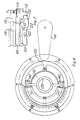
- FIG 1 shows a sample embodiment of the invention.
- This embodiment shows a wafer carrier 10 inside a vacuum load lock chamber 12.
- the wafer carrier 10 is also shown, in slightly greater detail, in Figure 4.
- the carrier 10 is shown with its door 14 standing open.
- the wafer carrier 10 is adapted to dock with a platform 18 (which is only partially visible in Figure 1, but is shown in more detail in Figure 4), so that, when a technician places a wafer carrier 10 inside the load lock 12, the position of the carrier 10 will be accurately known.
- the wafer carrier 10 has ears 16 which engage vertical slots 17 fixed to the position registration platform 18, so that the technician can slide the carrier into these slots until it rests on the platform 18, and thereby assure that the position of the carrier 10 is definitely known.
- the platform 18 includes two tapered pins 21 (one conical and one wedge-shaped) positioned to engage tapered holes 23 in the underside of the wafer carrier 10, but a wide variety of other arrangements could be used to assure mechanical registration, as will be obvious to any ordinarily skilled mechanical engineer.
- the carrier 10 preferably has a safety catch 15 on it which secures the door 14 from falling open. However, under normal conditions of transport this safety catch is not needed, since atmospheric pressure holds the door 14 shut against the internal vacuum of the carrier. When the carrier 10 is placed inside the load lock 12, a fixed finger 19 will push against the safety catch 15 to release it, so that the door 14 can be opened.
- the door 14 When the carrier 10 is docked with the platform 18, the door 14 will also be engaged with the door opening shaft 24.
- the door 14 has a shallow groove in its underside, which mates with a finger and arm 25 on the top of the door opening shaft 24.
- a high pressure purge (with dry nitrogen or other clean gas) is preferably applied through manifold 22 inside load lock lid 20.
- This high pressure purge provides vertical flow, to tend to transport particles downward, and also helps to blow off some of the large particles which will have collected on the wafer carrier 10 during its exposure to atmospheric conditions.
- This pump down stage is preferably relatively slow, in order not to stir up random particulates. That is, while low pressures do permit particles to fall from the air, those particles will still be available on the bottom of the chamber, and must not be stirred up if this can be avoided.
- a sloped bottom and/or polished sidewalls for the load lock, to reduce the population of particulates sticking to the sidewalls and bottom which can be sent flying by mechanical vibration.
- the present invention greatly reduces the problems of airborne particulates, which has always been the dominant type of particulate transport, so that the problem of ballistically transported particulates can now be usefully addressed.
- a related optional modification is the use of an insitu vacuum particle counter in the upper chamber, so that any increase in particle population in the critical volume can be detected.
- Such an in-situ particle counter can be built using a resonant circuit to measure charge transfer in a high-voltage vacuum-gap capacitor, or (for particles sufficiently large) by using a laser-driven optical cavity with a multiply-folded optical path. or by other means.
- this particulate sensor (or a second particulate sensor which is better adapted to sensing particulates at higher pressures) can be used to control the nitrogen shower prior to initial pumpdown. That is, instead of doing the nitrogen shower simply for a fixed duration, it may be protracted if the particulate monitor shows that the box was in an unusually dirty environment. It may even be desirable to pump the load lock down to a soft vacuum (using the roughing pump) and then bleed gas through the nitrogen shower ports, to create a downward flow. It may also be desirable to cycle the load lock from a soft vacuum (e.g.
- vacuum gauges 62 are preferably connected to the interior of the load lock chamber.
- the sensors 62 include a high-pressure gauge (such as a thermocouple), a low pressure gauge (such as an ionization gauge), and a differential sensor which accurately senses when the load lock interior pressure has been equalized with the atmosphere.
- a high-pressure gauge such as a thermocouple
- a low pressure gauge such as an ionization gauge
- a differential sensor which accurately senses when the load lock interior pressure has been equalized with the atmosphere.
- the pressures inside the wafer carrier 10 and the vacuum load lock 12 are more or less equalized, and the door 14 can be activated by operating motor 26, which is connected to door opening shaft 24 through vacuum feedthrough 25.
- Preferably two sensor switches are also included inside vacuum load lock 12, to ascertain when door 14 is in its fully opened position, and when door 14 is fully shut.
- door opening shaft 24 is rotated to open the door 14, until the sensor detects that the door is fully open.
- the transfer arm 28 is preferably kept in its home position at an elevation below the bottom of the door, so that the door 14 has clearance to open. After the sensor detects that the door 14 is fully open, the transfer arm can begin to operate.
- the transfer arm 28 preferably has two degrees of freedom. One direction of motion permits the transfer arm 28 to reach into carrier 10 or through port 30 into the adjacent processing chamber. The other degree of freedom corresponds to vertical motion of the transfer arm 28, which permits selection of which wafer inside the carrier 10 is to be removed, or which slot a wafer is to be placed into.
- an elevator drive motor 32 is used to control the elevation of the transfer arm 28, and arm drive motor 34 controls the extension and retraction of the transfer arm 28.
- both of these motors do not require vacuum feedthrough. but are housed inside the exhaust manifold 36 which leads from the load lock 12 to the vacuum pump 38, which may be, for example, a turbomolecular pump.
- the exhaust manifold 36 does not open directly into the load lock chamber 12, but instead has apertures 40 around its top. That is, the exhaust manifold 36 is preferably configured so that there is not any line of sight path from the drive motors 32 or 34 or from the pump 38 into the load lock chamber. This helps to reduce ballistic transport of particulates from these moving elements into the load lock chamber.
- the elevator drive motor 32 is preferably connected to drive a sub-platform 42 up and down, and the arm drive motor 34 is preferably mounted on this platform 42.
- a linkage is used inside the rotatable transfer arm support 44, to permit the transfer arm 28 to move very compactly.
- the transfer arm support 44 is preferably connected to a rotating rod which is driven by the arm drive motor 34, but the arm support 44 is preferably mounted on a tubular support 46 which does not rotate.
- An internal chain and sprocket linkage is preferably used so that the joint between arm support 44 and transfer arm 28 moves with twice the angular velocity of the joint between arm support 44 and tubular support 46.
- the transfer arm has 3 pins 50 on it to support the wafer.
- Each pin 50 preferably includes a small cone 52 on a small shoulder 54.
- the cone 52 and shoulder 54 are preferably made of a material which is soft enough to not scratch silicon.
- these portions (which are the only portions of transfer arm 28 which will actually touch the wafers being transported) are preferably made of a high-temperature plastic (i.e. a plastic with a relatively low propensity to outgas under vacuum) such as Ardel (a thermoplastic phenyl acrylate, made by Union Carbide) or Delrin.
- cones 52 at the center of the locating pins 50 permits very slight misalignments of the wafer to the transfer arm 28 to be corrected: in other words the system of wafer transport according to the present invention is a stable mechanical system, wherein small misalignments during successive operations will not accumulate, but will be damped out.
- one of the three pins 50 rests against the flat portion 56 of the wafer's circumference. This means that. in this embodiment, the three pins 50 on the transfer arm 28 do not define a circle of the same diameter as the diameter of the wafers 48 to be handled.
- the box 10 preferably has a flat surface on its interior back side which the flats 56 of the wafers 48 will rest against.
- a spring compression element on the inside surface of the door 14 pushes each wafer against this flat surface when the door 14 is closed, so that the wafers do not rattle around in transit. This also assures that, when the door 14 is opened, the location of the flat 56 on each wafer 48 is accurately known.
- elevator drive motor 32 is operated to bring the transfer arm 28 to just below the height of the first wafer which it is desired to remove, and arm drive motor 34 is then operated to extend the transfer arm 28 into the interior of the box 10.
- arm drive motor 34 is then operated to extend the transfer arm 28 into the interior of the box 10.
- the ledges 60 preferably have tapered surfaces rather than flat surfaces, so that contact between the ledges 60 and the wafer 48 resting on them is a line contact rather than an area contact, and is limited to the edge of the wafer. That is, in prior art wafer carriers area contact may be made over a substantial area, of many square millimeters, but the "line contact" used in the present invention makes contact only over a much smaller area, typically of a few square millimeters or less.
- An alternative definition of the "line contact” used in this embodiment of the invention is that the wafer support contacts the surface of the wafer only at points which are less than one millimeter from its edge.
- the desired wafer 48 will be picked up, and will be resting on the cones 52 or shoulders 54 of the three pins 50 on the transfer arm 28.
- larger diameter wafers will have greater thicknesses, but the present invention is eminently suited to such larger diameter wafers, since the size of the box 10 and the center spacing of the ledges 16 inside the box 10 can simply be scaled appropriately.
- the arm drive motor 34 is operated to bring the transfer arm 28 to the home position.
- the elevator drive motor 32 is then operated to bring the transfer arm 28 to a height where it can reach through the port 30.
- Port 30 is preferably covered by an isolation gate 31 unlike the gate 31 shown in Figure 3: the gate 31 preferably seals the port 30 without making sliding contact. (Again, the absence of sliding contact is advantageous to reduce internally generated particulates.)
- the isolation gate 31 over port 30 is preferably operated by an air cylinder, but a stepper motor may be used instead.
- a total of four motors are used: two which use vacuum feedthroughs, and two which are preferably contained inside the exhaust manifold 36.
- the arm drive motor is now operated again, to extend the transfer arm 28 through port 30 into the adjacent processing chamber.
- the adjacent processing chamber may be any one of many different kinds of processing stations.
- this station may be an implanter, a plasma etch, or a deposition station.
- the transfer arm reaching through the port 30 will place the wafer 48 on three pins 50, as shown in Figure 3, like those used in the transfer arm itself.
- the port 30 preferably has enough vertical height to permit some vertical travel while the arm 28 is extended through port 30, so that arm 28 can move vertically to lift a wafer from or deposit a wafer onto pins 50 inside the processing chamber.
- the processing chamber may include a fixture having spaced sloped ledges like the ledges 16 inside the transfer box, or may have other mechanical arrangements to receive the wafer.
- the arrangement used to receive the transferred wafer must have clearance on the underside of the wafer (at least at the time of transfer), so that the transfer arm 28 can reach in on the underside of the wafer to emplace or remove it.
- pins 50 are used to receive the transferred wafer, it may be desirable to provide a bellows motion or a vacuum feedthrough in order to provide vertical motion of the wafer support pins inside the processing chamber.
- a feedthrough may be provided to position the wafer 48 onto a susceptor after the transfer arm 28 has been withdrawn out of the way of the wafer.
- the processing chamber may be an engineering inspection station.
- a vacuum-isolated microscope objective lens will permit inspection of wafers in vacuum and (using an appropriately folded optical path) in a face-down position. This means that heavy use of engineer inspection can be made where appropriate, without the loss of engineer time and clean-room quality which can be caused by heavy traffic through a clean-room.
- the transfer arm 28 is preferably withdrawn, and the isolation gate over port 30 closed, while processing proceeds.
- the isolation gate over port 30 is opened again, the arm 28 is extended again, the elevator drive motor 32 is operated briefly so that the arm 28 picks up the wafer 48, and the arm drive motor 34 is again operated to bring the transfer arm 28 back into the home position.
- the elevator drive motor 32 is then operated to bring the transfer arm 28 to the correct height to align the wafer 48 with the desired slot inside the wafer carrier.
- the arm drive motor 34 is then operated to extend the transfer arm 28 into the wafer carrier 10, so that the wafer 48 which has just been processed is sitting above its pair of ledges 60.
- the elevator drive motor 32 is then briefly operated to lower the transfer arm 28, so that the wafer is resting on its own ledges 60, and the arm drive motor 34 is then operated to retract the transfer arm 28 to home position.
- the sequence of steps described above is then repeated, and the transfer arm 28 selects another wafer for processing.
- the wafers being transferred will move in exactly a straight line if the center to center lengths of transfer arm 28 and arm support 34 are equal. This is advantageous because it means that the side of the wafer being transferred will not bump or scrape against the sides of the box 10 when the wafer is being pulled out of or pushed into the box. That is, the clearances of the wafer carrier box can be relatively small (which helps to reduce particulate generation by rattling of the wafers during transport in the carrier) without risking particulate generation due to abrasion of the wafers against the metal box sides.
- the seals 13 will maintain a high vacuum in the carrier meanwhile, so that particulate transport to the wafer surfaces (and also adsorption of vapor-phase contaminants) is minimized.
- the wafer carrier also includes elastic elements 27 mounted in its door. These elastic elements exert light pressure against the wafers 48 when the door 14 is closed, and thus restrain them from rattling around and generating particulates.
- the elastic element 27 is configured as a set of springs in the embodiment shown, but other mechanical structures (e.g. a protruding bead of an elastic polymer) could alternatively be used to configure this.
- a flat contact surface 29 is preferably provided on the inner back surface of the wafer carrier box 10 for the slice flats to be pressed against.
- the ledges 60 on the sidewalls of the carrier box 10 are tapered. This helps to assure that contact with the supported surface of the wafer is made over a line only, rather than over any substantial area. This reduces wafer damage and particulate generation during transport. This also assists in damping out the accumulation of positioning errors, as discussed.
- the load lock lid 20 preferably has a window in it, to permit operator inspection of any possible mechanical jams.
- An advantage of the present invention is that, in the case of many possible mechanical malfunctions, the door of the wafer carrier 10 can be closed before attempts are made to correct the problem. For example, if somehow the transfer arm 28 picks up a wafer so that the wafer is not sitting properly on all three of the pins 50, the door drive motor 26 can be operated to close the door 14 before any attempts are made to correct the problem. Similarly, port 30 can be closed if the transfer arm 28 can be retracted into home position. It may be possible to correct some such mechanical misalignment problems simply by deviating from the normal control sequence.
- the position of a wafer 48 on transfer arm 28 may in some cases be adjusted by partially extending the transfer arm 28, so that the edge of wafer 48 just touches the outside of door 14, or of the isolation gate over port 30. If this does not work, the load lock 12 can be brought back up to atmospheric pressure (with the door 14 of wafer carrier 10 closed) and the load lock lid 20 opened so that the problem can be manually corrected.
- the wafer carrier 10 could be provided with a quick-connect vacuum fitting, to permit separate pumpdown on the carriers 10.
- this is omitted, since it is not necessary and since it simply provides another source of possible unreliability.
- load lock mechanism described need not be used solely with vacuum-tight wafer carriers, although that is the most preferred embodiment.
- This load lock can also be used with wafer carriers which carry atmospheric pressure inside. Although this is not the most preferred embodiment, it still carries substantial advantages, as is discussed above, over prior art load lock operations.
- a wafer carrier as described can be made in different sizes, to carry any desired number of wafers.
- a wafer carrier according to the present invention can be used to carry or store any desired number of wafers, up to its maximum. This provides additional flexibility in scheduling and process equipment logistics.
- FIG. 5 shows a sample further alternative embodiment wherein two load locks, each containing a wafer carrier 10, are both connected to a process module 102 which contains four process stations 104.
- the transfer arm 28 When the transfer arm 28 reaches through the port 30 from a load lock 12 into the process module 102, it places its wafer onto one of two wafer stages 106.
- These wafer stages 106 can be three pin supports or two ledge supports, or may have other mechanical configurations that would be obvious to those skilled in the art, as long as there is space underneath the supported wafer for the transfer arm 28 to lower free of the wafer and retract after it has placed the wafer on the supports. (It is preferable, however, that the wafer support used be such as to make line contact, rather than contact over any substantial area, to the under surface of the wafer.)
- Another transfer arm assembly 106 is provided inside the process module.
- This transfer arm assembly is generally similar to the transfer arm assembly 28, 44 and 46 used inside the load lock, but there are some differences.
- the transfer arm 28 used inside the load lock only needs to move wafers in a straight line.
- the transfer arm assembly 106 must also be able to move radially, to select any one of the process modules 104. Thus, an additional degree of freedom is needed.
- the reach of the transfer arm assembly 106 need not be the same as the transfer arm assemblies (28,44,46) used inside the load lock, and in fact the reach of transfer arm 106 is preferable larger, to permit adequate spacing of the process stations 104.
- the arm assembly 106 does not need as much travel in elevation as the transfer arms 28 used in the load locks.
- the transfer arm 128 will not have one of its three pins 50 resting on a wafer flat, so that the diameter of the circle defined by pins 50 is not the same for arms 28 and 128, even though they are handling wafers of the same diameter.
- the transfer arm assembly 106 is preferably essentially the same as the transfer arm assembly (28,44,46) used in the load lock, with these differences. By making the tubular support 46 rotatable and providing a third motor to drive this rotation, a third degree of freedom for the transfer arm is provided. Similarly, the dimensions of the transfer arm can simply be scaled as desired.
- transfer arm assembly 106 preferably includes a transfer arm 128 rotatably mounted on a transfer arm support 144.
- the transfer arm support 144 is pivotably mounted to a tubular support 146 (not shown), and an internal shaft, fixed to the transfer arm support 144, extends down through the tubular support 146.
- An internal chain drive with two to one gearing translates any differential rotation between tubular support 146 and arm support 144 into a further differential rotation (over twice as many degrees) between arm support 144 and transfer arm 128.
- An arm drive motor mounted below the transport assembly 106, is connected to rotate the shaft which is fixed to arm support 144.
- An arm rotation motor is connected to rotate the tubular support 146.
- an elevator mechanism provides vertical motion of the transfer arm assembly 106.
- the vertical motion required of assembly 106 is not typically as much as that required of the transfer arms 28 in the load locks 12, since the transfer arm 128 will typically not need to select one of several vertically separated wafer positions like those in the wafer carrier 10, but will typically merely be used to pick and place wafers from a number of possible wafer stations which are all on the same plane.
- the vertical elevation of the transfer 128 could be controlled by an air cylinder rather than by an elevator motor assembly as discussed above.
- the transfer arm assembly 106 can be rotated without being extended.
- the tubular support 146 can be held fixed while the arm support 144 is rotated, and this will cause the transfer arm 128 to extend as described above.
- the transfer arm assembly 106 is rotated (if necessary), extended at a low position so that transfer arm 128 comes underneath the wafer, elevated so that transfer arm 128 picks up the wafer, and retracted to its home position.
- the assembly 106 is then rotated again, and the transfer arm 128 is extended, so that the wafer is now located above a wafer support in one of the process stations 104, or above the other wafer stage 106.
- the wafer can now be placed on the wafer support or wafer transfer stage, and the arm 128 can now be retracted.
- the process station 104 can now be sealed off from the main process module 102, and separate single-wafer processing of the wafer can begin. Meanwhile, the transfer arms 128 and 28 can perform other operations. When a wafer in a module 104 has completed processing, that process station 104 can then be pumped down to the same low pressure as the interior of process module 102, and process station 104 can be opened. The transfer arm assembly 106 can now be operated to remove this wafer, and transfer it either to one of the wafer stages 106 or to another one of the process modules 104.
- One advantage of the present invention is that the process modules 104 can all be configured to do the same operation, which will permit wafer transport-limited throughput (even for fairly slow processing operations), if there is a sufficient number of process stations 104 in the process module 102: or, alternatively, different operations can be used in different ones of the process stations 104.
- the present invention permits the use of sequential processing, which is increasingly recognized as desirable, since processing variations caused by adsorbed contaminants or by native oxide are eliminated.
- two of the process stations 104 can be configured for oxide growth, one for nitride deposition, and one for poly deposition, to permit complete in-situ fabrication of oxynitride poly-to-poly capacitors.
- the provision of different process steps in the different stations 104 means that many lot splits and process variations can be performed simply by programming the appropriate operations, without relying on technicians to correctly identify which wafers should go to which machines.
- the capability to have different operations proceed in different ones of the process stations 104 provides additional processing flexibility.
- the overall wafer transfer sequence is completely arbitrary, and may be selected as desired.
- the wafers from one wafer carrier 10 could be completely processed and returned to that wafer carrier 10, and the load lock 12 containing the just-processed wafers could be sealed off from process module 102, so that the wafers in the other wafer carrier 10 in the other load lock 12 could be processed while a technician removed the carrier full of processed wafers from the other load lock 12.
- the programmability and random access of this arrangement could be used to shuffle and interchange wafers between the two carriers 10 in whatever fashion desired.
- this arrangement is not at all limited to two load locks 12 nor to four process stations 104, but the arrangement described can be scaled to other numbers of process stations 104 in a module 102, or other numbers of load locks 12 attached to a module 102, or to use of more than one transfer arm assembly 106 inside a module, if desired.
- Figure 6 shows a sample process station 104, which can be used in a structure such as shown in Figure 5.
- Figure 6 shows a single slice reactor which can be used for reactive ion etching or for plasma etching.
- the transfer arm 128 places a wafer onto tapered Ardel pins 50, and then retracts.
- the whole lower assembly including the chamber 112, ground electrode 110, gas distributor 120, base plate 138, and top plate 114 are moved upward, using, e.g., an air cylinder or a vacuum feed through (not shown).
- a bellows 124 permits this vertical motion to occur while maintaining a vacuum-tight interface to the interior of the module 102.
- a helium bleed port 134 is provided to connect a helium supply to the back of the wafer.
- This helium space means that the space between the low points of the powered electrode 118 and the wafer will be filled with helium, rather than vacuum. and this assure a reasonably low-thermal-resistance and highly repeatable thermal contact between the wafer and the powered electrode 118.
- Powered electrode 118 preferably includes coolant manifold spaces 136, to which coolant can be supplied.
- the tapered pins 50 are not mounted on sliding pin supports 130 supported by elastic elements 132, but are fixed. Since the helium bleed 134 assures good thermal contact between the back side of the wafer and the surface of the powered electrode 118, a tolerance of several thousands of an inch will still permit good rf coupling of the electrode 118 to the wafer, and still permit good thermal contact between the electrode 118 and the wafer. A tolerance of this magnitude should provide enough allowance for thermal expansions of chamber walls, variation in seal thickness, variation in wafer thickness, etc., to still permit reliable sealing of the lower chamber portion to the upper portion.
- the quartz faces 114 and 116 would preferably be shaped slightly differently, to minimize the lateral spread of the plasma adjacent to the face of the wafer.
- the presently preferred embodiment does use sliding pin supports 130, since they permit the quartz piece 114 to confine the plasma closely near the face of the wafer 48 as shown in Figure 7.
- Figure 7 shows the upper portion of the process station of Figure 6, in the closed position, with a wafer 48 held therein for processing.
- the helium bleed can be started through port 134.
- desired process gasses can be provided through a process gas distributor 120.
- the process gas distributor 120 is made of quartz, so that it does not pick up eddy currents from the rf power present. Moreover, since the surface of the quartz is highly insulating, the plasma boundary near the quartz will not have as much voltage nor as much current across it as the plasma boundary near a grounded conductive element would. This means that plasma-assisted reactions near the quartz will not occur at as high a rate as they would near a grounded conductive element, so that deposition is reduced.
- quartz is a fairly good thermal insulator, and the temperature of the susceptor may therefore be raised (by radiation from the plasma) to 100 or 200 degrees C. This is advantageous, since raising the temperature of the distributor will further reduce deposition on it.
- the generated plasma will fill the chamber between powered electrode 118 and ground electrode 110 fairly uniformly.
- the gas distributor 120 protrudes into the densest part of the plasma.
- the gas distributor 120 is preferably a ring, of perhaps one-half the diameter of the wafer being processed, with hollow supports which lead down to gas connections 140 mounted in the base plate 138.
- a quick-connect mounting is provided for the quartz distributor 120, so it can rapidly and easily be changed out as desired.
- the gas distributor 120 is, in the presently preferred embodiment, spaced away from the surface of the wafer by about four centimeters. This spacing, and the exact shape of the gas distributor 120, and the spacing of the ports 122 on the gas distributor, are none of them critical. These parameters can be changed if desired, but, if modified, they should be selected so that diffusion of process gasses and process gas products from the ports 122 in the gas distributor 120 provides: 1) diffusion-dominated transport of the process gasses and process gas products to the plasma boundary at the face of the wafer 48: and 2) a fairly uniform concentration of process gasses and process gas products at the plasma boundary next to the face of wafer 48. For example, the spacing of the distributor away from the wafer face could be anywhere in the range from one to fifteen cm.
- the ground plane electrode 110 is preferably cooled, using coolant lines 150 connected to manifold cavities inside the electrode 110. If additional cooling is needed, the walls 112 may also be cooled.
- lines 150 are preferably flexible hoses, to accommodate the vertical travel of the whole lower etching chamber (110, 112, 138, 120, 114) as described above.
- the gas supply tube 150 which supplies process gasses through connection 140 to the gas distributor 120, is preferably also flexible for the same reason. If flexure of these hoses is found to generate excess particulates, a gas feed outside the bellows 124, through the side of the base plate 138, could be used instead.
- Figure 8 shows a plan view of the reactor of Figure 6.
- the shape of the gas distributor 120 can be seen more clearly in this plan view. It can also be seen that the base plate 138 includes substantial spaces around the edge of the ground electrode 110, which provide a passage from the gas feed ports 122 to a vacuum pump below.
- the overall gas flow in this reactor is downward, away from the face of the wafer, which assists in reducing particulates.
- a holding time may then be interposed, for thermal stabilization of the process station or for release of possible suspended particulates, and then the process station 104 is opened and the transfer arm assembly 106 operates as before to remove the wafer from it.
- the present invention provides all of the advantages listed above. and others besides.
- the present invention can be very widely modified and varied, and its scope is not limited except as specified in the claims.
Description
Claims (8)
- A method of processing wafers (48) having an active face comprising the steps of:wherein each wafer processing station (104) can be sealed off from the processing module chamber (102) thus allowing for single-wafer processing.transporting a plurality of wafers (48) with the active face down to or from a vacuum-sealable load lock (12) by means of a wafer carrier (10), which load lock (12) opens into a vacuum-sealable processing module chamber (102), containing a plurality of wafer processing stations (104),creating a vacuum within said module chamber (102) and said load lock (12), and transferring to and from said load lock (12) by means of a transfer arm (28) said wafers (48) with the active face down, one at a time, through portions of said module chamber (102) to or from selected processing stations (104),
- The method of claim 1, further comprising the steps of:
processing said wafers (48) at said selected processing stations (104) while said wafers (48) are in an orientation with the active face down. - The method of claim 1 or 2, wherein said step of transporting said plurality of wafers (48), includes the step of maintaining said wafers (48) under vacuum during transport.
- The method of claim 1, 2, or 3, further comprising the step of:
maintaining said wafers (48) in a hard vacuum environment during all of said steps. - A module for processing wafers (48) having an active face comprising:a vacuum-tight processing module chamber (102) containing a plurality of wafer processing stations (104), wherein each of said wafer processing stations (104) can be sealed off from said processing module chamber (102), thus allowing for single-wafer processing;at least one load lock (12) opening into said module chamber (102), said at least one load lock (12) having space therein to hold a wafer carrier (10) for holding a plurality of wafers (48) with the active face down;a vacuum pump means connected to the module for creating a vacuum within said module chamber (102) and said at least one load lock (12); anda wafer transfer arm (28) for transferring of wafers (48) with the active face down to and from said plurality of processing stations (104) to and from said load lock (12).
- The module of claim 5, wherein said wafer carrier (10) is vacuum sealable for maintaining a vacuum within said carrier (10).
- The module of claim 5 or 6, wherein said wafer carrier (10) includes means for holding said plurality of wafers spaced apart one from the other in a vertical column.
- The module of claim 7, wherein said wafer transfer arm (28) is elevatable vertically to access individual wafers in said vertical column of wafers in said wafer carrier.
Applications Claiming Priority (5)
| Application Number | Priority Date | Filing Date | Title |
|---|---|---|---|
| US79070885A | 1985-10-24 | 1985-10-24 | |
| US06/790,924 US4687542A (en) | 1985-10-24 | 1985-10-24 | Vacuum processing system |
| US790708 | 1985-10-24 | ||
| US790924 | 1985-10-24 | ||
| EP86114386A EP0219826B1 (en) | 1985-10-24 | 1986-10-17 | Vacuum processing system |
Related Parent Applications (2)
| Application Number | Title | Priority Date | Filing Date |
|---|---|---|---|
| EP86114386A Division EP0219826B1 (en) | 1985-10-24 | 1986-10-17 | Vacuum processing system |
| EP86114386.5 Division | 1986-10-17 |
Publications (3)
| Publication Number | Publication Date |
|---|---|
| EP0555891A2 EP0555891A2 (en) | 1993-08-18 |
| EP0555891A3 EP0555891A3 (en) | 1993-09-15 |
| EP0555891B1 true EP0555891B1 (en) | 1999-01-20 |
Family
ID=27121066
Family Applications (3)
| Application Number | Title | Priority Date | Filing Date |
|---|---|---|---|
| EP93106892A Expired - Lifetime EP0555890B1 (en) | 1985-10-24 | 1986-10-17 | Wafer transfer arm and method |
| EP86114386A Expired - Lifetime EP0219826B1 (en) | 1985-10-24 | 1986-10-17 | Vacuum processing system |
| EP93106893A Expired - Lifetime EP0555891B1 (en) | 1985-10-24 | 1986-10-17 | Vacuum processing system and method |
Family Applications Before (2)
| Application Number | Title | Priority Date | Filing Date |
|---|---|---|---|
| EP93106892A Expired - Lifetime EP0555890B1 (en) | 1985-10-24 | 1986-10-17 | Wafer transfer arm and method |
| EP86114386A Expired - Lifetime EP0219826B1 (en) | 1985-10-24 | 1986-10-17 | Vacuum processing system |
Country Status (3)
| Country | Link |
|---|---|
| EP (3) | EP0555890B1 (en) |
| JP (5) | JPS62181440A (en) |
| DE (3) | DE3650057T2 (en) |
Cited By (4)
| Publication number | Priority date | Publication date | Assignee | Title |
|---|---|---|---|---|
| US7258520B2 (en) | 2002-08-31 | 2007-08-21 | Applied Materials, Inc. | Methods and apparatus for using substrate carrier movement to actuate substrate carrier door opening/closing |
| US7299831B2 (en) | 2002-08-31 | 2007-11-27 | Applied Materials, Inc. | Substrate carrier having door latching and substrate clamping mechanisms |
| US7720558B2 (en) | 2004-09-04 | 2010-05-18 | Applied Materials, Inc. | Methods and apparatus for mapping carrier contents |
| US8074597B2 (en) | 2006-01-11 | 2011-12-13 | Applied Materials, Inc. | Methods and apparatus for purging a substrate carrier |
Families Citing this family (35)
| Publication number | Priority date | Publication date | Assignee | Title |
|---|---|---|---|---|
| US4917556A (en) * | 1986-04-28 | 1990-04-17 | Varian Associates, Inc. | Modular wafer transport and processing system |
| GB2194500B (en) * | 1986-07-04 | 1991-01-23 | Canon Kk | A wafer handling apparatus |
| EP0303030A1 (en) * | 1987-07-16 | 1989-02-15 | Texas Instruments Incorporated | Processing apparatus and method |
| JPS6428912A (en) * | 1987-07-24 | 1989-01-31 | Hitachi Electr Eng | Wafer handling device |
| DE3735449A1 (en) * | 1987-10-20 | 1989-05-03 | Convac Gmbh | MANUFACTURING SYSTEM FOR SEMICONDUCTOR SUBSTRATES |
| JP2926593B2 (en) * | 1988-02-12 | 1999-07-28 | 東京エレクトロン株式会社 | Substrate processing apparatus, resist processing apparatus, substrate processing method, and resist processing method |
| US4949783A (en) * | 1988-05-18 | 1990-08-21 | Veeco Instruments, Inc. | Substrate transport and cooling apparatus and method for same |
| IL86514A0 (en) * | 1988-05-26 | 1988-11-15 | ||
| DE3822598C2 (en) * | 1988-07-04 | 1997-09-04 | Siemens Ag | Adjustment arrangement and method for adjusting a gripping device of a robot arm for handling a semiconductor wafer |
| EP0367423A3 (en) * | 1988-10-31 | 1991-01-09 | Eaton Corporation | Vacuum deposition system |
| US6989228B2 (en) | 1989-02-27 | 2006-01-24 | Hitachi, Ltd | Method and apparatus for processing samples |
| US6077788A (en) * | 1989-02-27 | 2000-06-20 | Hitachi, Ltd. | Method and apparatus for processing samples |
| US5868854A (en) | 1989-02-27 | 1999-02-09 | Hitachi, Ltd. | Method and apparatus for processing samples |
| JP2528962B2 (en) * | 1989-02-27 | 1996-08-28 | 株式会社日立製作所 | Sample processing method and device |
| NL8901630A (en) * | 1989-06-28 | 1991-01-16 | Philips Nv | VACUUM SYSTEM. |
| JP2767142B2 (en) * | 1989-10-18 | 1998-06-18 | 東京エレクトロン株式会社 | Unit for vacuum processing equipment |
| JP2525284B2 (en) * | 1990-10-22 | 1996-08-14 | ティーディーケイ株式会社 | Clean transfer method and device |
| JPH05251408A (en) * | 1992-03-06 | 1993-09-28 | Ebara Corp | Etching system |
| US5398481A (en) * | 1992-05-19 | 1995-03-21 | Ebara Corporation | Vacuum processing system |
| KR100303075B1 (en) | 1992-11-06 | 2001-11-30 | 조셉 제이. 스위니 | Integrated circuit wafer transfer method and apparatus |
| EP0596536A1 (en) * | 1992-11-06 | 1994-05-11 | Applied Materials, Inc. | Transport system and method of using same |
| US5643366A (en) * | 1994-01-31 | 1997-07-01 | Applied Materials, Inc. | Wafer handling within a vacuum chamber using vacuum |
| GB2320135A (en) * | 1996-12-04 | 1998-06-10 | Smiths Industries Plc | Semiconductor wafer processing apparatus |
| JP3850951B2 (en) * | 1997-05-15 | 2006-11-29 | 東京エレクトロン株式会社 | Substrate transport apparatus and substrate transport method |
| US7018517B2 (en) | 2002-06-21 | 2006-03-28 | Applied Materials, Inc. | Transfer chamber for vacuum processing system |
| TW200524073A (en) | 2003-11-13 | 2005-07-16 | Applied Materials Inc | Kinematic pin with shear member and substrate carrier for use therewith |
| DE10359464A1 (en) * | 2003-12-17 | 2005-07-28 | Fraunhofer-Gesellschaft zur Förderung der angewandten Forschung e.V. | Method and device for generating in particular EUV radiation and / or soft X-radiation |
| US7849889B2 (en) * | 2006-05-31 | 2010-12-14 | Philip Morris Usa Inc. | Applicator wheel for filling cavities with metered amounts of particulate material |
| JP5329853B2 (en) | 2008-06-25 | 2013-10-30 | ティアック株式会社 | Optical disc apparatus and optical disc processing system having the same |
| JP5329854B2 (en) | 2008-06-25 | 2013-10-30 | ティアック株式会社 | Optical disc apparatus and optical disc processing system having the same |
| WO2011142000A1 (en) | 2010-05-11 | 2011-11-17 | トヨタ自動車株式会社 | Vehicle shift controller |
| KR102139673B1 (en) * | 2013-07-04 | 2020-07-31 | 엘지디스플레이 주식회사 | Apparatus for fabricathing flat panel display device and operating method thereof |
| JP2017204608A (en) * | 2016-05-13 | 2017-11-16 | 信越ポリマー株式会社 | Substrate storage container |
| US11891685B2 (en) * | 2019-07-22 | 2024-02-06 | Ulvac, Inc. | Vacuum processing apparatus |
| WO2021192001A1 (en) * | 2020-03-24 | 2021-09-30 | 株式会社日立ハイテク | Vacuum processing device |
Citations (1)
| Publication number | Priority date | Publication date | Assignee | Title |
|---|---|---|---|---|
| EP0152555A2 (en) * | 1984-02-21 | 1985-08-28 | Plasma-Therm, Inc. | Apparatus for conveying a semiconductor wafer |
Family Cites Families (30)
| Publication number | Priority date | Publication date | Assignee | Title |
|---|---|---|---|---|
| JPS5337546U (en) * | 1976-09-06 | 1978-04-01 | ||
| JPS5337456U (en) * | 1976-09-07 | 1978-04-01 | ||
| US4181161A (en) * | 1977-02-02 | 1980-01-01 | Balzers Aktiengesellschaft Fur Hochvakuumtechnik Und Dunne Schichten | Method of producing a high vacuum in a container |
| JPS5480086A (en) * | 1977-12-09 | 1979-06-26 | Hitachi Ltd | Mask aligner |
| US4293249A (en) * | 1980-03-03 | 1981-10-06 | Texas Instruments Incorporated | Material handling system and method for manufacturing line |
| JPS5730341A (en) * | 1980-07-30 | 1982-02-18 | Anelva Corp | Substrate processing device |
| JPS5739914A (en) * | 1980-08-25 | 1982-03-05 | Shimizu Construction Co Ltd | Method of controlling moisture of high slump concrete |
| JPS57113245A (en) * | 1980-12-29 | 1982-07-14 | Fujitsu Ltd | Sample conveying method into vacuum device |
| US4433951A (en) * | 1981-02-13 | 1984-02-28 | Lam Research Corporation | Modular loadlock |
| JPS57145321A (en) * | 1981-03-03 | 1982-09-08 | Nec Corp | Dry etching device |
| JPS57149748A (en) * | 1981-03-12 | 1982-09-16 | Anelva Corp | Treating device for substrate |
| US4466766A (en) * | 1981-05-20 | 1984-08-21 | Ruska Instrument Corporation | Transfer apparatus |
| JPS57194531A (en) * | 1981-05-26 | 1982-11-30 | Toshiba Corp | Electron beam transfer device |
| JPS58292U (en) * | 1981-06-26 | 1983-01-05 | 同和機器工業株式会社 | Cooling and freezing equipment |
| JPS58127341A (en) * | 1982-01-25 | 1983-07-29 | Hitachi Ltd | Automatic wafer handling apparatus |
| JPS58170028A (en) * | 1982-03-31 | 1983-10-06 | Fujitsu Ltd | Vacuum treating device |
| DE3214256A1 (en) * | 1982-04-17 | 1983-10-20 | Licentia Patent-Verwaltungs-Gmbh, 6000 Frankfurt | Device for handling a substrate |
| JPS58204347A (en) * | 1982-05-24 | 1983-11-29 | Nippon Jido Seigyo Kk | Automatic loader of specimen used for defect inspection device of pattern |
| DE3219502C2 (en) * | 1982-05-25 | 1990-04-19 | Ernst Leitz Wetzlar Gmbh, 6330 Wetzlar | Device for the automatic transport of disc-shaped objects |
| JPS58213429A (en) * | 1982-06-07 | 1983-12-12 | Nec Corp | Dry etching device |
| JPS5956739A (en) * | 1982-09-27 | 1984-04-02 | Ulvac Corp | Wafer loading apparatus |
| JPS5994435A (en) * | 1982-11-20 | 1984-05-31 | Tokuda Seisakusho Ltd | Vacuum treating device |
| JPS59186326A (en) * | 1983-04-06 | 1984-10-23 | Hitachi Ltd | Dry-etching apparatus |
| JPS59208837A (en) * | 1983-05-13 | 1984-11-27 | Nec Kyushu Ltd | Plasma etching device |
| US4534695A (en) * | 1983-05-23 | 1985-08-13 | Eaton Corporation | Wafer transport system |
| JPS6020515A (en) * | 1983-07-14 | 1985-02-01 | Ulvac Corp | Sputtering etching device |
| JPS6054449A (en) * | 1983-09-05 | 1985-03-28 | Toshiba Corp | Conveying jig for semiconductor wafer |
| EP0151336B1 (en) * | 1983-09-28 | 1991-01-02 | Hewlett-Packard Company | System for integrated circuit processing |
| JPS60102744A (en) * | 1983-11-09 | 1985-06-06 | Hitachi Ltd | Vacuum treater |
| JPS60175411A (en) * | 1984-02-22 | 1985-09-09 | Hitachi Ltd | Manufacture of thin semiconductor film and apparatus thereof |
-
1986
- 1986-10-17 DE DE19863650057 patent/DE3650057T2/en not_active Expired - Fee Related
- 1986-10-17 EP EP93106892A patent/EP0555890B1/en not_active Expired - Lifetime
- 1986-10-17 EP EP86114386A patent/EP0219826B1/en not_active Expired - Lifetime
- 1986-10-17 DE DE19863650710 patent/DE3650710T2/en not_active Expired - Fee Related
- 1986-10-17 DE DE19863650697 patent/DE3650697T2/en not_active Expired - Fee Related
- 1986-10-17 EP EP93106893A patent/EP0555891B1/en not_active Expired - Lifetime
- 1986-10-24 JP JP61253518A patent/JPS62181440A/en active Granted
-
1991
- 1991-05-07 JP JP10134791A patent/JPH04226049A/en active Pending
-
1993
- 1993-03-08 JP JP4673493A patent/JPH0645425A/en not_active Withdrawn
- 1993-03-08 JP JP5046733A patent/JP2693352B2/en not_active Expired - Fee Related
- 1993-04-26 JP JP5099635A patent/JPH0629369A/en not_active Withdrawn
Patent Citations (1)
| Publication number | Priority date | Publication date | Assignee | Title |
|---|---|---|---|---|
| EP0152555A2 (en) * | 1984-02-21 | 1985-08-28 | Plasma-Therm, Inc. | Apparatus for conveying a semiconductor wafer |
Cited By (6)
| Publication number | Priority date | Publication date | Assignee | Title |
|---|---|---|---|---|
| US7258520B2 (en) | 2002-08-31 | 2007-08-21 | Applied Materials, Inc. | Methods and apparatus for using substrate carrier movement to actuate substrate carrier door opening/closing |
| US7299831B2 (en) | 2002-08-31 | 2007-11-27 | Applied Materials, Inc. | Substrate carrier having door latching and substrate clamping mechanisms |
| US7720558B2 (en) | 2004-09-04 | 2010-05-18 | Applied Materials, Inc. | Methods and apparatus for mapping carrier contents |
| US8074597B2 (en) | 2006-01-11 | 2011-12-13 | Applied Materials, Inc. | Methods and apparatus for purging a substrate carrier |
| US8601975B2 (en) | 2006-01-11 | 2013-12-10 | Applied Materials, Inc. | Methods and loadport apparatus for purging a substrate carrier |
| US8689812B2 (en) | 2006-01-11 | 2014-04-08 | Applied Materials, Inc. | Methods and loadport for purging a substrate carrier |
Also Published As
| Publication number | Publication date |
|---|---|
| EP0555891A2 (en) | 1993-08-18 |
| EP0219826B1 (en) | 1994-09-07 |
| EP0219826A2 (en) | 1987-04-29 |
| JPH04226049A (en) | 1992-08-14 |
| EP0555890B1 (en) | 1998-09-02 |
| DE3650697D1 (en) | 1998-10-08 |
| JPS62181440A (en) | 1987-08-08 |
| DE3650710T2 (en) | 1999-08-19 |
| EP0555890A3 (en) | 1993-09-15 |
| DE3650057D1 (en) | 1994-10-13 |
| JPH0556859B2 (en) | 1993-08-20 |
| JPH0629369A (en) | 1994-02-04 |
| DE3650057T2 (en) | 1995-02-16 |
| JPH0658931B1 (en) | 1994-08-03 |
| EP0219826A3 (en) | 1989-07-26 |
| DE3650710D1 (en) | 1999-03-04 |
| EP0555891A3 (en) | 1993-09-15 |
| EP0555890A2 (en) | 1993-08-18 |
| DE3650697T2 (en) | 1999-04-15 |
| JPH0640517A (en) | 1994-02-15 |
| JPH0658932B1 (en) | 1994-08-03 |
| JPH0645425A (en) | 1994-02-18 |
| JP2693352B2 (en) | 1997-12-24 |
Similar Documents
| Publication | Publication Date | Title |
|---|---|---|
| EP0555891B1 (en) | Vacuum processing system and method | |
| US4687542A (en) | Vacuum processing system | |
| US5044871A (en) | Integrated circuit processing system | |
| US4966519A (en) | Integrated circuit processing system | |
| US4816116A (en) | Semiconductor wafer transfer method and arm mechanism | |
| US4842680A (en) | Advanced vacuum processor | |
| JP7263639B2 (en) | Substrate transfer section | |
| US5586585A (en) | Direct loadlock interface | |
| US4916091A (en) | Plasma and plasma UV deposition of SiO2 | |
| US6578287B2 (en) | Substrate cooling system and method | |
| US5931631A (en) | Method and apparatus for vertical transfer of a semiconductor wafer cassette | |
| US20010038783A1 (en) | Dual loading port semiconductor processing equipment | |
| KR100729699B1 (en) | Clean device with clean box-opening/closing device | |
| US20210202283A1 (en) | Loadlock Module and Semiconductor Manufacturing Apparatus Including the Same | |
| US4943457A (en) | Vacuum slice carrier | |
| US4882299A (en) | Deposition of polysilicon using a remote plasma and in situ generation of UV light. | |
| JP2545591B2 (en) | Wafer processing equipment | |
| JPH05304197A (en) | Multi-chamber system | |
| JP2625112B2 (en) | Method for storing processed wafers under desired vacuum conditions | |
| JP2540524B2 (en) | Wafer support | |
| JPH0653304A (en) | Low-pressure processing device | |
| JP3160691B2 (en) | Processing equipment | |
| US20010041121A1 (en) | Single chamber vacuum processing tool | |
| JP2839830B2 (en) | Manufacturing method of integrated circuit | |
| JPH07201951A (en) | Processing apparatus and application thereof |
Legal Events
| Date | Code | Title | Description |
|---|---|---|---|
| PUAI | Public reference made under article 153(3) epc to a published international application that has entered the european phase |
Free format text: ORIGINAL CODE: 0009012 |
|
| PUAL | Search report despatched |
Free format text: ORIGINAL CODE: 0009013 |
|
| AC | Divisional application: reference to earlier application |
Ref document number: 219826 Country of ref document: EP |
|
| AK | Designated contracting states |
Kind code of ref document: A2 Designated state(s): DE FR GB NL |
|
| AK | Designated contracting states |
Kind code of ref document: A3 Designated state(s): DE FR GB NL |
|
| RIN1 | Information on inventor provided before grant (corrected) |
Inventor name: HILDENBRAND, RANDALL C. Inventor name: MATTHEWS, ROBERT Inventor name: SPENCER, JOHN E. Inventor name: CARTER, DUANE E. Inventor name: WOOLDRIDGE, TIMOTHY A. Inventor name: DAVIS, CECIL |
|
| 17P | Request for examination filed |
Effective date: 19940309 |
|
| 17Q | First examination report despatched |
Effective date: 19950210 |
|
| GRAG | Despatch of communication of intention to grant |
Free format text: ORIGINAL CODE: EPIDOS AGRA |
|
| GRAG | Despatch of communication of intention to grant |
Free format text: ORIGINAL CODE: EPIDOS AGRA |
|
| GRAH | Despatch of communication of intention to grant a patent |
Free format text: ORIGINAL CODE: EPIDOS IGRA |
|
| GRAH | Despatch of communication of intention to grant a patent |
Free format text: ORIGINAL CODE: EPIDOS IGRA |
|
| GRAA | (expected) grant |
Free format text: ORIGINAL CODE: 0009210 |
|
| AC | Divisional application: reference to earlier application |
Ref document number: 219826 Country of ref document: EP |
|
| AK | Designated contracting states |
Kind code of ref document: B1 Designated state(s): DE FR GB NL |
|
| REF | Corresponds to: |
Ref document number: 3650710 Country of ref document: DE Date of ref document: 19990304 |
|
| PG25 | Lapsed in a contracting state [announced via postgrant information from national office to epo] |
Ref country code: DE Free format text: LAPSE BECAUSE OF FAILURE TO SUBMIT A TRANSLATION OF THE DESCRIPTION OR TO PAY THE FEE WITHIN THE PRESCRIBED TIME-LIMIT Effective date: 19990421 |
|
| ET | Fr: translation filed | ||
| PLBE | No opposition filed within time limit |
Free format text: ORIGINAL CODE: 0009261 |
|
| STAA | Information on the status of an ep patent application or granted ep patent |
Free format text: STATUS: NO OPPOSITION FILED WITHIN TIME LIMIT |
|
| 26N | No opposition filed | ||
| REG | Reference to a national code |
Ref country code: GB Ref legal event code: IF02 |
|
| PGFP | Annual fee paid to national office [announced via postgrant information from national office to epo] |
Ref country code: GB Payment date: 20030915 Year of fee payment: 18 |
|
| PGFP | Annual fee paid to national office [announced via postgrant information from national office to epo] |
Ref country code: NL Payment date: 20030916 Year of fee payment: 18 |
|
| PGFP | Annual fee paid to national office [announced via postgrant information from national office to epo] |
Ref country code: FR Payment date: 20031003 Year of fee payment: 18 |
|
| PGFP | Annual fee paid to national office [announced via postgrant information from national office to epo] |
Ref country code: DE Payment date: 20031031 Year of fee payment: 18 |
|
| PG25 | Lapsed in a contracting state [announced via postgrant information from national office to epo] |
Ref country code: GB Free format text: LAPSE BECAUSE OF NON-PAYMENT OF DUE FEES Effective date: 20041017 |
|
| PG25 | Lapsed in a contracting state [announced via postgrant information from national office to epo] |
Ref country code: NL Free format text: LAPSE BECAUSE OF NON-PAYMENT OF DUE FEES Effective date: 20050501 |
|
| GBPC | Gb: european patent ceased through non-payment of renewal fee |
Effective date: 20041017 |
|
| PG25 | Lapsed in a contracting state [announced via postgrant information from national office to epo] |
Ref country code: FR Free format text: LAPSE BECAUSE OF NON-PAYMENT OF DUE FEES Effective date: 20050630 |
|
| NLV4 | Nl: lapsed or anulled due to non-payment of the annual fee |
Effective date: 20050501 |
|
| REG | Reference to a national code |
Ref country code: FR Ref legal event code: ST |