EP0555660A2 - Apparatus for interlayer planarization of semiconductor material - Google Patents
Apparatus for interlayer planarization of semiconductor material Download PDFInfo
- Publication number
- EP0555660A2 EP0555660A2 EP93100667A EP93100667A EP0555660A2 EP 0555660 A2 EP0555660 A2 EP 0555660A2 EP 93100667 A EP93100667 A EP 93100667A EP 93100667 A EP93100667 A EP 93100667A EP 0555660 A2 EP0555660 A2 EP 0555660A2
- Authority
- EP
- European Patent Office
- Prior art keywords
- layer
- planarizing
- pad
- psi
- subsurface
- Prior art date
- Legal status (The legal status is an assumption and is not a legal conclusion. Google has not performed a legal analysis and makes no representation as to the accuracy of the status listed.)
- Granted
Links
- 239000004065 semiconductor Substances 0.000 title claims abstract description 39
- 239000000463 material Substances 0.000 title claims description 72
- 239000011229 interlayer Substances 0.000 title description 2
- 230000002706 hydrostatic effect Effects 0.000 claims abstract description 31
- 238000005498 polishing Methods 0.000 claims description 32
- 239000011248 coating agent Substances 0.000 claims description 22
- 238000000576 coating method Methods 0.000 claims description 22
- 239000002002 slurry Substances 0.000 claims description 15
- 239000012858 resilient material Substances 0.000 claims description 6
- 238000010348 incorporation Methods 0.000 claims 2
- 239000004005 microsphere Substances 0.000 claims 2
- 239000007788 liquid Substances 0.000 claims 1
- 239000010410 layer Substances 0.000 description 58
- 229910052751 metal Inorganic materials 0.000 description 27
- 239000002184 metal Substances 0.000 description 27
- 238000000034 method Methods 0.000 description 9
- 239000002131 composite material Substances 0.000 description 8
- 230000006835 compression Effects 0.000 description 8
- 238000007906 compression Methods 0.000 description 8
- 239000007789 gas Substances 0.000 description 8
- 229920002120 photoresistant polymer Polymers 0.000 description 8
- 229910044991 metal oxide Inorganic materials 0.000 description 7
- 239000000853 adhesive Substances 0.000 description 5
- 230000001070 adhesive effect Effects 0.000 description 5
- 150000004706 metal oxides Chemical class 0.000 description 5
- VYPSYNLAJGMNEJ-UHFFFAOYSA-N Silicium dioxide Chemical compound O=[Si]=O VYPSYNLAJGMNEJ-UHFFFAOYSA-N 0.000 description 4
- 230000008859 change Effects 0.000 description 4
- 238000010276 construction Methods 0.000 description 4
- 239000010408 film Substances 0.000 description 4
- 239000006260 foam Substances 0.000 description 4
- 230000008569 process Effects 0.000 description 4
- 239000013013 elastic material Substances 0.000 description 3
- 239000006261 foam material Substances 0.000 description 3
- 238000000206 photolithography Methods 0.000 description 3
- 239000000126 substance Substances 0.000 description 3
- IJGRMHOSHXDMSA-UHFFFAOYSA-N Atomic nitrogen Chemical compound N#N IJGRMHOSHXDMSA-UHFFFAOYSA-N 0.000 description 2
- 239000004593 Epoxy Substances 0.000 description 2
- 229920000459 Nitrile rubber Polymers 0.000 description 2
- 239000011247 coating layer Substances 0.000 description 2
- 230000000694 effects Effects 0.000 description 2
- 230000006872 improvement Effects 0.000 description 2
- 239000000203 mixture Substances 0.000 description 2
- 238000009991 scouring Methods 0.000 description 2
- 239000000377 silicon dioxide Substances 0.000 description 2
- 239000007779 soft material Substances 0.000 description 2
- 239000011800 void material Substances 0.000 description 2
- JOYRKODLDBILNP-UHFFFAOYSA-N Ethyl urethane Chemical compound CCOC(N)=O JOYRKODLDBILNP-UHFFFAOYSA-N 0.000 description 1
- 239000004677 Nylon Substances 0.000 description 1
- 230000009471 action Effects 0.000 description 1
- 239000012790 adhesive layer Substances 0.000 description 1
- 229910052782 aluminium Inorganic materials 0.000 description 1
- XAGFODPZIPBFFR-UHFFFAOYSA-N aluminium Chemical compound [Al] XAGFODPZIPBFFR-UHFFFAOYSA-N 0.000 description 1
- PNEYBMLMFCGWSK-UHFFFAOYSA-N aluminium oxide Inorganic materials [O-2].[O-2].[O-2].[Al+3].[Al+3] PNEYBMLMFCGWSK-UHFFFAOYSA-N 0.000 description 1
- 239000007900 aqueous suspension Substances 0.000 description 1
- 238000005452 bending Methods 0.000 description 1
- 230000000994 depressogenic effect Effects 0.000 description 1
- 229920001971 elastomer Polymers 0.000 description 1
- 239000011152 fibreglass Substances 0.000 description 1
- 239000012530 fluid Substances 0.000 description 1
- 239000011810 insulating material Substances 0.000 description 1
- 239000012212 insulator Substances 0.000 description 1
- 238000004519 manufacturing process Methods 0.000 description 1
- 229910052757 nitrogen Inorganic materials 0.000 description 1
- 229920001778 nylon Polymers 0.000 description 1
- 238000007517 polishing process Methods 0.000 description 1
- 229920001084 poly(chloroprene) Polymers 0.000 description 1
- 229910021420 polycrystalline silicon Inorganic materials 0.000 description 1
- 229920000728 polyester Polymers 0.000 description 1
- 229920005591 polysilicon Polymers 0.000 description 1
- 229920002635 polyurethane Polymers 0.000 description 1
- 239000004814 polyurethane Substances 0.000 description 1
- 235000012239 silicon dioxide Nutrition 0.000 description 1
- 239000007787 solid Substances 0.000 description 1
- 239000000758 substrate Substances 0.000 description 1
- 239000010409 thin film Substances 0.000 description 1
- WFKWXMTUELFFGS-UHFFFAOYSA-N tungsten Chemical compound [W] WFKWXMTUELFFGS-UHFFFAOYSA-N 0.000 description 1
- 229910052721 tungsten Inorganic materials 0.000 description 1
- 239000010937 tungsten Substances 0.000 description 1
Images


Classifications
-
- H—ELECTRICITY
- H01—ELECTRIC ELEMENTS
- H01L—SEMICONDUCTOR DEVICES NOT COVERED BY CLASS H10
- H01L21/00—Processes or apparatus adapted for the manufacture or treatment of semiconductor or solid state devices or of parts thereof
- H01L21/02—Manufacture or treatment of semiconductor devices or of parts thereof
- H01L21/04—Manufacture or treatment of semiconductor devices or of parts thereof the devices having at least one potential-jump barrier or surface barrier, e.g. PN junction, depletion layer or carrier concentration layer
- H01L21/18—Manufacture or treatment of semiconductor devices or of parts thereof the devices having at least one potential-jump barrier or surface barrier, e.g. PN junction, depletion layer or carrier concentration layer the devices having semiconductor bodies comprising elements of Group IV of the Periodic System or AIIIBV compounds with or without impurities, e.g. doping materials
- H01L21/30—Treatment of semiconductor bodies using processes or apparatus not provided for in groups H01L21/20 - H01L21/26
- H01L21/302—Treatment of semiconductor bodies using processes or apparatus not provided for in groups H01L21/20 - H01L21/26 to change their surface-physical characteristics or shape, e.g. etching, polishing, cutting
-
- B—PERFORMING OPERATIONS; TRANSPORTING
- B24—GRINDING; POLISHING
- B24B—MACHINES, DEVICES, OR PROCESSES FOR GRINDING OR POLISHING; DRESSING OR CONDITIONING OF ABRADING SURFACES; FEEDING OF GRINDING, POLISHING, OR LAPPING AGENTS
- B24B37/00—Lapping machines or devices; Accessories
- B24B37/11—Lapping tools
- B24B37/20—Lapping pads for working plane surfaces
- B24B37/22—Lapping pads for working plane surfaces characterised by a multi-layered structure
Definitions
- This invention relates to planarizing apparatus.
- the invention relates to apparatus for planarizing the macroscopically flat surface of a semiconductor wafer to expose microscopic features which have been formed in the semiconductor wafer and are below and covered by the macroscopically flat surface of the wafer.
- the invention relates to semiconductor planarizing apparatus of the type described which facilitates the removal at equal rates of areas of hard material and of soft material from the surface of a semiconductor wafer.
- Composite pads for polishing semiconductor materials are well known in the art. See, for example, U. S. Patent No. 3,504,457 to Jacobsen et al.
- the Jacobsen patent discloses a composite or multi-layer pad which includes a resilient foam polyurethane polishing layer or film 23, an intermediate resilient Corfam layer 20, and a chemically inert stiffer nitrile rubber layer 35.
- the more resilient layers of the pad are adjacent the semiconductor while the stiffer nitrile rubber layer is further from the semiconductor which is being polished.
- a layer of photoresist is sprayed on or otherwise applied to the metal film.
- the photoresist is photoactive.
- a mask is placed over the photoresist layer and the layer and mask are exposed to light. The areas of photoresist which are not covered by the mask are exposed to the light and harden. The mask is removed.
- a chemical is utilized to remove the unexposed, unhardened areas of the photoresist. Another chemical is utilized to etch off the unprotected metal which is exposed when the unexposed photoresist is etched off. Still another chemical is then utilized to remove the hardened photoresist from the lines or strips of metal film which remain on the flat semiconductor wafer.
- the metal lines or strips which remain on the flat semiconductor wafer typically have a width in the range of about 0.3 to 2.0 microns, preferably, in the range of 0.5 to 1.0 microns.
- the thickness or height of the metallic lines is also in the range of 0.3 to 2.0 microns, preferably 0.5 to 1.5 microns.
- a coating of silicon dioxide or other metal oxide or other insulating material is then deposited over the metal lines and remaining open areas of the flat semiconductor material. The depth or thickness of the metallic oxide coating is greater than the height of the metal lines, i.e., is greater than the 0.3 to 2.0 micron height of the metal lines. This metallic oxide is polished until the tops of the metal lines are "exposed".
- Such "exposing” of the metal lines consists of polishing away all the metal oxide on top of the metal lines or of polishing away most of the metal oxide so only a thin layer of metal oxide remains on the metal lines.
- the metal lines can have a hardness greater than that of the insulating coating which is intermediate the metal lines, in which case the insulating coating tends to be "scoured” out between the metal lines such that a flat planar surface is not formed during the interlayer dielectric planarization of the metal lines--insulator material.
- the metal lines can have a hardness less than that of the insulating coating which is intermediate the metal lines, in which case the metal lines tend to be "scoured” out when the polishing process is continued after all of the insulating coating is removed from above the metal lines.
- polishing apparatus which is effective in producing a smooth surface may not be successful in producing the close tolerance flat or planar surfaces required in the production of semiconductor materials.
- a further object of the invention is to provide an improved planarization method and apparatus which effectively flattens within close tolerances the surface of a semiconductor material containing compositions of differing hardness.
- Another object of the instant invention is to provide an improved composite planarization pad which includes layers of material having differing hydrostatic moduli.
- Still a further object of the invention is to provide an improved planarization pad which minimizes the effect of hysteresis on the elastic compression and expansion of the pad.
- the piece of material includes a macroscopically flat subsurface; at least a pair of features each connected to the subsurface, each extending a substantially equal distance above the subsurface, and being spaced apart a distance of less than five hundred microns; and, a coat extending over and covering the features and the subsurface.
- the surface of the coating comprises a work surface which is macroscopically flat.
- the improved planarizing apparatus microscopically flattens the work surface to expose the pair of features and includes polishing pad means.
- the polishing pad means includes a base; a first layer of resilient material connected to the base and having an outer surface spaced apart from the base and having a hydrostatic modulus which is less than about 250 to 400 psi when a pressure in excess of about four psi is applied to the first layer of material; a second layer of resilient material connected to at least a portion of the outer surface, having a planarizing surface spaced apart from the outer surface, and including a slurry polishing media on the planarizing surface of the second layer.
- the improved planarizing apparatus also includes retaining means for holding the piece of material with the work surface disposed against the planarizing surface; and, motive power means for moving at least one of the pad means and the retaining means with respect to the other such that movement of the one of the pad means and the retaining means causes the slurry media and planarizing surface to contact and planarize the work surface.
- Fig. 1 illustrates a cylindrical piece of wafer or semiconductor material 23 or other material mounted on a cylindrical polishing head 24.
- Head 24 has a circular support surface 24A which receives the macroscopically flat circular planar bottom surface 23A of wafer 23.
- macroscopically flat indicates that a surface appears flat to the human eye.
- microscopically flat indicates that a surface has a small undulation which ordinarily equals a 0.1 to 4.0 micron deviation from a median plane passing through the surface.
- the distance D5 for the microscopically flat subsurface 23B in Fig. 1 is typically on the order of about two to three microns.
- the term "microscopically flat” indicates a surface that has a deviation of 4.0 microns or less from a median plane passing through the surface.
- a macroscopically flat surface may or may not be microscopically flat.
- Fig. 3 semiconductor wafer 230 is mounted on cylindrical head 24.
- the circular planar support surface 24A of head 24 receives the macroscopically flat circular planar bottom surface 230A of wafer 230.
- the upper work surface 230B is macroscopically and microscopically flat and generally parallel to surface 24A.
- the undulation of surface 230B in Fig. 3 (and of surface 23B in Fig. 1) is drawn greatly exaggerated.
- Dashed line 15 in Fig. 3 represents the median plane for surface 120B.
- FIG. 3 is, but need not be, generally parallel to surface 24A and is perpendicular to the plane of the sheet of paper of the drawings.
- Median plane 15 intersects surface 230B such that the sum of all distances to points underneath median plane 15 and of all distances to points above median plane 15 is zero.
- the distance to points beneath plane 15 are treated as negative values while the distances to point above the median plane 15 are treated as positive values. Therefore, in Fig. 3 the distance indicated by arrows G is a negative value while the distance indicated by the arrows F is a positive value.
- distances such as those indicated by arrows F and G in Fig. 3 are in the range of about 0.1 to 4.0 microns.
- Median plane 15 is perfectly flat.
- pad means 19 includes a cylindrical metal base 20 with a circular planar upper surface 20A.
- the macroscopically flat planar bottom surface 21A of resilient pad 21 is attached to surface 20A, typically with a layer of adhesive.
- Upper macroscopically planar surface 21B is attached to the lower macroscopically planar surface 22A of flexible pad 22.
- Adhesive is ordinarily utilized to interconnect surfaces 21B and 22A, although Figure 8 will show a further improvement.
- the upper surface 22B of resilient pad 22 is generally macroscopically planar and can be microscopically planar. Surfaces 20A, 21A, 21B, 22A, and 22B can be of any desired shape and dimension.
- Fig. 2 is a section view of the pad means 19 and semiconductor wafer 23 of Fig. 1 further detailing construction details thereof.
- the wafer 23 includes a macroscopically planar subsurface 35.
- Features 31, 32, 33, 34, 36, and 38 are each connected to subsurface 35 and extend a substantially equal distance away from subsurface 35.
- Features 31 to 34 each represent a line or strip of metal or some other material formed on subsurface 35 using the photolithography process earlier described.
- Features 31 to 34 each includes side surfaces which extend outwardly away from subsurface 35 to a relatively planar outer surface comprising the tip of each feature 31 to 34.
- the side surfaces of each feature 31 to 34 are generally perpendicular to subsurface 35.
- the outer surface or tip of each feature 31 to 34 is generally parallel to subsurface 35.
- coating layer 30 extends over and covers features 31 to 34, 36, 38 and covers subsurface 35.
- the high areas of coating 30 which "mound” or extend over features 31 to 34 abrade at a different rate than the low areas of coating 30 intermediate features 32 and 32, 32 and 33, etc.
- the minimum thickness, represented by arrows T, of coating layer 30 is greater than the distance which each feature 31 to 34 extends away from subsurface 35. Since features 31 and 34 are generally of equal shape and dimension, this means that the work surface 23B is at all points a greater distance from subsurface 35 than are the uppermost planar portions or tips of features 31 to 34.
- each trench 36 and 38 is generally equivalent to the shape and dimension of each feature 31 to 34. It is understood that features 31 to 34, 36, and 38 can be of any desired shape and dimension.
- the polishing apparatus of the invention is, however, particularly useful when it is necessary to planarize work surface 23B to remove a sufficient thickness of coating 30 to expose only the flat, planar tips or other outermost parts of features 31 to 34. In so removing a portion of coating 30, it is desired that the resulting surface of coating 30 be flat, i.e., be planarized. It is also desired that the side surfaces of features 31 to 34 not be exposed but remain covered by layer 30. Accordingly, planarizing surface 22B does not conform to features 31 to 34 by extending over the side surfaces of features 31 to 34.
- Suitable materials for layers 21 and 22 may be selected from elastic and volume compressible polishing materials made by Rodel, Inc., under the trade names Politex, Suba, MH, and IC. Additionally, layer 21 may utilize conventionally manufactured foam materials such as the neoprene foam used to make diver's wet-suits. All of these materials are easily bonded together by ordinary adhesives commonly known in the art.
- the adhesive layer between surfaces 21A and 22B unexpectedly affected the overall performance of the pad for planarizing certain structures.
- improvement was noted in planarizing structures containing soft elements that could be easily scratched or damaged during the planarization process.
- the selection of materials for layer 22 could be further optimized to improve performance on such structures.
- the existence of the non-resilient layer permits the polishing layer 22 to have a greater volume compressibility and less likely to cause damage to fragile features of the work surface, while still yielding good planarization.
- layer 8 illustrates a pad of such construction wherein layer 93 is the adhesive required for bonding the pad to base 20; layer 21 is an elastic material containing at least 30% and preferably 40% - 70% of its volume composed of void volume; layer 91 is a thin film of essentially non-resilient, non-compressible material such as polyester, nylon, metal, epoxy, fiberglass reinforced epoxy, or the like which typically has a hardness of at least 90° Shore A; and layer 22 is selected to have at least 25% and preferably more than 35% void volume.
- layer 93 is the adhesive required for bonding the pad to base 20
- layer 21 is an elastic material containing at least 30% and preferably 40% - 70% of its volume composed of void volume
- layer 91 is a thin film of essentially non-resilient, non-compressible material such as polyester, nylon, metal, epoxy, fiberglass reinforced epoxy, or the like which typically has a hardness of at least 90° Shore A
- layer 22 is selected to have at least 25% and preferably more than 35% void volume.
- layer 22 must have a thickness of at least 5 mils and preferably 10 to 35 mils; layer 91 at least 3 mils and preferably 5 to 15 mils thickness; layer 21 may be almost any thickness greater than 15 mils, a thickness of 30 to 50 mils works well in most applications.
- both layers 21 and 22 must be volume compressible. If the material simply distorts and is not volume compressible, the dynamic action of the workpiece moving over the pad will produce waves which interfere with the desired planarization.
- the compressibility of layer 21 must be at least 5% under a load of 10 psi., and for most applications a compressibility of 10% to 30% will be most suitable.
- Layer 22 which comes in contact with the workpiece sees very high localized compressive forces. It must have a volume compressibility of at least 5% under a load of 100 psi.
- Fig. 2 surface 22B contacts and rotates over work surface 23B.
- An aqueous suspension of silica, alumina or other abrasive (the "slurry") is on surface 22B and gradually removes material from and planarizes work surface 23B.
- the rotation of surface 22B with respect to work surface 23B is illustrated in Fig. 6.
- Fig. 6 circular surface 22B rotates in the direction of arrow W.
- Stationery head 24 presses work surface 23B against planarizing surface 22B. Head 24 can, if desired, rotate or otherwise move with respect to surface 22B.
- planarizing pad means 19 is to produce a surface 23B which is substantially microscopically flat or planar to within plus or minus 200 to 500 Angstroms Total Indicator Runout (T.I.R.) of a square portion of surface area 23B which is four millimeters by four millimeters, i.e., which has an area of sixteen square millimeters.
- T.I.R. 200 to 500 Angstroms means that there is a difference of 200 Angstroms between the lowest point and the highest point on the surface within the sixteen square millimeter area of surface 23B.
- the apparatus of the invention has produced a T.I.R. of 200 to 500 Angstroms in a sixteen square millimeter area
- the apparatus is preferably used to produce a T.I.R. of 200 to 500 Angstroms in a square portion of surface area 23B which has an area of at least four square millimeters. It is desired to eventually achieve with the invention or with improved embodiments thereof a T.I.R. of 200 to 500 Angstroms over a surface area of 23B which is twenty millimeters by twenty millimeters, i.e., which has an area of 400 square millimeters.
- features 31 to 34 often have a different hardness or removal properties than the material comprising coating 30. If, for example, coating 30 abrades more readily than features 31 and 32, the area of coating intermediate features 31 and 32 may tend to scour out and form a depressed area intermediate features 31 and 32.
- the planarization apparatus of the invention minimizes or prevents the scouring of softer material from the surface of a semiconductor material.
- features 31 and 32 are metal lines
- coating 30 is an insulative metal oxide or other material which is harder or softer than or is of the same hardness as features 31 and 32
- the apparatus of the invention typically produces a planarized surface which extends between the outermost tips of features 31 and 32 and is flat to within 200 to 300 Angstroms.
- the resilient layer 22 has a hydrostatic modulus, K, in the range of 400 to 5000 psi (assuming that the thickness of the layer is small compared to the diameter of the layer 22) per psi of compressive pressure when a compressive pressure in the range of four psi to twenty psi is applied to the layer 22.
- K hydrostatic modulus
- the resilient layer 21 has a hydrostatic modulus of greater than 100 psi per psi of the compressive pressure when a compressive force in the range of four psi to twenty psi is applied to layer 21.
- the hydrostatic modulus of layer 21 presently preferably is in the range of 100 to 250 psi per psi of compressive force when a compressive force in the range of four psi to twenty psi is applied to the layer 21. For example, if a compressive pressure of ten psi is applied to layer 21, then layer 21 has a hydrostatic modulus in the range of 1000 to 2500 psi.
- the hydrostatic modulus K measures the resistance to change in volume without changes in shape under a hydrostatic pressure P.
- the hydrostatic modulus K equals (Pv)/( ⁇ v), where P is the hydrostatic pressure applied to the layer (assuming that the layer is initially under no pressure), and ( ⁇ v)/(v) is the volumetric strain.
- the low hydrostatic modulus of layer 21 permits layer 21 to elastically deform.
- the high hydrostatic modulus of layer 22 helps to prevent scouring of soft material from work surface 23B, for instance, from between features 31 and 32.
- the higher hydrostatic modulus, K, of layer 22 promotes the bridging and planarizing by layer 22 of areas such as the area intermediate features 31 and 32. Layer 22 effectively bridges areas which are spaced a distance apart, indicated by arrows E in Fig. 3, that is up to about 500 to 600 microns.
- Urethane foams and other types of foam or elastic materials can be utilized in the practice of the invention as long as the desired hydrostatic modulus values are obtained.
- the planarizing apparatus of the invention is designed to simultaneously contact all or most of the points on a macroscopically or microscopically flat surface of a piece of material to abrade and planarize the surface. This type of material removal is distinguishable from operations which polish a limited area of a piece of material and, accordingly, constitute a point contact type of material removal.
- a critical property of the composite planarizing pad of the invention is the hydrostatic modulus, K, of the resilient layers of material utilized in the pad.
- K hydrostatic modulus
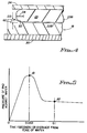
- a typical time for surface 22B to be compressed distance D3 is in the range of 0.001 to 0.003 seconds, typically about 0.002 seconds. Such a time could, however, be as low as about 0.0003 seconds.
- the distance of D3 presently equals about 70 microns.
- a 70 micron compression in 0.002 seconds roughly translates to a compression rate of about one inch per second. With velocity of movement or compression, the stiffness of a piece of material increases and the force required to compress the material increases. The graph in Fig. 5 reflects this phenomenon.
- point 60 is just at the outer edge of wafer 23 and is beginning to move underneath work surface 23B of wafer 23.
- point 60 on pad means 19 has moved a distance of D4 underneath wafer 23 and the resilient pads 21 and 22 have been compressed a distance indicated by arrows D3.
- the force of the pad means 19 acting against wafer 23 is, as we presently theorize it, at a maximum value indicated by point 61 in Fig. 5.
- Hysteresis is the tendency of a pad, after compressive pressure is released from the pad, not to elastically expand completely to its original shape.
- the pad includes resilient foam material 22 having a hydrostatic modulus much lower than the hydrostatic modulus of the "pad" formed by the mass of gas filled bubbles positioned beneath pad 22. Air, nitrogen or any other desired gas can be included in each elastic bubble 70. Bubbles 70 can be interconnected or be separate and stacked on one another. One or more bubbles 70 can be utilized. Each bubble 70 completely encapsulates the gas or other fluid contained in the bubble.
- a first elastic bubble 70 can be interconnected with a second adjacent elastic bubble 70 such that the interconnection permits gas to flow between the bubbles and such that neither bubble completely encapsulates the gas in the bubble. Consequently, when the first bubble was compressed, gas would tend to be forced from the first bubble into the second bubble.
- the gas in bubble 70 minimizes the increase in force which results with an increase in the velocity of compression and also minimizes the effects of hysteresis.
- bubbles 70 can be removed from cylindrical chamber 71, chamber 71 filed with a gas, and pad 22 sealingly slidably engaged with the upper portion of chamber 71 in the fashion of a piston such that when pad 22 is pressed downwardly in the direction of arrow X, the air in chamber 71 is compressed and forces the pad surface 22B into substantial conformance with the globally undulating wafer surface.
Abstract
Description
- This invention relates to planarizing apparatus.
- More particularly, the invention relates to apparatus for planarizing the macroscopically flat surface of a semiconductor wafer to expose microscopic features which have been formed in the semiconductor wafer and are below and covered by the macroscopically flat surface of the wafer.
- In a further respect, the invention relates to semiconductor planarizing apparatus of the type described which facilitates the removal at equal rates of areas of hard material and of soft material from the surface of a semiconductor wafer.
- Composite pads for polishing semiconductor materials are well known in the art. See, for example, U. S. Patent No. 3,504,457 to Jacobsen et al. The Jacobsen patent discloses a composite or multi-layer pad which includes a resilient foam polyurethane polishing layer or
film 23, an intermediate resilient Corfamlayer 20, and a chemically inert stiffernitrile rubber layer 35. In the Jacobsen composite polishing pad, the more resilient layers of the pad are adjacent the semiconductor while the stiffer nitrile rubber layer is further from the semiconductor which is being polished. While the resilient pads like the Jacobsen pad have long been utilized and accepted in polishing semiconductor materials, such conventional resilient pad structures do not appear to readily uniformly planarize a macroscopically or microscopically flat semiconductor surface which includes areas which are higher (or lower) than other areas of the semiconductor substrate or which includes areas which are softer than and abrade and flatten more quickly than other harder areas of the semiconductor surface. In particular, conventional pads tend to sit on and round the edges of a high area so the high area takes on the shape of a rounded mound. The planarization and flattening of the surface of a semiconductor material is particularly critical during the process of photolithography. During a typical photolithography process a metal film of aluminum, tungsten, polysilicon, etc. is deposited on a flat semiconductor wafer. A layer of photoresist is sprayed on or otherwise applied to the metal film. The photoresist is photoactive. A mask is placed over the photoresist layer and the layer and mask are exposed to light. The areas of photoresist which are not covered by the mask are exposed to the light and harden. The mask is removed. A chemical is utilized to remove the unexposed, unhardened areas of the photoresist. Another chemical is utilized to etch off the unprotected metal which is exposed when the unexposed photoresist is etched off. Still another chemical is then utilized to remove the hardened photoresist from the lines or strips of metal film which remain on the flat semiconductor wafer. After the hardened photoresist is removed, the metal lines or strips which remain on the flat semiconductor wafer typically have a width in the range of about 0.3 to 2.0 microns, preferably, in the range of 0.5 to 1.0 microns. The thickness or height of the metallic lines is also in the range of 0.3 to 2.0 microns, preferably 0.5 to 1.5 microns. A coating of silicon dioxide or other metal oxide or other insulating material is then deposited over the metal lines and remaining open areas of the flat semiconductor material. The depth or thickness of the metallic oxide coating is greater than the height of the metal lines, i.e., is greater than the 0.3 to 2.0 micron height of the metal lines. This metallic oxide is polished until the tops of the metal lines are "exposed". Such "exposing" of the metal lines consists of polishing away all the metal oxide on top of the metal lines or of polishing away most of the metal oxide so only a thin layer of metal oxide remains on the metal lines. The metal lines can have a hardness greater than that of the insulating coating which is intermediate the metal lines, in which case the insulating coating tends to be "scoured" out between the metal lines such that a flat planar surface is not formed during the interlayer dielectric planarization of the metal lines--insulator material. Alternately, the metal lines can have a hardness less than that of the insulating coating which is intermediate the metal lines, in which case the metal lines tend to be "scoured" out when the polishing process is continued after all of the insulating coating is removed from above the metal lines. - While a metal or metal-like material may be deposited on a semiconductor wafer, the primary objective in removing a material deposited on a semiconductor wafer is to planarize or flatten the surface of the wafer and is not making the surface of the wafer smoother. In contrast, the primary purpose of polishing a metal is typically to make the surface of the metal smooth. The distinction between polishing for the purpose of smoothness and removing material for the purpose of flatness is an important one and affects the characteristics of the planarizing apparatus selected. Polishing apparatus which is effective in producing a smooth surface may not be successful in producing the close tolerance flat or planar surfaces required in the production of semiconductor materials.
- Accordingly, it would be highly desirable to provide an improved apparatus and method for planarizing semiconductor materials, which apparatus and method would accurately planarize a semiconductor surface comprised of materials which have differing polishing characteristics.
- Therefore, it is a principal object of the invention to provide an improved apparatus and method for planarizing a material to produce a flat surface on the material.
- A further object of the invention is to provide an improved planarization method and apparatus which effectively flattens within close tolerances the surface of a semiconductor material containing compositions of differing hardness.
- Another object of the instant invention is to provide an improved composite planarization pad which includes layers of material having differing hydrostatic moduli.
- Still a further object of the invention is to provide an improved planarization pad which minimizes the effect of hysteresis on the elastic compression and expansion of the pad.
- These and other, further and more specific objects and advantages of the invention will be apparent to those skilled in the art from the following detailed description thereof, taken in conjunction with the drawings, in which:
- Fig. 1 is a side view illustrating a semiconductor material with an undulating microscopically flat surface and a portion of a composite polishing pad utilized to planarize the surface of the semiconductor material;
- Fig. 2 is a side section view of portions of the polishing pad and semiconductor material of Fig. 1 further illustrating construction details thereof;
- Fig. 3 is a side section view of a semiconductor material illustrating the median plane through the macroscopically or microscopically flat surface of the semiconductor material;
- Fig. 4 is a side section view illustrating the compression of the composite polishing pad of the invention as it moves underneath a wafer of semiconductor material;
- Fig. 5 is a graph representing the presence of a resilient polishing pad against a semiconductor material in relation to the time elapsed from when the pad first begins to move beneath the semiconductor material;
- Fig. 6 is a top view of the pad and wafer carrier of Figs. 1 and 4;
- Fig. 7 is a section view illustrating an alternate planarizing pad of the invention; and,
- Fig. 8 is a section view illustrating a planarization pad with three active layers.
- Briefly, in accordance with our invention, we provide improved apparatus for planarizing a piece of material. The piece of material includes a macroscopically flat subsurface; at least a pair of features each connected to the subsurface, each extending a substantially equal distance above the subsurface, and being spaced apart a distance of less than five hundred microns; and, a coat extending over and covering the features and the subsurface. The surface of the coating comprises a work surface which is macroscopically flat. The improved planarizing apparatus microscopically flattens the work surface to expose the pair of features and includes polishing pad means. The polishing pad means includes a base; a first layer of resilient material connected to the base and having an outer surface spaced apart from the base and having a hydrostatic modulus which is less than about 250 to 400 psi when a pressure in excess of about four psi is applied to the first layer of material; a second layer of resilient material connected to at least a portion of the outer surface, having a planarizing surface spaced apart from the outer surface, and including a slurry polishing media on the planarizing surface of the second layer. The improved planarizing apparatus also includes retaining means for holding the piece of material with the work surface disposed against the planarizing surface; and, motive power means for moving at least one of the pad means and the retaining means with respect to the other such that movement of the one of the pad means and the retaining means causes the slurry media and planarizing surface to contact and planarize the work surface.
- Turning now to the drawings, which depict the presently preferred embodiments of the invention for the purpose of illustrating the practice thereof and not by way of limitation of the scope of the invention, and in which like reference characters refer to corresponding elements throughout the several views, Fig. 1 illustrates a cylindrical piece of wafer or
semiconductor material 23 or other material mounted on acylindrical polishing head 24.Head 24 has acircular support surface 24A which receives the macroscopically flat circularplanar bottom surface 23A ofwafer 23. As used herein, the term "macroscopically flat" indicates that a surface appears flat to the human eye. The term "microscopically flat" indicates that a surface has a small undulation which ordinarily equals a 0.1 to 4.0 micron deviation from a median plane passing through the surface. For example, the distance D5 for the microscopicallyflat subsurface 23B in Fig. 1 is typically on the order of about two to three microns. As used herein, the term "microscopically flat" indicates a surface that has a deviation of 4.0 microns or less from a median plane passing through the surface. A macroscopically flat surface may or may not be microscopically flat. - The deviation of the work surface of a semiconductor wafer from the median plane of the wafer is further explained with reference to Fig. 3. In Fig. 3
semiconductor wafer 230 is mounted oncylindrical head 24. The circularplanar support surface 24A ofhead 24 receives the macroscopically flat circularplanar bottom surface 230A ofwafer 230. Theupper work surface 230B is macroscopically and microscopically flat and generally parallel tosurface 24A. The undulation ofsurface 230B in Fig. 3 (and ofsurface 23B in Fig. 1) is drawn greatly exaggerated. Dashedline 15 in Fig. 3 represents the median plane for surface 120B.Median plane 15 in Fig. 3 is, but need not be, generally parallel tosurface 24A and is perpendicular to the plane of the sheet of paper of the drawings.Median plane 15 intersectssurface 230B such that the sum of all distances to points underneathmedian plane 15 and of all distances to points abovemedian plane 15 is zero. The distance to points beneathplane 15 are treated as negative values while the distances to point above themedian plane 15 are treated as positive values. Therefore, in Fig. 3 the distance indicated by arrows G is a negative value while the distance indicated by the arrows F is a positive value. In actual practice, distances such as those indicated by arrows F and G in Fig. 3 are in the range of about 0.1 to 4.0 microns.Median plane 15 is perfectly flat. - Returning to Fig. 1, pad means 19 includes a
cylindrical metal base 20 with a circular planarupper surface 20A. The macroscopically flat planarbottom surface 21A ofresilient pad 21 is attached to surface 20A, typically with a layer of adhesive. Upper macroscopically planar surface 21B is attached to the lower macroscopicallyplanar surface 22A offlexible pad 22. Adhesive is ordinarily utilized to interconnectsurfaces 21B and 22A, although Figure 8 will show a further improvement. Theupper surface 22B ofresilient pad 22 is generally macroscopically planar and can be microscopically planar.Surfaces - Fig. 2 is a section view of the pad means 19 and
semiconductor wafer 23 of Fig. 1 further detailing construction details thereof. Thewafer 23 includes a macroscopicallyplanar subsurface 35.Features subsurface 35 and extend a substantially equal distance away fromsubsurface 35.Features 31 to 34 each represent a line or strip of metal or some other material formed onsubsurface 35 using the photolithography process earlier described.Features 31 to 34 each includes side surfaces which extend outwardly away fromsubsurface 35 to a relatively planar outer surface comprising the tip of eachfeature 31 to 34. The side surfaces of eachfeature 31 to 34 are generally perpendicular tosubsurface 35. The outer surface or tip of eachfeature 31 to 34 is generally parallel tosubsurface 35. An alternate method of forming features which are connected to and extend away fromsubsurface 35 is to formtrenches coating layer 30 extends over and covers features 31 to 34, 36, 38 and coverssubsurface 35. The high areas ofcoating 30 which "mound" or extend overfeatures 31 to 34 abrade at a different rate than the low areas ofcoating 30intermediate features coating layer 30 is greater than the distance which each feature 31 to 34 extends away fromsubsurface 35. Sincefeatures work surface 23B is at all points a greater distance fromsubsurface 35 than are the uppermost planar portions or tips offeatures 31 to 34. The shape and dimension of eachtrench feature 31 to 34. It is understood that features 31 to 34, 36, and 38 can be of any desired shape and dimension. The polishing apparatus of the invention is, however, particularly useful when it is necessary to planarizework surface 23B to remove a sufficient thickness ofcoating 30 to expose only the flat, planar tips or other outermost parts offeatures 31 to 34. In so removing a portion ofcoating 30, it is desired that the resulting surface of coating 30 be flat, i.e., be planarized. It is also desired that the side surfaces offeatures 31 to 34 not be exposed but remain covered bylayer 30. Accordingly,planarizing surface 22B does not conform to features 31 to 34 by extending over the side surfaces offeatures 31 to 34. It is, however, important that thesurface 22B of thematerial comprising pad 22 directly contact thework surface 23 or slurryintermediate pad 22 andsurface 23. For the purposes of discussion, the undulation insubsurface 35 and work surface 34B is, in Fig. 2, greatly exaggerated. - In Fig. 1, when the
resilient pads work surface 23B (or vice-versa), thepads surface 23B bypads compressed pads surface 23B, simply becausepads surface 23B at point A than at point B. Similarly, in Fig. 2, the forces F1 and F2 acting againstsurface 23B are greater than the forces F3 and F4 acting againstsurface 23B, again because the pad portions producing forces F1 and F2 are more greatly compressed than the pad portions producing forces F3 and F4. - Suitable materials for
layers layer 21 may utilize conventionally manufactured foam materials such as the neoprene foam used to make diver's wet-suits. All of these materials are easily bonded together by ordinary adhesives commonly known in the art. - In preparing pads of this invention, it was found that the adhesive layer between
surfaces layer 22 could be further optimized to improve performance on such structures. The existence of the non-resilient layer permits thepolishing layer 22 to have a greater volume compressibility and less likely to cause damage to fragile features of the work surface, while still yielding good planarization. Fig. 8 illustrates a pad of such construction whereinlayer 93 is the adhesive required for bonding the pad tobase 20;layer 21 is an elastic material containing at least 30% and preferably 40% - 70% of its volume composed of void volume;layer 91 is a thin film of essentially non-resilient, non-compressible material such as polyester, nylon, metal, epoxy, fiberglass reinforced epoxy, or the like which typically has a hardness of at least 90° Shore A; andlayer 22 is selected to have at least 25% and preferably more than 35% void volume. In the pad of Fig. 8,layer 22 must have a thickness of at least 5 mils and preferably 10 to 35 mils;layer 91 at least 3 mils and preferably 5 to 15 mils thickness;layer 21 may be almost any thickness greater than 15 mils, a thickness of 30 to 50 mils works well in most applications. In the construction of Fig. 8, bothlayers layer 21 must be at least 5% under a load of 10 psi., and for most applications a compressibility of 10% to 30% will be most suitable.Layer 22 which comes in contact with the workpiece sees very high localized compressive forces. It must have a volume compressibility of at least 5% under a load of 100 psi. - In Fig. 2,
surface 22B contacts and rotates overwork surface 23B. An aqueous suspension of silica, alumina or other abrasive (the "slurry") is onsurface 22B and gradually removes material from andplanarizes work surface 23B. The rotation ofsurface 22B with respect towork surface 23B is illustrated in Fig. 6. In Fig. 6circular surface 22B rotates in the direction of arrowW. Stationery head 24 presseswork surface 23B againstplanarizing surface 22B.Head 24 can, if desired, rotate or otherwise move with respect tosurface 22B. - The objective of planarizing pad means 19 is to produce a
surface 23B which is substantially microscopically flat or planar to within plus or minus 200 to 500 Angstroms Total Indicator Runout (T.I.R.) of a square portion ofsurface area 23B which is four millimeters by four millimeters, i.e., which has an area of sixteen square millimeters. A T.I.R. of 200 to 500 Angstroms means that there is a difference of 200 Angstroms between the lowest point and the highest point on the surface within the sixteen square millimeter area ofsurface 23B. A T.I.R. in the range of 200 to 500 Angstroms is generally equivalent to a plus or minus deviation of 100 to 250 Angstroms from the median plane of the sixteen square millimeter area. While the apparatus of the invention has produced a T.I.R. of 200 to 500 Angstroms in a sixteen square millimeter area, the apparatus is preferably used to produce a T.I.R. of 200 to 500 Angstroms in a square portion ofsurface area 23B which has an area of at least four square millimeters. It is desired to eventually achieve with the invention or with improved embodiments thereof a T.I.R. of 200 to 500 Angstroms over a surface area of 23B which is twenty millimeters by twenty millimeters, i.e., which has an area of 400 square millimeters. - Problems are encountered in
planarizing coating 30 becausefeatures 31 to 34 often have a different hardness or removal properties than thematerial comprising coating 30. If, for example, coating 30 abrades more readily thanfeatures intermediate features intermediate features - The planarization apparatus of the invention minimizes or prevents the scouring of softer material from the surface of a semiconductor material. For example, when the distance between
high features coating 30 is an insulative metal oxide or other material which is harder or softer than or is of the same hardness asfeatures features - An important distinction in the understanding of this invention is the distinction between hardness, resilience, stiffness, etc. on one hand and volume compressibility on the other. Although prior art has been concerned with properties of hardness, resilience, etc. in polishing pads, these terms are often used to reflect the material's resistance to bending distortion or ability to recover after such distortion, simply because the prior art is concerned with the conforming of a pad to irregularities in the work surface of a semiconductor and is not focusing on planarization. For example, a piece of solid, soft rubber may be said to be "not hard" or "stiff." These terms describe the ease of changing the shape of a pad (modulous of distortion) even though there is no change in the volume of the pad. In the present invention, layers 21 and 22 must manifest a change in volume, not just shape. "Compressibility" as used in this invention refers to change in volume as indicated by volumetric strain.
- In the practice of the invention, the
resilient layer 22 has a hydrostatic modulus, K, in the range of 400 to 5000 psi (assuming that the thickness of the layer is small compared to the diameter of the layer 22) per psi of compressive pressure when a compressive pressure in the range of four psi to twenty psi is applied to thelayer 22. For example, if a compressive force of four psi is applied tolayer 22, then the hydrostatic modulus, K, oflayer 22 is in the range of 1600 to 20,000 psi. If a compressive force of twenty psi is applied to layer 22 then the hydrostatic modulus, K, oflayer 22 is in the range of 8000 to 100,000 psi. Theresilient layer 21 has a hydrostatic modulus of greater than 100 psi per psi of the compressive pressure when a compressive force in the range of four psi to twenty psi is applied tolayer 21. The hydrostatic modulus oflayer 21 presently preferably is in the range of 100 to 250 psi per psi of compressive force when a compressive force in the range of four psi to twenty psi is applied to thelayer 21. For example, if a compressive pressure of ten psi is applied tolayer 21, then layer 21 has a hydrostatic modulus in the range of 1000 to 2500 psi. The hydrostatic modulus K measures the resistance to change in volume without changes in shape under a hydrostatic pressure P. The hydrostatic modulus K equals (Pv)/(Δv), where P is the hydrostatic pressure applied to the layer (assuming that the layer is initially under no pressure), and (Δv)/(v) is the volumetric strain. The low hydrostatic modulus oflayer 21permits layer 21 to elastically deform. The high hydrostatic modulus oflayer 22 helps to prevent scouring of soft material fromwork surface 23B, for instance, from betweenfeatures layer 22 promotes the bridging and planarizing bylayer 22 of areas such as the area intermediate features 31 and 32.Layer 22 effectively bridges areas which are spaced a distance apart, indicated by arrows E in Fig. 3, that is up to about 500 to 600 microns. Urethane foams and other types of foam or elastic materials can be utilized in the practice of the invention as long as the desired hydrostatic modulus values are obtained. - In arriving at the pad composition of the invention, it was important to recognize certain characteristics of the type of material removal being accomplished and of the materials utilized in the planarizing pad. First, the primary purpose of abrading the work surface of a
coating 30 is planarization. This contrasts to the primary purpose of smoothness common to many polishing operations. Second, the planarizing apparatus of the invention is designed to simultaneously contact all or most of the points on a macroscopically or microscopically flat surface of a piece of material to abrade and planarize the surface. This type of material removal is distinguishable from operations which polish a limited area of a piece of material and, accordingly, constitute a point contact type of material removal. Third, a critical property of the composite planarizing pad of the invention is the hydrostatic modulus, K, of the resilient layers of material utilized in the pad. In Fig. 6, the portion ofpad 22 following path P1 is compressed underwafer 23 for a longer period of time during each rotation ofpad 22 than is portion ofpad 22 which follows path P2. Regardless, however, of whether thepad 22 follows path P1 or P2, the time required to compresspads 21 and 22 (See also Figs. 2 and 3) beneathwafer 23 is generally about the same. This is more specifically illustrated in Fig. 4, where the time required to compress the flexible pads comprising pad means 19 is indicated by the time required forpads surface 22B contacts therounded edge 50 ofwafer 23 and moves the distance indicated by arrows D4 underwafer 23, the surface of pad means 10 is compressed a distance indicated by arrows D3. A typical time forsurface 22B to be compressed distance D3 is in the range of 0.001 to 0.003 seconds, typically about 0.002 seconds. Such a time could, however, be as low as about 0.0003 seconds. The distance of D3 presently equals about 70 microns. A 70 micron compression in 0.002 seconds roughly translates to a compression rate of about one inch per second. With velocity of movement or compression, the stiffness of a piece of material increases and the force required to compress the material increases. The graph in Fig. 5 reflects this phenomenon. At a time equal to zero seconds in Fig. 5,point 60 is just at the outer edge ofwafer 23 and is beginning to move underneathwork surface 23B ofwafer 23. At a time equal to 0.002 seconds in Fig. 5,point 60 on pad means 19 has moved a distance of D4 underneathwafer 23 and theresilient pads time point 60 has moved distance D4 underwafer 23, the force of the pad means 19 acting againstwafer 23 is, as we presently theorize it, at a maximum value indicated bypoint 61 in Fig. 5. Aspoint 60 on pad means 19 continues to move beneathwafer 23, the force generated by thecompressed pads wafer 23 gradually reduces until afterpoint 60 of the pad means 19 has been underwafer 23 for 0.1 seconds the force generated by pad means 19 againstwafer 23 atpoint 60 is indicated bypoint 62 in Fig. 5. This increase in the force generated by pad means 19 againstwafer 23 with an increase in the velocity of compression ofpads pad 21 to quickly react and conform to undulations in the workingsurface 23B ofwafer 23 while maintaining a more uniform pressure against thewafer 23. - Another problem associated with elastic pads fabricated from foam or other materials is hysteresis. Hysteresis is the tendency of a pad, after compressive pressure is released from the pad, not to elastically expand completely to its original shape.
- In order to minimize the problem of hysteresis and to minimize the increase in force which occurs with an increase in the velocity of compression of an elastic pad material, we have discovered the composite pad shown in Fig. 7. The pad includes
resilient foam material 22 having a hydrostatic modulus much lower than the hydrostatic modulus of the "pad" formed by the mass of gas filled bubbles positioned beneathpad 22. Air, nitrogen or any other desired gas can be included in eachelastic bubble 70.Bubbles 70 can be interconnected or be separate and stacked on one another. One ormore bubbles 70 can be utilized. Eachbubble 70 completely encapsulates the gas or other fluid contained in the bubble. If desired, a firstelastic bubble 70 can be interconnected with a second adjacentelastic bubble 70 such that the interconnection permits gas to flow between the bubbles and such that neither bubble completely encapsulates the gas in the bubble. Consequently, when the first bubble was compressed, gas would tend to be forced from the first bubble into the second bubble. The gas inbubble 70 minimizes the increase in force which results with an increase in the velocity of compression and also minimizes the effects of hysteresis. As would be appreciated by those of skill in the art, bubbles 70 can be removed fromcylindrical chamber 71,chamber 71 filed with a gas, and pad 22 sealingly slidably engaged with the upper portion ofchamber 71 in the fashion of a piston such that whenpad 22 is pressed downwardly in the direction of arrow X, the air inchamber 71 is compressed and forces thepad surface 22B into substantial conformance with the globally undulating wafer surface. - Having described our invention in such terms as to enable those skilled in the art to understand and practice it, and having identified the presently preferred embodiments thereof, we Claim:
Claims (12)
- Apparatus for planarizing a piece of material including
a macroscopically flat subsurface,
at least a pair of features
each connected to said subsurface,
each having an outer surface spaced away from said subsurface,
each extending a substantially equal distance away from said subsurface,
being spaced apart a distance of less than five hundred microns,
a coating extending over and covering said features and said subsurface, the outer surface of said coating comprising a work surface which is macroscopically flat,
said apparatus including(a) planarizing pad means including(i) a base,(ii) a first layer of resilient material connected to said base and having an outer surface spaced apart from said base and having a hydrostatic modulus which is less than 250 psi per psi of compressive pressure when a selected compressive pressure in the range of about four psi to twenty psi is applied to said first layer,(iii) a second layer of resilient material connected to at least a portion of said outer surface, having a planarizing surface spaced apart from said outer surface to contact and abrade said coating to expose said upper surface, and having a hydrostatic modulus greater than the hydrostatic modulus of said first layer when said selected compressive pressure is applied to said second layer, and(iv) a liquid slurry polishing media on said planarizing surface of said second layer;(b) retaining means for holding said piece of material with said work surface disposed against and contacting at least one of the pair consisting of (i) said planarizing surface, and, (ii) said slurry media; and,(c) motive power means for moving at least one of said planarizing pad means and said retaining means with respect to the other of said pad means and said retaining means such that movement of said one of said pad means and said holding means causes said slurry and said planarizing surface to contact and abrade said work surface;said planarizing surface microscopically planarizing at least said work surface to expose said outer surfaces of said features such that
said work surface and said outer surfaces are generally microscopically flat and co-planar,
said outer surfaces each terminate at and abut said work surface. - The apparatus of Claim 1 wherein(a) each of said features includes at least one side surface extending outwardly from said subsurface and terminating at said outer surface;(b) said coating(i) before said subsurface is planarized with said pad means, extends over and covers said side surfaces,(ii) after said subsurface is planarized to exposes said outer surfaces, extends over and covers said side surfaces, and(iii) has a minimum thickness greater than said distance which said features extend away from said subsurface.
- The apparatus of Claim 2 wherein said distance which said features extend away from said subsurface is in the range of 0.3 to 2.0 microns.
- The apparatus of Claim 3 wherein said material is a semiconductor material and said features each have a width in the range of 0.3 to 2.0 microns.
- A polishing pad for use with a planarization apparatus, said pad comprising(a) a resilient base material having a hydrostatic modulus which is less than about 250 psi per psi of compressive pressure when a selected compressive pressure in the range of about four psi to twenty psi is applied to said first layer of material; and,(b) a second planarizing layer having a hydrostatic modulus greater than about 400 psi per psi of compressive pressure when said selected compressive pressure is applied to said second layer of material;said pad being capable of being mounted on said planarizing apparatus to act alone or in conjunction with a slurry to planarize the work surface of a workpiece.
- The polishing pad of Claim 5 wherein said second layer is comprised of a material having a planarizing surface which contacts at least one of the pair comprising(a) said work surface, and(b) when said pad is used in conjunction with said slurry, said slurry.
- Apparatus for planarizing a work surface of a piece of material, said work surface being macroscopically flat and microscopically flat such that said work surface deviates at all points from the median plane passing through said work surface by an amount less than about four microns,
said apparatus including(a) planarizing pad means including(i) a base,(ii) a first layer of resilient material connected to said base and having an outer surface spaced apart from said base and having a hydrostatic modulus which is less than 250 psi per psi of compressive pressure when a selected compressive pressure in excess of about four psi is applied to said first layer of material,(iii) a second layer of resilient material connected to at least a portion of said outer surface, having a planarizing surface spaced apart from said outer surface, and having a hydrostatic modulus greater than the hydrostatic modulus of said first layer when said selected compressive pressure is applied to said second layer of material, and(iv) a slurry media on said planarizing surface of said second layer;(b) retaining means for holding said piece of material with said work surface disposed against and contacting at least one of the pair consisting of(i) said planarizing surface, and,(ii) said slurry media;(c) motive power means for moving at least one of said pad means and said retaining means with respect to the other such that movement of said one of said pad means and said holding means causes said slurry and said planarizing surface to contact and abrade said work surface. - The apparatus of Claim 7, wherein the total combined area of said first and second areas is less than sixteen square millimeters.
- A polishing pad for use with a planarization apparatus comprising(a) a resilient base material being at least .015" thick and having at least 30% of its volume composed of voids such that the base material is volume compressible and will compress at least 5% under a load of 10 psi,(b) an intermediate layer at least .003" thick which is essentially volume incompressible,(c) a top planarizing layer at least .005" thick, having at least 25% of its volume composed of voids such that the planarizing layer is volume compressible and will compress at least 5% under a load of 100 psi.,said polishing pad being capable of being mounted on a suitable apparatus for planarization and by acting alone or in conjunction with a slurry to produce a planar surface on a workpiece.
- The polishing pad of claim 8 wherein at least some of the voids in the top planarizing layer are formed by the incorporation of micro-spheres containing gas.
- The polishing pad of claim 9 wherein at least some of the voids in the resilient base layer are formed by the incorporation of micro-spheres containing gas.
- A polishing pad for use with a planarization apparatus comprising(a) a resilient base material being at least .015" thick and having at least 30% of its volume composed of voids such that the base material is volume compressible and will compress at least 5% under a load of 10 psi; and,(b) a top planarizing layer at least .005" thick, having at least 25% of its volume composed of voids such that the planarizing layer is volume compressible and will compress at least 5% under a load of 100 psi.;said polishing pad being capable of being mounted on a suitable apparatus for planarization and by acting alone or in conjunction with a slurry to produce a planar surface on a workpiece.
Applications Claiming Priority (2)
| Application Number | Priority Date | Filing Date | Title |
|---|---|---|---|
| US07/829,736 US5257478A (en) | 1990-03-22 | 1992-01-31 | Apparatus for interlayer planarization of semiconductor material |
| US829736 | 1992-01-31 |
Publications (3)
| Publication Number | Publication Date |
|---|---|
| EP0555660A2 true EP0555660A2 (en) | 1993-08-18 |
| EP0555660A3 EP0555660A3 (en) | 1994-03-23 |
| EP0555660B1 EP0555660B1 (en) | 1997-03-19 |
Family
ID=25255407
Family Applications (1)
| Application Number | Title | Priority Date | Filing Date |
|---|---|---|---|
| EP93100667A Expired - Lifetime EP0555660B1 (en) | 1992-01-31 | 1993-01-18 | Apparatus for interlayer planarization of semiconductor material |
Country Status (7)
| Country | Link |
|---|---|
| US (1) | US5257478A (en) |
| EP (1) | EP0555660B1 (en) |
| JP (1) | JP3455556B2 (en) |
| KR (1) | KR100265660B1 (en) |
| CN (1) | CN1076152A (en) |
| DE (1) | DE69308915T2 (en) |
| TW (1) | TW222033B (en) |
Cited By (8)
| Publication number | Priority date | Publication date | Assignee | Title |
|---|---|---|---|---|
| EP0658401A1 (en) * | 1993-12-14 | 1995-06-21 | Shin-Etsu Handotai Company Limited | Polishing member and wafer polishing apparatus |
| EP0845328A2 (en) * | 1996-11-29 | 1998-06-03 | Sumitomo Metal Industries, Ltd. | Polishing pad and apparatus for polishing a semiconductor wafer |
| WO1998047662A1 (en) * | 1997-04-18 | 1998-10-29 | Cabot Corporation | Polishing pad for a semiconductor substrate |
| EP0919336A2 (en) * | 1997-11-25 | 1999-06-02 | Speedfam Co., Ltd. | Surface polishing pad |
| WO2000027589A1 (en) * | 1998-11-09 | 2000-05-18 | Toray Industries, Inc. | Polishing pad and polishing device |
| US6117000A (en) * | 1998-07-10 | 2000-09-12 | Cabot Corporation | Polishing pad for a semiconductor substrate |
| WO2001078125A1 (en) * | 2000-04-12 | 2001-10-18 | Shin-Etsu Handotai Co.,Ltd. | Method for producing semiconductor wafer and semiconductor wafer |
| EP1295680A2 (en) * | 2001-09-25 | 2003-03-26 | JSR Corporation | Polishing pad for semiconductor wafer |
Families Citing this family (150)
| Publication number | Priority date | Publication date | Assignee | Title |
|---|---|---|---|---|
| JPH0697132A (en) * | 1992-07-10 | 1994-04-08 | Lsi Logic Corp | Mechanochemical polishing apparatus of semiconductor wafer, mounting method of semiconductor-wafer polishing pad to platen of above apparatus and polishing composite pad of above apparatus |
| US7037403B1 (en) * | 1992-12-28 | 2006-05-02 | Applied Materials Inc. | In-situ real-time monitoring technique and apparatus for detection of thin films during chemical/mechanical polishing planarization |
| US6614529B1 (en) * | 1992-12-28 | 2003-09-02 | Applied Materials, Inc. | In-situ real-time monitoring technique and apparatus for endpoint detection of thin films during chemical/mechanical polishing planarization |
| US5489233A (en) * | 1994-04-08 | 1996-02-06 | Rodel, Inc. | Polishing pads and methods for their use |
| US5534106A (en) * | 1994-07-26 | 1996-07-09 | Kabushiki Kaisha Toshiba | Apparatus for processing semiconductor wafers |
| US5783497A (en) * | 1994-08-02 | 1998-07-21 | Sematech, Inc. | Forced-flow wafer polisher |
| US5562530A (en) * | 1994-08-02 | 1996-10-08 | Sematech, Inc. | Pulsed-force chemical mechanical polishing |
| US5607341A (en) | 1994-08-08 | 1997-03-04 | Leach; Michael A. | Method and structure for polishing a wafer during manufacture of integrated circuits |
| US5679610A (en) * | 1994-12-15 | 1997-10-21 | Kabushiki Kaisha Toshiba | Method of planarizing a semiconductor workpiece surface |
| US5893796A (en) | 1995-03-28 | 1999-04-13 | Applied Materials, Inc. | Forming a transparent window in a polishing pad for a chemical mechanical polishing apparatus |
| DE69618698T2 (en) | 1995-03-28 | 2002-08-14 | Applied Materials Inc | Method and device for in-situ control and determination of the end of chemical-mechanical leveling processes |
| US6676717B1 (en) | 1995-03-28 | 2004-01-13 | Applied Materials Inc | Apparatus and method for in-situ endpoint detection for chemical mechanical polishing operations |
| US6876454B1 (en) * | 1995-03-28 | 2005-04-05 | Applied Materials, Inc. | Apparatus and method for in-situ endpoint detection for chemical mechanical polishing operations |
| US6537133B1 (en) * | 1995-03-28 | 2003-03-25 | Applied Materials, Inc. | Method for in-situ endpoint detection for chemical mechanical polishing operations |
| US5945347A (en) | 1995-06-02 | 1999-08-31 | Micron Technology, Inc. | Apparatus and method for polishing a semiconductor wafer in an overhanging position |
| JP3329644B2 (en) * | 1995-07-21 | 2002-09-30 | 株式会社東芝 | Polishing pad, polishing apparatus and polishing method |
| TW334379B (en) * | 1995-08-24 | 1998-06-21 | Matsushita Electric Ind Co Ltd | Compression mechanism for grinding machine of semiconductor substrate |
| US5899799A (en) * | 1996-01-19 | 1999-05-04 | Micron Display Technology, Inc. | Method and system to increase delivery of slurry to the surface of large substrates during polishing operations |
| US6135856A (en) * | 1996-01-19 | 2000-10-24 | Micron Technology, Inc. | Apparatus and method for semiconductor planarization |
| US6081959A (en) * | 1996-07-01 | 2000-07-04 | Umbrell; Richard | Buffer centering system |
| US5692950A (en) * | 1996-08-08 | 1997-12-02 | Minnesota Mining And Manufacturing Company | Abrasive construction for semiconductor wafer modification |
| US5785584A (en) * | 1996-08-30 | 1998-07-28 | International Business Machines Corporation | Planarizing apparatus with deflectable polishing pad |
| JP2738392B1 (en) * | 1996-11-05 | 1998-04-08 | 日本電気株式会社 | Polishing apparatus and polishing method for semiconductor device |
| US6379221B1 (en) | 1996-12-31 | 2002-04-30 | Applied Materials, Inc. | Method and apparatus for automatically changing a polishing pad in a chemical mechanical polishing system |
| US6328642B1 (en) | 1997-02-14 | 2001-12-11 | Lam Research Corporation | Integrated pad and belt for chemical mechanical polishing |
| US5968851A (en) * | 1997-03-19 | 1999-10-19 | Cypress Semiconductor Corp. | Controlled isotropic etch process and method of forming an opening in a dielectric layer |
| US6425812B1 (en) | 1997-04-08 | 2002-07-30 | Lam Research Corporation | Polishing head for chemical mechanical polishing using linear planarization technology |
| US6244946B1 (en) | 1997-04-08 | 2001-06-12 | Lam Research Corporation | Polishing head with removable subcarrier |
| US6126532A (en) * | 1997-04-18 | 2000-10-03 | Cabot Corporation | Polishing pads for a semiconductor substrate |
| US5885135A (en) * | 1997-04-23 | 1999-03-23 | International Business Machines Corporation | CMP wafer carrier for preferential polishing of a wafer |
| US8092707B2 (en) | 1997-04-30 | 2012-01-10 | 3M Innovative Properties Company | Compositions and methods for modifying a surface suited for semiconductor fabrication |
| US6108091A (en) | 1997-05-28 | 2000-08-22 | Lam Research Corporation | Method and apparatus for in-situ monitoring of thickness during chemical-mechanical polishing |
| TW375550B (en) * | 1997-06-19 | 1999-12-01 | Komatsu Denshi Kinzoku Kk | Polishing apparatus for semiconductor wafer |
| US6736714B2 (en) | 1997-07-30 | 2004-05-18 | Praxair S.T. Technology, Inc. | Polishing silicon wafers |
| US5913713A (en) * | 1997-07-31 | 1999-06-22 | International Business Machines Corporation | CMP polishing pad backside modifications for advantageous polishing results |
| US6121143A (en) * | 1997-09-19 | 2000-09-19 | 3M Innovative Properties Company | Abrasive articles comprising a fluorochemical agent for wafer surface modification |
| US6234883B1 (en) | 1997-10-01 | 2001-05-22 | Lsi Logic Corporation | Method and apparatus for concurrent pad conditioning and wafer buff in chemical mechanical polishing |
| US6336845B1 (en) | 1997-11-12 | 2002-01-08 | Lam Research Corporation | Method and apparatus for polishing semiconductor wafers |
| US6096230A (en) * | 1997-12-29 | 2000-08-01 | Intel Corporation | Method of planarizing by polishing a structure which is formed to promote planarization |
| JP3618541B2 (en) * | 1998-03-23 | 2005-02-09 | 信越半導体株式会社 | Polishing cloth, polishing cloth processing method and polishing method |
| WO1999048645A1 (en) * | 1998-03-23 | 1999-09-30 | Speedfam-Ipec Corporation | Backing pad for workpiece carrier |
| US6298518B1 (en) | 1998-04-14 | 2001-10-09 | Richard T. Umbrell | Heat dissipating buffing pad |
| US6105197A (en) * | 1998-04-14 | 2000-08-22 | Umbrell; Richard T. | Centering system for buffing pad |
| US7718102B2 (en) * | 1998-06-02 | 2010-05-18 | Praxair S.T. Technology, Inc. | Froth and method of producing froth |
| US6514301B1 (en) | 1998-06-02 | 2003-02-04 | Peripheral Products Inc. | Foam semiconductor polishing belts and pads |
| US6315857B1 (en) | 1998-07-10 | 2001-11-13 | Mosel Vitelic, Inc. | Polishing pad shaping and patterning |
| US6126512A (en) * | 1998-07-10 | 2000-10-03 | Aplex Inc. | Robust belt tracking and control system for hostile environment |
| US6439967B2 (en) * | 1998-09-01 | 2002-08-27 | Micron Technology, Inc. | Microelectronic substrate assembly planarizing machines and methods of mechanical and chemical-mechanical planarization of microelectronic substrate assemblies |
| US6254463B1 (en) | 1998-10-09 | 2001-07-03 | International Business Machines Corporation | Chemical planar head dampening system |
| US6716085B2 (en) | 2001-12-28 | 2004-04-06 | Applied Materials Inc. | Polishing pad with transparent window |
| US6190234B1 (en) * | 1999-01-25 | 2001-02-20 | Applied Materials, Inc. | Endpoint detection with light beams of different wavelengths |
| US6994607B2 (en) * | 2001-12-28 | 2006-02-07 | Applied Materials, Inc. | Polishing pad with window |
| US6179709B1 (en) * | 1999-02-04 | 2001-01-30 | Applied Materials, Inc. | In-situ monitoring of linear substrate polishing operations |
| US6238592B1 (en) | 1999-03-10 | 2001-05-29 | 3M Innovative Properties Company | Working liquids and methods for modifying structured wafers suited for semiconductor fabrication |
| US20040072518A1 (en) * | 1999-04-02 | 2004-04-15 | Applied Materials, Inc. | Platen with patterned surface for chemical mechanical polishing |
| US6217426B1 (en) | 1999-04-06 | 2001-04-17 | Applied Materials, Inc. | CMP polishing pad |
| KR20010020807A (en) | 1999-05-03 | 2001-03-15 | 조셉 제이. 스위니 | Pre-conditioning fixed abrasive articles |
| US6406363B1 (en) | 1999-08-31 | 2002-06-18 | Lam Research Corporation | Unsupported chemical mechanical polishing belt |
| US6524164B1 (en) | 1999-09-14 | 2003-02-25 | Applied Materials, Inc. | Polishing pad with transparent window having reduced window leakage for a chemical mechanical polishing apparatus |
| US6299516B1 (en) | 1999-09-28 | 2001-10-09 | Applied Materials, Inc. | Substrate polishing article |
| US6431959B1 (en) | 1999-12-20 | 2002-08-13 | Lam Research Corporation | System and method of defect optimization for chemical mechanical planarization of polysilicon |
| US6533645B2 (en) | 2000-01-18 | 2003-03-18 | Applied Materials, Inc. | Substrate polishing article |
| US6623341B2 (en) | 2000-01-18 | 2003-09-23 | Applied Materials, Inc. | Substrate polishing apparatus |
| US6607428B2 (en) | 2000-01-18 | 2003-08-19 | Applied Materials, Inc. | Material for use in carrier and polishing pads |
| US7125477B2 (en) | 2000-02-17 | 2006-10-24 | Applied Materials, Inc. | Contacts for electrochemical processing |
| US7670468B2 (en) | 2000-02-17 | 2010-03-02 | Applied Materials, Inc. | Contact assembly and method for electrochemical mechanical processing |
| US7303462B2 (en) | 2000-02-17 | 2007-12-04 | Applied Materials, Inc. | Edge bead removal by an electro polishing process |
| US6979248B2 (en) | 2002-05-07 | 2005-12-27 | Applied Materials, Inc. | Conductive polishing article for electrochemical mechanical polishing |
| US7303662B2 (en) | 2000-02-17 | 2007-12-04 | Applied Materials, Inc. | Contacts for electrochemical processing |
| US6991528B2 (en) | 2000-02-17 | 2006-01-31 | Applied Materials, Inc. | Conductive polishing article for electrochemical mechanical polishing |
| US6962524B2 (en) * | 2000-02-17 | 2005-11-08 | Applied Materials, Inc. | Conductive polishing article for electrochemical mechanical polishing |
| US7678245B2 (en) | 2000-02-17 | 2010-03-16 | Applied Materials, Inc. | Method and apparatus for electrochemical mechanical processing |
| US7077721B2 (en) | 2000-02-17 | 2006-07-18 | Applied Materials, Inc. | Pad assembly for electrochemical mechanical processing |
| US7066800B2 (en) | 2000-02-17 | 2006-06-27 | Applied Materials Inc. | Conductive polishing article for electrochemical mechanical polishing |
| US6666756B1 (en) | 2000-03-31 | 2003-12-23 | Lam Research Corporation | Wafer carrier head assembly |
| US6616801B1 (en) | 2000-03-31 | 2003-09-09 | Lam Research Corporation | Method and apparatus for fixed-abrasive substrate manufacturing and wafer polishing in a single process path |
| US6267659B1 (en) * | 2000-05-04 | 2001-07-31 | International Business Machines Corporation | Stacked polish pad |
| US8485862B2 (en) | 2000-05-19 | 2013-07-16 | Applied Materials, Inc. | Polishing pad for endpoint detection and related methods |
| US7374477B2 (en) * | 2002-02-06 | 2008-05-20 | Applied Materials, Inc. | Polishing pads useful for endpoint detection in chemical mechanical polishing |
| US6495464B1 (en) | 2000-06-30 | 2002-12-17 | Lam Research Corporation | Method and apparatus for fixed abrasive substrate preparation and use in a cluster CMP tool |
| JP4916638B2 (en) | 2000-06-30 | 2012-04-18 | ローム アンド ハース エレクトロニック マテリアルズ シーエムピー ホウルディングス インコーポレイテッド | Base pad for polishing pad |
| US6666751B1 (en) * | 2000-07-17 | 2003-12-23 | Micron Technology, Inc. | Deformable pad for chemical mechanical polishing |
| CN1224499C (en) * | 2000-12-01 | 2005-10-26 | 东洋橡膠工业株式会社 | Polishing pad, method of mfg. polishing pad, and cushion layer polishing pad |
| US6896776B2 (en) | 2000-12-18 | 2005-05-24 | Applied Materials Inc. | Method and apparatus for electro-chemical processing |
| US6609961B2 (en) | 2001-01-09 | 2003-08-26 | Lam Research Corporation | Chemical mechanical planarization belt assembly and method of assembly |
| US6544107B2 (en) | 2001-02-16 | 2003-04-08 | Agere Systems Inc. | Composite polishing pads for chemical-mechanical polishing |
| US6863774B2 (en) * | 2001-03-08 | 2005-03-08 | Raytech Innovative Solutions, Inc. | Polishing pad for use in chemical-mechanical planarization of semiconductor wafers and method of making same |
| US7137879B2 (en) | 2001-04-24 | 2006-11-21 | Applied Materials, Inc. | Conductive polishing article for electrochemical mechanical polishing |
| US7097549B2 (en) * | 2001-12-20 | 2006-08-29 | Ppg Industries Ohio, Inc. | Polishing pad |
| US7037184B2 (en) * | 2003-01-22 | 2006-05-02 | Raytech Innovation Solutions, Llc | Polishing pad for use in chemical-mechanical planarization of semiconductor wafers and method of making same |
| US6852020B2 (en) * | 2003-01-22 | 2005-02-08 | Raytech Innovative Solutions, Inc. | Polishing pad for use in chemical—mechanical planarization of semiconductor wafers and method of making same |
| US20030194959A1 (en) * | 2002-04-15 | 2003-10-16 | Cabot Microelectronics Corporation | Sintered polishing pad with regions of contrasting density |
| US7025668B2 (en) * | 2002-06-18 | 2006-04-11 | Raytech Innovative Solutions, Llc | Gradient polishing pad made from paper-making fibers for use in chemical/mechanical planarization of wafers |
| KR100465649B1 (en) * | 2002-09-17 | 2005-01-13 | 한국포리올 주식회사 | Integral polishing pad and manufacturing method thereof |
| US20070010169A1 (en) * | 2002-09-25 | 2007-01-11 | Ppg Industries Ohio, Inc. | Polishing pad with window for planarization |
| CN100417493C (en) * | 2002-09-25 | 2008-09-10 | Ppg工业俄亥俄公司 | Polishing pad with window for planarization |
| JP2004160573A (en) * | 2002-11-11 | 2004-06-10 | Ebara Corp | Polishing device |
| TW592894B (en) * | 2002-11-19 | 2004-06-21 | Iv Technologies Co Ltd | Method of fabricating a polishing pad |
| US7141155B2 (en) | 2003-02-18 | 2006-11-28 | Parker-Hannifin Corporation | Polishing article for electro-chemical mechanical polishing |
| US7435161B2 (en) * | 2003-06-17 | 2008-10-14 | Cabot Microelectronics Corporation | Multi-layer polishing pad material for CMP |
| US6998166B2 (en) * | 2003-06-17 | 2006-02-14 | Cabot Microelectronics Corporation | Polishing pad with oriented pore structure |
| US6884156B2 (en) | 2003-06-17 | 2005-04-26 | Cabot Microelectronics Corporation | Multi-layer polishing pad material for CMP |
| US7264536B2 (en) * | 2003-09-23 | 2007-09-04 | Applied Materials, Inc. | Polishing pad with window |
| US7101275B2 (en) * | 2003-09-26 | 2006-09-05 | Rohm And Haas Electronic Materials Cmp Holdings, Inc. | Resilient polishing pad for chemical mechanical polishing |
| US7654885B2 (en) * | 2003-10-03 | 2010-02-02 | Applied Materials, Inc. | Multi-layer polishing pad |
| US20050173259A1 (en) * | 2004-02-06 | 2005-08-11 | Applied Materials, Inc. | Endpoint system for electro-chemical mechanical polishing |
| US8066552B2 (en) | 2003-10-03 | 2011-11-29 | Applied Materials, Inc. | Multi-layer polishing pad for low-pressure polishing |
| WO2005035194A2 (en) * | 2003-10-09 | 2005-04-21 | Thomas West, Inc. | Stacked pad and method of use |
| US7186651B2 (en) * | 2003-10-30 | 2007-03-06 | Texas Instruments Incorporated | Chemical mechanical polishing method and apparatus |
| US7186164B2 (en) | 2003-12-03 | 2007-03-06 | Applied Materials, Inc. | Processing pad assembly with zone control |
| JP3754436B2 (en) * | 2004-02-23 | 2006-03-15 | 東洋ゴム工業株式会社 | Polishing pad and semiconductor device manufacturing method using the same |
| TWI293266B (en) * | 2004-05-05 | 2008-02-11 | Iv Technologies Co Ltd | A single-layer polishing pad and a method of producing the same |
| US7198549B2 (en) * | 2004-06-16 | 2007-04-03 | Cabot Microelectronics Corporation | Continuous contour polishing of a multi-material surface |
| TWI254354B (en) * | 2004-06-29 | 2006-05-01 | Iv Technologies Co Ltd | An inlaid polishing pad and a method of producing the same |
| US7189156B2 (en) * | 2004-08-25 | 2007-03-13 | Jh Rhodes Company, Inc. | Stacked polyurethane polishing pad and method of producing the same |
| US8075372B2 (en) * | 2004-09-01 | 2011-12-13 | Cabot Microelectronics Corporation | Polishing pad with microporous regions |
| US7520968B2 (en) | 2004-10-05 | 2009-04-21 | Applied Materials, Inc. | Conductive pad design modification for better wafer-pad contact |
| US20060089095A1 (en) | 2004-10-27 | 2006-04-27 | Swisher Robert G | Polyurethane urea polishing pad |
| US7182677B2 (en) * | 2005-01-14 | 2007-02-27 | Applied Materials, Inc. | Chemical mechanical polishing pad for controlling polishing slurry distribution |
| US7427340B2 (en) | 2005-04-08 | 2008-09-23 | Applied Materials, Inc. | Conductive pad |
| US20070049169A1 (en) * | 2005-08-02 | 2007-03-01 | Vaidya Neha P | Nonwoven polishing pads for chemical mechanical polishing |
| US7226345B1 (en) | 2005-12-09 | 2007-06-05 | The Regents Of The University Of California | CMP pad with designed surface features |
| CN101244535B (en) * | 2006-02-15 | 2012-06-13 | 应用材料公司 | Polishing article |
| US20080274674A1 (en) * | 2007-05-03 | 2008-11-06 | Cabot Microelectronics Corporation | Stacked polishing pad for high temperature applications |
| JP2011507720A (en) * | 2007-12-31 | 2011-03-10 | イノパッド,インコーポレイテッド | Chemical mechanical planarization pad |
| CN102089122A (en) * | 2008-05-15 | 2011-06-08 | 3M创新有限公司 | Polishing pad with endpoint window and systems and method using the same |
| TWI409137B (en) * | 2008-06-19 | 2013-09-21 | Bestac Advanced Material Co Ltd | Polishing pad and the method of forming micro-structure thereof |
| KR20110019442A (en) * | 2008-06-26 | 2011-02-25 | 쓰리엠 이노베이티브 프로퍼티즈 캄파니 | Polishing pad with porous elements and method of making and using the same |
| US7645186B1 (en) * | 2008-07-18 | 2010-01-12 | Rohm And Haas Electronic Materials Cmp Holdings, Inc. | Chemical mechanical polishing pad manufacturing assembly |
| JP5450622B2 (en) * | 2008-07-18 | 2014-03-26 | スリーエム イノベイティブ プロパティズ カンパニー | Polishing pad with a floating element, method for producing and using the same |
| US7820005B2 (en) * | 2008-07-18 | 2010-10-26 | Rohm And Haas Electronic Materials Cmp Holdings, Inc. | Multilayer chemical mechanical polishing pad manufacturing process |
| TWM352127U (en) * | 2008-08-29 | 2009-03-01 | Bestac Advanced Material Co Ltd | Polishing pad |
| TWM352126U (en) * | 2008-10-23 | 2009-03-01 | Bestac Advanced Material Co Ltd | Polishing pad |
| KR20120125612A (en) | 2009-12-30 | 2012-11-16 | 쓰리엠 이노베이티브 프로퍼티즈 컴파니 | Polishing pads including phase-separated polymer blend and method of making and using the same |
| TWI510328B (en) * | 2010-05-03 | 2015-12-01 | Iv Technologies Co Ltd | Base layer, polishing pad including the same and polishing method |
| EP2643864A2 (en) | 2010-11-22 | 2013-10-02 | 3M Innovative Properties Company | Assembly and electronic devices including the same |
| US9067299B2 (en) | 2012-04-25 | 2015-06-30 | Applied Materials, Inc. | Printed chemical mechanical polishing pad |
| JP5789634B2 (en) * | 2012-05-14 | 2015-10-07 | 株式会社荏原製作所 | Polishing pad for polishing a workpiece, chemical mechanical polishing apparatus, and method for polishing a workpiece using the chemical mechanical polishing apparatus |
| JP6016301B2 (en) | 2013-02-13 | 2016-10-26 | 昭和電工株式会社 | Surface processing method of single crystal SiC substrate, manufacturing method thereof, and grinding plate for surface processing of single crystal SiC substrate |
| US9233451B2 (en) | 2013-05-31 | 2016-01-12 | Rohm And Haas Electronic Materials Cmp Holdings, Inc. | Soft and conditionable chemical mechanical polishing pad stack |
| US9238295B2 (en) | 2013-05-31 | 2016-01-19 | Rohm And Haas Electronic Materials Cmp Holdings, Inc. | Soft and conditionable chemical mechanical window polishing pad |
| US9238296B2 (en) | 2013-05-31 | 2016-01-19 | Rohm And Haas Electronic Materials Cmp Holdings, Inc. | Multilayer chemical mechanical polishing pad stack with soft and conditionable polishing layer |
| US9102034B2 (en) | 2013-08-30 | 2015-08-11 | Rohm And Haas Electronic Materials Cmp Holdings, Inc. | Method of chemical mechanical polishing a substrate |
| EP3140852B1 (en) | 2014-05-07 | 2021-07-28 | CMC Materials, Inc. | Multi-layer polishing pad for cmp |
| WO2017156342A1 (en) | 2016-03-09 | 2017-09-14 | Applied Materials, Inc. | Correction of fabricated shapes in additive manufacturing |
| US20180079153A1 (en) | 2016-09-20 | 2018-03-22 | Applied Materials, Inc. | Control of dispensing operations for additive manufacturing of a polishing pad |
| US10596763B2 (en) | 2017-04-21 | 2020-03-24 | Applied Materials, Inc. | Additive manufacturing with array of energy sources |
| US11059149B2 (en) | 2017-05-25 | 2021-07-13 | Applied Materials, Inc. | Correction of fabricated shapes in additive manufacturing using initial layer |
| US10967482B2 (en) | 2017-05-25 | 2021-04-06 | Applied Materials, Inc. | Fabrication of polishing pad by additive manufacturing onto mold |
| CN112338820B (en) * | 2020-10-27 | 2021-10-29 | 湖北鼎汇微电子材料有限公司 | Polishing pad and preparation method and application thereof |
Citations (4)
| Publication number | Priority date | Publication date | Assignee | Title |
|---|---|---|---|---|
| US3504457A (en) * | 1966-07-05 | 1970-04-07 | Geoscience Instr Corp | Polishing apparatus |
| DE2710916A1 (en) * | 1977-03-12 | 1978-09-14 | Continental Gummi Werke Ag | Light, soft cellular rubber esp. acrylonitrile!-butadiene! copolymer - contg. microspheres of different polymer, e.g. PVC or PVDC blended to rubber during vulcanisation |
| WO1991014538A1 (en) * | 1990-03-22 | 1991-10-03 | Westech Systems, Inc. | Apparatus for interlayer planarization of semiconductor material |
| EP0465868A2 (en) * | 1990-06-29 | 1992-01-15 | National Semiconductor Corporation | Controlled compliance polishing pad |
Family Cites Families (3)
| Publication number | Priority date | Publication date | Assignee | Title |
|---|---|---|---|---|
| US3499250A (en) * | 1967-04-07 | 1970-03-10 | Geoscience Instr Corp | Polishing apparatus |
| US4512113A (en) * | 1982-09-23 | 1985-04-23 | Budinger William D | Workpiece holder for polishing operation |
| US4879258A (en) * | 1988-08-31 | 1989-11-07 | Texas Instruments Incorporated | Integrated circuit planarization by mechanical polishing |
-
1992
- 1992-01-31 US US07/829,736 patent/US5257478A/en not_active Expired - Lifetime
-
1993
- 1993-01-18 EP EP93100667A patent/EP0555660B1/en not_active Expired - Lifetime
- 1993-01-18 DE DE69308915T patent/DE69308915T2/en not_active Expired - Lifetime
- 1993-01-30 KR KR1019930001293A patent/KR100265660B1/en not_active IP Right Cessation
- 1993-01-30 CN CN93101447A patent/CN1076152A/en active Pending
- 1993-02-01 JP JP01453993A patent/JP3455556B2/en not_active Expired - Lifetime
- 1993-05-25 TW TW082104097A patent/TW222033B/zh not_active IP Right Cessation
Patent Citations (4)
| Publication number | Priority date | Publication date | Assignee | Title |
|---|---|---|---|---|
| US3504457A (en) * | 1966-07-05 | 1970-04-07 | Geoscience Instr Corp | Polishing apparatus |
| DE2710916A1 (en) * | 1977-03-12 | 1978-09-14 | Continental Gummi Werke Ag | Light, soft cellular rubber esp. acrylonitrile!-butadiene! copolymer - contg. microspheres of different polymer, e.g. PVC or PVDC blended to rubber during vulcanisation |
| WO1991014538A1 (en) * | 1990-03-22 | 1991-10-03 | Westech Systems, Inc. | Apparatus for interlayer planarization of semiconductor material |
| EP0465868A2 (en) * | 1990-06-29 | 1992-01-15 | National Semiconductor Corporation | Controlled compliance polishing pad |
Non-Patent Citations (1)
| Title |
|---|
| DATABASE WPI Week 7838, Derwent Publications Ltd., London, GB; AN 78-67284 & DE-A-27 10 916 (CONTINENTAL GUMMI-WERKE) 14 September 1978 * |
Cited By (16)
| Publication number | Priority date | Publication date | Assignee | Title |
|---|---|---|---|---|
| EP0658401A1 (en) * | 1993-12-14 | 1995-06-21 | Shin-Etsu Handotai Company Limited | Polishing member and wafer polishing apparatus |
| US5564965A (en) * | 1993-12-14 | 1996-10-15 | Shin-Etsu Handotai Co., Ltd. | Polishing member and wafer polishing apparatus |
| EP0845328A2 (en) * | 1996-11-29 | 1998-06-03 | Sumitomo Metal Industries, Ltd. | Polishing pad and apparatus for polishing a semiconductor wafer |
| EP0845328A3 (en) * | 1996-11-29 | 1998-12-23 | Sumitomo Metal Industries, Ltd. | Polishing pad and apparatus for polishing a semiconductor wafer |
| US6077153A (en) * | 1996-11-29 | 2000-06-20 | Sumitomo Metal Industries, Limited | Polishing pad and apparatus for polishing a semiconductor wafer |
| WO1998047662A1 (en) * | 1997-04-18 | 1998-10-29 | Cabot Corporation | Polishing pad for a semiconductor substrate |
| EP0919336A2 (en) * | 1997-11-25 | 1999-06-02 | Speedfam Co., Ltd. | Surface polishing pad |
| EP0919336A3 (en) * | 1997-11-25 | 2000-09-27 | Speedfam Co., Ltd. | Surface polishing pad |
| US6117000A (en) * | 1998-07-10 | 2000-09-12 | Cabot Corporation | Polishing pad for a semiconductor substrate |
| WO2000027589A1 (en) * | 1998-11-09 | 2000-05-18 | Toray Industries, Inc. | Polishing pad and polishing device |
| US6362107B1 (en) | 1998-11-09 | 2002-03-26 | Toray Industries, Inc. | Polishing pad and polishing device |
| WO2001078125A1 (en) * | 2000-04-12 | 2001-10-18 | Shin-Etsu Handotai Co.,Ltd. | Method for producing semiconductor wafer and semiconductor wafer |
| US6729941B2 (en) | 2000-04-12 | 2004-05-04 | Shin-Etsu Handotai & Co., Ltd. | Process for manufacturing semiconductor wafer and semiconductor wafer |
| EP1295680A2 (en) * | 2001-09-25 | 2003-03-26 | JSR Corporation | Polishing pad for semiconductor wafer |
| EP1295680A3 (en) * | 2001-09-25 | 2003-09-10 | JSR Corporation | Polishing pad for semiconductor wafer |
| US6848974B2 (en) | 2001-09-25 | 2005-02-01 | Jsr Corporation | Polishing pad for semiconductor wafer and polishing process using thereof |
Also Published As
| Publication number | Publication date |
|---|---|
| JP3455556B2 (en) | 2003-10-14 |
| EP0555660B1 (en) | 1997-03-19 |
| KR930017105A (en) | 1993-08-30 |
| EP0555660A3 (en) | 1994-03-23 |
| KR100265660B1 (en) | 2000-11-01 |
| JPH0621028A (en) | 1994-01-28 |
| TW222033B (en) | 1994-04-01 |
| DE69308915D1 (en) | 1997-04-24 |
| US5257478A (en) | 1993-11-02 |
| DE69308915T2 (en) | 1997-09-04 |
| CN1076152A (en) | 1993-09-15 |
Similar Documents
| Publication | Publication Date | Title |
|---|---|---|
| US5257478A (en) | Apparatus for interlayer planarization of semiconductor material | |
| KR100214163B1 (en) | Polishing pad | |
| EP0874390B1 (en) | Polishing method | |
| US5910043A (en) | Polishing pad for chemical-mechanical planarization of a semiconductor wafer | |
| US6517426B2 (en) | Composite polishing pad for chemical-mechanical polishing | |
| US5769699A (en) | Polishing pad for chemical-mechanical polishing of a semiconductor substrate | |
| KR100229058B1 (en) | Polishing device having a pad which has groves and holes | |
| KR100638289B1 (en) | Method of Modifying a Surface of a Structured Wafer | |
| US20060229008A1 (en) | Chemical mechanical polishing pads | |
| CN102049723B (en) | Method for polishing semiconductor wafer | |
| US6908366B2 (en) | Method of using a soft subpad for chemical mechanical polishing | |
| JP2001018165A (en) | Improved cmp polishing pad | |
| EP0521102B1 (en) | Apparatus for interlayer planarization of semiconductor material | |
| EP1007283A4 (en) | Mosaic polishing pads and methods relating thereto | |
| JP3152188B2 (en) | Polishing pad | |
| US5954570A (en) | Conditioner for a polishing tool | |
| US6099390A (en) | Polishing pad for semiconductor wafer and method for polishing semiconductor wafer | |
| US20040072518A1 (en) | Platen with patterned surface for chemical mechanical polishing | |
| US20050148289A1 (en) | Micromachining by chemical mechanical polishing | |
| EP1308243B1 (en) | Polishing method | |
| EP1297927A2 (en) | Polishing apparatus |
Legal Events
| Date | Code | Title | Description |
|---|---|---|---|
| PUAI | Public reference made under article 153(3) epc to a published international application that has entered the european phase |
Free format text: ORIGINAL CODE: 0009012 |
|
| AK | Designated contracting states |
Kind code of ref document: A2 Designated state(s): CH DE FR GB IT LI |
|
| PUAL | Search report despatched |
Free format text: ORIGINAL CODE: 0009013 |
|
| AK | Designated contracting states |
Kind code of ref document: A3 Designated state(s): CH DE FR GB IT LI |
|
| 17P | Request for examination filed |
Effective date: 19940920 |
|
| GRAG | Despatch of communication of intention to grant |
Free format text: ORIGINAL CODE: EPIDOS AGRA |
|
| 17Q | First examination report despatched |
Effective date: 19960311 |
|
| GRAG | Despatch of communication of intention to grant |
Free format text: ORIGINAL CODE: EPIDOS AGRA |
|
| GRAH | Despatch of communication of intention to grant a patent |
Free format text: ORIGINAL CODE: EPIDOS IGRA |
|
| GRAH | Despatch of communication of intention to grant a patent |
Free format text: ORIGINAL CODE: EPIDOS IGRA |
|
| GRAA | (expected) grant |
Free format text: ORIGINAL CODE: 0009210 |
|
| AK | Designated contracting states |
Kind code of ref document: B1 Designated state(s): CH DE FR GB IT LI |
|
| PG25 | Lapsed in a contracting state [announced via postgrant information from national office to epo] |
Ref country code: LI Effective date: 19970319 Ref country code: IT Free format text: LAPSE BECAUSE OF FAILURE TO SUBMIT A TRANSLATION OF THE DESCRIPTION OR TO PAY THE FEE WITHIN THE PRE;WARNING: LAPSES OF ITALIAN PATENTS WITH EFFECTIVE DATE BEFORE 2007 MAY HAVE OCCURRED AT ANY TIME BEFORE 2007. THE CORRECT EFFECTIVE DATE MAY BE DIFFERENT FROM THE ONE RECORDED.SCRIBED TIME-LIMIT Effective date: 19970319 Ref country code: CH Effective date: 19970319 |
|
| REG | Reference to a national code |
Ref country code: CH Ref legal event code: EP |
|
| REF | Corresponds to: |
Ref document number: 69308915 Country of ref document: DE Date of ref document: 19970424 |
|
| ET | Fr: translation filed | ||
| REG | Reference to a national code |
Ref country code: CH Ref legal event code: PL |
|
| PLBE | No opposition filed within time limit |
Free format text: ORIGINAL CODE: 0009261 |
|
| STAA | Information on the status of an ep patent application or granted ep patent |
Free format text: STATUS: NO OPPOSITION FILED WITHIN TIME LIMIT |
|
| 26N | No opposition filed | ||
| REG | Reference to a national code |
Ref country code: GB Ref legal event code: IF02 |
|
| PGFP | Annual fee paid to national office [announced via postgrant information from national office to epo] |
Ref country code: FR Payment date: 20120202 Year of fee payment: 20 |
|
| PGFP | Annual fee paid to national office [announced via postgrant information from national office to epo] |
Ref country code: DE Payment date: 20120111 Year of fee payment: 20 |
|
| PGFP | Annual fee paid to national office [announced via postgrant information from national office to epo] |
Ref country code: GB Payment date: 20120118 Year of fee payment: 20 |
|
| REG | Reference to a national code |
Ref country code: DE Ref legal event code: R071 Ref document number: 69308915 Country of ref document: DE |
|
| REG | Reference to a national code |
Ref country code: DE Ref legal event code: R071 Ref document number: 69308915 Country of ref document: DE |
|
| REG | Reference to a national code |
Ref country code: GB Ref legal event code: PE20 Expiry date: 20130117 |
|
| PG25 | Lapsed in a contracting state [announced via postgrant information from national office to epo] |
Ref country code: DE Free format text: LAPSE BECAUSE OF EXPIRATION OF PROTECTION Effective date: 20130119 Ref country code: GB Free format text: LAPSE BECAUSE OF EXPIRATION OF PROTECTION Effective date: 20130117 |