EP0551168A1 - Display apparatus - Google Patents
Display apparatus Download PDFInfo
- Publication number
- EP0551168A1 EP0551168A1 EP93300002A EP93300002A EP0551168A1 EP 0551168 A1 EP0551168 A1 EP 0551168A1 EP 93300002 A EP93300002 A EP 93300002A EP 93300002 A EP93300002 A EP 93300002A EP 0551168 A1 EP0551168 A1 EP 0551168A1
- Authority
- EP
- European Patent Office
- Prior art keywords
- video signal
- picture
- aspect ratio
- signal
- parent
- Prior art date
- Legal status (The legal status is an assumption and is not a legal conclusion. Google has not performed a legal analysis and makes no representation as to the accuracy of the status listed.)
- Granted
Links
Images


Classifications
-
- H—ELECTRICITY
- H04—ELECTRIC COMMUNICATION TECHNIQUE
- H04N—PICTORIAL COMMUNICATION, e.g. TELEVISION
- H04N7/00—Television systems
- H04N7/01—Conversion of standards, e.g. involving analogue television standards or digital television standards processed at pixel level
- H04N7/0117—Conversion of standards, e.g. involving analogue television standards or digital television standards processed at pixel level involving conversion of the spatial resolution of the incoming video signal
- H04N7/0122—Conversion of standards, e.g. involving analogue television standards or digital television standards processed at pixel level involving conversion of the spatial resolution of the incoming video signal the input and the output signals having different aspect ratios
-
- H—ELECTRICITY
- H04—ELECTRIC COMMUNICATION TECHNIQUE
- H04N—PICTORIAL COMMUNICATION, e.g. TELEVISION
- H04N5/00—Details of television systems
- H04N5/44—Receiver circuitry for the reception of television signals according to analogue transmission standards
- H04N5/445—Receiver circuitry for the reception of television signals according to analogue transmission standards for displaying additional information
- H04N5/45—Picture in picture, e.g. displaying simultaneously another television channel in a region of the screen
Definitions
- the present invention relates to a display apparatus having a picture-in-picture or picture-out-picture function for superimposing a sub picture on a main picture being displayed on a screen of a television receiver or the like.
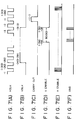
- Fig. 12 of the accompanying drawings shows some examples where a sub picture is displayed in a predetermined area of a main picture.
- a main picture is displayed in a left portion of a screen, and one sub picture is displayed at its lower right end.
- Fig. 12 (B) there are displayed three sub pictures of individually different channels.
- the images of three channels are visually represented as indexes.
- the display method employed in the above two examples is generally termed PoutP (picture-out-picture) since any sub picture is positioned at the end portion of the main picture.
- Fig. 12 (C) and (D) show another display method termed PinP (picture-in-picture).
- a main picture is displayed in a zoom mode with its upper and lower end portions cut, and a sub picture is displayed with partial insertion in the lower right area of the main picture.
- sub pictures are displayed at the four corner areas of the main picture respectively.
- Fig. 13 is a circuit block diagram of a conventional display apparatus for superimposing a sub picture on a parent-picture as mentioned.
- a mixer 101 mixes a sub picture signal with a main picture signal and supplies the mixed signal to an aspect ratio converter 102.
- the aspect ratio converter 102 converts the aspect ratio of the input signal and supplies its output to a double speed converter 103, which converts the input video signal into a double speed signal and outputs the same to a mixer 105 via a switch 104.
- the mixer 105 delivers the input video signal from the double speed converter 103 directly as an output, or mixes a sub picture signal with the input main picture signal of HD-MAC format received via the switch 104 and then outputs the mixed signal therefrom.
- the mixer 101 is supplied with the parent-picture and child-picture video signals of the PAL or NTSC system.
- the substantial picture signal included in such composite video signal is so set as to have, e.g., 720 pixels per horizontal scanning period H.
- the mixer 101 curtails the pixels of the sub picture to, e.g., 240.
- the data of the 240-pixel sub picture (Fig. 14(b)) is inserted in a predetermined region of the 720-pixel main picture (Fig. 14(a)) to thereby produce a new video signal (Fig. 14(c)).
- the data thus obtained is converted by the aspect ratio converter 102 into a signal of a desired aspect ratio. More specifically, in case the aspect ratio of a display unit (not shown) connected to the rear stage of the mixer 105 is 16:9, the video signal of an aspect ratio 4:3 supplied from the mixer 101 is converted into a video signal of an aspect ratio 16:9 (Fig. 14(d)). The converted video signal is inputted to the double speed converter 103, which then produces a video signal of a double field frequency converted as shown in Fig. 14(e). The video signal thus produced is supplied via the switch 104 to the mixer 105, from which the signal is directly outputted to and represented visually on the display unit.
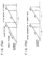
- Fig. 15 shows the principle of such double speed conversion.
- the PAL or NTSC video signal is in a 2:1 interlaced format of 625 lines at 50 Hz, and its aspect ratio is set to 4:3.
- the one-frame video signal of 625 H consists of two video signals of an odd field and an even field each composed of 312.5 H.
- the double speed converter 103 produces, out of the odd-field video signal, two double-frequency odd-field video signals of 313H and 312.5H.
- the converter 103 further produces two even-field video signals of 312H and 312.5H by doubling the frequency of the even-field signal of 312.5H.
- the odd-field video signal of 312.5H is displayed in succession to the odd-field video signal of 313H.
- the even-field video signal of 312H is displayed, which is followed by the even-field video signal of 312.5H. Since the field frequency is doubted as mentioned, it becomes possible to prevent occurrence of flicker.
- the HD-MAC video signal based on the European HD TV standard is in a 2:1 interlaced format of 1250 lines at 50 Hz, and its aspect ratio is set to 16:9.
- the HD-MAC video signal is used for a main picture, it is impossible to employ the mixer 101 in common to the PAL or NTSC system and the HD-MAC system since the number of lines in the former and that in the latter are fundamentally different from each other. Therefore, in using the HD-MAC video signal for a main picture, the circuit configuration is so contrived that the parent-picture video signal is supplied to the mixer 105 via the switch 104, and a child-picture child-picture signal is mixed with the parent-picture signal in the mixer 105.
- a child-picture video signal of 240 pixels is added to a parent-picture video signal of 720 pixels, as shown in Fig. 17(a).
- the length of the mixed signal is rendered greater than the length of 1H.
- memories with a capacity for the data of two fields are required, which raises a problem with regard to an increase of the production cost.
- the video signal shown in Fig. 17(a) may be so processed that its aspect ratio is converted as shown in Fig. 17(b) to remove the overlap on the time base, and then double speed conversion is executed. This process enables a single field memory to be sufficient for the double speed conversion.
- the numbers of lines in such two cases are widely different from each other, fails to achieve common use of the circuit which mixes a sub picture with a main picture, whereby circuits of two systems are needed to increase the production cost.
- the present invention has been accomplished in view of the circumstances mentioned above, and resides in providing an improved display apparatus which is capable of reducing the storage capacity of a memory required for field frequency conversion and of reducing the number of mixer circuits with another advantage of ensuring stable discrimination between even and odd fields.
- a display apparatus comprising a field frequency converter means, preferably a flicker-free processor, for converting the field frequency of a parent-picture video signal; an aspect ratio converter means for converting the aspect ratio of the video signal of which field frequency has been converted by the converter means; child-picture processor means for generating a child-picture video signal; and synthesizer means, preferably a suitably controlled switch, for synthesizing the video signal of which aspect ratio has been converted by the aspect converter, and the video signal obtained from the child-picture processor.
- the field frequency of the parent-picture video signal is converted by the frequency converter, and then the child-picture video signal is synthesized therewith. Consequently the storage capacity of the memory required in the processor can be minimized.
- a display apparatus comprising a field frequency converter means, preferably a flicker-free processor, for converting the field frequency of a parent-picture video signal having a first aspect ratio of, e.g., 4:3; an aspect ratio converter means for converting the aspect ratio 4:3 of the video signal, of which the field frequency has already been converted by the converter means, to a second aspect ratio of, e.g., 16:9; a selector means, preferably a switch, for selecting either the parent-picture video signal of the aspect ratio 16:9 or the parent-picture video signal of which the aspect ratio has been converted by the aspect converter from 4:3 to 16:9; and a synthesizer means, preferably a suitably controlled switch, for synthesizing the video signal obtained from the processor with the video signal of the aspect ratio 16:9 selected by the first-mentioned switch.
- a field frequency converter means preferably a flicker-free processor
- the aspect ratio of the parent-picture video signal is converted by the aspect converter, and then the child-picture video signal obtained from the processor is synthesized with the parent-picture video signal. Therefore, any desired video signal of the aspect ratio 16:9 can be selected by the first-mentioned switch and supplied to the synthesizer switch. As a result, merely one switch is sufficient for synthesizing the sub picture with the main picture.
- a display apparatus comprising a field frequency converter means, preferably a flicker-free processor, for converting the field frequency of a parent-picture video signal; storage means for storing a child-picture video signal; synthesizer means, preferably a switch, for synthesizing the child-picture video signal read out from the storage means with the parent-picture video signal of which the field frequency has already been converted; a field detector means for detecting the odd fields and the even fields with respect to the parent-picture video signal prior to the field frequency conversion; and a processor for controlling the reading from memories of the storage means in accordance with the output of the detection circuit.
- a field frequency converter means preferably a flicker-free processor
- discrimination between the odd fields and the even fields can be executed on the basis of the parent-picture video signal prior to the field frequency conversion. And the operation of reading out the signal from the memories is controlled in accordance with the result of such discrimination. Consequently the discrimination between the odd and even fields can be performed with accuracy, and the circuit configuration for such control can be simplified.
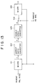
- Fig. 1 is a block diagram showing the constitution of an exemplary embodiment which represents the display apparatus of the present invention.
- An antenna 1 serves to receive UHF and VHF television broadcast waves, while an antenna 2 serves to receive satellite broadcast waves.
- a tuner 3 receives the outputs of the antennas 1, 2 and supplies its detected output to one input terminal of a switch 4, to which are also supplied, in addition to the output of the tuner 3, video signals 1 through 3 from an unshown VTR or the like.
- the switch 4 selects one of the inputs supplied thereto and delivers the selected signal to decoders 6 and 7.
- the decoder 6 decodes the parent-picture video signal supplied from the switch 4 and outputs the decoded signal to a flicker-free processor 8.
- the decoder 6 is so formed as to be capable of decoding any of PAL, NTSC and D2-MAC video signals.
- the flicker-free processor 8 serves to double the field frequency of the video signal supplied from the decoder 6 and outputs the frequency-converted signal.
- an aspect converter 9 converts the aspect ratio of the input frequency-doubled video signal to 16:9 in case the ratio thereof is 4:3. When the aspect ratio of the input video signal is 16:9, the signal is outputted directly without any conversion of the aspect ratio.
- a switch 5 selects one of HD TV signals of the HD-MAC format and so forth supplied from an unshown apparatus, and outputs the selected signal to switches 10 and 11.
- the switch 10 selects either the video signal supplied from the switch 5 or the video signal from the aspect converter 9, and supplies the selected signal to one input terminal of a switch 13. More specifically, the aspect ratio of the video signal supplied to each input terminal of the switch 10 is so processed as to be 16:9. Therefore the video signal supplied to one input terminal of the switch 13 always has an aspect ratio of 16:9.
- the decoder 7 decodes the video signal selected by the switch 4 and supplies the selected signal to the other input terminal of the switch 11.
- the HD TV video signal selected by the switch 5 is supplied to one terminal of the switch 11. Therefore the switch 11 selects one of the input signals and outputs the same to the PinP processor 12, which then generates a child-picture video signal from the input video signal.
- the processor 12 detects a vertical synchronizing signal and a vertical synchronizing signal from the parent-picture video signal supplied thereto via the switch 10.
- the child-picture video signal obtained from the processor 12 is supplied to the other input terminal of the switch 13.
- the switch 13 is changed at a predetermined timing to the upper or lower position in Fig. 1 and synthesizes the child-picture video signal, which is supplied from the processor 12, with the parent-picture video signal obtained from the switch 10, and then delivers the synthesized signal to a video processor 14. Subsequently the video signal processed by the video processor 14 is outputted to and displayed on a CRT 15 which has an aspect ratio of 16:9.
- a deflector 16 detects the vertical and horizontal synchronizing signals from the output of the switch 13 and controls the scanning on the CRT 15 in accordance with the detected signals.
- a switch 17 selects the vertical and horizontal synchronizing signals included in the video signal outputted from the flicker-free processor 8 or the deflector 16 prior to the field signal conversion and delivers the selected signals to the processor 12.
- the main picture video signal is supplied to the switch 10 via the decoder 6, the processor 8 and the aspect converter 9, or directly from the switch 5 without being passed through any of such circuits.
- the child-picture video signal is processed by the processor 12 independently of the main picture. Therefore, no fundamental difference is existent between the operation in the PinP mode and that in the PoutP mode, and the difference is concerned merely with the switching timing of the switch 13.
- Fig. 2 is a timing chart for explaining the one-line operation in synthesizing the child-picture video signal with the parent-picture video signal.
- the parent-picture video signal shown in Fig. 2(a) is such that the number of pixels during the time of the effective video signal out of the 1H period is set to 720.
- Such video signal is supplied from the decoder 6 to the processor 8, which then converts the input signal into a video signal of Fig. 2(b) having a double field frequency. This frequency conversion is performed by reading out the data of 720 pixels in conformity with clock pulses of a double frequency.
- the video signal of which field frequency has been doubted by the flicker-free processor 8, is then supplied to the aspect converter 9 where a video signal of Fig. 2(c) is produced with its aspect ratio so converted as shown.
- the processor 12 there is generated a child-picture video signal composed of 240 pixels as shown in Fig. 2(d).
- the switch 13 is changed to the upper position in Fig. 1 when selecting the parent-picture video signal, or is changed to the lower position in the same diagram when selecting the child-picture video signal. Consequently, the video signal outputted from the switch 13 is such as shown in Fig. 2(e) where the effective video signal per line of the synthesized parent and sub pictures is composed of 720 pixels.
- Fig. 3 shows a further detailed constitution of the processor 12 employed in the apparatus of Fig. 1.
- the luminance (Y) signal in the child-picture video signal outputted from the switch 11 is supplied to an A-D converter 21 and, after analog-to-digital conversion, the resultant digital signal is written pixel by pixel in memories 23 and 24 alternately.
- the colour difference signals PB and PR are supplied to an A-D converter 22 and, after analog-to-digital conversion, the digital signals are written in a memory 25.
- the child-picture horizontal synchronizing signal is supplied to a write-side PLL 26, which then generates write clock pulses of a frequency 14.3 MHz in synchronism with the horizontal synchronizing signal.
- a processor 40 controls the operation of writing in the memories 23 to 25 in synchronism with the write clock pulses obtained from the PLL 26.
- a read-side PLL 27 generates pulses of a frequency 28.6 MHz (double the frequency of the write clock pulses generated by the write-side PLL 26) synchronized with the horizontal synchronizing signal included in the parent-picture video signal inputted from the switch 17, and then supplies such double-frequency pulses to the processor 40, to which the vertical synchronizing signal of the parent-picture video signal is also supplied from the switch 17.
- the processor 40 reads out the data from the memories 23 to 25 in synchronism with the input signals. Out of the data thus read, the luminance signal component is supplied to a D-A converter 28 and, after digital-to-analog conversion, the luminance signal is outputted therefrom.
- the colour difference signal PB is supplied to a D-A converter 29 for digital-to-analog conversion, while the other colour difference signal PR is supplied to a D-A converter 30 for digital-to-analog conversion.
- the signals thus converted are outputted from the converters 29 and 30 respectively.
- the first-frame data is composed of the first-field data of 128 dots x 160 lines written in the area 1 and the second-field data of 128 dots x 160 lines written in the area 2.
- the second-frame data is composed of the first-field data of 128 dots x 160 lines written in the area 3 and the second-field data of 128 dots x 160 lines in the area 4.
- Such writing operation is performed sequentially and continuously in the order of the areas 1 - 2 - 3 - 4 - 1 - 2 - 3 - 4 and so forth as shown in Fig. 4(A).
- the reading operation is performed initially in the order of the areas 1 - 2 - 3 - 4 as shown in Fig. 4(B) and, after repeated reading from the areas 3 and 4, the operation is continued in the order of the areas 1 - 2 - 3 - 4 again. Due to such repeated operation of reading the data from the areas 3 and 4 twice, it becomes possible to avert a trouble that the read address passes the write address.
- the operation of reading out the data of four fields is controlled in conformity with the result of discrimination between the odd and even fields performed by the detector 70 shown in Fig. 9 which will be described rater. More specifically, the data are read out from the areas 1 and 3 in response to detection of the odd fields by the detector 70, or from the areas 2 and 4 in response to detection of the even fields.
- Fig. 5 shows an exemplary read-side constitution of the processor 12 employed in the apparatus of Fig. 1.
- a read-side PLL 27 generates clock pulses synchronized with the horizontal synchronizing signal included in the parent-picture video signal supplied from the switch 17. More specifically, a clock generator 54 generates clock pulses of Fig. 6(A) and supplies the same to an H counter 55, where a value -910 is initially loaded at a predetermined timing. Thereafter the clock pulses supplied from the clock generator 54 are counted, and the count is incremented by 1 per pulse.
- a logical low-level signal is outputted when the count is in a range of -910 to -455, or a logical high-level signal is outputted when the count is in a range of -454 to -1, as shown in Fig. 6(B).
- the signal thus obtained is compared by a phase comparator 51 with the horizontal synchronizing signal included in the parent-picture video signal supplied from the switch 17.
- the resultant phase difference is first smoothened through a low-pass filter 52 and is supplied to a VCO (voltage-controlled oscillator) 53, which then generates clock pulses of a frequency (28.6 MHz) corresponding to the phase difference.
- the clock pulses thus obtained are supplied to the clock generator 54, which then generates the aforementioned clock pulses of Fig. 6(A) in synchronism with the input clock pulses.
- the H counter 55 generates an HCLK signal of Fig. 6(C) whose phase is inverse to that of the signal shown in Fig. 6(B), and supplies such HCLK signal to both a V counter 56 and a V enable circuit 57.
- the H counter 55 further generates an H enable signal of Fig. 6(D) which is turned to a logical high level in response to a counted value of -430 to -190 or is turned to a logical low level in response to any other counted value.
- Such H enable signal is supplied to one input terminal of an AND gate 58.
- the V counter 56 counts the HCLK signal of Fig. 7(A) supplied from the H counter 55.
- the V counter 56 there is loaded a value -263 when the child-picture video signal is of the NTSC system, or a value -313 when such video signal is of the PAL system. And its count is incremented by 1 every time the HCLK signal is counted.
- the V counter 56 generates a VBLK signal of Fig. 7(B) which is turned to a logical high level when the counted value in the NTSC system ranges from -243 to -3 (or from -291 to -3 in the PAL system), or is turned to a logical low level when the count is any other value.
- This VBLK signal corresponds to the vertical blanking interval.
- the V counter 56 When the counted value has reached -1, the V counter 56 generates a CARRY signal shown in Fig. 7(C).
- the V enable circuit 57 counts the HCLK signal (Fig. 7(A)) and generates a V enable signal (Fig. 7(D)) which is turned to a logical high level when the counted value in the NTSC system ranges from -118 to -38 (or from -134 to -38 in the PAL system), or is turned to a logical low level when the count is any other value.
- V enable signal is supplied to one input terminal of an AND gate 58.
- the H enable signal (Fig. 7(E)) obtained from the H counter 55, and the AND gate 58 permits the H enable signal to pass therethrough during the supply of the high-level V enable signal from the V enable circuit 57.
- a timing signal generator 59 generates clock pulses SOCYl (Fig. 8(B)) for reading out the data from the memory 23 shown in Fig. 1 during the logical high level of the H enable signal (Fig. 8(A)) supplied via the AND gate 58, and also generates clock pulses SOCY2 (Fig. 8(C)) for reading out the data from the memory 24 during the same time.
- Such two clock signals SOCYl and SOCY2 are so formed that the respective phases are inverse to each other.
- the timing signal generator 59 further generates a signal SOE (Fig. 8(D)) which is inverse in phase to the H enable signal (Fig. 8(A)) supplied from the AND gate 58.
- the SOE signal is supplied from the AND gate 58.
- the SOE signal is supplied to the memories 23 and 24 as an enable signal to permit the data reading when its logical level is low.
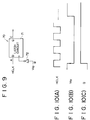
- Fig. 9 shows an exemplary constitution of the detector 70 included in the processor 12.
- the detector 70 comprises a latch circuit 71 and an inverter 72.
- the HCLK signal (Fig. 10(A)) generated from the H counter 55 is inputted to a terminal D of the latch circuit 71.
- the vertical synchronizing signal (Fig. 10(B)) of the parent-picture video signal (prior to the field frequency conversion) outputted from the switch 17 is supplied to the inverter 72.
- the logical level of the HCLK signal is high at the trailing-edge timing of the vertical synchronizing signal. Therefore the Q output of the latch circuit 71 is turned to a logical high level as shown in Fig. 10(C).
- the HCLK signal (Fig. 11(A)) at the trailing edge of the vertical synchronizing signal (Fig. 11(B)) has a logical low level as shown, so that the Q output of the latch circuit 71 is turned to a logical low level. Consequently, a detection signal signifying an odd field or an even field of the parent-picture video signal is delivered from the Q output of the input circuit 71.
- the parent-picture video signal is synchronized with the child-picture video signal after conversion of the field frequency, so that the storage capacity of the memory means can be minimized in the process of the field frequency conversion.
- discrimination between odd and even fields is executed with respect to the parent-picture video signal prior to the field frequency conversion thereof, whereby a high accuracy is attained in the discrimination with another advantage of simplifying the circuit configuration to eventually reduce the production cost of the apparatus.
Abstract
Description
- The present invention relates to a display apparatus having a picture-in-picture or picture-out-picture function for superimposing a sub picture on a main picture being displayed on a screen of a television receiver or the like.
- Fig. 12 of the accompanying drawings shows some examples where a sub picture is displayed in a predetermined area of a main picture. In Fig. 12 (A), a main picture is displayed in a left portion of a screen, and one sub picture is displayed at its lower right end. Next in Fig. 12 (B), there are displayed three sub pictures of individually different channels. In this example, the images of three channels are visually represented as indexes. The display method employed in the above two examples is generally termed PoutP (picture-out-picture) since any sub picture is positioned at the end portion of the main picture.
- Fig. 12 (C) and (D) show another display method termed PinP (picture-in-picture). In the example (C), a main picture is displayed in a zoom mode with its upper and lower end portions cut, and a sub picture is displayed with partial insertion in the lower right area of the main picture. Further in the example (D), sub pictures are displayed at the four corner areas of the main picture respectively.
- Fig. 13 is a circuit block diagram of a conventional display apparatus for superimposing a sub picture on a parent-picture as mentioned. In this example, a
mixer 101 mixes a sub picture signal with a main picture signal and supplies the mixed signal to anaspect ratio converter 102. Then theaspect ratio converter 102 converts the aspect ratio of the input signal and supplies its output to adouble speed converter 103, which converts the input video signal into a double speed signal and outputs the same to amixer 105 via aswitch 104. Subsequently themixer 105 delivers the input video signal from thedouble speed converter 103 directly as an output, or mixes a sub picture signal with the input main picture signal of HD-MAC format received via theswitch 104 and then outputs the mixed signal therefrom. - Now the operation of the above conventional apparatus will be described below with reference to a timing chart of Fig. 14. The
mixer 101 is supplied with the parent-picture and child-picture video signals of the PAL or NTSC system. The substantial picture signal included in such composite video signal is so set as to have, e.g., 720 pixels per horizontal scanning period H. Themixer 101 curtails the pixels of the sub picture to, e.g., 240. The data of the 240-pixel sub picture (Fig. 14(b)) is inserted in a predetermined region of the 720-pixel main picture (Fig. 14(a)) to thereby produce a new video signal (Fig. 14(c)). - The data thus obtained is converted by the
aspect ratio converter 102 into a signal of a desired aspect ratio. More specifically, in case the aspect ratio of a display unit (not shown) connected to the rear stage of themixer 105 is 16:9, the video signal of an aspect ratio 4:3 supplied from themixer 101 is converted into a video signal of an aspect ratio 16:9 (Fig. 14(d)). The converted video signal is inputted to thedouble speed converter 103, which then produces a video signal of a double field frequency converted as shown in Fig. 14(e). The video signal thus produced is supplied via theswitch 104 to themixer 105, from which the signal is directly outputted to and represented visually on the display unit. - Fig. 15 shows the principle of such double speed conversion. The PAL or NTSC video signal is in a 2:1 interlaced format of 625 lines at 50 Hz, and its aspect ratio is set to 4:3. The one-frame video signal of 625 H consists of two video signals of an odd field and an even field each composed of 312.5 H. The
double speed converter 103 produces, out of the odd-field video signal, two double-frequency odd-field video signals of 313H and 312.5H. Theconverter 103 further produces two even-field video signals of 312H and 312.5H by doubling the frequency of the even-field signal of 312.5H. - Consequently, as shown in Fig. 16, the odd-field video signal of 312.5H is displayed in succession to the odd-field video signal of 313H. Subsequently the even-field video signal of 312H is displayed, which is followed by the even-field video signal of 312.5H. Since the field frequency is doubted as mentioned, it becomes possible to prevent occurrence of flicker.
- Meanwhile the HD-MAC video signal based on the European HD TV standard is in a 2:1 interlaced format of 1250 lines at 50 Hz, and its aspect ratio is set to 16:9. In case the HD-MAC video signal is used for a main picture, it is impossible to employ the
mixer 101 in common to the PAL or NTSC system and the HD-MAC system since the number of lines in the former and that in the latter are fundamentally different from each other. Therefore, in using the HD-MAC video signal for a main picture, the circuit configuration is so contrived that the parent-picture video signal is supplied to themixer 105 via theswitch 104, and a child-picture child-picture signal is mixed with the parent-picture signal in themixer 105. - In displaying a sub picture to a main picture in the PoutP mode, a child-picture video signal of 240 pixels is added to a parent-picture video signal of 720 pixels, as shown in Fig. 17(a). It follows therefrom that the length of the mixed signal is rendered greater than the length of 1H. Accordingly, for double speed conversion of such signal, there exists the necessity of providing two field memories in the double speed converter and writing the data therein alternately per line. For this purpose, memories with a capacity for the data of two fields are required, which raises a problem with regard to an increase of the production cost. In an attempt to eliminate such disadvantage, the video signal shown in Fig. 17(a) may be so processed that its aspect ratio is converted as shown in Fig. 17(b) to remove the overlap on the time base, and then double speed conversion is executed. This process enables a single field memory to be sufficient for the double speed conversion.
- However, since the number of pixels of the lH data inputted to the
double speed converter 103 is 960 (= 720 + 240), the storage capacity of the memory employed in thedouble speed converter 103 needs to be 4/3 (= 960/720) times the 720 pixels required for the display in the picture-in-picture mode. Consequently the problem of the high production cost is still left unsolved. - Furthermore, in one case of using the HD-MAC video signal for a main picture and another case of using the NTSC or PAL video signal for a main picture, the numbers of lines in such two cases are widely different from each other, fails to achieve common use of the circuit which mixes a sub picture with a main picture, whereby circuits of two systems are needed to increase the production cost.
- In addition, if the frequency-converted video signals are employed for discrimination between the odd and even fields of the video signals posterior to conversion of the field frequency, it becomes necessary to discriminate among 312.5H, 313H, 312.5H and 312H to consequently require a greater circuit scale, hence causing difficulties in realization of stable discrimination.
- The present invention has been accomplished in view of the circumstances mentioned above, and resides in providing an improved display apparatus which is capable of reducing the storage capacity of a memory required for field frequency conversion and of reducing the number of mixer circuits with another advantage of ensuring stable discrimination between even and odd fields.
- According to a first aspect of the present invention, there is provided a display apparatus comprising a field frequency converter means, preferably a flicker-free processor, for converting the field frequency of a parent-picture video signal; an aspect ratio converter means for converting the aspect ratio of the video signal of which field frequency has been converted by the converter means; child-picture processor means for generating a child-picture video signal; and synthesizer means, preferably a suitably controlled switch, for synthesizing the video signal of which aspect ratio has been converted by the aspect converter, and the video signal obtained from the child-picture processor. In this display apparatus, the field frequency of the parent-picture video signal is converted by the frequency converter, and then the child-picture video signal is synthesized therewith. Consequently the storage capacity of the memory required in the processor can be minimized.
- According to a second aspect of the present invention, there is provided a display apparatus comprising a field frequency converter means, preferably a flicker-free processor, for converting the field frequency of a parent-picture video signal having a first aspect ratio of, e.g., 4:3; an aspect ratio converter means for converting the aspect ratio 4:3 of the video signal, of which the field frequency has already been converted by the converter means, to a second aspect ratio of, e.g., 16:9; a selector means, preferably a switch, for selecting either the parent-picture video signal of the aspect ratio 16:9 or the parent-picture video signal of which the aspect ratio has been converted by the aspect converter from 4:3 to 16:9; and a synthesizer means, preferably a suitably controlled switch, for synthesizing the video signal obtained from the processor with the video signal of the aspect ratio 16:9 selected by the first-mentioned switch. In this display apparatus, first the aspect ratio of the parent-picture video signal is converted by the aspect converter, and then the child-picture video signal obtained from the processor is synthesized with the parent-picture video signal. Therefore, any desired video signal of the aspect ratio 16:9 can be selected by the first-mentioned switch and supplied to the synthesizer switch. As a result, merely one switch is sufficient for synthesizing the sub picture with the main picture.
- According to a third aspect of the present invention, there is provided a display apparatus comprising a field frequency converter means, preferably a flicker-free processor, for converting the field frequency of a parent-picture video signal; storage means for storing a child-picture video signal; synthesizer means, preferably a switch, for synthesizing the child-picture video signal read out from the storage means with the parent-picture video signal of which the field frequency has already been converted; a field detector means for detecting the odd fields and the even fields with respect to the parent-picture video signal prior to the field frequency conversion; and a processor for controlling the reading from memories of the storage means in accordance with the output of the detection circuit. In this display apparatus, discrimination between the odd fields and the even fields can be executed on the basis of the parent-picture video signal prior to the field frequency conversion. And the operation of reading out the signal from the memories is controlled in accordance with the result of such discrimination. Consequently the discrimination between the odd and even fields can be performed with accuracy, and the circuit configuration for such control can be simplified.
- The invention will be further described by way of non-limitative example with reference to the accompanying drawings, in which:-
- Fig. 1 is a block diagram of an embodiment of display apparatus according to the present invention;
- Fig. 2 is a timing chart of signals for explaining the operation of the embodiment shown in Fig. 1;
- Fig. 3 is a block diagram of a PinP processor employed in the embodiment of Fig. 1;
- Fig. 4 is a timing chart of signals for explaining the operation of the PinP processor shown in Fig. 3;
- Fig. 5 is a block diagram of a reading circuit configuration of the PinP processor employed in the embodiment of Fig. 1;
- Fig. 6 is a timing chart of signals for explaining the operation of the PinP processor shown in Fig. 5;
- Fig. 7 is another timing chart of signals for explaining the operation of the PinP processor shown in Fig. 5;
- Fig. 8 is a further timing chart of signals for explaining the operation of the PinP processor shown in Fig. 5;
- Fig. 9 is a block diagram showing the constitution of a detector included in the PinP processor of Fig. 1;
- Fig. 10 is a timing chart of signals for explaining the operation of the detector shown in Fig. 9;
- Fig. 11 is another timing chart of signals for explaining the operation of the detector shown in Fig. 9;
- Fig. 12 (A) through (D) illustrate examples of display modes where a sub picture is superimposed on a main picture;
- Fig. 13 is a block diagram of an exemplary conventional display apparatus;
- Fig. 14 is a timing chart of signals for explaining the operation of the display apparatus shown in Fig. 13;
- Fig. 15 is another timing chart of signals for explaining the operation of the display apparatus shown in Fig. 13;
- Fig. 16 illustrates scanning lines in the conversion of a field frequency in the apparatus of Fig. 13; and
- Fig. 17 illustrates signals in a PoutP display mode.
- Fig. 1 is a block diagram showing the constitution of an exemplary embodiment which represents the display apparatus of the present invention. An
antenna 1 serves to receive UHF and VHF television broadcast waves, while anantenna 2 serves to receive satellite broadcast waves. Atuner 3 receives the outputs of theantennas switch 4, to which are also supplied, in addition to the output of thetuner 3,video signals 1 through 3 from an unshown VTR or the like. Theswitch 4 selects one of the inputs supplied thereto and delivers the selected signal todecoders - The
decoder 6 decodes the parent-picture video signal supplied from theswitch 4 and outputs the decoded signal to a flicker-free processor 8. In this embodiment, thedecoder 6 is so formed as to be capable of decoding any of PAL, NTSC and D2-MAC video signals. The flicker-free processor 8 serves to double the field frequency of the video signal supplied from thedecoder 6 and outputs the frequency-converted signal. And anaspect converter 9 converts the aspect ratio of the input frequency-doubled video signal to 16:9 in case the ratio thereof is 4:3. When the aspect ratio of the input video signal is 16:9, the signal is outputted directly without any conversion of the aspect ratio. - A
switch 5 selects one of HD TV signals of the HD-MAC format and so forth supplied from an unshown apparatus, and outputs the selected signal toswitches switch 10 selects either the video signal supplied from theswitch 5 or the video signal from theaspect converter 9, and supplies the selected signal to one input terminal of aswitch 13. More specifically, the aspect ratio of the video signal supplied to each input terminal of theswitch 10 is so processed as to be 16:9. Therefore the video signal supplied to one input terminal of theswitch 13 always has an aspect ratio of 16:9. - Meanwhile the
decoder 7 decodes the video signal selected by theswitch 4 and supplies the selected signal to the other input terminal of theswitch 11. As described above, the HD TV video signal selected by theswitch 5 is supplied to one terminal of theswitch 11. Therefore theswitch 11 selects one of the input signals and outputs the same to thePinP processor 12, which then generates a child-picture video signal from the input video signal. For generating such child-picture video signal, theprocessor 12 detects a vertical synchronizing signal and a vertical synchronizing signal from the parent-picture video signal supplied thereto via theswitch 10. - The child-picture video signal obtained from the
processor 12 is supplied to the other input terminal of theswitch 13. Theswitch 13 is changed at a predetermined timing to the upper or lower position in Fig. 1 and synthesizes the child-picture video signal, which is supplied from theprocessor 12, with the parent-picture video signal obtained from theswitch 10, and then delivers the synthesized signal to avideo processor 14. Subsequently the video signal processed by thevideo processor 14 is outputted to and displayed on aCRT 15 which has an aspect ratio of 16:9. - A
deflector 16 detects the vertical and horizontal synchronizing signals from the output of theswitch 13 and controls the scanning on theCRT 15 in accordance with the detected signals. Aswitch 17 selects the vertical and horizontal synchronizing signals included in the video signal outputted from the flicker-free processor 8 or thedeflector 16 prior to the field signal conversion and delivers the selected signals to theprocessor 12. - In this embodiment, the main picture video signal is supplied to the
switch 10 via thedecoder 6, theprocessor 8 and theaspect converter 9, or directly from theswitch 5 without being passed through any of such circuits. And the child-picture video signal is processed by theprocessor 12 independently of the main picture. Therefore, no fundamental difference is existent between the operation in the PinP mode and that in the PoutP mode, and the difference is concerned merely with the switching timing of theswitch 13. - Fig. 2 is a timing chart for explaining the one-line operation in synthesizing the child-picture video signal with the parent-picture video signal. The parent-picture video signal shown in Fig. 2(a) is such that the number of pixels during the time of the effective video signal out of the 1H period is set to 720. Such video signal is supplied from the
decoder 6 to theprocessor 8, which then converts the input signal into a video signal of Fig. 2(b) having a double field frequency. This frequency conversion is performed by reading out the data of 720 pixels in conformity with clock pulses of a double frequency. As far as this process is concerned, there is no difference between the PinP mode and the PoutP mode as described, so that the required storage capacity of the memory incorporated in theprocessor 8 corresponds merely to the data of one field. - The video signal, of which field frequency has been doubted by the flicker-
free processor 8, is then supplied to theaspect converter 9 where a video signal of Fig. 2(c) is produced with its aspect ratio so converted as shown. Meanwhile in theprocessor 12, there is generated a child-picture video signal composed of 240 pixels as shown in Fig. 2(d). Theswitch 13 is changed to the upper position in Fig. 1 when selecting the parent-picture video signal, or is changed to the lower position in the same diagram when selecting the child-picture video signal. Consequently, the video signal outputted from theswitch 13 is such as shown in Fig. 2(e) where the effective video signal per line of the synthesized parent and sub pictures is composed of 720 pixels. - Fig. 3 shows a further detailed constitution of the
processor 12 employed in the apparatus of Fig. 1. The luminance (Y) signal in the child-picture video signal outputted from theswitch 11 is supplied to anA-D converter 21 and, after analog-to-digital conversion, the resultant digital signal is written pixel by pixel inmemories A-D converter 22 and, after analog-to-digital conversion, the digital signals are written in amemory 25. The child-picture horizontal synchronizing signal is supplied to a write-side PLL 26, which then generates write clock pulses of a frequency 14.3 MHz in synchronism with the horizontal synchronizing signal. Aprocessor 40 controls the operation of writing in thememories 23 to 25 in synchronism with the write clock pulses obtained from thePLL 26. To thememories 23 to 25, there are inputted the data of 320 lines each composed of 256 pixels. And each of such pixels consists of 6 bits. - Meanwhile a read-
side PLL 27 generates pulses of a frequency 28.6 MHz (double the frequency of the write clock pulses generated by the write-side PLL 26) synchronized with the horizontal synchronizing signal included in the parent-picture video signal inputted from theswitch 17, and then supplies such double-frequency pulses to theprocessor 40, to which the vertical synchronizing signal of the parent-picture video signal is also supplied from theswitch 17. Theprocessor 40 reads out the data from thememories 23 to 25 in synchronism with the input signals. Out of the data thus read, the luminance signal component is supplied to aD-A converter 28 and, after digital-to-analog conversion, the luminance signal is outputted therefrom. The colour difference signal PB is supplied to aD-A converter 29 for digital-to-analog conversion, while the other colour difference signal PR is supplied to aD-A converter 30 for digital-to-analog conversion. The signals thus converted are outputted from theconverters - When the first pixel data of the luminance signal is written in the
memory 23 for example, the next second pixel data thereof is written in thememory 24. Thereafter the luminance signal is written pixel by pixel alternately in such a manner that the third pixel data is written in thememory 23, and then the fourth pixel data in thememory 24. Consequently, as shown in Fig. 4(C), the first-frame data is composed of the first-field data of 128 dots x 160 lines written in thearea 1 and the second-field data of 128 dots x 160 lines written in thearea 2. Similarly, the second-frame data is composed of the first-field data of 128 dots x 160 lines written in thearea 3 and the second-field data of 128 dots x 160 lines in thearea 4. Such writing operation is performed sequentially and continuously in the order of the areas 1 - 2 - 3 - 4 - 1 - 2 - 3 - 4 and so forth as shown in Fig. 4(A). - In contrast with the above, the reading operation is performed initially in the order of the areas 1 - 2 - 3 - 4 as shown in Fig. 4(B) and, after repeated reading from the
areas areas - The operation of reading out the data of four fields is controlled in conformity with the result of discrimination between the odd and even fields performed by the
detector 70 shown in Fig. 9 which will be described rater. More specifically, the data are read out from theareas detector 70, or from theareas - Fig. 5 shows an exemplary read-side constitution of the
processor 12 employed in the apparatus of Fig. 1. A read-side PLL 27 generates clock pulses synchronized with the horizontal synchronizing signal included in the parent-picture video signal supplied from theswitch 17. More specifically, aclock generator 54 generates clock pulses of Fig. 6(A) and supplies the same to anH counter 55, where a value -910 is initially loaded at a predetermined timing. Thereafter the clock pulses supplied from theclock generator 54 are counted, and the count is incremented by 1 per pulse. And a logical low-level signal is outputted when the count is in a range of -910 to -455, or a logical high-level signal is outputted when the count is in a range of -454 to -1, as shown in Fig. 6(B). The signal thus obtained is compared by aphase comparator 51 with the horizontal synchronizing signal included in the parent-picture video signal supplied from theswitch 17. The resultant phase difference is first smoothened through a low-pass filter 52 and is supplied to a VCO (voltage-controlled oscillator) 53, which then generates clock pulses of a frequency (28.6 MHz) corresponding to the phase difference. The clock pulses thus obtained are supplied to theclock generator 54, which then generates the aforementioned clock pulses of Fig. 6(A) in synchronism with the input clock pulses. - The
H counter 55 generates an HCLK signal of Fig. 6(C) whose phase is inverse to that of the signal shown in Fig. 6(B), and supplies such HCLK signal to both aV counter 56 and a V enablecircuit 57. The H counter 55 further generates an H enable signal of Fig. 6(D) which is turned to a logical high level in response to a counted value of -430 to -190 or is turned to a logical low level in response to any other counted value. Such H enable signal is supplied to one input terminal of an ANDgate 58. - The V counter 56 counts the HCLK signal of Fig. 7(A) supplied from the
H counter 55. In theV counter 56, there is loaded a value -263 when the child-picture video signal is of the NTSC system, or a value -313 when such video signal is of the PAL system. And its count is incremented by 1 every time the HCLK signal is counted. TheV counter 56 generates a VBLK signal of Fig. 7(B) which is turned to a logical high level when the counted value in the NTSC system ranges from -243 to -3 (or from -291 to -3 in the PAL system), or is turned to a logical low level when the count is any other value. This VBLK signal corresponds to the vertical blanking interval. When the counted value has reached -1, theV counter 56 generates a CARRY signal shown in Fig. 7(C). - Meanwhile the V enable
circuit 57 counts the HCLK signal (Fig. 7(A)) and generates a V enable signal (Fig. 7(D)) which is turned to a logical high level when the counted value in the NTSC system ranges from -118 to -38 (or from -134 to -38 in the PAL system), or is turned to a logical low level when the count is any other value. Such V enable signal is supplied to one input terminal of an ANDgate 58. Meanwhile to the other input terminal of the ANDgate 58 is supplied the H enable signal (Fig. 7(E)) obtained from theH counter 55, and the ANDgate 58 permits the H enable signal to pass therethrough during the supply of the high-level V enable signal from the V enablecircuit 57. - A
timing signal generator 59 generates clock pulses SOCYl (Fig. 8(B)) for reading out the data from thememory 23 shown in Fig. 1 during the logical high level of the H enable signal (Fig. 8(A)) supplied via the ANDgate 58, and also generates clock pulses SOCY2 (Fig. 8(C)) for reading out the data from thememory 24 during the same time. Such two clock signals SOCYl and SOCY2 are so formed that the respective phases are inverse to each other. Thetiming signal generator 59 further generates a signal SOE (Fig. 8(D)) which is inverse in phase to the H enable signal (Fig. 8(A)) supplied from the ANDgate 58. The SOE signal is supplied from the ANDgate 58. The SOE signal is supplied to thememories - Fig. 9 shows an exemplary constitution of the
detector 70 included in theprocessor 12. Thedetector 70 comprises alatch circuit 71 and aninverter 72. The HCLK signal (Fig. 10(A)) generated from theH counter 55 is inputted to a terminal D of thelatch circuit 71. And the vertical synchronizing signal (Fig. 10(B)) of the parent-picture video signal (prior to the field frequency conversion) outputted from theswitch 17 is supplied to theinverter 72. In case the field of the main picture is an odd one, the logical level of the HCLK signal is high at the trailing-edge timing of the vertical synchronizing signal. Therefore the Q output of thelatch circuit 71 is turned to a logical high level as shown in Fig. 10(C). - When the field of the parent-picture video signal is an even one, the HCLK signal (Fig. 11(A)) at the trailing edge of the vertical synchronizing signal (Fig. 11(B)) has a logical low level as shown, so that the Q output of the
latch circuit 71 is turned to a logical low level. Consequently, a detection signal signifying an odd field or an even field of the parent-picture video signal is delivered from the Q output of theinput circuit 71. - According to the present invention, as described hereinabove, the parent-picture video signal is synchronized with the child-picture video signal after conversion of the field frequency, so that the storage capacity of the memory means can be minimized in the process of the field frequency conversion.
- Furthermore, due to the procedure of synthesizing the parent-picture video signal with the child-picture video signal after conversion of the aspect ratio, a single synthesizing means is sufficient to meet the requirement regardless of any aspect ratio of the main picture.
- In addition, discrimination between odd and even fields is executed with respect to the parent-picture video signal prior to the field frequency conversion thereof, whereby a high accuracy is attained in the discrimination with another advantage of simplifying the circuit configuration to eventually reduce the production cost of the apparatus.
Claims (3)
- A display apparatus comprising:
a field frequency converter means for converting the field frequency of a parent-picture video signal;
an aspect ratio converter means for converting the aspect ratio of the video signal posterior to the field frequency conversion by said field frequency converter means;
a child-picture processor means for generating a child-picture video signal; and
a synthesizer means for synthesizing the video signal of which the aspect ratio has been converted by said aspect converter means, with the video signal obtained from said child-picture processor means. - A display apparatus comprising:
a field frequency converter means for converting the field frequency of a parent-picture video signal having a first aspect ratio;
an aspect ratio converter means for converting the aspect ratio of the video signal, of which the field frequency has been converted by said field frequency converter means, to a second aspect ratio;
a selector means for selecting either the parent-picture video signal of said second aspect ratio or the parent-picture video signal of which the first aspect ratio has been converted by said aspect ratio converter means to said second aspect ratio;
a child-picture processor means for generating a child-picture video signal; and
a synthesizer means for synthesizing the video signal obtained from said child-picture processor means with the video signal of said second aspect ratio selected by said selector means. - A display apparatus comprising:
a frequency converter means for converting the field frequency of a parent-picture video signal;
a memory means for storing a child-picture video signal;
a synthesizer means for synthesizing the child-picture video signal read out from said memory means with the parent-picture video signal posterior to the field frequency conversion thereof;
a field detector means for detecting the odd fields and the even fields with respect to the parent-picture video signal prior to the field frequency conversion thereof; and
a control means for controlling the reading from said memory means in accordance with the output of said field detector means.
Applications Claiming Priority (2)
| Application Number | Priority Date | Filing Date | Title |
|---|---|---|---|
| JP4018539A JPH05183833A (en) | 1992-01-07 | 1992-01-07 | Display device |
| JP18539/92 | 1992-01-07 |
Publications (2)
| Publication Number | Publication Date |
|---|---|
| EP0551168A1 true EP0551168A1 (en) | 1993-07-14 |
| EP0551168B1 EP0551168B1 (en) | 1998-07-08 |
Family
ID=11974434
Family Applications (1)
| Application Number | Title | Priority Date | Filing Date |
|---|---|---|---|
| EP93300002A Revoked EP0551168B1 (en) | 1992-01-07 | 1993-01-04 | Display apparatus |
Country Status (4)
| Country | Link |
|---|---|
| US (2) | US5420641A (en) |
| EP (1) | EP0551168B1 (en) |
| JP (1) | JPH05183833A (en) |
| DE (1) | DE69319452T2 (en) |
Cited By (7)
| Publication number | Priority date | Publication date | Assignee | Title |
|---|---|---|---|---|
| EP0660601A2 (en) * | 1993-12-24 | 1995-06-28 | Kabushiki Kaisha Toshiba | Video processing circuit for a simultaneous display of two pictures |
| WO1996001020A1 (en) * | 1994-06-28 | 1996-01-11 | Thomson Consumer Electronics, Inc. | Signal swap apparatus for a television receiver having an hdtv main picture signal processor and an ntsc pix-in-pix signal processor |
| US5512954A (en) * | 1993-09-27 | 1996-04-30 | Sony Corporation | Television receiver with decoder for decoding coded data from a video signal |
| EP0765080A2 (en) * | 1995-09-19 | 1997-03-26 | Siemens Aktiengesellschaft | Method and circuit for picture in picture insertion |
| WO1998048570A2 (en) | 1997-04-21 | 1998-10-29 | Koninklijke Philips Electronics N.V. | Synchronization of multiple video and graphic sources with a display using a slow pll approach |
| EP0984350A1 (en) * | 1998-09-04 | 2000-03-08 | Sony Corporation | Control apparatus and video equipment |
| US7348936B2 (en) | 2003-04-15 | 2008-03-25 | Samsung Electronics Co., Ltd. | Display device and image processing method thereof |
Families Citing this family (34)
| Publication number | Priority date | Publication date | Assignee | Title |
|---|---|---|---|---|
| JPH05183833A (en) * | 1992-01-07 | 1993-07-23 | Sony Corp | Display device |
| JPH0622215A (en) * | 1992-07-06 | 1994-01-28 | Toshiba Corp | Video transmission method, video transmitter and video receiver used for the same |
| US5565929A (en) * | 1992-10-13 | 1996-10-15 | Sony Corporation | Audio-visual control apparatus for determining a connection of appliances and controlling functions of appliances |
| US5614952A (en) * | 1994-10-11 | 1997-03-25 | Hitachi America, Ltd. | Digital video decoder for decoding digital high definition and/or digital standard definition television signals |
| JPH06292148A (en) * | 1993-03-30 | 1994-10-18 | Sony Corp | Dual speed video display device |
| US5943097A (en) * | 1993-12-24 | 1999-08-24 | Canon Kabushiki Kaisha | Image processing means for processing image signals of different signal formats |
| GB2291722A (en) * | 1994-07-15 | 1996-01-31 | Ibm | Cordless coupling for peripheral devices. |
| KR960020415A (en) * | 1994-11-23 | 1996-06-17 | 윌리엄 이. 힐러 | Special features for digital television |
| JP3033462B2 (en) * | 1995-02-15 | 2000-04-17 | 日本ビクター株式会社 | Display device |
| JPH08237563A (en) * | 1995-02-28 | 1996-09-13 | Toshiba Corp | Television receiver |
| KR960036641A (en) * | 1995-03-21 | 1996-10-28 | 김광호 | High speed decoding device for decoding low speed video bit stream |
| KR0186109B1 (en) * | 1995-03-23 | 1999-04-15 | 구자홍 | Device for processing the double screen of vcr |
| US5530484A (en) * | 1995-05-19 | 1996-06-25 | Thomson Multimedia S.A | Image scanning format converter suitable for a high definition television system |
| US6404458B1 (en) | 1995-06-28 | 2002-06-11 | Lg Electronics Inc. | Apparatus for converting screen aspect ratio |
| JP2939795B2 (en) * | 1995-11-24 | 1999-08-25 | 株式会社ナナオ | Video monitor adjustment system |
| US5777685A (en) * | 1996-07-03 | 1998-07-07 | Thomson Consumer Electronics, Inc. | Deflection signal pulse shaper circuit |
| US5912663A (en) * | 1996-07-09 | 1999-06-15 | Mag Technology, Co., Ltd. | Monitor adjustments made by a single rotatable and depressible knob which interfaces with a monitor control display menu |
| JPH1079020A (en) * | 1996-09-05 | 1998-03-24 | Canon Inc | Method for processing picture and device therefor |
| TW316308B (en) * | 1997-01-16 | 1997-09-21 | Acer Peripherals Inc | Display screen function adjusting method and device |
| US5969762A (en) * | 1997-02-26 | 1999-10-19 | Thomson Consumer Electronics, Inc. | Video signal driver including a cascode transistor |
| US5907604A (en) * | 1997-03-25 | 1999-05-25 | Sony Corporation | Image icon associated with caller ID |
| US6266098B1 (en) | 1997-10-22 | 2001-07-24 | Matsushita Electric Corporation Of America | Function presentation and selection using a rotatable function menu |
| US6078309A (en) * | 1998-05-22 | 2000-06-20 | Way Tech Development, Inc. | System and method for visually measuring color characteristics of a display |
| JP4131052B2 (en) | 1998-07-17 | 2008-08-13 | ソニー株式会社 | Imaging device |
| US6204887B1 (en) * | 1998-12-11 | 2001-03-20 | Hitachi America, Ltd. | Methods and apparatus for decoding and displaying multiple images using a common processor |
| JP3530443B2 (en) * | 2000-01-05 | 2004-05-24 | 三洋電機株式会社 | Display device |
| JP2001333350A (en) * | 2000-03-15 | 2001-11-30 | Sony Corp | Method and device for adjusting picture quality |
| US7312831B2 (en) * | 2003-09-16 | 2007-12-25 | Wegener Communications, Inc. | Re-inserting VBI data using OSD apparatus and method |
| WO2006059779A1 (en) * | 2004-12-02 | 2006-06-08 | Sony Corporation | Encoding device and method, decoding device and method, program, recording medium, and data structure |
| JP4270130B2 (en) * | 2005-01-11 | 2009-05-27 | カシオ計算機株式会社 | Television receiver and control program therefor |
| JP2006201619A (en) * | 2005-01-21 | 2006-08-03 | Funai Electric Co Ltd | Liquid crystal display device |
| JP2006302084A (en) * | 2005-04-22 | 2006-11-02 | Orion Denki Kk | Simple item selection method and electronic apparatus provided with the same |
| US20070008338A1 (en) * | 2005-05-28 | 2007-01-11 | Young-Chan Kim | Display system, display apparatus, and method of controlling video source and display apparatus |
| US20080122857A1 (en) * | 2006-11-29 | 2008-05-29 | Chih-Lin Hsuan | Methods and devices for adjusting display characteristic of a video frame according to luminance statistics |
Citations (1)
| Publication number | Priority date | Publication date | Assignee | Title |
|---|---|---|---|---|
| EP0447167A2 (en) * | 1990-03-13 | 1991-09-18 | Sony Corporation | Image display device |
Family Cites Families (22)
| Publication number | Priority date | Publication date | Assignee | Title |
|---|---|---|---|---|
| US3854123A (en) * | 1973-04-02 | 1974-12-10 | Zenith Radio Corp | Remotely controllable tuning system for television tuners |
| US4249213A (en) * | 1978-09-14 | 1981-02-03 | Hitachi, Ltd. | Picture-in-picture television receiver |
| US4547797A (en) * | 1982-10-12 | 1985-10-15 | Sperry Corporation | Apparatus for color tracking and brightness correction for multi-gun color cathode ray tube display |
| US4694286A (en) * | 1983-04-08 | 1987-09-15 | Tektronix, Inc. | Apparatus and method for modifying displayed color images |
| JPS6020689A (en) * | 1983-07-14 | 1985-02-01 | Toshiba Corp | Digital television receiving set having adjustment information display function |
| US4626892A (en) * | 1984-03-05 | 1986-12-02 | Rca Corporation | Television system with menu like function control selection |
| JPS6195629A (en) * | 1984-10-16 | 1986-05-14 | Sony Corp | Television receiver |
| JPS62241044A (en) * | 1986-04-11 | 1987-10-21 | Nec Corp | History information collecting device |
| US4811103A (en) * | 1987-03-30 | 1989-03-07 | Rca Licensing Corporation | Interlace inversion corrector for a picture-in-picture video signal generator |
| JP2595551B2 (en) * | 1987-08-14 | 1997-04-02 | ソニー株式会社 | Image signal processing device |
| US4896291A (en) * | 1988-05-20 | 1990-01-23 | International Business Machines Corporation | Valuator menu for use as a graphical user interface tool |
| DE3840585A1 (en) * | 1988-12-02 | 1990-06-07 | Grundig Emv | SIGNAL SOURCE SELECTION AND SWITCHING VIA SCREEN DIALOG PAGES |
| JPH02237280A (en) * | 1989-03-10 | 1990-09-19 | Hitachi Ltd | Standard/high definition television receiver |
| US5208660A (en) * | 1989-07-29 | 1993-05-04 | Sharp Kabushiki Kaisha | Television display apparatus having picture-in-picture display function and the method of operating the same |
| JPH03112279A (en) * | 1989-09-26 | 1991-05-13 | Toshiba Corp | High definition multi-screen television receiver |
| KR920009893B1 (en) * | 1989-12-21 | 1992-11-05 | 삼성전자 주식회사 | Method of examining all functions themselves and displaying in turn |
| US5130800A (en) * | 1989-12-28 | 1992-07-14 | North American Philips Corporation | Picture out of picture feature for wide-screen display |
| FR2659777A1 (en) * | 1990-03-16 | 1991-09-20 | Europ Rech Electr Lab | METHOD FOR CONTROLLING APPARATUSES IN AN INTEGRATED HOME NETWORK, AND IMPLEMENTING DEVICE. |
| EP0448267A3 (en) * | 1990-03-19 | 1992-02-19 | Capetronic Usa (Hk) Inc. | Interactive monitor control system |
| JP3257788B2 (en) * | 1990-05-01 | 2002-02-18 | ソニー株式会社 | Image display device |
| GB9012326D0 (en) * | 1990-06-01 | 1990-07-18 | Thomson Consumer Electronics | Wide screen television |
| JPH05183833A (en) * | 1992-01-07 | 1993-07-23 | Sony Corp | Display device |
-
1992
- 1992-01-07 JP JP4018539A patent/JPH05183833A/en active Pending
-
1993
- 1993-01-04 DE DE69319452T patent/DE69319452T2/en not_active Expired - Fee Related
- 1993-01-04 EP EP93300002A patent/EP0551168B1/en not_active Revoked
- 1993-01-07 US US08/001,277 patent/US5420641A/en not_active Expired - Fee Related
-
1994
- 1994-08-15 US US08/290,225 patent/US5589853A/en not_active Expired - Fee Related
Patent Citations (1)
| Publication number | Priority date | Publication date | Assignee | Title |
|---|---|---|---|---|
| EP0447167A2 (en) * | 1990-03-13 | 1991-09-18 | Sony Corporation | Image display device |
Non-Patent Citations (2)
| Title |
|---|
| IEEE 1991 INTERNATIONAL CONFERENCE ON CONSUMER ELECTRONICS 5 June 1991, ROSEMONT pages 252 - 253 TSUCHIDA ET AL. 'Multi-picture system for high resolution wide aspect ratio screen' * |
| IEEE TRANSACTIONS ON CONSUMER ELECTRONICS vol. 37, no. 3, August 1991, NEW YORK US pages 313 - 318 TSUCHIDA ET AL. 'Multi-picture system for high resolution wide aspect ratio screen' * |
Cited By (10)
| Publication number | Priority date | Publication date | Assignee | Title |
|---|---|---|---|---|
| US5512954A (en) * | 1993-09-27 | 1996-04-30 | Sony Corporation | Television receiver with decoder for decoding coded data from a video signal |
| EP0660601A2 (en) * | 1993-12-24 | 1995-06-28 | Kabushiki Kaisha Toshiba | Video processing circuit for a simultaneous display of two pictures |
| EP0660601A3 (en) * | 1993-12-24 | 1995-07-26 | Toshiba Kk | |
| WO1996001020A1 (en) * | 1994-06-28 | 1996-01-11 | Thomson Consumer Electronics, Inc. | Signal swap apparatus for a television receiver having an hdtv main picture signal processor and an ntsc pix-in-pix signal processor |
| EP0765080A2 (en) * | 1995-09-19 | 1997-03-26 | Siemens Aktiengesellschaft | Method and circuit for picture in picture insertion |
| EP0765080A3 (en) * | 1995-09-19 | 1999-07-28 | Siemens Aktiengesellschaft | Method and circuit for picture in picture insertion |
| WO1998048570A2 (en) | 1997-04-21 | 1998-10-29 | Koninklijke Philips Electronics N.V. | Synchronization of multiple video and graphic sources with a display using a slow pll approach |
| EP0984350A1 (en) * | 1998-09-04 | 2000-03-08 | Sony Corporation | Control apparatus and video equipment |
| US6970180B1 (en) | 1998-09-04 | 2005-11-29 | Sony Corporation | Control apparatus having plurality of command means for smoothly moving a sub-screen on a main screen |
| US7348936B2 (en) | 2003-04-15 | 2008-03-25 | Samsung Electronics Co., Ltd. | Display device and image processing method thereof |
Also Published As
| Publication number | Publication date |
|---|---|
| US5420641A (en) | 1995-05-30 |
| EP0551168B1 (en) | 1998-07-08 |
| JPH05183833A (en) | 1993-07-23 |
| DE69319452D1 (en) | 1998-08-13 |
| US5589853A (en) | 1996-12-31 |
| DE69319452T2 (en) | 1998-11-12 |
Similar Documents
| Publication | Publication Date | Title |
|---|---|---|
| US5420641A (en) | Parent-picture and child-picture display apparatus | |
| EP0229431B1 (en) | Picture-in-picture color television receiver | |
| EP0533748B1 (en) | Field synchronization system maintaining interlace integrity | |
| US4249213A (en) | Picture-in-picture television receiver | |
| US5434625A (en) | Formatting television pictures for side by side display | |
| US4364090A (en) | Method for a compatible increase in resolution in television systems | |
| US5349385A (en) | Adaptive scan converter | |
| US5208660A (en) | Television display apparatus having picture-in-picture display function and the method of operating the same | |
| KR950014577B1 (en) | Pip signal control method & apparatus of hdtv | |
| JPH05336465A (en) | Television signal processing circuit | |
| EP0584693B1 (en) | Displaying an interlaced video signal with a noninterlaced video signal | |
| US6310656B1 (en) | Television apparatus, display method of television apparatus and picture plane control apparatus, and method | |
| US5369444A (en) | Field type matching system | |
| US5896177A (en) | Device for controlling an aspect ratio in tv-monitor integrated wide screen receiver | |
| EP0717562B1 (en) | Method and apparatus for displaying two video pictures simultaneously | |
| GB2276791A (en) | Video Signal Display Apparatus | |
| JP2000506350A (en) | Apparatus for sampling an auxiliary image and displaying it together with the main image to remove spatial seams in the auxiliary image during still frame operation | |
| KR920002048B1 (en) | Television system | |
| KR100229292B1 (en) | Automatic letterbox detection | |
| JP3139822B2 (en) | Video synthesis device | |
| JPH07135620A (en) | Second generation edtv signal decoder | |
| EP0624975A1 (en) | Television system dependent video signal processing | |
| EP0838944A1 (en) | TV receiver with teletext function | |
| GB2308266A (en) | Video signal display apparatus | |
| JPH07114478B2 (en) | Television receiver |
Legal Events
| Date | Code | Title | Description |
|---|---|---|---|
| PUAI | Public reference made under article 153(3) epc to a published international application that has entered the european phase |
Free format text: ORIGINAL CODE: 0009012 |
|
| AK | Designated contracting states |
Kind code of ref document: A1 Designated state(s): DE FR GB |
|
| 17P | Request for examination filed |
Effective date: 19931214 |
|
| 17Q | First examination report despatched |
Effective date: 19960308 |
|
| GRAG | Despatch of communication of intention to grant |
Free format text: ORIGINAL CODE: EPIDOS AGRA |
|
| GRAG | Despatch of communication of intention to grant |
Free format text: ORIGINAL CODE: EPIDOS AGRA |
|
| GRAH | Despatch of communication of intention to grant a patent |
Free format text: ORIGINAL CODE: EPIDOS IGRA |
|
| GRAH | Despatch of communication of intention to grant a patent |
Free format text: ORIGINAL CODE: EPIDOS IGRA |
|
| GRAA | (expected) grant |
Free format text: ORIGINAL CODE: 0009210 |
|
| AK | Designated contracting states |
Kind code of ref document: B1 Designated state(s): DE FR GB |
|
| REF | Corresponds to: |
Ref document number: 69319452 Country of ref document: DE Date of ref document: 19980813 |
|
| ET | Fr: translation filed | ||
| PLBQ | Unpublished change to opponent data |
Free format text: ORIGINAL CODE: EPIDOS OPPO |
|
| PLBI | Opposition filed |
Free format text: ORIGINAL CODE: 0009260 |
|
| PLBF | Reply of patent proprietor to notice(s) of opposition |
Free format text: ORIGINAL CODE: EPIDOS OBSO |
|
| 26 | Opposition filed |
Opponent name: INTERESSENGEMEINSCHAFT FUER RUNDFUNKSCHUTZRECHTE G Effective date: 19990407 |
|
| PLBF | Reply of patent proprietor to notice(s) of opposition |
Free format text: ORIGINAL CODE: EPIDOS OBSO |
|
| REG | Reference to a national code |
Ref country code: GB Ref legal event code: IF02 |
|
| PGFP | Annual fee paid to national office [announced via postgrant information from national office to epo] |
Ref country code: GB Payment date: 20020102 Year of fee payment: 10 |
|
| PGFP | Annual fee paid to national office [announced via postgrant information from national office to epo] |
Ref country code: FR Payment date: 20020110 Year of fee payment: 10 |
|
| PGFP | Annual fee paid to national office [announced via postgrant information from national office to epo] |
Ref country code: DE Payment date: 20020212 Year of fee payment: 10 |
|
| PG25 | Lapsed in a contracting state [announced via postgrant information from national office to epo] |
Ref country code: DE Free format text: LAPSE BECAUSE OF NON-PAYMENT OF DUE FEES Effective date: 20030801 |
|
| GBPC | Gb: european patent ceased through non-payment of renewal fee |
Effective date: 20030104 |
|
| RDAF | Communication despatched that patent is revoked |
Free format text: ORIGINAL CODE: EPIDOSNREV1 |
|
| REG | Reference to a national code |
Ref country code: FR Ref legal event code: ST |
|
| RDAG | Patent revoked |
Free format text: ORIGINAL CODE: 0009271 |
|
| STAA | Information on the status of an ep patent application or granted ep patent |
Free format text: STATUS: PATENT REVOKED |
|
| 27W | Patent revoked |
Effective date: 20010511 |