EP0547839B1 - Color scanning device and method for producing the device - Google Patents
Color scanning device and method for producing the device Download PDFInfo
- Publication number
- EP0547839B1 EP0547839B1 EP92311291A EP92311291A EP0547839B1 EP 0547839 B1 EP0547839 B1 EP 0547839B1 EP 92311291 A EP92311291 A EP 92311291A EP 92311291 A EP92311291 A EP 92311291A EP 0547839 B1 EP0547839 B1 EP 0547839B1
- Authority
- EP
- European Patent Office
- Prior art keywords
- substrate
- color
- channels
- photosensor
- arrays
- Prior art date
- Legal status (The legal status is an assumption and is not a legal conclusion. Google has not performed a legal analysis and makes no representation as to the accuracy of the status listed.)
- Expired - Lifetime
Links
- 238000004519 manufacturing process Methods 0.000 title claims description 7
- 239000000758 substrate Substances 0.000 claims description 28
- 238000000034 method Methods 0.000 claims description 21
- 125000006850 spacer group Chemical group 0.000 claims description 18
- 239000007788 liquid Substances 0.000 claims description 14
- 238000003491 array Methods 0.000 claims description 13
- 230000009969 flowable effect Effects 0.000 claims description 11
- 239000010409 thin film Substances 0.000 claims description 7
- 239000000463 material Substances 0.000 claims description 5
- 238000007789 sealing Methods 0.000 claims description 5
- 239000004593 Epoxy Substances 0.000 claims description 4
- 239000000499 gel Substances 0.000 claims description 3
- 239000012780 transparent material Substances 0.000 claims 1
- 239000010410 layer Substances 0.000 description 9
- 239000003086 colorant Substances 0.000 description 7
- 239000011521 glass Substances 0.000 description 3
- 239000003566 sealing material Substances 0.000 description 3
- 239000000975 dye Substances 0.000 description 2
- 239000012530 fluid Substances 0.000 description 2
- 239000004973 liquid crystal related substance Substances 0.000 description 2
- 230000003287 optical effect Effects 0.000 description 2
- 239000004642 Polyimide Substances 0.000 description 1
- 238000010521 absorption reaction Methods 0.000 description 1
- 230000000712 assembly Effects 0.000 description 1
- 238000000429 assembly Methods 0.000 description 1
- 238000007796 conventional method Methods 0.000 description 1
- 238000001914 filtration Methods 0.000 description 1
- 239000000976 ink Substances 0.000 description 1
- 238000002161 passivation Methods 0.000 description 1
- 229920001721 polyimide Polymers 0.000 description 1
- 238000002360 preparation method Methods 0.000 description 1
- 239000011241 protective layer Substances 0.000 description 1
- 239000011347 resin Substances 0.000 description 1
- 229920005989 resin Polymers 0.000 description 1
- 239000007787 solid Substances 0.000 description 1
Images


Classifications
-
- H—ELECTRICITY
- H01—ELECTRIC ELEMENTS
- H01L—SEMICONDUCTOR DEVICES NOT COVERED BY CLASS H10
- H01L27/00—Devices consisting of a plurality of semiconductor or other solid-state components formed in or on a common substrate
- H01L27/14—Devices consisting of a plurality of semiconductor or other solid-state components formed in or on a common substrate including semiconductor components sensitive to infrared radiation, light, electromagnetic radiation of shorter wavelength or corpuscular radiation and specially adapted either for the conversion of the energy of such radiation into electrical energy or for the control of electrical energy by such radiation
- H01L27/144—Devices controlled by radiation
- H01L27/146—Imager structures
- H01L27/14601—Structural or functional details thereof
- H01L27/14618—Containers
-
- H—ELECTRICITY
- H01—ELECTRIC ELEMENTS
- H01L—SEMICONDUCTOR DEVICES NOT COVERED BY CLASS H10
- H01L27/00—Devices consisting of a plurality of semiconductor or other solid-state components formed in or on a common substrate
- H01L27/14—Devices consisting of a plurality of semiconductor or other solid-state components formed in or on a common substrate including semiconductor components sensitive to infrared radiation, light, electromagnetic radiation of shorter wavelength or corpuscular radiation and specially adapted either for the conversion of the energy of such radiation into electrical energy or for the control of electrical energy by such radiation
- H01L27/144—Devices controlled by radiation
- H01L27/146—Imager structures
- H01L27/14601—Structural or functional details thereof
- H01L27/1462—Coatings
- H01L27/14621—Colour filter arrangements
-
- H—ELECTRICITY
- H01—ELECTRIC ELEMENTS
- H01L—SEMICONDUCTOR DEVICES NOT COVERED BY CLASS H10
- H01L27/00—Devices consisting of a plurality of semiconductor or other solid-state components formed in or on a common substrate
- H01L27/14—Devices consisting of a plurality of semiconductor or other solid-state components formed in or on a common substrate including semiconductor components sensitive to infrared radiation, light, electromagnetic radiation of shorter wavelength or corpuscular radiation and specially adapted either for the conversion of the energy of such radiation into electrical energy or for the control of electrical energy by such radiation
- H01L27/144—Devices controlled by radiation
- H01L27/146—Imager structures
- H01L27/14643—Photodiode arrays; MOS imagers
- H01L27/14645—Colour imagers
-
- H—ELECTRICITY
- H04—ELECTRIC COMMUNICATION TECHNIQUE
- H04N—PICTORIAL COMMUNICATION, e.g. TELEVISION
- H04N23/00—Cameras or camera modules comprising electronic image sensors; Control thereof
- H04N23/10—Cameras or camera modules comprising electronic image sensors; Control thereof for generating image signals from different wavelengths
- H04N23/12—Cameras or camera modules comprising electronic image sensors; Control thereof for generating image signals from different wavelengths with one sensor only
-
- H—ELECTRICITY
- H01—ELECTRIC ELEMENTS
- H01L—SEMICONDUCTOR DEVICES NOT COVERED BY CLASS H10
- H01L2924/00—Indexing scheme for arrangements or methods for connecting or disconnecting semiconductor or solid-state bodies as covered by H01L24/00
- H01L2924/0001—Technical content checked by a classifier
- H01L2924/0002—Not covered by any one of groups H01L24/00, H01L24/00 and H01L2224/00
Definitions
- This invention relates to a method for producing a color scanning device, and to a color scanning device produced by the method.
- a sensing array having a plurality of light sensing devices, such as photodiodes, arranged to intercept light, for example from scanning optics.
- Different colored optical filters are arranged in the optical path of the light to the different sensors, so that the output of each sensor is responsive to light of a different color.
- photodiode arrays are deposited in recesses in a substrate, and covered with a transparent planarizing layer. After a pattern conforming to predetermined ones of the diode arrays is lithographically formed on the surface of the planarizing layer, the planarizing layer is covered with a coloring agent to cover the pattern. The coloring agent is then removed from the surface of the planarizing layer, a protective layer is provided on the colored pattern, and the process is repeated to form other patterns of different color.
- Liquid color filters have been suggested for use in light sources, wherein color liquids are provided between glass plates, as disclosed e.g. in "Measuring Colour", R.W.G. Hunt, John Wiley & Sons, New York, 1987, pp 110-112, and "Redetermination of CIE Standard Source C'', F.W. Billmeyer, Jr., Color research and applications, Volume 8. No. 2, Summer 1983, pp 90-96.
- These references are directed to devices of macroscopic dimensions (e.g. centimeters) wherein the absorption coefficients of the color liquids are low, for example 1000 times too low to provide effective color filtering in devices of microscopic dimensions, (e.g. of the order of micrometers) such as thin-film scan arrays.
- the present invention is therefore directed to the provision of an improved color scanner device and method for fabricating the device.
- a color scanner has an array of a plurality of spaced apart photosensors arranged on a substrate.
- the array is separated into a plurality of regions by spacers, and a transparent cover sheet is sealed to the top of the device, so that the spacers space the cover sheet from the substrate and photosensors.
- the array may be formed by conventional thin-film techniques.
- the separate regions of the substrate are initially open, at at least one location, to permit evacuation of the respective region. Following evacuation of a region, it is contacted with a flowable liquid color medium, such as a dye, to permit the "vacuum" within the region to draw in the liquid color medium.
- the invention thereby enables the various regions of the device to be filled with a color medium in a simple an inexpensive manner, and also readily permits the use of color media that have desired color filter characteristics.
- a plurality of rows of photosensors are formed on a substrate, and spacers are lithographically formed on the substrate to separate the rows.
- a transparent cover sheet for example of glass, is sealed to the top of the device, while leaving an opening leading to each of the rows.
- each of the rows is evacuated, and the device is positioned to permit the "vacuum" in each channel to draw in a different colored liquid or gel.
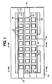
- a plurality of photosensors 10 are formed on an insulating substrate 11, for example by conventional solid state fabrication techniques, such as thin film techniques.
- the photosensors 10 define three separate parallel rows 15, 16, 17 of sensors.
- the individual sensors are connected in conventional manner to terminals (not illustrated) available for external interconnection of the device, for example via conductive layers (not illustrated) on the substrate.
- the device is lithographically processed to form pattern spacer strips 20, 21 between the photosensor rows 15, 16 and 16, 17, as well as pattern spacer strips 22, 23 outwardly of the rows 15 and 17.
- These spacers may be formed as a part of a conventional passivation step.
- the spacer 23 is provided with a central gap 24.
- the spacers 20-23 support a transparent cover sheet 25, such as glass, in a plane spaced from the substrate and photosensors 10.
- the periphery of the cover sheet 25 is bonded and sealed to the substrate by a layer 26 of a conventional liquid sealing material extending between the substrate and cover sheet, outwardly of the spacers 20-23.
- the sealing layer 26 extends around the periphery of the device, except for a port or opening 30 aligned with the row 15, a port or opening 31 aligned with the row 16, and a port or opening 32 extending to the gap 24 between the end portions of the spacer 23.
- the sealing layer extends to the spacers at the respective openings, so that the photosensors in row 15 are in a sealed channel open at the opening 30, the photosensors in row 16 are in a sealed channel open at the opening 31, and the photosensors in row 17 are in a sealed channel open at the opening 32.
- the openings 30 and 31 be provided at opposite ends of the device, to facilitate the filling of these two channels with a color medium.
- the channels are preferably initially evacuated, to permit the "vacuum" to draw color media fluids into the channels, in a manner similar to that used in the application of liquid crystal material to display panels.
- an opening in the sealing material such as the opening 32
- a valve 41 to permit the respective channel to be evacuated.
- the valve 41 is closed and a valve 42 is opened, to permit the "vacuum" in the channel to draw in colored liquid from a supply 43 of colored liquid.
- the channel is sealed by a conventional liquid sealing material 50, as illustrated in Fig. 4.
- the above described technique is only exemplary, and that any conventional technique may be employed to evacuate the channels so that a colored liquid may be drawn thereinto by the resultant vacuum.
- the device may be placed in a chamber, and the chamber then evacuated.
- each of the openings in the device is then brought into contact with a separate one of three sources of colored fluid.
- the liquid, i.e. flowable, color media may be any of various materials.
- UV curable epoxy dyes may be employed, and cured after filling in the device, in order to improve the mechanical stability of the device.
- colored gels may be employed in order to provide better color fidelity.
- Such materials provide superior matching to sensor performance, as compared with existing colored polyimides.
- the invention thereby provides an improved technique for producing a color scanner, that not only simplifies the fabrication of the scanner, but also readily permits the use of better color filter materials.
- the resultant color scanner device thereby is more readily adaptable to sensing of the desired colors.
- the device may be a thin-film device, formed by thin-film techniques, and having dimensions of the order of micrometers.
Description
- This invention relates to a method for producing a color scanning device, and to a color scanning device produced by the method.
- It is frequently desired to provide signals corresponding to the colors of an image, for example in color television systems, color reproduction systems, etc. For this purpose, it is necessary to provide a light scanning arrangement that is sensitive to different colors. In one technique for producing such signals, a sensing array is provided having a plurality of light sensing devices, such as photodiodes, arranged to intercept light, for example from scanning optics. Different colored optical filters are arranged in the optical path of the light to the different sensors, so that the output of each sensor is responsive to light of a different color.
- In the production of one form of color scanning device, as disclosed for example in US-A-5,053,298, photodiode arrays are deposited in recesses in a substrate, and covered with a transparent planarizing layer. After a pattern conforming to predetermined ones of the diode arrays is lithographically formed on the surface of the planarizing layer, the planarizing layer is covered with a coloring agent to cover the pattern. The coloring agent is then removed from the surface of the planarizing layer, a protective layer is provided on the colored pattern, and the process is repeated to form other patterns of different color.
- The above described process involves a number of photolithographic steps, and the precise alignment of the patterns with the respective diode arrays.
- In another method for producing a color scanning device, as disclosed in US-A-5,042,920, resin inks of different colors are printed on a transparent substrate in the form of patterns, such as stripes. In this process, the color patterns are overcoated with transparent electrodes of the same pattern. Pixel electrodes are formed on a second transparent substrate, and a sandwich is formed of these substrate assemblies, with a liquid crystal layer between the pattern electrodes and the pixel electrodes.
- In each of the above techniques for providing color filters for a light scanning devices, the coloring agents are thus applied to external surfaces of the device, which are covered in the final preparation of the device, and the provision of the color filters is relatively complicated and costly.
- Liquid color filters have been suggested for use in light sources, wherein color liquids are provided between glass plates, as disclosed e.g. in "Measuring Colour", R.W.G. Hunt, John Wiley & Sons, New York, 1987, pp 110-112, and "Redetermination of CIE Standard Source C'', F.W. Billmeyer, Jr., Color research and applications, Volume 8. No. 2, Summer 1983, pp 90-96. These references are directed to devices of macroscopic dimensions (e.g. centimeters) wherein the absorption coefficients of the color liquids are low, for example 1000 times too low to provide effective color filtering in devices of microscopic dimensions, (e.g. of the order of micrometers) such as thin-film scan arrays.
- The present invention is therefore directed to the provision of an improved color scanner device and method for fabricating the device.
- Briefly stated, in accordance with the invention, a color scanner has an array of a plurality of spaced apart photosensors arranged on a substrate. The array is separated into a plurality of regions by spacers, and a transparent cover sheet is sealed to the top of the device, so that the spacers space the cover sheet from the substrate and photosensors. The array may be formed by conventional thin-film techniques. The separate regions of the substrate are initially open, at at least one location, to permit evacuation of the respective region. Following evacuation of a region, it is contacted with a flowable liquid color medium, such as a dye, to permit the "vacuum" within the region to draw in the liquid color medium.
- The invention thereby enables the various regions of the device to be filled with a color medium in a simple an inexpensive manner, and also readily permits the use of color media that have desired color filter characteristics.
- In one embodiment of the invention, a plurality of rows of photosensors are formed on a substrate, and spacers are lithographically formed on the substrate to separate the rows. A transparent cover sheet, for example of glass, is sealed to the top of the device, while leaving an opening leading to each of the rows. In order to apply different color filters to the different rows, each of the rows is evacuated, and the device is positioned to permit the "vacuum" in each channel to draw in a different colored liquid or gel.
- In order that the invention may be more clearly understood, an embodiment will now be disclosed in greater detail with reference to the accompanying drawing, wherein:
- Fig. 1 is a top view of a color scanner device in accordance with the invention, without the cover sheet thereon, prior to filling of the device with color media;
- Fig. 2 is a cross sectional view of the color scanner device of Fig. 1, taken along the line 2-2 of Fig. 1, and including the cover sheet;
- Fig. 3 is a cross sectional view of the color scanner array of Fig. 1 taken along the line 3-3 of Fig. 1, and illustrating one technique for introducing flowable media into the array; and
- Fig. 4 is a top view of a color scanner device in accordance with the invention following sealing of the photosensor channels.
- In accordance with one embodiment of the invention, as illustrated in Figs. 1 and 2, a plurality of
photosensors 10 are formed on aninsulating substrate 11, for example by conventional solid state fabrication techniques, such as thin film techniques. In the illustrated embodiment, thephotosensors 10 define three separateparallel rows - In addition, the device is lithographically processed to form
pattern spacer strips photosensor rows pattern spacer strips rows spacer 23 is provided with acentral gap 24. The spacers 20-23 support atransparent cover sheet 25, such as glass, in a plane spaced from the substrate andphotosensors 10. The periphery of thecover sheet 25 is bonded and sealed to the substrate by alayer 26 of a conventional liquid sealing material extending between the substrate and cover sheet, outwardly of the spacers 20-23. - As illustrated in Fig. 1, the
sealing layer 26 extends around the periphery of the device, except for a port or opening 30 aligned with therow 15, a port or opening 31 aligned with therow 16, and a port or opening 32 extending to thegap 24 between the end portions of thespacer 23. The sealing layer extends to the spacers at the respective openings, so that the photosensors inrow 15 are in a sealed channel open at theopening 30, the photosensors inrow 16 are in a sealed channel open at theopening 31, and the photosensors inrow 17 are in a sealed channel open at the opening 32. As illustrated, it is preferred that theopenings - In order to provide a color medium in the channels, to thereby filter the light directed to the
photosensors 10 via thetransparent cover sheet 25, the channels are preferably initially evacuated, to permit the "vacuum" to draw color media fluids into the channels, in a manner similar to that used in the application of liquid crystal material to display panels. - For example, as illustrated in Fig. 3, an opening in the sealing material, such as the
opening 32, may be coupled to apump 40 via avalve 41, to permit the respective channel to be evacuated. After evacuation, thevalve 41 is closed and avalve 42 is opened, to permit the "vacuum" in the channel to draw in colored liquid from asupply 43 of colored liquid. After the colored liquid has been drawn into the channel, the channel is sealed by a conventionalliquid sealing material 50, as illustrated in Fig. 4. - It is of course apparent that the above described technique is only exemplary, and that any conventional technique may be employed to evacuate the channels so that a colored liquid may be drawn thereinto by the resultant vacuum. For example, the device may be placed in a chamber, and the chamber then evacuated. In this technique, each of the openings in the device is then brought into contact with a separate one of three sources of colored fluid.
- The liquid, i.e. flowable, color media may be any of various materials. For example, UV curable epoxy dyes may be employed, and cured after filling in the device, in order to improve the mechanical stability of the device. Alternatively, colored gels may be employed in order to provide better color fidelity. Such materials provide superior matching to sensor performance, as compared with existing colored polyimides.
- The invention thereby provides an improved technique for producing a color scanner, that not only simplifies the fabrication of the scanner, but also readily permits the use of better color filter materials. The resultant color scanner device thereby is more readily adaptable to sensing of the desired colors. The device may be a thin-film device, formed by thin-film techniques, and having dimensions of the order of micrometers.
Claims (11)
- A method for producing a color scanner, comprising forming a photosensor (10) on a substrate (11), and positioning a transparent cover sheet (25) spaced from said substrate and photosensor, characterised by sealing (21,23) said cover sheet to said substrate to define a chamber enclosing said photosensor, with said chamber having an opening (32), evacuating (40,41) said chamber, and then contacting (42,43) a flowable color medium with said opening, whereby the medium is drawn into said chamber through said opening.
- The method of claim 1 wherein said step of forming a photosensor (10) on a substrate comprises forming a photosensor on a substrate by thin-film techniques.
- The method of claim 1 comprising forming a plurality of spaced photosensor arrays (15,16,17) on a substrate (11), partially surrounding each of said arrays of sensors with spacers (20,21,22,23) extending from said substrate to form a separate channel for each array, with each channel having an open port (30,31,32), sealingly covering said channels with a layer of a transparent material (25) spaced from said substrate and photosensor arrays, evacuating (40,41) said channels, and contacting (42,43) the port of each of said channels with a flowable color medium, whereby the flowable color media are drawn into the respective channels.
- The method of claim 3 further comprising sealing (50) said ports after the flowable color medium has been drawn into the respective channel.
- The method of claim 3 or claim 4 wherein said step of contacting the port of each of said channels with a flowable color medium comprises contacting each port with a different colored liquid medium.
- The method of any one of claims 3 to 5 wherein said step of contacting the port of each of said channels with a flowable color medium comprises contacting each port with a different colored UV curable epoxy, and further comprising curing said UV curable epoxy after it has been drawn into the respective channels.
- A color scanning array comprising a substrate (11), and a plurality of spaced apart photosensor arrays (15,16,17) each comprising discrete photosensitive devices on said substrate, characterised by spacers (20,21,22,23,) separating said arrays into respective channels each having a port (30,31,32), a transparent layer (25) supported on said spacers and sealed by said spacers to said substrate, and different colored flowable color media filling different ones of said channels and located between all of the photosensitive devices and the transparent layer.
- The color scanning array of claim 7 wherein said flowable color media are colored gels.
- The color scanning array of claim 7 wherein said photosensor arrays comprise thin-film arrays.
- A color scanning array comprising a substrate (11), and a plurality of spaced apart photosensor arrays (15,16,17) each comprising discrete photosensitive devices on said substrate, characterised by spacers (20,21,22,23) separating said arrays into respective channels each having a port (30,31,32), a transparent layer (25) supported on said spacers and sealed by said spacers to said substrate, and different colored cured epoxy materials filling different ones of said channels and located between all of the photosensitive devices in each channel and the transparent layer (25).
- A color-scanning array as claimed in claim 10, wherein the channels have dimensions of the order of micrometers.
Applications Claiming Priority (2)
| Application Number | Priority Date | Filing Date | Title |
|---|---|---|---|
| US07/810,654 US5229595A (en) | 1991-12-19 | 1991-12-19 | Fluid-filled color filtered input scanner arrays |
| US810654 | 1991-12-19 |
Publications (2)
| Publication Number | Publication Date |
|---|---|
| EP0547839A1 EP0547839A1 (en) | 1993-06-23 |
| EP0547839B1 true EP0547839B1 (en) | 1997-04-02 |
Family
ID=25204355
Family Applications (1)
| Application Number | Title | Priority Date | Filing Date |
|---|---|---|---|
| EP92311291A Expired - Lifetime EP0547839B1 (en) | 1991-12-19 | 1992-12-10 | Color scanning device and method for producing the device |
Country Status (4)
| Country | Link |
|---|---|
| US (1) | US5229595A (en) |
| EP (1) | EP0547839B1 (en) |
| JP (1) | JP3270778B2 (en) |
| DE (1) | DE69218738T2 (en) |
Families Citing this family (6)
| Publication number | Priority date | Publication date | Assignee | Title |
|---|---|---|---|---|
| DE69514874T2 (en) * | 1994-08-23 | 2000-07-20 | Hewlett Packard Co | Sensor arrangement for an optical image scanner which supplies gray value and color signals |
| US5750982A (en) * | 1996-04-16 | 1998-05-12 | Eastman Kodak Company | Method of mounting filters on image sensors |
| TW377517B (en) * | 1998-03-19 | 1999-12-21 | United Microelectronics Corp | Color sensing apparatus of diode and the method of manufacturing the same |
| US20090086064A1 (en) * | 2007-09-27 | 2009-04-02 | Micron Technology, Inc. | Dynamic adaptive color filter array |
| JP5747556B2 (en) * | 2011-02-25 | 2015-07-15 | セイコーエプソン株式会社 | Magnetic field measuring apparatus and cell array |
| EP3640987A4 (en) * | 2017-06-15 | 2021-04-28 | Nikon Corporation | Imaging element, imaging device and imaging method |
Family Cites Families (30)
| Publication number | Priority date | Publication date | Assignee | Title |
|---|---|---|---|---|
| CH556625A (en) * | 1972-09-06 | 1974-11-29 | Siemens Ag | SINGLE TUBE COLOR TELEVISION CAMERA WITH COLOR STRIPED FILTERS. |
| JPS50147339A (en) * | 1974-05-16 | 1975-11-26 | ||
| US4081277A (en) * | 1976-10-08 | 1978-03-28 | Eastman Kodak Company | Method for making a solid-state color imaging device having an integral color filter and the device |
| US4204866A (en) * | 1976-10-08 | 1980-05-27 | Eastman Kodak Company | Solid-state color imaging devices and method for making them |
| US4093352A (en) * | 1977-03-17 | 1978-06-06 | Pisar Robert J | Window adapted to be flooded with liquid |
| US4149091A (en) * | 1977-05-02 | 1979-04-10 | Xerox Corporation | Scanning apparatus |
| US4092632A (en) * | 1977-05-02 | 1978-05-30 | Xerox Corporation | Crossover arrangement for multiple scanning arrays |
| US4146786A (en) * | 1977-05-02 | 1979-03-27 | Xerox Corporation | Scanner with modular array of photocells |
| US4122352A (en) * | 1977-05-02 | 1978-10-24 | Xerox Corporation | Scanning array configuration |
| US4386143A (en) * | 1978-06-28 | 1983-05-31 | Masamichi Sato | Multicolor optical filters and process for producing the same |
| JPS5694309A (en) * | 1979-12-27 | 1981-07-30 | Fuji Photo Film Co Ltd | Multicolor optical filter and its production |
| DE3004717C2 (en) * | 1980-02-08 | 1986-03-27 | Agfa-Gevaert Ag, 5090 Leverkusen | Device for the electronic scanning of objects to be recorded |
| US4523102A (en) * | 1980-03-17 | 1985-06-11 | Matsushita Electric Industrial Co., Ltd. | Solid-state color-image sensor and process for fabricating the same |
| NL8105071A (en) * | 1981-11-10 | 1983-06-01 | Philips Nv | COLOR IMAGE RECORDING DEVICE. |
| JPS5984206A (en) * | 1982-11-08 | 1984-05-15 | Seiko Epson Corp | Color filter |
| US4667092A (en) * | 1982-12-28 | 1987-05-19 | Nec Corporation | Solid-state image device with resin lens and resin contact layer |
| JPS59124768A (en) * | 1982-12-29 | 1984-07-18 | Fujitsu Ltd | Nonvolatile semiconductor memory device and its manufacture |
| JPS6073601A (en) * | 1983-09-30 | 1985-04-25 | Nec Corp | Solid-state image pickup element |
| JPS6125358A (en) * | 1984-07-13 | 1986-02-04 | Matsushita Electric Ind Co Ltd | Photoelectric converter |
| JPS6152061A (en) * | 1984-08-22 | 1986-03-14 | Toshiba Corp | Close-adhering-type color image sensor |
| US4827118A (en) * | 1986-07-10 | 1989-05-02 | Minolta Camera Kabushiki Kaisha | Light-sensitive device having color filter and manufacturing method thereof |
| US4725889A (en) * | 1986-07-15 | 1988-02-16 | Ovonic Imaging Systems, Inc. | Photosensitive line imager utilizing a movable scanning arm |
| US4728803A (en) * | 1986-07-15 | 1988-03-01 | Ovonic Imaging Systems, Inc. | Signal processing apparatus and method for photosensitive imaging system |
| US4739414A (en) * | 1986-07-15 | 1988-04-19 | Ovonic Imaging Systems, Inc. | Large area array of thin film photosensitive elements for image detection |
| JPH01154102A (en) * | 1987-12-11 | 1989-06-16 | Fuji Photo Film Co Ltd | Interference filter |
| DE8808558U1 (en) * | 1988-07-04 | 1988-08-18 | Hermann Hirsch Leder- Und Kunststoffwarenfabrik, Klagenfurt, Kaernten, At | |
| DE68920702T2 (en) * | 1988-11-10 | 1995-06-14 | Toshiba Kawasaki Kk | Liquid crystal display device, color filter therefor, and method of manufacturing the color filter. |
| DE3911359A1 (en) * | 1989-04-07 | 1990-10-11 | Nokia Unterhaltungselektronik | METHOD FOR FILLING A LIQUID CRYSTAL CELL |
| KR920005444B1 (en) * | 1989-12-02 | 1992-07-04 | 삼성전자 주식회사 | Method of manufacturing color filter |
| JPH03280002A (en) * | 1990-03-29 | 1991-12-11 | Toppan Printing Co Ltd | Color filter |
-
1991
- 1991-12-19 US US07/810,654 patent/US5229595A/en not_active Expired - Lifetime
-
1992
- 1992-12-09 JP JP35201892A patent/JP3270778B2/en not_active Expired - Lifetime
- 1992-12-10 DE DE69218738T patent/DE69218738T2/en not_active Expired - Lifetime
- 1992-12-10 EP EP92311291A patent/EP0547839B1/en not_active Expired - Lifetime
Also Published As
| Publication number | Publication date |
|---|---|
| DE69218738T2 (en) | 1997-09-11 |
| JPH05267631A (en) | 1993-10-15 |
| DE69218738D1 (en) | 1997-05-07 |
| JP3270778B2 (en) | 2002-04-02 |
| EP0547839A1 (en) | 1993-06-23 |
| US5229595A (en) | 1993-07-20 |
Similar Documents
| Publication | Publication Date | Title |
|---|---|---|
| US5486708A (en) | Light valve device using semiconductive composite substrate | |
| US5480582A (en) | Process for synthesizing amorphous silica microspheres with fluorescence behavior | |
| KR100773216B1 (en) | Substrate apparatus | |
| JPH09172154A (en) | Flat color filter arrangement for ccd with embedded color filter element | |
| WO2002054499A2 (en) | Infrared detector packaged with improved antireflection element | |
| EP0547839B1 (en) | Color scanning device and method for producing the device | |
| US20050190311A1 (en) | Liquid crystal display device | |
| JPS56140324A (en) | Display device | |
| CN112071969A (en) | Quantum dot flexible LED display device and preparation method thereof | |
| US5074683A (en) | Fiber optic faceplates and method of mounting same | |
| JPS613122A (en) | Production of liquid crystal color display element | |
| KR20000068562A (en) | Substrates for large area electronic devices | |
| KR20040012303A (en) | a panel for a liquid crystal display, a liquid crystal display including the panel, and a methods for manufacturing the same | |
| GB2269910A (en) | Liquid crystal cell cluster | |
| US6400431B1 (en) | Liquid crystal display element | |
| JPS613123A (en) | Production of liquid crystal color display element | |
| JPH02298916A (en) | Liquid crystal display device | |
| JP3975753B2 (en) | Optical cell | |
| KR101338999B1 (en) | Electrophoretic display device and method of fabricating thereof | |
| JP3012100B2 (en) | Method for manufacturing solid-state imaging device | |
| JPH03192334A (en) | Liquid crystal display panel | |
| CN114690301A (en) | Multispectral optical filter, preparation method thereof and image acquisition device | |
| JPS6262331A (en) | Manufacture of liquid crystal display unit | |
| JPS62262001A (en) | Solid-state color image pickup device | |
| JPH08313920A (en) | Production of color liquid crystal device |
Legal Events
| Date | Code | Title | Description |
|---|---|---|---|
| PUAI | Public reference made under article 153(3) epc to a published international application that has entered the european phase |
Free format text: ORIGINAL CODE: 0009012 |
|
| AK | Designated contracting states |
Kind code of ref document: A1 Designated state(s): DE FR GB |
|
| 17P | Request for examination filed |
Effective date: 19931208 |
|
| 17Q | First examination report despatched |
Effective date: 19951201 |
|
| GRAG | Despatch of communication of intention to grant |
Free format text: ORIGINAL CODE: EPIDOS AGRA |
|
| GRAH | Despatch of communication of intention to grant a patent |
Free format text: ORIGINAL CODE: EPIDOS IGRA |
|
| GRAH | Despatch of communication of intention to grant a patent |
Free format text: ORIGINAL CODE: EPIDOS IGRA |
|
| GRAA | (expected) grant |
Free format text: ORIGINAL CODE: 0009210 |
|
| AK | Designated contracting states |
Kind code of ref document: B1 Designated state(s): DE FR GB |
|
| REF | Corresponds to: |
Ref document number: 69218738 Country of ref document: DE Date of ref document: 19970507 |
|
| ET | Fr: translation filed | ||
| PLBE | No opposition filed within time limit |
Free format text: ORIGINAL CODE: 0009261 |
|
| STAA | Information on the status of an ep patent application or granted ep patent |
Free format text: STATUS: NO OPPOSITION FILED WITHIN TIME LIMIT |
|
| 26N | No opposition filed | ||
| REG | Reference to a national code |
Ref country code: GB Ref legal event code: IF02 |
|
| PGFP | Annual fee paid to national office [announced via postgrant information from national office to epo] |
Ref country code: GB Payment date: 20101208 Year of fee payment: 19 |
|
| PGFP | Annual fee paid to national office [announced via postgrant information from national office to epo] |
Ref country code: DE Payment date: 20101208 Year of fee payment: 19 |
|
| PGFP | Annual fee paid to national office [announced via postgrant information from national office to epo] |
Ref country code: FR Payment date: 20111219 Year of fee payment: 20 |
|
| REG | Reference to a national code |
Ref country code: DE Ref legal event code: R071 Ref document number: 69218738 Country of ref document: DE |
|
| REG | Reference to a national code |
Ref country code: DE Ref legal event code: R071 Ref document number: 69218738 Country of ref document: DE |
|
| REG | Reference to a national code |
Ref country code: GB Ref legal event code: PE20 Expiry date: 20121209 |
|
| PG25 | Lapsed in a contracting state [announced via postgrant information from national office to epo] |
Ref country code: GB Free format text: LAPSE BECAUSE OF EXPIRATION OF PROTECTION Effective date: 20121209 |