EP0545263A2 - Method of forming trench isolation having polishing step and method of manufacturing semiconductor device - Google Patents
Method of forming trench isolation having polishing step and method of manufacturing semiconductor device Download PDFInfo
- Publication number
- EP0545263A2 EP0545263A2 EP92120116A EP92120116A EP0545263A2 EP 0545263 A2 EP0545263 A2 EP 0545263A2 EP 92120116 A EP92120116 A EP 92120116A EP 92120116 A EP92120116 A EP 92120116A EP 0545263 A2 EP0545263 A2 EP 0545263A2
- Authority
- EP
- European Patent Office
- Prior art keywords
- polishing
- burying
- etching
- burying material
- forming
- Prior art date
- Legal status (The legal status is an assumption and is not a legal conclusion. Google has not performed a legal analysis and makes no representation as to the accuracy of the status listed.)
- Granted
Links
Images


Classifications
-
- H—ELECTRICITY
- H01—ELECTRIC ELEMENTS
- H01L—SEMICONDUCTOR DEVICES NOT COVERED BY CLASS H10
- H01L21/00—Processes or apparatus adapted for the manufacture or treatment of semiconductor or solid state devices or of parts thereof
- H01L21/02—Manufacture or treatment of semiconductor devices or of parts thereof
- H01L21/02104—Forming layers
- H01L21/02107—Forming insulating materials on a substrate
- H01L21/02109—Forming insulating materials on a substrate characterised by the type of layer, e.g. type of material, porous/non-porous, pre-cursors, mixtures or laminates
- H01L21/02112—Forming insulating materials on a substrate characterised by the type of layer, e.g. type of material, porous/non-porous, pre-cursors, mixtures or laminates characterised by the material of the layer
- H01L21/02123—Forming insulating materials on a substrate characterised by the type of layer, e.g. type of material, porous/non-porous, pre-cursors, mixtures or laminates characterised by the material of the layer the material containing silicon
- H01L21/02164—Forming insulating materials on a substrate characterised by the type of layer, e.g. type of material, porous/non-porous, pre-cursors, mixtures or laminates characterised by the material of the layer the material containing silicon the material being a silicon oxide, e.g. SiO2
-
- H—ELECTRICITY
- H01—ELECTRIC ELEMENTS
- H01L—SEMICONDUCTOR DEVICES NOT COVERED BY CLASS H10
- H01L21/00—Processes or apparatus adapted for the manufacture or treatment of semiconductor or solid state devices or of parts thereof
- H01L21/02—Manufacture or treatment of semiconductor devices or of parts thereof
- H01L21/02104—Forming layers
- H01L21/02107—Forming insulating materials on a substrate
- H01L21/02109—Forming insulating materials on a substrate characterised by the type of layer, e.g. type of material, porous/non-porous, pre-cursors, mixtures or laminates
- H01L21/02205—Forming insulating materials on a substrate characterised by the type of layer, e.g. type of material, porous/non-porous, pre-cursors, mixtures or laminates the layer being characterised by the precursor material for deposition
- H01L21/02208—Forming insulating materials on a substrate characterised by the type of layer, e.g. type of material, porous/non-porous, pre-cursors, mixtures or laminates the layer being characterised by the precursor material for deposition the precursor containing a compound comprising Si
- H01L21/02214—Forming insulating materials on a substrate characterised by the type of layer, e.g. type of material, porous/non-porous, pre-cursors, mixtures or laminates the layer being characterised by the precursor material for deposition the precursor containing a compound comprising Si the compound comprising silicon and oxygen
- H01L21/02216—Forming insulating materials on a substrate characterised by the type of layer, e.g. type of material, porous/non-porous, pre-cursors, mixtures or laminates the layer being characterised by the precursor material for deposition the precursor containing a compound comprising Si the compound comprising silicon and oxygen the compound being a molecule comprising at least one silicon-oxygen bond and the compound having hydrogen or an organic group attached to the silicon or oxygen, e.g. a siloxane
-
- H—ELECTRICITY
- H01—ELECTRIC ELEMENTS
- H01L—SEMICONDUCTOR DEVICES NOT COVERED BY CLASS H10
- H01L21/00—Processes or apparatus adapted for the manufacture or treatment of semiconductor or solid state devices or of parts thereof
- H01L21/02—Manufacture or treatment of semiconductor devices or of parts thereof
- H01L21/02104—Forming layers
- H01L21/02107—Forming insulating materials on a substrate
- H01L21/02225—Forming insulating materials on a substrate characterised by the process for the formation of the insulating layer
- H01L21/0226—Forming insulating materials on a substrate characterised by the process for the formation of the insulating layer formation by a deposition process
- H01L21/02263—Forming insulating materials on a substrate characterised by the process for the formation of the insulating layer formation by a deposition process deposition from the gas or vapour phase
- H01L21/02271—Forming insulating materials on a substrate characterised by the process for the formation of the insulating layer formation by a deposition process deposition from the gas or vapour phase deposition by decomposition or reaction of gaseous or vapour phase compounds, i.e. chemical vapour deposition
-
- H—ELECTRICITY
- H01—ELECTRIC ELEMENTS
- H01L—SEMICONDUCTOR DEVICES NOT COVERED BY CLASS H10
- H01L21/00—Processes or apparatus adapted for the manufacture or treatment of semiconductor or solid state devices or of parts thereof
- H01L21/02—Manufacture or treatment of semiconductor devices or of parts thereof
- H01L21/04—Manufacture or treatment of semiconductor devices or of parts thereof the devices having at least one potential-jump barrier or surface barrier, e.g. PN junction, depletion layer or carrier concentration layer
- H01L21/18—Manufacture or treatment of semiconductor devices or of parts thereof the devices having at least one potential-jump barrier or surface barrier, e.g. PN junction, depletion layer or carrier concentration layer the devices having semiconductor bodies comprising elements of Group IV of the Periodic System or AIIIBV compounds with or without impurities, e.g. doping materials
- H01L21/30—Treatment of semiconductor bodies using processes or apparatus not provided for in groups H01L21/20 - H01L21/26
- H01L21/302—Treatment of semiconductor bodies using processes or apparatus not provided for in groups H01L21/20 - H01L21/26 to change their surface-physical characteristics or shape, e.g. etching, polishing, cutting
- H01L21/306—Chemical or electrical treatment, e.g. electrolytic etching
- H01L21/3065—Plasma etching; Reactive-ion etching
-
- H—ELECTRICITY
- H01—ELECTRIC ELEMENTS
- H01L—SEMICONDUCTOR DEVICES NOT COVERED BY CLASS H10
- H01L21/00—Processes or apparatus adapted for the manufacture or treatment of semiconductor or solid state devices or of parts thereof
- H01L21/02—Manufacture or treatment of semiconductor devices or of parts thereof
- H01L21/04—Manufacture or treatment of semiconductor devices or of parts thereof the devices having at least one potential-jump barrier or surface barrier, e.g. PN junction, depletion layer or carrier concentration layer
- H01L21/18—Manufacture or treatment of semiconductor devices or of parts thereof the devices having at least one potential-jump barrier or surface barrier, e.g. PN junction, depletion layer or carrier concentration layer the devices having semiconductor bodies comprising elements of Group IV of the Periodic System or AIIIBV compounds with or without impurities, e.g. doping materials
- H01L21/30—Treatment of semiconductor bodies using processes or apparatus not provided for in groups H01L21/20 - H01L21/26
- H01L21/31—Treatment of semiconductor bodies using processes or apparatus not provided for in groups H01L21/20 - H01L21/26 to form insulating layers thereon, e.g. for masking or by using photolithographic techniques; After treatment of these layers; Selection of materials for these layers
- H01L21/3105—After-treatment
- H01L21/31051—Planarisation of the insulating layers
- H01L21/31053—Planarisation of the insulating layers involving a dielectric removal step
- H01L21/31055—Planarisation of the insulating layers involving a dielectric removal step the removal being a chemical etching step, e.g. dry etching
-
- H—ELECTRICITY
- H01—ELECTRIC ELEMENTS
- H01L—SEMICONDUCTOR DEVICES NOT COVERED BY CLASS H10
- H01L21/00—Processes or apparatus adapted for the manufacture or treatment of semiconductor or solid state devices or of parts thereof
- H01L21/02—Manufacture or treatment of semiconductor devices or of parts thereof
- H01L21/04—Manufacture or treatment of semiconductor devices or of parts thereof the devices having at least one potential-jump barrier or surface barrier, e.g. PN junction, depletion layer or carrier concentration layer
- H01L21/18—Manufacture or treatment of semiconductor devices or of parts thereof the devices having at least one potential-jump barrier or surface barrier, e.g. PN junction, depletion layer or carrier concentration layer the devices having semiconductor bodies comprising elements of Group IV of the Periodic System or AIIIBV compounds with or without impurities, e.g. doping materials
- H01L21/30—Treatment of semiconductor bodies using processes or apparatus not provided for in groups H01L21/20 - H01L21/26
- H01L21/31—Treatment of semiconductor bodies using processes or apparatus not provided for in groups H01L21/20 - H01L21/26 to form insulating layers thereon, e.g. for masking or by using photolithographic techniques; After treatment of these layers; Selection of materials for these layers
- H01L21/3105—After-treatment
- H01L21/311—Etching the insulating layers by chemical or physical means
- H01L21/31105—Etching inorganic layers
- H01L21/31111—Etching inorganic layers by chemical means
- H01L21/31116—Etching inorganic layers by chemical means by dry-etching
-
- H—ELECTRICITY
- H01—ELECTRIC ELEMENTS
- H01L—SEMICONDUCTOR DEVICES NOT COVERED BY CLASS H10
- H01L21/00—Processes or apparatus adapted for the manufacture or treatment of semiconductor or solid state devices or of parts thereof
- H01L21/02—Manufacture or treatment of semiconductor devices or of parts thereof
- H01L21/04—Manufacture or treatment of semiconductor devices or of parts thereof the devices having at least one potential-jump barrier or surface barrier, e.g. PN junction, depletion layer or carrier concentration layer
- H01L21/18—Manufacture or treatment of semiconductor devices or of parts thereof the devices having at least one potential-jump barrier or surface barrier, e.g. PN junction, depletion layer or carrier concentration layer the devices having semiconductor bodies comprising elements of Group IV of the Periodic System or AIIIBV compounds with or without impurities, e.g. doping materials
- H01L21/30—Treatment of semiconductor bodies using processes or apparatus not provided for in groups H01L21/20 - H01L21/26
- H01L21/31—Treatment of semiconductor bodies using processes or apparatus not provided for in groups H01L21/20 - H01L21/26 to form insulating layers thereon, e.g. for masking or by using photolithographic techniques; After treatment of these layers; Selection of materials for these layers
- H01L21/314—Inorganic layers
- H01L21/316—Inorganic layers composed of oxides or glassy oxides or oxide based glass
- H01L21/31604—Deposition from a gas or vapour
-
- H—ELECTRICITY
- H01—ELECTRIC ELEMENTS
- H01L—SEMICONDUCTOR DEVICES NOT COVERED BY CLASS H10
- H01L21/00—Processes or apparatus adapted for the manufacture or treatment of semiconductor or solid state devices or of parts thereof
- H01L21/70—Manufacture or treatment of devices consisting of a plurality of solid state components formed in or on a common substrate or of parts thereof; Manufacture of integrated circuit devices or of parts thereof
- H01L21/71—Manufacture of specific parts of devices defined in group H01L21/70
- H01L21/76—Making of isolation regions between components
- H01L21/762—Dielectric regions, e.g. EPIC dielectric isolation, LOCOS; Trench refilling techniques, SOI technology, use of channel stoppers
- H01L21/76224—Dielectric regions, e.g. EPIC dielectric isolation, LOCOS; Trench refilling techniques, SOI technology, use of channel stoppers using trench refilling with dielectric materials
- H01L21/76229—Concurrent filling of a plurality of trenches having a different trench shape or dimension, e.g. rectangular and V-shaped trenches, wide and narrow trenches, shallow and deep trenches
-
- H—ELECTRICITY
- H01—ELECTRIC ELEMENTS
- H01L—SEMICONDUCTOR DEVICES NOT COVERED BY CLASS H10
- H01L21/00—Processes or apparatus adapted for the manufacture or treatment of semiconductor or solid state devices or of parts thereof
- H01L21/02—Manufacture or treatment of semiconductor devices or of parts thereof
- H01L21/02104—Forming layers
- H01L21/02107—Forming insulating materials on a substrate
- H01L21/02109—Forming insulating materials on a substrate characterised by the type of layer, e.g. type of material, porous/non-porous, pre-cursors, mixtures or laminates
- H01L21/02112—Forming insulating materials on a substrate characterised by the type of layer, e.g. type of material, porous/non-porous, pre-cursors, mixtures or laminates characterised by the material of the layer
- H01L21/02123—Forming insulating materials on a substrate characterised by the type of layer, e.g. type of material, porous/non-porous, pre-cursors, mixtures or laminates characterised by the material of the layer the material containing silicon
- H01L21/0217—Forming insulating materials on a substrate characterised by the type of layer, e.g. type of material, porous/non-porous, pre-cursors, mixtures or laminates characterised by the material of the layer the material containing silicon the material being a silicon nitride not containing oxygen, e.g. SixNy or SixByNz
-
- Y—GENERAL TAGGING OF NEW TECHNOLOGICAL DEVELOPMENTS; GENERAL TAGGING OF CROSS-SECTIONAL TECHNOLOGIES SPANNING OVER SEVERAL SECTIONS OF THE IPC; TECHNICAL SUBJECTS COVERED BY FORMER USPC CROSS-REFERENCE ART COLLECTIONS [XRACs] AND DIGESTS
- Y10—TECHNICAL SUBJECTS COVERED BY FORMER USPC
- Y10S—TECHNICAL SUBJECTS COVERED BY FORMER USPC CROSS-REFERENCE ART COLLECTIONS [XRACs] AND DIGESTS
- Y10S438/00—Semiconductor device manufacturing: process
- Y10S438/97—Specified etch stop material
Definitions
- the present invention concerns a method of forming trench isolation having a polishing step and a method of manufacturing a semiconductor device having a polishing step.
- the present invention can be applied to the formation of trench isolation (trench type inter-device separation) in various kinds of electronic materials, a method of manufacturing various kinds of semiconductor devices having trench isolation, as well as a method of manufacturing various kinds of semiconductor devices having a recess burying step and a subsequent flattening and polishing step.
- a polishing step including a step of burying recesses defined with a plurality of protrusion patterns (that is, defined between each of protrusion patterns) by a burying material and a step of flattening the burying material formed on the protrusion patterns by polishing.
- the polishing technique has a wide application use and it can be utilized, for example, for flattening unevenness resulting in a substrate such as a semiconductor substrate upon manufacturing a semiconductor device (refer, for example, to Japanese Patent Laid Open sho 63-39835).
- the capacitance of a device has been increased in the field of semiconductor devices and various kinds of techniques have been developed in order to increase the capacitance while minimizing a chip area as small as possible and, for example, a multi-layered wiring technique is indispensable therefor.
- a multi-layered wiring technique it is extremely important to flatten the underlying substrate in order to prevent disconnection of the multi-layred wiring. This is because unevenness on the underlying substrate, if any, will lead to occurrence of wire disconnection on a step caused by the unevenness (so-called step disconnection). In order to flatten the underlying substrate satisfactorily, flattening from the initial stage is important.
- Trench isolation is a technique for inter-device isolation by burying an insulator to trenches formed on a semiconductor substrate and it is advantageous for higher degree integration since fine trenches can be formed.
- it is necessary to remove protrusions composed of a burying material deposited to the portions other than the trenches for attaining a flattened surface.
- the trench can be formed as a recess between two protrusion patterns but, when a burying material is buried in the recess (trench), since the burying material is also deposited on the protrusion patterns other than the trench to form a protruding portion, it has to be flattened.
- a method as shown in Fig. 11 has been known as a method of forming a flat trench isolation.
- a thin silicon oxide film 2 and a thin silicone nitride film 3 are formed on a semiconductor substrate 1, then trenches 41, 42 and 43 are formed by etching using a photolithographic step and, subsequently, an inner wall oxide film, that is, the silicon oxide layer 2 is formed by oxidation to provide a semiconductor substrate.
- a burying material 5 is deposited in the trenches 41-43 by a deposition means, for example, CVD to obtain a structure as shown in the figure.
- the burying material 5 is deposited to a large thickness also to the portions other than the trenches 42 - 43 to result in protrusions 51.
- the protrusions 51 are removed to flatten by polishing.
- a silicon nitride film 3 having a polishing speed lower than that may be used for instance as a stopper layer for polishing.
- Such a method is applied, in addition to the trench isolation process, also to other processes for forming flat interlayer insulation films such as formation of a trench capacitor accompanying trench burying, formation of trench contact (trench plug) or formation of a layer by a blanket W-CVD process.
- a block resist 31 is formed in the recess of CVD-SiO2 as the burying material 5, on which a resist coating film 3 is formed which are then etched back.
- a structure as shown in Fig. 13(b) is obtained.
- it is flattened by polishing to obtain a flattened structure as shown in Fig. 13(c).
- a patterning for the block resist is displaced to form a resist out of the recess as shown by reference numeral 31' in Fig.
- trenches 41 - 43 are formed as recesses between each of protrusion patterns 61 - 64.
- the protrusion patterns 61 - 64 function as a stopper upon polishing.
- the density of the protrusion pattern 61 is small or course in the portion A of the figure in which the protrusion pattern 61 is present.
- a ratio of the protrusion patterns in a unit area is great and, accordingly, the density of the protrusion pattern is large or dense.
- the area of the stopper layer 3 in the unit area is small and, accordingly, the density thereof is coarse in the illustrated portion A.
- the area of the stopper layer 3 in the unit area is large, the density of the polishing stopper 3 is dense in the illustrated portion B shown in the figure. If there is unevenness of the ratio of the polishing stopper layer 3 (which exists each for the protrusion patterns 61 - 64), polishing tends to become uneven.
- a polishing stopper layer For instance, in a peripheral circuit, if the area ratio per unit area of a protrusion pattern present there that function as a polishing stopper layer is low (for example, in a case of the region A in Fig. 14), since a polishing pressure is concentrated upon polishing to the protrusion pattern (stopper layer), the polishing rate is increased, so that mere selection ratio of the protrusion pattern (stopper layer) is insufficient and an isolation pattern 61 is scraped off as shown in Fig. 14(b) which no more provides an intended effect as the stopper layer. As a result, the region A is concaved and uniform and satisfactory flattening can not be attained as shown in Fig. 14(b).
- Another object of the present invention is to provide a method of manufacturing a semiconductor device having a polishing step of applying flattening after burying, wherein a satisfactory flattened shape can be formed even in a case where a distribution of a portion exhibiting the function of a polishing stopper on a portion to be polished has unevenness, also in a portion in which an area ratio of the stopper layer per unit area is low.
- the foregoing object can be attained by the present invention of claim 1, concerning a method of forming trench isolation including a burying step of burying trenches by a deposition means for conducting etching and deposition simultaneously and a polishing step of flattening a burying material by polishing, wherein the method comprises at least an isotropic etching step for isotropically etching the burying material before the polishing step.
- the present invention of claim 2 concerning a method of forming trench isolation as defined in claim 1, wherein trenches are formed in a structure which has an etching stopper layer comprising a three-layered structure, and in which the upper layer of the etching stopper layer comprises a film having a polishing rate smaller than that of the burying material and an etching rate also smaller than that of the burying material, an intermediate layer of the etching stopper layer comprises a film having an etching rate smaller than that of the upper layer and a lower layer of the etching stopper layer comprises a film having an etching rate smaller than that of the intermediate layer and greater than that of the substrate.
- the foregoing object can be attained by the present invention of claim 5, concerning a method of manufacturing a semiconductor device for forming trench isolation, which comprises a burying step of burying trenches by a bias ECR-CVD process, an isotropic etching step of isotropically etching a burying material thereby etching the burying material on a wide protrusion region and a polishing step of flattening the burying material by polishing.
- the foregoing object can be attained by the present invention of claim 6, concerning a method of manufacturing a semiconductor device for forming trench isolation by forming trenches in a structure, in which a substrate to form trench isolation has an etching stopper layer compri sing a three-layered structure, in which the upper layer of the etching stopper layer comprises silicon nitride, an intermediate layer of the etching stopper layer comprises polysilicon and a lower layer of the etching stopper layer comprises a silicon dioxide film.
- the foregoing object can be attained by the present invention of claim 7, concerning a method of manufacturing a semiconductor device having a polishing step including a step of burying recesses defined with a plurality of protrusion patterns by a burying material and a polishing step of flattening the burying material formed on the protrusion patterns by polishing, which comprises previously forming a pattern that constitutes a stopper layer for polishing and that is not intended directly for the function as a wiring or insulation portion, to a portion in which the density of the stopper layer for polishing is coarse.
- the foregoing object can be attained by the present invention of claim 8, concerning a method of manufacturing a semiconductor device having a polishing step as defined in claim 7, wherein the patterns by polishing, which comprises previously forming a pattern that constitutes a stopper layer for polishing and that is not intended directly for the function as a wiring or insulation portion is finally removed.
- the foregoing object can be attained by the present invention of claim 9, concerning a method of manufacturing a semiconductor device having a polishing step including a step of burying recesses defined with a plurality of protrusion patterns with a burying material on a semiconductor substrate having the plurality of protrusion patterns comprising a wide protrusion regions and narrow protrusion regions, and a step of flattening the burying material formed on the protrusion patterns by polishing, wherein the method comprises a step of previously forming a pattern that constitutes a stopper layer for polishing and that is finally removed to a portion in which the density of the stopper layer for polishing is coarse, and a step of at least partially etching the burying material on the wide protrusion regions prior to the flattening step by polishing.
- the foregoing object can be attained by the present invention of claim 10, concerning a method of manufacturing a semiconductor device in which a plurality of protrusion patterns are formed on a substrate and trenches comprising recesses defined therebetween are buried, wherein a pattern as a stopper layer for polishing is previously formed to a portion in which the density of the protrusion patterns formed with the stopper layer for polishing is coarse to obtain a structure having the protrusions being uniformly distributed, thereby making the area ratio of the stopper layer uniform, subsequently, burying material is deposited and then the burying material on the protrusion patterns and the previously formed patterns are removed by polishing to obtain a flattened structure.
- the present invention of claim 15 concerning a method of manufacturing a semiconductor device as defined in claim 9, wherein the layer constituting the polishing stopper comprises silicon nitride and a step of at least partially removing the burying material on the wide protrusion region prior to the flattening step by polishing utilizes a means of applying isotropic etching while masking other positions than the etched portion with a resist.
- the foregoing object can be attained by the present invention of claim 16, concerning a method of manufacturing a semiconductor device including a burying step for forming a recess burying material by a deposition means on a substrate formed with a plurality of recesses and a polishing step of flattening the burying material by polishing, wherein the method comprises a resist forming step of forming a resist on the substrate after the polishing step, a resist pattern forming step of forming a resist pattern while exposing the burying material remaining in the portions other than the recesses to be buried, and a removing step of removing the burying material remaining in the portions other than the recesses to be buried by using the resist pattern as a mask.
- the foregoing object can be attained by the present invention of claim 17, concerning a method of manufacturing a semiconductor device including a burying step for forming recess burying material by a deposition means on a substrate formed with a plurality of recesses and a polishing step of flattening the burying material by polishing, wherein the method comprises a flattened layer forming step of forming a flattened layer on the substrate, and an etching back step for etching back under the condition in which an etching rate is equal between the flattened layer and the burying material.
- the foregoing object can be attained by the present invention of claim 18, concerning a method of manufacturing a semiconductor device which comprises burying silicon dioxide as a burying material into a plurality of recesses on a substrate having a silicon nitride film as a stopper layer for polishing by a base CR-CVD process and then conducting a polishing step of flattening the burying material by polishing, conducting a resist forming step of forming a resist on a substrate after the polishing step and a resist pattern forming step of forming a resist pattern while exposing the burying material remaining in the portion other than recesses to be buried as the burying material not removed completely and, subsequently, conducting a removing step of removing the burying material remaining in the portion other than the recesses to be buried by using the resist pattern as a mask, thereby conducting burying and flattening with no residue of the burying material not removed completely.
- the foregoing object can be attained by the present invention of claim 19, concerning a method of manufacturing a semiconductor device which comprises a burying step of forming a recess burying material by depositing silicon dioxide by a bias ECR-CVD process on a substrate in which a plurality of recesses are formed and a silicon nitride film is formed as a stopper layer for polishing stopper, a polishing step of flattening the burying material by polishing, a flattened layer forming step of forming a flattened layer on a substrate by a resist or SOG and an etching back step of applying etching back in a condition in which an etching rate is made equal between the flattened layer and the burying material.
- the foregoing object can be attained by the present invention of claim 20, concerning a method of manufacturing a semiconductor device having a polishing step including a step of forming a plurality of protrusion patterns each having a stopper layer for polishing in the upper portion, a step of burying recesses defined with a plurality of protrusion patterns by a burying material and a step of flattening the burying material formed on the protrusion patterns by polishing, wherein the method comprises forming a second polishing stopper layer at least on the recess burying material after burying the recesses.
- the foregoing object can be attained by the present invention of claim 21, concerning a method of manufacturing a semiconductor device including a step of forming a plurality of protrusion patterns each having a stopper layer for polishing in the upper portion, a step of burying a plurality of recesses comprising wide recesses and narrow recesses defined with a plurality of protrusion patterns by a burying material and a step of flattening the burying material formed on the protrusion patterns by polishing, wherein the method comprises forming a second stopper layer for polishing at least on the entire surface of the recess burying material after burying the recesses.
- the foregoing object can be attained by the present invention of claim 22, concerning a method of manufacturing a semiconductor device which comprises forming a plurality of protrusion patterns on a substrate having a silicon nitride layer as a stopper layer for polishing and a poly-Si layer as an etching stopper layer of the silicon nitride layer in the upper portion, forming silicon dioxide as a burying material in recesses defined with a plurality of protrusion patterns by a CVD process, burying the recesses, subsequently, forming a second stopper layer for polishing over the entire surface, leaving a second stopper layer for polishing only on the burying material in a wide recess in a portion in which the density of the stopper layer for polishing is coarse by an etching step using a resist, and, thereafter, flattening the burying material formed on the recesses by polishing.
- the foregoing object can be attained by the present invention of claim 23, concerning a method of manufacturing a semiconductor device as defined in claim 22, wherein silicon dioxide as the burying material is formed by a O3-TEOS CVD process.
- the foregoing object can be attained by the present invention of claim 26, concerning a method of manufacturing a semiconductor device as defined in claim 25, wherein the deposition means for applying etching and deposition simultaneously is a bias ECR-CVD process.
- the polishing rate therefor is faster than that for the flattened surface to facilitate flattening. This enables flattened formation of isolation.
- the upper layer of the etching stopper layer functions as an etching stopper upon etching the burying material and, further, the intermediate layer 22 functions as a stopper for the upper layer 23 (refer to Fig. 2) and the lower layer functions as an etching stopper to the intermediate layer 22 and, accordingly, etching for the burying material can be applied till the surface of the stopper layer is exposed and, further, the burying material remaining on the protrusion region can be removed completely without requiring etching back.
- a pattern that functions as a stopper layer for polishing and that is not intended directly for a function as a wiring or insulation portion (which hereinafter sometimes referred to as a dummy pattern) is formed, for example, to a portion in which the density of a protrusion pattern functioning as a polishing stopper is coarse, previously before polishing, for example, before deposition of the burying material by CVD or the like, so that the function of the stopper layer can be made nearly uniform over the entire surface of the portion to be polished
- the dummy pattern is preferably formed such that the area ratio of the stopper layer is greater than a predetermined ratio and then the polishing is applied. Accordingly, satisfactory flattened shape can be formed.
- the material to be polished on the wide (long) protrusion region if it remains after polishing, can easily be removed by a removed step using a resist pattern as a mask to conduct flattening, by which it is possible to manufacture a semiconductor device in which flat burying is attained.
- the material to be polished on the wide (long) protrusion region if it remains after polishing, can be easily removed by the etching back step to conduct flattening. This enables to manufacture a semiconductor device capable of attaining flat burying.
- the second polishing stopper layer is formed at least on the recess burying material, for example, on the recess burying material in a portion where the density of the polishing stopper layer is coarse, by which the stopper function can be made nearly uniform over the entire surface of the portion to be polished, the area ratio of the stopper layer can be increased preferably to greater than a predetermined ratio and, thereafter, polishing is applied. Consequently, a uniform and satisfactory flattened shape can be obtained.
- a second polishing stopper layer is formed at least over the entire surface of the recess burying material, so that the stopper function can be made nearly uniform over the entire surface of the polished portion and the area ratio of the stopper can be increased, preferably, to greater than a predetermined ratio and, subsequently, polishing is applied. Accordingly, a uniform and satisfactory flattened shape can be obtained.
- a satisfactory flattened shape can be formed even in a case where the area ratio of the polishing stopper layer per unit area of the polished portion is low.
- each of inventions in claims 1 to 3 of the present application are embodied. That is, the present invention is applied to the formation of fine and integrated a semiconductor device which is made and, more in particular, to the formation of trench isolation thereof.
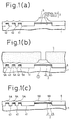
- a structure as shown in Fig. 1(a) is obtained by burying trenches 41 - 43 by a deposition means that conducts etching and deposition simultaneously (bias ECR-CVD process is used in this example). Then, an isotropic etching step for isotropically etching burying material 5 as shown by a broken line in Fig. 1(b) is applied before a polishing step to obtain a structure as shown in Fig. 1(c). Subsequently, a flat structure as shown in Fig. 1(d) is obtained by the polishing step.
- the burying material 5 on a wide protrusion region is etched by the isotropic etching step in Fig. 1(b) into a shape substantially uniform with other portions as shown in Fig. 1(c). Accordingly, a satisfactory flattening is attained by polishing remaining protruding portions.
- this example is put to the following steps (1) - (6).
- Example 2 each of the inventions in Claim 1, 3 is embodied to form trench isolation and manufacture a semiconductor device.
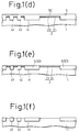
- the invention of claim 2 is applied particularly and it is embodied as a method of manufacturing a semiconductor device as defined in claim 4.
- Example 1 when the burying material is etched back as far as the upper portion of the trench opening in the state shown in Fig. 2(d), that is, when it is to be etched back by the thickness of the burying material on the protrusion region shown by 5C in Fig. 2(d), since the and point can not be judged, it is difficult to control the etching film thickness as the burying material 5 for the isolation portion shown in Fig. 2(e).
- Example 2 undertakes to overcome the problem.
- Example 2 since SiO2 which is the burying material after resist patterning can be etched as far as the surface of the stopper layer is exposed and the burying material (SiO2) on the protrusion region can be removed completely by polishing in the next step, etching back which is necessary in Example 1 is no more required.
- a substrate 1 to be formed with trench isolation has an etching stopper layer 2 comprising a three-layered structure as shown in Fig. 2(a), (b), (c), (d), trench isolation is formed in a structure in which the upper layer 23 (silicon nitride film in this example) of an etching stopper layer 2 is formed with a film having a polishing rate smaller than that of the burying material 5 and an etching rate also smaller than that of a burying material 5, an intermediate layer 22 (polysilicon film in this example) is formed with a film having an etching rate smaller than that of the upper layer 23, and a lower layer 21 (thermally oxidized silicon dioxide in this example) is formed with a film having an etching rate smaller than that of the intermediate layer 22 and an etching rate greater than that of the substrate.
- the upper layer 23 silicon nitride film in this example
- an etching stopper layer 2 is formed with a film having a polishing rate smaller than that of the burying material
- this example is put to the following steps (1) - (6).
- poly-Si as the intermediate layer 22 is removed, for example, with KOH, and T-SiO2 as the underlying layer 21 is removed by means of hydrofluoric acid.
- the poly-Si of the intermediate layer functions as a stopper to Si3N4 constituting the upper layer 23, while T-SiO2 constituting the lower layer 21 has a functions of an etching stopper to poly-Si of the intermediate layer 22.
- Examples 1 - 2 The examples are modified from Examples 1 - 2 described above. While isotropic etching is applied by wet etching using an etching solution before the polishing of the burying material in Examples 1, 2, isotropic etching was conducted by means of dry etching in these examples.
- the present invention is applied to a method of manufacturing a fine and integrated semiconductor device to be formed with trench isolation.
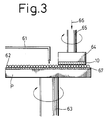
- Fig. 3 shows steps of this example.
- a plurality of protrusion patterns 61 - 63 were formed on a substrate 1 and trenches formed between each of the protrusions was buried.
- dummy patterns 71a - 71c and 72a - 72c constituting the polishing stopper layer were previously formed to provide a structure as shown in Fig. 3(a) in which protrusions were uniformly distributed, i.e., the ratio of the surface of the stopper layer 3 present was made uniform.
- a burying material 5 was deposited to obtain a structure as shown in Fig.
- flattened trench isolation was formed by the following steps (1) - (3).
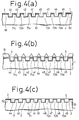
- the present invention was applied to the formation of trench isolation as shown in Fig. 4. While the bias ECR-CVD process was used in Example 1 for forming the burying oxide film, an atmospheric CVD process capable of forming an insulator film was used in this example. Description will be made in the order of steps.
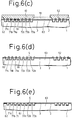
- the present invention was applied to the formation of trench isolation as shown in Fig. 6. Further, as a method of removing an excess burying material 5 (silicon oxide film), a silicon oxide film 51 present in a wide protrusion region was at least partially removed previously by etching using a resist process and, subsequently, a silicon oxide film 52 in a wide burying region including dummy patterns was removed by polishing. More specifically, it was practiced as shown below.
- silicon oxide film 51 present in a wide protrusion region was at least partially removed previously by etching using a resist process and, subsequently, a silicon oxide film 52 in a wide burying region including dummy patterns was removed by polishing. More specifically, it was practiced as shown below.
- the present invention was applied to the formation of a fine and integrated semiconductor device and, in particular, to the formation of trench isolation thereof.
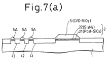
- a structure as shown in Fig. 7(a) was obtained by a burying step of burying a plurality of recesses 41 - 43 on a substrate 1 by a bias ECR-CVD process as a deposition means for simultaneously conducting etching and deposition. Then, a structure as shown in Fig. 7(c) was obtained by conducting a polishing step of flattening a burying material by polishing (Fig. 7(b)), a resist forming step of forming a resist on the substrate after the polishing step and a resist pattern forming step of exposing the burying material remaining in the portions other than the recesses to be buried (the burying material 52 not removed completely).
- a removing step of removing the burying material 52 remaining in the portions other than the recesses to be buried was conducted using a resist pattern 6 as a mask thereby attaining a satisfactory burying and flattening with no residue of the burying material not removed completely, as shown in Fig. 7(d).
- this example was put to the following steps (1) - (6).
- Example 9 the present invention was embodied to the formation of trench isolation for manufacturing a semiconductor device.
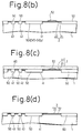
- the resist was patterned, the lithographic step therefor took much time but the patterning could be saved in this Example 9.
- This example was put to the following steps (1) - (4).
- Fig. 9(a) - (f) shows the steps in this example.
- a plurality of protrusion patterns 61 - 63 each having a polishing stopper layer 3 in the upper portion were formed as shown in Fig. 9(a) and recesses 41 - 47 defined by the plurality of protrusion patterns were buried by a burying material 5 as shown in Fig. 9(b).
- a second polishing stopper layer 7 was formed at least on the burying material 5 in the recess of the portion in which the density of the polishing stopper layer 3 was coarse (wide recess) 41 as shown in Fig. 9(c) and Fig. 9(d) (in this example, after forming the second polishing stopper layer 7 over the entire surface as in Fig.
- flattened trench isolation was formed by the following steps (1) - (6).
- the present invention was applied to trench isolation.
- atmospheric CVD and vacuum CVD were used for forming a burying oxide film and a polishing stopper layer.
- a bias ECR-CVD process (this method is suitable as burying and flattening technique since etching and deposition are conducted simultaneously) was applied to the formation of the buried and flattened film and the second polishing stopper layer, thereby forming a polishing stopper layer 7 over the entire surface of a recess 41 as a trench.
- the following steps (1) - (7) were conducted.
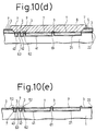
- a poly-Si layer 22 as an etching stopper layer for a Si3N4 layer as a stopper layer 3 for polishing and the Si3N4 layer as the polishing stopper layer 3 on a semiconductor substrate 1 such as made of silicon trenches were formed by a RIE (reactive ion etching) step using a resist process. Then, a structure as shown in Fig. 10(a) was obtained.
- RIE reactive ion etching
- the polishing stopper layer may take various modes such that the material, processing conditions, etc. can be appropriately varied so long as the polishing stopper layer has a polishing rate lower than that of the burying material layer.
- flattening can be attained without leaving the burying material on a wide (long) protrusion region, whereby it is possible to provide a means capable of forming trench isolation of satisfactory flatness, as well as a means for manufacturing a semiconductor device formed with such trench isolation.
- the present invention it is possible to provide a method of manufacturing a semiconductor device having a polishing step for conducting flattening after burying, wherein satisfactory flattened shape can be formed even in a portion in which the area ratio of a stopper layer per unit area is low in a case where there is unevenness in the distribution of a portion showing a function of a polishing stopper on the portion to be polished.
Abstract
Description
- The present invention concerns a method of forming trench isolation having a polishing step and a method of manufacturing a semiconductor device having a polishing step. The present invention can be applied to the formation of trench isolation (trench type inter-device separation) in various kinds of electronic materials, a method of manufacturing various kinds of semiconductor devices having trench isolation, as well as a method of manufacturing various kinds of semiconductor devices having a recess burying step and a subsequent flattening and polishing step. Further, it can be utilized as a method of manufacturing a semiconductor device having a polishing step including a step of burying recesses defined with a plurality of protrusion patterns (that is, defined between each of protrusion patterns) by a burying material and a step of flattening the burying material formed on the protrusion patterns by polishing.
- The polishing technique has a wide application use and it can be utilized, for example, for flattening unevenness resulting in a substrate such as a semiconductor substrate upon manufacturing a semiconductor device (refer, for example, to Japanese Patent Laid Open sho 63-39835).
- On the other hand, the capacitance of a device has been increased in the field of semiconductor devices and various kinds of techniques have been developed in order to increase the capacitance while minimizing a chip area as small as possible and, for example, a multi-layered wiring technique is indispensable therefor. In the multi-layered wiring technique, it is extremely important to flatten the underlying substrate in order to prevent disconnection of the multi-layred wiring. This is because unevenness on the underlying substrate, if any, will lead to occurrence of wire disconnection on a step caused by the unevenness (so-called step disconnection). In order to flatten the underlying substrate satisfactorily, flattening from the initial stage is important.
- For attaining the above-mentioned purpose, there has been considered, for example, a flat trench isolation. Trench isolation is a technique for inter-device isolation by burying an insulator to trenches formed on a semiconductor substrate and it is advantageous for higher degree integration since fine trenches can be formed. However, after burying the trenches, it is necessary to remove protrusions composed of a burying material deposited to the portions other than the trenches for attaining a flattened surface. The trench can be formed as a recess between two protrusion patterns but, when a burying material is buried in the recess (trench), since the burying material is also deposited on the protrusion patterns other than the trench to form a protruding portion, it has to be flattened. A method as shown in Fig. 11 has been known as a method of forming a flat trench isolation.
- In this method, as shown in Fig. 11 (A), a thin
silicon oxide film 2 and a thinsilicone nitride film 3 are formed on asemiconductor substrate 1, then trenches 41, 42 and 43 are formed by etching using a photolithographic step and, subsequently, an inner wall oxide film, that is, thesilicon oxide layer 2 is formed by oxidation to provide a semiconductor substrate. - Then, as shown in Fig. 11 (B), a
burying material 5 is deposited in the trenches 41-43 by a deposition means, for example, CVD to obtain a structure as shown in the figure. In this case, theburying material 5 is deposited to a large thickness also to the portions other than the trenches 42 - 43 to result inprotrusions 51. - Accordingly, as shown in Fig. 11 (C), the
protrusions 51 are removed to flatten by polishing. In a case where a silicone oxide is used as theburying material 5, asilicon nitride film 3 having a polishing speed lower than that may be used for instance as a stopper layer for polishing. - Such a method is applied, in addition to the trench isolation process, also to other processes for forming flat interlayer insulation films such as formation of a trench capacitor accompanying trench burying, formation of trench contact (trench plug) or formation of a layer by a blanket W-CVD process.
- However, in a case where a wide recessed region (1) and a narrow protruding region (2) are formed as shown in Fig. 12(A). When polishing is applied directly after burying the trenches 41 - 43, the burying material 52 (SiO₂ or the like) not removed completely remains in the central portion of the
burying material 5 on the wide protruding region (1), and SiO₂ or the like which is theburying material 52 is raised to result in occurrence of particles when the stopper layer 2 (for example) Si₃N₄ is removed by hot phosphoric acid in the succeeding step. - As a countermeasure for overcoming the problem, for instance, IBM has presented the following technique in IEDM in 1989 (IEDM 89, pp 61 - 64). That is, as shown in Fig. 13(a), a block resist 31 is formed in the recess of CVD-SiO₂ as the
burying material 5, on which aresist coating film 3 is formed which are then etched back. Thus, a structure as shown in Fig. 13(b) is obtained. Then, it is flattened by polishing to obtain a flattened structure as shown in Fig. 13(c). However, in this method, if a patterning for the block resist is displaced to form a resist out of the recess as shown by reference numeral 31' in Fig. 13(d), no sufficient flatness can be obtained even if a resist coating film 3' is formed, so that theburying material 5 does not become flat as shown in Fig. 13(e) and, as a result, it is difficult to flatten by means of polishing. - In addition, there is also the following problem. That is, the flattening technique by polishing involves a problem that the extent of polishing depends on the underlying pattern and sometimes it results in unevenness. Description will now be made to the problem with reference to Fig. 14.
- In Fig. 14, trenches 41 - 43 are formed as recesses between each of protrusion patterns 61 - 64. The protrusion patterns 61 - 64 function as a stopper upon polishing. As shown in Fig. 14, the density of the
protrusion pattern 61 is small or course in the portion A of the figure in which theprotrusion pattern 61 is present. In the portion B shown in the figure in which the protrusion patterns 62 - 64 are present, a ratio of the protrusion patterns in a unit area (the area ratio of the protrusion patterns) is great and, accordingly, the density of the protrusion pattern is large or dense. In the illustrated embodiment, since silicon nitride or the like as a polishing stopper layer is formed on the protrusion patterns 61 - 64, the area of thestopper layer 3 in the unit area is small and, accordingly, the density thereof is coarse in the illustrated portion A. On the other hand, since the area of thestopper layer 3 in the unit area is large, the density of thepolishing stopper 3 is dense in the illustrated portion B shown in the figure. If there is unevenness of the ratio of the polishing stopper layer 3 (which exists each for the protrusion patterns 61 - 64), polishing tends to become uneven. - For instance, in a peripheral circuit, if the area ratio per unit area of a protrusion pattern present there that function as a polishing stopper layer is low (for example, in a case of the region A in Fig. 14), since a polishing pressure is concentrated upon polishing to the protrusion pattern (stopper layer), the polishing rate is increased, so that mere selection ratio of the protrusion pattern (stopper layer) is insufficient and an
isolation pattern 61 is scraped off as shown in Fig. 14(b) which no more provides an intended effect as the stopper layer. As a result, the region A is concaved and uniform and satisfactory flattening can not be attained as shown in Fig. 14(b). - Accordingly, it has been demanded for a technique capable of attaining satisfactory flattening by polishing also in a case where the distribution of the polishing stopper layer shows unevenness (for instance, in a case where there is an unevenness for the density of protrusion patterns and, accordingly, there is an unevenness for the ratio of the polishing stopper layer) and also for a portion in which the area ratio is low, that is, a portion of a circuit pattern in which the portion that functions as the polishing stopper is coarse.
- It is an object of the present invention to overcome the foregoing problems in the prior art and provide a means capable of flattening without leaving a burying material on a wide (long) protrusion region thereby capable of forming trench isolation of satisfactory flatness, as well as a method of manufacturing a semiconductor device formed with such trench isolation.
- Another object of the present invention is to provide a method of manufacturing a semiconductor device having a polishing step of applying flattening after burying, wherein a satisfactory flattened shape can be formed even in a case where a distribution of a portion exhibiting the function of a polishing stopper on a portion to be polished has unevenness, also in a portion in which an area ratio of the stopper layer per unit area is low.
- The foregoing object can be attained by the present invention of
claim 1, concerning a method of forming trench isolation including a burying step of burying trenches by a deposition means for conducting etching and deposition simultaneously and a polishing step of flattening a burying material by polishing, wherein the method comprises at least an isotropic etching step for isotropically etching the burying material before the polishing step. - The foregoing object can be attained by the present invention of
claim 2, concerning a method of forming trench isolation as defined inclaim 1, wherein trenches are formed in a structure which has an etching stopper layer comprising a three-layered structure, and in which the upper layer of the etching stopper layer comprises a film having a polishing rate smaller than that of the burying material and an etching rate also smaller than that of the burying material, an intermediate layer of the etching stopper layer comprises a film having an etching rate smaller than that of the upper layer and a lower layer of the etching stopper layer comprises a film having an etching rate smaller than that of the intermediate layer and greater than that of the substrate. - The foregoing object can be attained by the present invention of
claim 3, concerning a method of manufacturing a semiconductor device of forming trench isolation by using the method of forming trench isolation as defined inclaim 1. - The foregoing object can be attained by the present invention of claim 4, concerning a method of manufacturing a semiconductor device of forming trench isolation by using the method of forming trench isolation as defined in
claim 2. - The foregoing object can be attained by the present invention of
claim 5, concerning a method of manufacturing a semiconductor device for forming trench isolation, which comprises a burying step of burying trenches by a bias ECR-CVD process, an isotropic etching step of isotropically etching a burying material thereby etching the burying material on a wide protrusion region and a polishing step of flattening the burying material by polishing. - The foregoing object can be attained by the present invention of
claim 6, concerning a method of manufacturing a semiconductor device for forming trench isolation by forming trenches in a structure, in which a substrate to form trench isolation has an etching stopper layer compri sing a three-layered structure, in which the upper layer of the etching stopper layer comprises silicon nitride, an intermediate layer of the etching stopper layer comprises polysilicon and a lower layer of the etching stopper layer comprises a silicon dioxide film. - The foregoing object can be attained by the present invention of
claim 7, concerning a method of manufacturing a semiconductor device having a polishing step including a step of burying recesses defined with a plurality of protrusion patterns by a burying material and a polishing step of flattening the burying material formed on the protrusion patterns by polishing, which comprises previously forming a pattern that constitutes a stopper layer for polishing and that is not intended directly for the function as a wiring or insulation portion, to a portion in which the density of the stopper layer for polishing is coarse. - The foregoing object can be attained by the present invention of
claim 8, concerning a method of manufacturing a semiconductor device having a polishing step as defined inclaim 7, wherein the patterns by polishing, which comprises previously forming a pattern that constitutes a stopper layer for polishing and that is not intended directly for the function as a wiring or insulation portion is finally removed. - The foregoing object can be attained by the present invention of claim 9, concerning a method of manufacturing a semiconductor device having a polishing step including a step of burying recesses defined with a plurality of protrusion patterns with a burying material on a semiconductor substrate having the plurality of protrusion patterns comprising a wide protrusion regions and narrow protrusion regions, and a step of flattening the burying material formed on the protrusion patterns by polishing, wherein the method comprises a step of previously forming a pattern that constitutes a stopper layer for polishing and that is finally removed to a portion in which the density of the stopper layer for polishing is coarse, and a step of at least partially etching the burying material on the wide protrusion regions prior to the flattening step by polishing.
- The foregoing object can be attained by the present invention of
claim 10, concerning a method of manufacturing a semiconductor device in which a plurality of protrusion patterns are formed on a substrate and trenches comprising recesses defined therebetween are buried, wherein a pattern as a stopper layer for polishing is previously formed to a portion in which the density of the protrusion patterns formed with the stopper layer for polishing is coarse to obtain a structure having the protrusions being uniformly distributed, thereby making the area ratio of the stopper layer uniform, subsequently, burying material is deposited and then the burying material on the protrusion patterns and the previously formed patterns are removed by polishing to obtain a flattened structure. - The foregoing object can be attained by the present invention of
claim 11, concerning a method of manufacturing a semiconductor device as defined in any one ofclaims 7 to 10, wherein the burying material is silicon dioxide and the layer as the polishing stopper comprises silicon nitride. - The foregoing object can be attained by the present invention of claim 12, concerning a method of manufacturing a semiconductor device as defined in any one of
claims 7 to 11, wherein the burying material is silicon dioxide and a bias ECR-CVD process is used for the formation of the burying material. - The foregoing object can be attained by the present invention of claim 13, concerning a method of manufacturing a semiconductor device as defined in any one of
claims 7 to 11, wherein the burying material is silicon dioxide and an atmospheric pressure CVD process is used for the formation of the burying material. - The foregoing object can be attained by the present invention of claim 14, concerning a method of manufacturing a semiconductor device as defined in claim 13, wherein CVD silicon dioxide is formed by using an organic silicon gas.
- The foregoing object can be attained by the present invention of claim 15, concerning a method of manufacturing a semiconductor device as defined in claim 9, wherein the layer constituting the polishing stopper comprises silicon nitride and a step of at least partially removing the burying material on the wide protrusion region prior to the flattening step by polishing utilizes a means of applying isotropic etching while masking other positions than the etched portion with a resist.
- The foregoing object can be attained by the present invention of claim 16, concerning a method of manufacturing a semiconductor device including a burying step for forming a recess burying material by a deposition means on a substrate formed with a plurality of recesses and a polishing step of flattening the burying material by polishing, wherein the method comprises a resist forming step of forming a resist on the substrate after the polishing step, a resist pattern forming step of forming a resist pattern while exposing the burying material remaining in the portions other than the recesses to be buried, and a removing step of removing the burying material remaining in the portions other than the recesses to be buried by using the resist pattern as a mask.
- The foregoing object can be attained by the present invention of claim 17, concerning a method of manufacturing a semiconductor device including a burying step for forming recess burying material by a deposition means on a substrate formed with a plurality of recesses and a polishing step of flattening the burying material by polishing, wherein the method comprises a flattened layer forming step of forming a flattened layer on the substrate, and an etching back step for etching back under the condition in which an etching rate is equal between the flattened layer and the burying material.
- The foregoing object can be attained by the present invention of claim 18, concerning a method of manufacturing a semiconductor device which comprises burying silicon dioxide as a burying material into a plurality of recesses on a substrate having a silicon nitride film as a stopper layer for polishing by a base CR-CVD process and then conducting a polishing step of flattening the burying material by polishing, conducting a resist forming step of forming a resist on a substrate after the polishing step and a resist pattern forming step of forming a resist pattern while exposing the burying material remaining in the portion other than recesses to be buried as the burying material not removed completely and, subsequently, conducting a removing step of removing the burying material remaining in the portion other than the recesses to be buried by using the resist pattern as a mask, thereby conducting burying and flattening with no residue of the burying material not removed completely.
- The foregoing object can be attained by the present invention of claim 19, concerning a method of manufacturing a semiconductor device which comprises a burying step of forming a recess burying material by depositing silicon dioxide by a bias ECR-CVD process on a substrate in which a plurality of recesses are formed and a silicon nitride film is formed as a stopper layer for polishing stopper, a polishing step of flattening the burying material by polishing, a flattened layer forming step of forming a flattened layer on a substrate by a resist or SOG and an etching back step of applying etching back in a condition in which an etching rate is made equal between the flattened layer and the burying material.
- The foregoing object can be attained by the present invention of claim 20, concerning a method of manufacturing a semiconductor device having a polishing step including a step of forming a plurality of protrusion patterns each having a stopper layer for polishing in the upper portion, a step of burying recesses defined with a plurality of protrusion patterns by a burying material and a step of flattening the burying material formed on the protrusion patterns by polishing, wherein the method comprises forming a second polishing stopper layer at least on the recess burying material after burying the recesses.
- The foregoing object can be attained by the present invention of
claim 21, concerning a method of manufacturing a semiconductor device including a step of forming a plurality of protrusion patterns each having a stopper layer for polishing in the upper portion, a step of burying a plurality of recesses comprising wide recesses and narrow recesses defined with a plurality of protrusion patterns by a burying material and a step of flattening the burying material formed on the protrusion patterns by polishing, wherein the method comprises forming a second stopper layer for polishing at least on the entire surface of the recess burying material after burying the recesses. - The foregoing object can be attained by the present invention of
claim 22, concerning a method of manufacturing a semiconductor device which comprises forming a plurality of protrusion patterns on a substrate having a silicon nitride layer as a stopper layer for polishing and a poly-Si layer as an etching stopper layer of the silicon nitride layer in the upper portion, forming silicon dioxide as a burying material in recesses defined with a plurality of protrusion patterns by a CVD process, burying the recesses, subsequently, forming a second stopper layer for polishing over the entire surface, leaving a second stopper layer for polishing only on the burying material in a wide recess in a portion in which the density of the stopper layer for polishing is coarse by an etching step using a resist, and, thereafter, flattening the burying material formed on the recesses by polishing. - The foregoing object can be attained by the present invention of
claim 23, concerning a method of manufacturing a semiconductor device as defined inclaim 22, wherein silicon dioxide as the burying material is formed by a O₃-TEOS CVD process. - The foregoing object can be attained by the present invention of claim 24, concerning a method of manufacturing a semiconductor device as defined in any one of claims 20 to 23, wherein the burying material and the stopper layer for polishing are formed by a CVD process.
- The foregoing object can be attained by the present invention of claim 25, concerning a method of manufacturing a semiconductor device as defined in any one of claims 20 to 23, wherein the burying material and the stopper layer for polishing are formed by a deposition means for applying etching and deposition simultaneously.
- The foregoing object can be attained by the present invention of claim 26, concerning a method of manufacturing a semiconductor device as defined in claim 25, wherein the deposition means for applying etching and deposition simultaneously is a bias ECR-CVD process.
- The foregoing object can be attained by the present invention of claim 27, concerning a method of manufacturing a semiconductor device as defined in claim 25 or 26, wherein the second stopper layer for polishing is formed over the entire surface of the recesses that constitute trenches.
- According to the present invention, most of the material to be polished on the wide (long) protrusion region is removed in the etching step prior to the polishing and, since all of the remaining portions to be polished are in a protruding shape, the polishing rate therefor is faster than that for the flattened surface to facilitate flattening. This enables flattened formation of isolation.
- For instance, the upper layer of the etching stopper layer functions as an etching stopper upon etching the burying material and, further, the
intermediate layer 22 functions as a stopper for the upper layer 23 (refer to Fig. 2) and the lower layer functions as an etching stopper to theintermediate layer 22 and, accordingly, etching for the burying material can be applied till the surface of the stopper layer is exposed and, further, the burying material remaining on the protrusion region can be removed completely without requiring etching back. - Further, according to the present invention, a semiconductor device having satisfactorily flattened trench isolation can be obtained.
- Further, according to the present invention, a pattern that functions as a stopper layer for polishing and that is not intended directly for a function as a wiring or insulation portion (which hereinafter sometimes referred to as a dummy pattern) is formed, for example, to a portion in which the density of a protrusion pattern functioning as a polishing stopper is coarse, previously before polishing, for example, before deposition of the burying material by CVD or the like, so that the function of the stopper layer can be made nearly uniform over the entire surface of the portion to be polished, the dummy pattern is preferably formed such that the area ratio of the stopper layer is greater than a predetermined ratio and then the polishing is applied. Accordingly, satisfactory flattened shape can be formed.
- Therefore, according to the present invention, it is possible to form a satisfactory flattened shape even in a case where the area ratio of the polishing stopper layer per unit area in the portion to be polished is low.
- Further, according to the present invention, the material to be polished on the wide (long) protrusion region, if it remains after polishing, can easily be removed by a removed step using a resist pattern as a mask to conduct flattening, by which it is possible to manufacture a semiconductor device in which flat burying is attained.
- Further, according to the present invention, the material to be polished on the wide (long) protrusion region, if it remains after polishing, can be easily removed by the etching back step to conduct flattening. This enables to manufacture a semiconductor device capable of attaining flat burying.
- Further, according to the present invention, after burying the recesses and depositing the burying material, for example, by CVD, the second polishing stopper layer is formed at least on the recess burying material, for example, on the recess burying material in a portion where the density of the polishing stopper layer is coarse, by which the stopper function can be made nearly uniform over the entire surface of the portion to be polished, the area ratio of the stopper layer can be increased preferably to greater than a predetermined ratio and, thereafter, polishing is applied. Consequently, a uniform and satisfactory flattened shape can be obtained.
- Therefore, according to the present invention, it is possible to form a satisfactory flattened shape even in a case where the area ratio of the polishing stopper layer per unit area of the polished portion is low.
- Further, according to the present invention, after burying the recesses, for example, after depositing the burying material by CVD or the like, a second polishing stopper layer is formed at least over the entire surface of the recess burying material, so that the stopper function can be made nearly uniform over the entire surface of the polished portion and the area ratio of the stopper can be increased, preferably, to greater than a predetermined ratio and, subsequently, polishing is applied. Accordingly, a uniform and satisfactory flattened shape can be obtained.
- Therefore, according to the present invention, a satisfactory flattened shape can be formed even in a case where the area ratio of the polishing stopper layer per unit area of the polished portion is low.
-
- Fig. 1(a) - (f) shows steps in Example 1;
- Fig. 2(a) - (e) shows steps in Example 2;
- Fig. 3 shows a polisher device used in each of examples;
- Fig. 4(a) - (c) shows steps in Example 5;
- Fig. 5(a) - (d) shows steps in Example 6;
- Fig. 6(a) - (e) shows steps in Example 7;
- Fig. 7(a) - (f) shows steps in Example 8;
- Fig. 8(a) - (e) shows steps in Example 9;
- Fig. 9(a) - (f) shows steps in Example 10;
- Fig. 10(a) - (g) shows steps in Example 11;
- Fig. 11(A) - (C) shows steps in the prior art;
- Fig. 12(A) - (B) shows problems in the prior art;
- Fig. 13(a) - (e) shows problems in the prior art; and
- Fig. 14(a) - (b) shows problems in the prior art.
- Descriptions will now be made to preferred embodiments according to the present invention with reference to the drawings.
- It will be apparent that the present invention is not restricted to the following example.
- In this example, each of inventions in
claims 1 to 3 of the present application are embodied. That is, the present invention is applied to the formation of fine and integrated a semiconductor device which is made and, more in particular, to the formation of trench isolation thereof. - In this example, a structure as shown in Fig. 1(a) is obtained by burying trenches 41 - 43 by a deposition means that conducts etching and deposition simultaneously (bias ECR-CVD process is used in this example). Then, an isotropic etching step for isotropically
etching burying material 5 as shown by a broken line in Fig. 1(b) is applied before a polishing step to obtain a structure as shown in Fig. 1(c). Subsequently, a flat structure as shown in Fig. 1(d) is obtained by the polishing step. - The burying
material 5 on a wide protrusion region is etched by the isotropic etching step in Fig. 1(b) into a shape substantially uniform with other portions as shown in Fig. 1(c). Accordingly, a satisfactory flattening is attained by polishing remaining protruding portions. - More specifically, this example is put to the following steps (1) - (6).
- (1) A
lower layer 21 which is a thermally oxidized film (T-SiO₂) and anupper layer 23 which is a poly Si film are formed to a substrate 1 (silicon substrate in this example) to constitute astopper layer 2. Further, trenches 41 - 43 are formed and a layer of the buryingmaterial 5 is formed to the Si trenches by forming a SiO₂ film to a thickness greater than the depth of the trench by an ECR-CVD process. Thus, a structure as shown in Fig. 1(a) is obtained. CVD conditions in this case may be set, for example, as: microwave = 1000 W, RF = 500 W, SiH₄/H₂O = 21/35 sccm, magnetic field = 875 gauss and pressure = 7 x 10⁻⁴ torr. - (2) As shown in Fig. 1(b), resist 3 is patterned so as to remain in other portions than a wide (long) protrusion region (1).
- (3) SiO₂ which is the burying
material 5 is isotropically etched by isotropic etching. For instance, this may be attained by wet etching using a solution of hydrofluoric acid diluted to 1/40. In this case, it is not necessary to completely remove SiO₂ above the upper layer 23 (poly-Si) but it may be left as it is. That is, it may suffice to etch as far as the same film thickness as that of narrow protrusions. The protruding shape of the portion is shown by B. Subsequently, the resist 3 is removed to obtain a structure shown in Fig. 1(c). - (4) Polishing is applied by using a polisher. A device as shown in Fig. 3 can be used as a polisher. The polishing conditions in this case may be set as: number of rotation of a polishing plate P = 37 rpm, number of rotation of wafer holder specimen table 64 = 17 rpm, polishing pressure (shown by
arrow 66 in Fig. 2) = 8 psi, slurry introduction rate from aslurry introduction pipe 61 = 225 ml/min and temperature of apad 67 = 40oC. As a slurry (shown schematically as 62 in Fig. 3), a mixture of silica, KOH and water can be used. For instance, as a polishing solution (slurry) used for polishing, SC-1 (name of products manufactured by Cabot Corporation) can be used. The solid ingredient is silica (30% based on the entire weight) (pH: 10.5 - 10.7, silica grain size: 25 - 35 nm, pH controller: KOH). SC-1 is diluted to 15 - 20 times with deionized water and it is used under pH control by a solution of diluted hydrochloric acid or KOH and NaOH. In Fig. 3 are shown arotational shaft 63 for the polishing plate P, arotational shaft 65 for the wafer holder specimen table 64 that supports a wafer as asubstrate 10 to be polished.
Upon polishing, only theprotrusion portions SiO₂ protrusion 5A as the buryingmaterial 5 over the narrow protrusion region can be formed only by the bias ECR-CVD capable of conducting sputter etching and CVD simultaneously but such protruding shape can not be formed by a conformal CVD. Accordingly, it may be polished in the shape as it is formed into a film. Thus, a structure as shown in Fig. 1(d) can be obtained. - (5) Then, SiO₂ as the burying
material 5 is etched back till the poly-Si surface as theupper layer 23 is exposed. It can be conducted, for instance, by using a magnetron RIE under the conditions as: C₄F₈ = 50 sccm, RF = 1200 W and pressure = 2 Pa. Thus, a structure as shown in Fig. 1(e) can be obtained. - (6) Subsequently, poly-Si of the
upper layer 23 and T-SiO₂ of thelower layer 21 formed as the etching stopper of poly-Si may be eliminated. - Descriptions will be made to Example 2. Also in this example, each of the inventions in
Claim claim 2 is applied particularly and it is embodied as a method of manufacturing a semiconductor device as defined in claim 4. - In Example 1, when the burying material is etched back as far as the upper portion of the trench opening in the state shown in Fig. 2(d), that is, when it is to be etched back by the thickness of the burying material on the protrusion region shown by 5C in Fig. 2(d), since the and point can not be judged, it is difficult to control the etching film thickness as the burying
material 5 for the isolation portion shown in Fig. 2(e). Example 2 undertakes to overcome the problem. - In Example 2, since SiO₂ which is the burying material after resist patterning can be etched as far as the surface of the stopper layer is exposed and the burying material (SiO₂) on the protrusion region can be removed completely by polishing in the next step, etching back which is necessary in Example 1 is no more required.
- In this example, a
substrate 1 to be formed with trench isolation has anetching stopper layer 2 comprising a three-layered structure as shown in Fig. 2(a), (b), (c), (d), trench isolation is formed in a structure in which the upper layer 23 (silicon nitride film in this example) of anetching stopper layer 2 is formed with a film having a polishing rate smaller than that of the buryingmaterial 5 and an etching rate also smaller than that of a buryingmaterial 5, an intermediate layer 22 (polysilicon film in this example) is formed with a film having an etching rate smaller than that of theupper layer 23, and a lower layer 21 (thermally oxidized silicon dioxide in this example) is formed with a film having an etching rate smaller than that of theintermediate layer 22 and an etching rate greater than that of the substrate. - More specifically, this example is put to the following steps (1) - (6).
- (1) A structure to be formed with trench isolation is formed so as to have an etching stopper layer of a three-layered structure, in which the
uppermost layer 23 is made, for example, of Si₃N₄ as the material for the polishing stopper layer for SiO₂ as the buryingmaterial 5, theintermediate layer 22 is made, for example, of polysilicon as the material of an etching stopper to the upper layer 23 (Si₃N₄) and thelower layer 21 is made for example, of SiO₂ as the material having the etching rate smaller than that of theintermediate layer 22 and an etching rate greater than that of Si as the material for theunderlying substrate 1, trenches 41 - 43 formed in this structure are buried to just the same depth as that of the trench by a bias ECR-CVD method as a deposition means capable of conducting etching and deposition simultaneously. The CVD conditions may be identical with those in Example 1. This can provide a structure as shown in Fig. 2(a). In the drawing, are shown a buryingmaterial 5A buried in awide trench 41, buryingmaterials material 5 over a wide protrusion region (1) and buryingmaterials - (2) Resist 3 is patterned to portions other than the wide (long) protrusion area (1). Thus, a structure as shown in Fig. 2(b) can be obtained.
- (3) Isotropic etching is applied to etch the burying
material 5d on the wide (long) protrusion region (1). For instance, wet etching may be applied, for example, by using a solution prepared by diluting, for example, hydrofluoric acid to 1/40 concentration. The ratio of the etching rate between the CVD-SiO₂ as the buryingmaterial 5d and Si₂₃N₄ as theupper layer 23 to hydrofluoric acid is about 8:1 if over etching is conducted as far as the Si₃N₄ surface of theupper layer 23 is exposed, there is no problem at all. Subsequently, the resist is removed. Thus, a structure as shown in Fig. 4(c) is obtained. - (4)
Portions 50 of protruding shape formed by isotropic etching in the step (3) above are eliminated by polishing. In this case, since flattening can be attained by flattening only theprotrusion portions 50, the polishing time can be shortened.
Further, since the ratio of the polishing rate between SiO₂ as the buryingmaterial 5 and Si₃N₄ as the material for theupper layer 23 is about 5:1, Si₃N₄ functions sufficienlty as the stopper layer. Thus, a structure as shown in Fig. 2(d) is formed. - (5) Then, SiO₂ as the burying
material 5 is etched back till the Si₃n₄ surface as theupper layer 23 is exposed. This can be attained by using, for example, magnetron RIE and under the conditions as C₄F₈ = 50 sccm, RF = 1200 W, pressure = 2 Pa. Thus, a structure as shown in Fig. 2(d) can be obtained. - (6) Then, the
etching stopper layer 2 is removed. At first, Si₃N₄ as theupper layer 23 is removed by using, for example, magnetron RIE and under the conditions as: C₄F₈ = 50 sccm, RF = 1200 W, pressure = 2 Pa. Further, Si₃N₄ may be removed by using hot phosphoric acid. - Next, poly-Si as the
intermediate layer 22 is removed, for example, with KOH, and T-SiO₂ as theunderlying layer 21 is removed by means of hydrofluoric acid. - In this case, the poly-Si of the intermediate layer functions as a stopper to Si₃N₄ constituting the
upper layer 23, while T-SiO₂ constituting thelower layer 21 has a functions of an etching stopper to poly-Si of theintermediate layer 22. - The examples are modified from Examples 1 - 2 described above. While isotropic etching is applied by wet etching using an etching solution before the polishing of the burying material in Examples 1, 2, isotropic etching was conducted by means of dry etching in these examples.
- In the examples, SiO₂ as the burying
material 5 was isotropically dry etched under the following conditions, instead of etching by hydrofluoric acid in Examples 1 and 2: Etching apparatus used: parallel flat type ether
Pressure: 2300 mtorr (306 Pa)
RF power: 550 W
Gas system used: NF₃ = 300 cc/min
He = 200 cc/min
Temperature: 80oC
Satisfactory isotropic etching could be attained by the conditions described above. The conditions was set in order to increase the power for conducting reaction using fluoric acid radicals as a main etchant and increase the pressure for reducing the directionality of ions (to shorten the mean free path), thereby attaining isotropic etching. - Other procedures were the same as those in Examples 1 and 2. Also in these examples, satisfactory trench isolation was formed and highly reliable semiconductor devices could be obtained in the same manner as in Examples 1 and 2.
- In this example, the present invention is applied to a method of manufacturing a fine and integrated semiconductor device to be formed with trench isolation. Fig. 3 shows steps of this example.
- In this example, a plurality of protrusion patterns 61 - 63 were formed on a
substrate 1 and trenches formed between each of the protrusions was buried. For a portion in which the density of the protrusion patterns 61 - 63 to which the polishingstopper layer 3 was formed (illustrated portion) was thin,dummy patterns 71a - 71c and 72a - 72c constituting the polishing stopper layer were previously formed to provide a structure as shown in Fig. 3(a) in which protrusions were uniformly distributed, i.e., the ratio of the surface of thestopper layer 3 present was made uniform. Subsequently, a buryingmaterial 5 was deposited to obtain a structure as shown in Fig. 6(b) and then the buryingmaterial 51 on the protrusion patterns 61 - 63 and, particularly, formedpatterns 71a - 71c, 72a - 72c (hereinafter referred to sometimes also as "dummy pattern") were removed by polishing to obtain a flattened structure as shown in Fig. 3(c). - Specifically, in this example, flattened trench isolation was formed by the following steps (1) - (3).
- (1) As shown in Fig. 3(a), after forming a thermally oxidized film as a
silicon oxide layer 2 and a Si₃N₄ layer as a polishingstopper layer 3 on asemiconductor substrate 1 such as made of silicon, protrusion patterns 61 - 63 actually used as circuit patterns, etc. anddummy patterns 71a - 71c, 72a - 72c were formed simultaneously by an etching step using a resist process so that the area ratio of thestopper layer 3 per unit area is greater than a predetermined ratio irrespective of the positions on the semiconductor wafer.
As the etching conditions in this example, the following conditions were used for instance.
Gas system used: C₂Cl₃F₃/SF₈ = 60/10 (sccm)
Microwave power: 850 (W)
RF power: 150 (W)
Pressure: 1.33 (Pa) - (2) Then, the trenches 41 - 48 were buried by a CVD process. Thus, a structure as shown in Fig. 3(b) was obtained. In this example, burying was conducted by depositing a silicon oxide film by a bias ECR-CVD process having a high burying performance and capable of providing a satisfactory buried flattened shape (since etching and deposition were conducted simultaneously in this method, it was satisfactory as the burying flattening technique). As the bias ECR-CVD conditions, the following conditions were used for instance.
Gas system used: SiN₄/N₂O = 20/35 (sccm)
Microwave power: 1000 (W)
RF power: 500 (W)
Magnetic flux density: 8.75 x 10⁻² (T)
Pressure: 9.3 x 10⁻² (Pa) - (3) Then, excess burying material 51 (SiO₂) on the protrusion patterns 61 - 63 and the
dummy patterns 71a - 71c, 72a - 72c was removed by a polishing process. Thus, a structure as shown in Fig. 3(c) was obtained. As a polishing device in this example, a customary device shown in Fig. 3 was used. The polishing was conducted under the conditions, for example, as shown below.
Number of rotation of a polishing plate: 37 (rpm)
Number of rotation of a wafer holder specimen table: 17 (rpm)
Polishing pressure: 5.5 x 10³ (Pa)
Slurry flow rate: 225 (ml/min)
Pad temperature: 40 (oC)
Slurry: silica (0.025 - 0.035 um)
KOH (pH ≦ 10.5) - In the polishing step, the selection ratio between the stopper layer (Si₃N₄) and the burying material 5 (SiO₂) was at SiO₂/Si₃N₄ = 4/6, and the area ratio of the stopper layer per unit area was increased by the provision of the
dummy patterns 71a - 71c, 72a - 72c even in the periphery of theisolation pattern 61 in which the distribution of the protrusion patterns was thin, so that excess polishing for theisolation pattern 61 caused by overpolishing could be prevented, to attain a satisfactory flattened surface. - In this example, the present invention was applied to the formation of trench isolation as shown in Fig. 4. While the bias ECR-CVD process was used in Example 1 for forming the burying oxide film, an atmospheric CVD process capable of forming an insulator film was used in this example. Description will be made in the order of steps.
- (1) In a
silicon substrate 1 in which poly-Si as anetching stopper layer 8 and asilicon oxide layer 2 as an etching stopper layer for the stopper layer 8 (poly-Si) therebelow were formed, for instance, protrusion patterns 61 - 63 includingactual patterns 61, as well aspatterns 71a - 71c and 72a - 72c to be removed subsequently were formed simultaneously by an etching process using a resist process such that the area ratio of the stopper layer per unit area was formed greater than a predetermined ratio irrespective of positions on the wafer, in a portion corresponding to awide recess trench 41 explained in Fig. 14 in the same manner as in Example 5. In this case, a microwave etching device was used and the process was carried out, for example, under the following conditions.
Gas system used: C₂Cl₃F₃/SF₆ = 60/10 (sccm)
Microwave power: 850 (W)
RF power: 150 (W)
Pressure: 1.33 (Pa)
Then, silicon oxide was formed through reaction, for example, between an organic silicon compound (for example, TEOS) and ozone as a buryingmaterial 5, which was buried to about such a film thickness as burying the trenches. Thus, a structure as shown in Fig. 4(a) was obtained. The process was conducted under the CVD conditions, for example, as shown below.
Gas system used: TEOS/O₃ = 350/350 (sccm)
Growing temperature: 390 (oC)
Pressure: 1.20 x 10⁴ (Pa)
However, since a recessed amount (L₁) was present for the shape of the silicon oxide layer after it was buried in this step as shown in Fig. 4(a), the thickness of the remaining film in the trench recess after polishing was made smaller than the depth of the trench, failing to obtain a satisfactory flattened shape. - (2) Then, in this example, a coating film 9 was coated to such a film thickness as capable of absorbing the recessed amount (L₁) in the silicon oxide film as shown in Fig. 4(b). For instance, SOG (Spin On Glass) may be used for the formation of the coating film 9 for instance. The film thickness may be adjusted to 1/2 - 1 times as great as the trench depth. As the SOG coating conditions, the following conditions were employed, for instance.
Coating film:Type 7 manufactured by Tokyo Ohka Co.
Number of rotation: 4000 (rpm)
Time: 60 (sec)
Baking temperature: 400 (oC)
Baking time: 30 (min) - (3) Then, as shown in Fig. 4(c), polishing was applied till the SOG film 9 on the trench protrusions was removed as shown in Fig. 4(b), i.e., by the film thickness L₂ of the SOG film 9. In this case, since the SOG film 9 had a greater polishing rate than that of the silicon oxide film as the burying
material 5, the silicon oxide film functions as a stopper layer for the SOG film 9. - (4) Then, etching back was applied till the upper surface of the
etching stopper layer 8 was exposed under the conditions that the etching selection ratio between the silicon oxide film as the buryingmaterial 5 and the SOG film 9 is at 1. Thus, a flattened structure as shown in Fig. 4(d) was obtained. As the conditions using RIE in this case, the following condition can be selected for instance.
Gas system use: CHF₃/O₂ = 70/13 (sccm)
RF power: 1150 (W)
Pressure: 5.33 (Pa) - In this example, the present invention was applied to the formation of trench isolation as shown in Fig. 6. Further, as a method of removing an excess burying material 5 (silicon oxide film), a
silicon oxide film 51 present in a wide protrusion region was at least partially removed previously by etching using a resist process and, subsequently, asilicon oxide film 52 in a wide burying region including dummy patterns was removed by polishing. More specifically, it was practiced as shown below. - (1) As shown in Fig. 6(a), after forming a thermally oxidized film as a
silicon oxide layer 2 and a Si₃n₄ layer as a polishingstopper layer 3 on asemiconductor substrate 1 such as made of silicon, protrusion patterns 61 - 63 including thepattern 61 actually used as a circuit pattern, anddummy patterns 71a - 71c and 72a - 72c were formed simultaneously by an etching step using a resist process such that the area ratio of thestopper layer 3 per unit area is greater than a predetermined ratio, irrespective of positions on the wafer. In this case, as the conditions when a microwave etching device was used, the following conditions were employed for instance.
Gas system used: C₂Cl₃F₃/SF₆ = 60/10 (sccm)
Microwave power: 850 (W)
RF power: 150 (W)
Pressure: 1.33 (Pa) - (2) Then, the trenches were buried by a CVD process. In this example, trenches were buried by using the silicon oxide film using a bias ECR-CVD process having a high burying performance and providing satisfactory burying flattened shape. As the bias ECR-CVD conditions in this case, the following conditions were employed for instance.
Gas system used: SiH₄/N₂O = 20/35 (sccm)
Microwave power: 1000 (W)
RF power: 500 (W)
Magnetic flux density: 8.75 x 10⁻² (T)
Pressure: 9.3 x 10⁻² (Pa)
Thus, a structure as shown in Fig. 6(b) was obtained.Reference numeral 51 denotes a burying material on the wide protrusion region, while 52 denotes a burying material on the narrow protrusion region. - (3) Then, as shown in Fig. 6(c), resist 10 was formed by patterning to portions other than the wide (long) protrusion region.
- (4) The
silicon oxide film 51 as an excess buryingmaterial 5 on the wide (long) protrusion region was removed by isotropic etching. As the etching conditions in this case, the following conditions were used for instance. Liquid etching by HF : H₂O = 1:40
The selection ratio between SiO₂ and Si₃N₄ in this case was about 8:1.
Further, the excesssilicon oxide film 51 on the wide (long) protrusion region could be etched with no trouble at all till theunderlying Si₃N₄ layer 3 was exposed. Subsequently, the resist 10 was removed. Thus, a structure as shown in Fig. 6(d) was obtained. - (5) The excess protruding
silicon oxide film 52 formed in the step (4) above was removed by polishing. Since only the excess protrudingsilicon oxide 52 was flattened by polishing in this case, the polishing time could be shortened and, since the polishing selection ratio of Si₃N₄ to SiO₂ was 5:1, Si₃N₄ could serve sufficiently as the stopper layer, a satisfactory flattened shape as shown in Fig. 6(e) could be obtained. - In this example, the present invention was applied to the formation of a fine and integrated semiconductor device and, in particular, to the formation of trench isolation thereof.
- In this example, a structure as shown in Fig. 7(a) was obtained by a burying step of burying a plurality of recesses 41 - 43 on a
substrate 1 by a bias ECR-CVD process as a deposition means for simultaneously conducting etching and deposition. Then, a structure as shown in Fig. 7(c) was obtained by conducting a polishing step of flattening a burying material by polishing (Fig. 7(b)), a resist forming step of forming a resist on the substrate after the polishing step and a resist pattern forming step of exposing the burying material remaining in the portions other than the recesses to be buried (the buryingmaterial 52 not removed completely). Subsequently, a removing step of removing the buryingmaterial 52 remaining in the portions other than the recesses to be buried was conducted using a resistpattern 6 as a mask thereby attaining a satisfactory burying and flattening with no residue of the burying material not removed completely, as shown in Fig. 7(d). - More specifically, this example was put to the following steps (1) - (6).
- (1) A
lower layer 21 as a SiO₂ pad made of a thermally oxidized film (T-SiO₂) and anupper layer 22 made of a silicon nitride (Si₃N₄) film were formed to a substrate 1 (silicon substrate in this example) to constitute astopper layer 2. Further, recesses 41 - 43 as trenches were formed and a SiO₂ film was formed in the Si trenches to the same thickness as the depth of the trenches by means of a bias ECR-CVD process to form a layer of a buryingmaterial 5. Thus, a structure as shown in Fig. 7(a) was obtained. As the CVD conditions in this case, the following conditions can be used for instance.
Microwave = 1000 W
RF = 500 W
SiH₄/N₂O = 21/35 sccm
Magnetic field = 8.75 x 10⁻⁴ T
Pressure = 9.3 x 10⁻² Pa (7 x 10⁻⁴ Torr) - (2) Then, polishing was by a polisher, as the polisher, the device as shown in Fig. 3 can be used. Polishing was conducted under conditions: number of rotation of a polishing plate P = 37 rpm, number of rotation of a wafer holder specimen table 64 = 17 rpm, polishing pressure (shown by
arrow 66 in Fig. 2) = 5.5 x 10³ Pa (8 psi), slurry introduction rate from aslurry introduction pipe 61 = 225 ml/min and temperature of apad 67 = 40oC. As a slurry (shown schematically by 62 in Fig. 3), a mixture of silica, KOH and water can be used. For instance, as a polishing solution (slurry) used for polishing, SC-1 (name of products manufactured by Cabot Corporation) can be used. The solid ingredient is silica (30% based on the entire weight) (pH: 10.5 - 10.7, silica grain size: 25 - 35 um, pH controller: KOH). SC-1 is diluted to 15 - 20 times with deionized water and it can be used under pH control by a solution of diluted hydrofluoric acid or KOH and NaOH. In Fig. 3, are shown arotational shaft 63 for the polishing plate P, arotational shaft 65 for the wafer holder specimen table 64 that supports a wafer as asubstrate 10 to be polished.
In this case, the shape of theSiO₂ protrusion 5A as the buryingmaterial 5 on the narrow protrusion region (Fig. 7) in the surface to be polished can be formed only by the bias ECR-CVD capable of conducting sputter etching and CVD simultaneously but such protruding shape can not be formed by conformal CVD. Since such protruding shape of SiO₂ can be polished easily SiO₂ 52' which can not be removed completely but remains on the narrow protrusion region (line and space pattern) as the prior art (Fig. 12(b)), does not occur in the case of using the bias ECR-CVD. A structure as shown in Fig. 7(b) was obtained by the polishing step.Reference numeral 50 denotes the material buried in the recesses 41 - 43. - (3) A resist was patterned in the portions other than the central portion on a long protrusion to obtain a structure having a resist
pattern 6 as shown in Fig. 7(c). Since the patterning is not fine patterning, a sufficient margin is available for aligning accuracy. - (4) Remaining (not removed completely) SiO₂ not masked with the resist
pattern 6 was etched to obtain a structure as shown in Fig. 7(d). It may be removed by wet etching using HF, or it may be removed by etching using RIE, for example, magnetron RIE under the following conditions.
C₄F₈ = 50 sccm
RF = 1200 W
Pressure = 2 Pa - (5) Then, the resist was removed. The resist may be removed by using a RA stripper or using an ECR asher under the following conditions. Thus, a structure as shown in Fig. 7(e) was obtained.
O₂/CHF₃ = 400/20 sccm
Pressure = 1.9 Pa (1.4 Torr)
Microwave = 400 mA
Substrate temperature = 150oC - (6) Then, Si₃N₄ as the
upper layer 22 of thestopper layer 2 was removed, for example, with KOH and the pad-SiO₂ as thelower layer 21 was removed with hydrofluoric acid to obtain a structure as shown in Fig. 7(f). - Description will now be made to Example 9. In this example, the present invention was embodied to the formation of trench isolation for manufacturing a semiconductor device. In Example 1, since the resist was patterned, the lithographic step therefor took much time but the patterning could be saved in this Example 9. This example was put to the following steps (1) - (4).
- (1) In the same manner as in Example 8, a structure as shown in Fig. 8(a) was obtained by forming a SiO₂ film as a burying
material 5 by means of bias ECR-CVD process in Si trenches to the same thickness as the depth of trenches in which a pad SiO₂ as alower layer 21 and Si₃N₄ as anupper layer 22 were formed. The CVD conditions in this example may be the same as those in Example 8. - (2) Polishing was applied by using a polisher to obtain a structure as shown in Fig. 8(b). The polishing conditions in this case may be the same as those in Example 8.
- (3) A resist was coated to obtain a structure as shown in Fig. 8(c). For instance, the resist was coated under the following conditions.
Resist = OFPR-800, manufactured by Tokyo Ohka Co.
Viscosity = 0.02 Pa.s
Number of rotation = 8000 rpm
Further, SOG (spin on glass) may also be used instead of the resist and the process can be practiced under the following conditions.
SOG = type-2, manufactured by Tokyo Ohka Co.
Number of rotation = 200 rpm
Rotational time = 15 s
Baking temperature = 500oC
Baking time = 300 min. - (4) Etching back was applied at a ratio of resist : SiO₂ = 1 : 1, to etch back the resist 6 and the remaining
SiO₂ 52. Thus, a structure as shown in Fig. 8(d) was obtained. The etching could be applied by using, for example, a parallel flat plate RIE device under the following conditions.
CHF₃ = 50 sccm
O₂ = 70 sccm
RF power = 1200 W
Pressure = 30 Pa
Etching back at a ratio of SOG : SiO₂ = 1 : 1 can be conducted under the same conditions.
Since there was less residual SiO₂, SiO₂ could be removed sufficient even by such an etching back process. - (5) Then, Si₃N₄ as the
upper layer 22 of astopper layer 2 was removed, for example, with KOH and a pad SiO₂ as thelower layer 21 was removed with hydrofluoric acid to obtain a structure as shown in Fig. 16(e). - In this example, the present invention was applied to a method of manufacturing a fine and integrated semiconductor device formed with trench isolation. Fig. 9(a) - (f) shows the steps in this example.
- In this example, a plurality of protrusion patterns 61 - 63 each having a polishing
stopper layer 3 in the upper portion were formed as shown in Fig. 9(a) and recesses 41 - 47 defined by the plurality of protrusion patterns were buried by a buryingmaterial 5 as shown in Fig. 9(b). After burying the recesses, a secondpolishing stopper layer 7 was formed at least on the buryingmaterial 5 in the recess of the portion in which the density of the polishingstopper layer 3 was coarse (wide recess) 41 as shown in Fig. 9(c) and Fig. 9(d) (in this example, after forming the secondpolishing stopper layer 7 over the entire surface as in Fig. 9(c) and, subsequently, the secondpolishing stopper layer 7 was left only on the buryingmaterial 5 in thewide recess 41 by an etching step using a resist 8 as shown in Fig. 9(d)). Then, a step of flattening the burying material formed on the protrusion pattern with polishing was conducted. - As a result, since the second
polishing stopper layer 7 was formed on the buryingmaterial 5 in thewide recess 41 also to the portion in which the density of the polishingstopper layer 3 was coarse from the initial stage, no excess polishing proceeds even near theisolation protrusion pattern 61 and uniform and satisfactory flattening could be attained by polishing. - Specifically, in this example, flattened trench isolation was formed by the following steps (1) - (6).
- (1) As shown in Fig. 9(a), after forming a thermally oxidized film as a
silicon oxide layer 21, a poly-Si layer as anetching stopper layer 22 for a Si₃N₄ layer which is a polishingstopper layer 3 and the Si₃N₄ layer as the polishingstopper layer 3 on asemiconductor substrate 1 such as made of silicon, recesses 41 - 43 as trenches were formed by a RIE (reactive ion etching) step using a resist process. As the RIE conditions in this case, the following conditions were employed for instance.
Gas system used: C₂Cl₃F₃/SF₆ = 60/10 (sccm)
Microwave power: 850 (W)
RF power: 150 (W)
Pressure: 1.33 (Pa) - (2) Then, as shown in Fig. 9(b), a burying
material 5 for burying the recesses 41 - 43 as the trenches was formed, for example, from an organic silicon compound (for example, TEOS) and ozone (O₃) by a CVD process such that the film thickness in therecess 41 of the trench was smaller than the depth of the trench by the thickness of the polishing stopper layer (a in the figure). As the TEOS/O₃ CVD conditions, the following conditions were employed for instance.
Gas system employed: TEOS/O₃ = 1000/2000 (sccm)
Growing temperature: 390 (oC)
Pressure: 1.20 x 10⁴ (Pa) - (3) Successively, as shown in Fig. 9(c), a silicon nitride film as a second polishing stopper layer was formed. The thickness of the silicon nitride film in this case was set such that the thickness of the silicon oxide film and the thickness of the silicon nitride film in the trench recess 41 (a+b in the figure) was made equal with the trench depth. As the conditions for forming the silicon nitride film, the following conditions were employed for instance.
Gas system used: SiH₂Cl₂/NH₃ = 50/200 (sccm)
Growing temperature: 760 (oC)
Pressure: 70 (Pa).
In this case, as shown in Fig. 9(c), a resistpattern 8 was formed in order to remove the secondpolishing stopper layer 7 formed in the portions other than thewide recess 41 of the trench. - (4) Then, an excess silicon nitride film was etched by isotropic etching. Thus, as shown in Fig. 9(d), the second
polishing stopper layer 7 was left only on the buryingmaterial 5 in thewide recess 41. The etching was conducted in this case under the following etching conditions, for instance.
Etching solution used: phosphoric acid
Temperature: 150 (oC) (The selection ratio between the silicon nitride film and the silicon oxide film was about 50:1) - (5) SiO₂ as the excess burying
material 5 formed on the protrusion of the trench and the silicon nitride film as the secondpolishing stopper layer 7 left in the form of a protrusion on the trench recess 41 (indicated by a protrusion 31) were removed and flattened by polishing. Thus, a structure as shown in Fig. 9(e) was obtained. In this case, a customary device as shown in Fig. 3 was used as the polishing device. The polishing was conducted in this case under the following polishing conditions for instance.
Number of rotation of polishing plate: 37 (rpm)
Number of rotation of wafer holder specimen table: 17 (rpm)
Polishing pressure: 5.5 x 10³ (Pa)
Slurry flow rate: 225 (ml/min)
Pad temperature: 40 (oC)
Slurry: Silica (0.025 - 0.03 um)
KOH (pH ≦ 10.5)
Water
In the polishing step, since the selection ratio between the polishingstopper layers 3, 7 (Si₃N₄) and the burying material 5 (SiO₂) was at SiO₂/Si₃N₄ = 4 - 6, and the area ratio of Si₃N₄ as the stopper material per unit area was greater than a predetermined ratio irrespective of positions on the wafer, a sufficiently flattened shape could be obtained with no over polishing for theisolation pattern 61.
Further, in flattening by the polishing method, it has been generally known that protrusion has much greater polishing rate than that of a flattened portion made of an identical material and, for instance, if aprotrusion 31 shown in Fig. 7(d) should occur, satisfactory flattened shape could be obtained. - (6) Then, etching back was conducted entirely by magnetron RIE using poly-Si of the
etching stopper layer 22 as a stopper. As the etching conditions in this case, the following conditions were employed, for instance.
Gas system used: C₃F₈/O₂ = 45/15 (sccm)
RF power: 1200 (W)
Pressure: 2 (Pa)
Finally, poly-Si as theetching stopper layer 22 and SiO₂ as thesilicon oxide layer 21 were removed with KOH and hydrofluoric acid respectively. Thus, trench isolation as shown in Fig. 9(f) was completed. - In this example, the present invention was applied to trench isolation. In Example 10, atmospheric CVD and vacuum CVD were used for forming a burying oxide film and a polishing stopper layer. In this example, a bias ECR-CVD process (this method is suitable as burying and flattening technique since etching and deposition are conducted simultaneously) was applied to the formation of the buried and flattened film and the second polishing stopper layer, thereby forming a polishing
stopper layer 7 over the entire surface of arecess 41 as a trench. The following steps (1) - (7) were conducted. - In the same manner as in Example 10, after forming a thermally oxidized
film 21 as a silicon oxide layer, a poly-Si layer 22 as an etching stopper layer for a Si₃N₄ layer as astopper layer 3 for polishing and the Si₃N₄ layer as the polishingstopper layer 3 on asemiconductor substrate 1 such as made of silicon trenches were formed by a RIE (reactive ion etching) step using a resist process. Then, a structure as shown in Fig. 10(a) was obtained. As the RIE conditions in this case, the following conditions were employed, for instance.
Gas system used: C₂Cl₃F₃/SF₆ = 60/10 (sccm)
Microwave power: 850 (W)
RF power: 150 (W)
Pressure: 1.33 (Pa) - (2) Then, a silicon oxide film was buried as a burying
material 5 in trench recesses 41 - 43 by a bias ECR-CVD process having a high burying performance and providing a satisfactory buried and flattened shape. The buried film was formed such that the film thickness in the trench recesses 41 - 43 was less than the trench depth by the thickness of the polishingstopper layer 3 as shown in Fig. 10(b). As the bias ECR-CVD conditions in this case, the following conditions were employed, for instance.
Gas system used: SiH₄/N₂O = 20/35 (sccm)
Microwave power: 1000 (W)
RF power: 500 (W)
Magnetic flux density: 8.75 x 10⁻² (T)
Pressure: 9.3 x 10⁻² (Pa) - (3) Successively, a silicon nitride film as the polishing
stopper layer 3 was formed by a bias ECR-CVD process. The silicon nitride film was formed to such a thickness as at least greater than the thickness of the polishingstopper layer 3 upon forming the trenches. Thus, a structure as shown in Fig. 10(c) was obtained. As the bias ECR-CVD conditions in this case, the following conditions were employed, for instance.
Gas system used: SiH₄/N₂/Ar = 20/20/15 (sccm)
Microwave power: 550 (W)
RF power: 200 (W)
Magnetic flux density: 8.75 x 10⁻² (T)
Pressure: 2.0 x 10⁻¹ (Pa)
Since the bias ECR-CVD process utilizes a simultaneous competing reaction between deposition and etching (sputter etching), it has dependency an angle of plane. Accordingly, the film was not formed in the regions other than those having a certain angle of plane relative to the horizontal plane of the substrate and provided a shape of the film as shown in Fig. 10(c). - (4) As shown in Fig. 10(d). a resist 8 was formed by patterning on the portions other than the long trench protrusion (protrusions on the right and left in the figure) as shown in Fig. 10(d).
- (5) At first, silicon nitride films on the right and left in the figure as the second
polishing stopper layer 7 formed on the protrusions of the long trenches were removed by isotropic etching using the resist 8. As etching conditions in this case, the following conditions were used for instance.
Etching solution used: Phosphoric acid
Temperature: 150 (°C) (selection ratio between the silicon nitride film and the silicon oxide film was about 50:1)
Then, successively, the silicon oxide film as the excess buryingmaterial 5 on the long protrusion was removed by isotropic etching. As the etching conditions in this case, the following conditions were employed for instance.
Etching solution used: HF:H₂O = 1:40
Temperature: 150 (°C) (selection ratio between the SiO₂ film and the Si₃N₄ film was about 8:1)
In this case, the excess silicon oxide film on the long protrusion was underlying polishingstopper layers - (6) The excess
silicon oxide film 52 in the form of protrusions formed in the preceding step (S) were removed by polishing. Since only the excess protrudingsilicon oxide film 52 was flattened, the polishing time could be shortened. Further, since the area ratio of the polishingstopper layers 3, 7 (Si₃N₄) per unit area was greater than a predetermined ratio, irrespective of positions on the wafer, it was possible to obtain a sufficiently flattened shape without overpolishing the isolation pattern 61 (refer to Fig. 14(e)). Thus, a structure as shown in Fig. 10(f) could be obtained. - (7) Then, etching back was applied for the entire surface by magnetron RIE under the conditions of SiO₂ and Si₃N₄ selection ration at 1:1. As the etching back conditions in this case, the following conditions were employed, for instance.
Gas system used: C₃F₈ = 45/15 (sccm)
RF power: 1200 (W)
Pressure: 2 (Pa) - It will be apparent that the present invention is not restricted only to the examples but each of the constitutions may be selected properly unless it goes beyond the scope of the invention. For instance, the polishing stopper layer may take various modes such that the material, processing conditions, etc. can be appropriately varied so long as the polishing stopper layer has a polishing rate lower than that of the burying material layer.
- According to the present invention, flattening can be attained without leaving the burying material on a wide (long) protrusion region, whereby it is possible to provide a means capable of forming trench isolation of satisfactory flatness, as well as a means for manufacturing a semiconductor device formed with such trench isolation.
- Further, according to the present invention, it is possible to provide a method of manufacturing a semiconductor device having a polishing step for conducting flattening after burying, wherein satisfactory flattened shape can be formed even in a portion in which the area ratio of a stopper layer per unit area is low in a case where there is unevenness in the distribution of a portion showing a function of a polishing stopper on the portion to be polished.
Water
In Fig. 3, are shown a polishing plate P, a slurry introduction pipe 81, a slurry 82, a rotational shaft 83 for the polishing plate, a wafer holder specimen table 84, a rotational shaft 85 for the wafer holder specimen table, a pressure 86 adjusted upon polishing, a polishing pad 87 and a
Claims (27)
- A method of forming trench isolation including a burying step of burying trenches by a deposition means for conducting etching and deposition simultaneously and a polishing step of flattening a burying material by polishing, wherein
the method comprises at least an isotropic etching step for isotropically etching the burying material before the polishing step. - A method of forming trench isolation as defined in claim 1, wherein trenches are formed in a structure which has
an etching stopper layer comprising a three-layered structure, and in which
the upper layer of said etching stopper layer comprises a film having a polishing rate smaller than that of the burying material and an etching rate also smaller than that of the burying material,
an intermediate layer of said etching stopper layer comprises a film having an etching rate smaller than that of the upper layer and
a lower layer of said etching stopper layer comprises a film having an etching rate smaller than that of the intermediate layer and greater than that of the substrate. - A method of manufacturing a semiconductor device of forming trench isolation by using the method of forming trench isolation as defined in claim 1.
- A method of manufacturing a semiconductor device of forming trench isolation by using the method of forming trench isolation as defined in claim 2.
- A method of manufacturing a semiconductor device for forming trench isolation, which comprises
a burying step of burying trenches by a bias ECR-CVD process,
an isotropic etching step of isotropically etching a burying material thereby etching the burying material on a wide protrusion region and
a polishing step of flattening the burying material by polishing. - A method of manufacturing a semiconductor device for forming trench isolation by forming trenches in a structure, in which
a substrate to form trench isolation has an etching stopper layer comprising a three-layered structure, in which
the upper layer of said etching stopper layer comprises silicon nitride, an intermediate layer of said etching stopper layer comprises polysilicon and a lower layer of said etching stopper layer comprises a silicon dioxide film. - A method of manufacturing a semiconductor device having a polishing step including a step of burying recesses defined with a plurality of protrusion patterns by a burying material and a polishing step of flattening the burying material formed on the protrusion patterns by polishing, which comprises previously forming a pattern that constitutes a stopper layer for polishing and that is not intended directly for the function as a wiring or insulation portion, to a portion in which the density of the stopper layer for polishing is coarse.
- A method of manufacturing a semiconductor device having a polishing step as defined in claim 7. wherein the patterns by polishing, which comprises previously forming a pattern that constitutes a stopper layer for polishing and that is not intended directly for the function as a wiring or insulation portion is finally removed.
- A method of manufacturing a semiconductor device having a polishing step including a step of burying recesses defined with a plurality of protrusion patterns with a burying material on a semiconductor substrate having said plurality of protrusion patterns comprising a wide protrusion regions and narrow protrusion regions, and a step of flattening the burying material formed on the protrusion patterns by polishing, wherein the method comprises
a step of previously forming a pattern that constitutes a stopper layer for polishing and that is finally removed to a portion in which the density of the stopper layer for polishing is coarse, and
a step of at least partially etching the burying material on the wide protrusion regions prior to the flattening step by polishing. - A method of manufacturing a semiconductor device in which a plurality of protrusion patterns are formed on a substrate and trenches comprising recesses defined there-between are buried, wherein a pattern as a stopper layer for polishing is previously formed to a portion in which the density of the protrusion patterns formed with the stopper layer for polishing is coarse to obtain a structure having the protrusions being uniformly distributed, thereby making the area ratio of the stopper layer uniform, subsequently, a burying material is deposited and then the burying material on the protrusion patterns and said previously formed patterns are removed by polishing to obtain a flattened structure.
- A method of manufacturing a semiconductor device as defined in any one of claims 7 to 10, wherein the burying material is silicon dioxide and the layer as the polishing stopper comprises silicon nitride.
- A method of manufacturing a semiconductor device as defined in any one of claims 7 to 11, wherein the burying material is silicon dioxide and a bias ECR-CVD process is used for the formation of the burying material.
- A method of manufacturing a semiconductor device as defined in any one of claims 7 to 11, wherein the burying material is silicon dioxide and an atmospheric pressure CVD process is used for the formation of the burying material.
- A method of manufacturing a semiconductor device as defined in claim 13, wherein CVD silicon dioxide is formed by using an organic silicon gas.
- A method of manufacturing a semiconductor device as defined in claim 9, wherein the layer constituting the polishing stopper comprises silicon nitride and a step of at least partially removing the burying material on the wide protrusion region prior to the flattening step by polishing utilizes a means of applying isotropic etching while masking other positions than the etched portion with a resist.
- A method of manufacturing a semiconductor device including a burying step for forming a recess burying material by a deposition means on a substrate formed with a plurality of recesses and a polishing step of flattening the burying material by polishing, wherein the method comprises
a resist forming step of forming a resist on the substrate after the polishing step,
a resist pattern forming step of forming a resist pattern while exposing the burying material remaining in the portions other than the recesses to be buried, and
a removing step of removing the burying material remaining in the portions other than the recesses to be buried by using the resist pattern as a mask. - A method of manufacturing a semiconductor device including a burying step for forming recess burying material by a deposition means on a substrate formed with a plurality of recesses and a polishing step of flattening the burying material by polishing, wherein the method comprises
a flattened layer forming step of forming a flattened layer on the substrate, and
an etching back step for etching back under the condition in which an etching rate is equal between the flattened layer and the burying material. - A method of manufacturing a semiconductor device which comprises burying silicon dioxide as a burying material into a plurality of recesses on a substrate having a silicon nitride film as a stopper layer for polishing by a base CR-CVD process and then conducting a polishing step of flattening the burying material by polishing, conducting a resist forming step of forming a resist on a substrate after the polishing step and a resist pattern forming step of forming a resist pattern while exposing the burying material remaining in the portion other than recesses to be buried as the burying material not removed completely and, subsequently, conducting a removing step of removing the burying material remaining in the portion other than the recesses to be buried by using the resist pattern as a mask, thereby conducting burying and flattening with no residue of the burying material not removed completely.
- A method of manufacturing a semiconductor device which comprises:
a burying step of forming a recess burying material by depositing silicon dioxide by a bias ECR-CVD process on a substrate in which a plurality of recesses are formed and a silicon nitride film is formed as a stopper layer for polishing stopper,
a polishing step of flattening the burying material by polishing,
a flattened layer forming step of forming a flattened layer on a substrate by a resist or SOG and
an etching back step of applying etching back in a condition in which an etching rate is made equal between the flattened layer and the burying material. - A method of manufacturing a semiconductor device having a polishing step including a step of forming a plurality of protrusion patterns each having a stopper layer for polishing in the upper portion, a step of burying recesses defined with a plurality of protrusion patterns by a burying material and a step of flattening the burying material formed on the protrusion patterns by polishing, wherein
the method comprises forming a second polishing stopper layer at least on the recess burying material after burying the recesses. - A method of manufacturing a semiconductor device including a step of forming a plurality of protrusion patterns each having a stopper layer for polishing in the upper portion, a step of burying a plurality of recesses comprising wide recesses and narrow recesses defined with a plurality of protrusion patterns by a burying material and a step of flattening the burying material formed on the protrusion patterns by polishing, wherein the method comprises
forming a second stopper layer for polishing at least on the entire surface of the recess burying material after burying the recesses. - A method of manufacturing a semiconductor device which comprises forming a plurality of protrusion patterns on a substrate having a silicon nitride layer as a stopper layer for polishing and a poly-Si layer as an etching stopper layer of the silicon nitride layer in the upper portion, forming silicon dioxide as a burying material in recesses defined with a plurality of protrusion patterns by a CVD process, burying the recesses, subsequently, forming a second stopper layer for polishing over the entire surface, leaving a second stopper layer for polishing only on the burying material in a wide recess in a portion in which the density of the stopper layer for polishing is coarse by an etching step using a resist, and, thereafter, flattening the burying material formed on the recesses by polishing.
- A method of manufacturing a semiconductor device as defined in claim 22, wherein silicon dioxide as the burying material is formed by a O₃-TEOS CVD process.
- A method of manufacturing a semiconductor device as defined in any one of claims 20 to 23, wherein the burying material and the stopper layer for polishing are formed by a CVD process.
- A method of manufacturing a semiconductor device as defined in any one of claims 20 to 23, wherein the burying material and the stopper layer for polishing are formed by a deposition means for applying etching and deposition simultaneously.
- A method of manufacturing a semiconductor device as defined in claim 25, wherein the deposition means for applying etching and deposition simultaneously is a bias ECR-CVD process.
- A method of manufacturing a semiconductor device as defined in claim 25 or 26, wherein the second stopper layer for polishing is formed over the entire surface of the recesses that constitute trenches.
Applications Claiming Priority (15)
| Application Number | Priority Date | Filing Date | Title |
|---|---|---|---|
| JP34026091 | 1991-11-29 | ||
| JP340260/91 | 1991-11-29 | ||
| JP34026991 | 1991-11-29 | ||
| JP340269/91 | 1991-11-29 | ||
| JP34026091 | 1991-11-29 | ||
| JP34026991 | 1991-11-29 | ||
| JP36053091 | 1991-12-30 | ||
| JP360530/91 | 1991-12-30 | ||
| JP36053091 | 1991-12-30 | ||
| JP3567692 | 1992-01-27 | ||
| JP35676/92 | 1992-01-27 | ||
| JP3567692 | 1992-01-27 | ||
| JP28505292 | 1992-05-30 | ||
| JP285052/92 | 1992-05-30 | ||
| JP4285052A JP2874486B2 (en) | 1991-11-29 | 1992-09-30 | Method for forming trench isolation with polishing step and method for manufacturing semiconductor device |
Publications (3)
| Publication Number | Publication Date |
|---|---|
| EP0545263A2 true EP0545263A2 (en) | 1993-06-09 |
| EP0545263A3 EP0545263A3 (en) | 1996-01-10 |
| EP0545263B1 EP0545263B1 (en) | 2002-06-19 |
Family
ID=27521717
Family Applications (1)
| Application Number | Title | Priority Date | Filing Date |
|---|---|---|---|
| EP92120116A Expired - Lifetime EP0545263B1 (en) | 1991-11-29 | 1992-11-25 | Method of forming trench isolation having polishing step and method of manufacturing semiconductor device |
Country Status (3)
| Country | Link |
|---|---|
| US (1) | US5498565A (en) |
| EP (1) | EP0545263B1 (en) |
| DE (1) | DE69232648T2 (en) |
Cited By (18)
| Publication number | Priority date | Publication date | Assignee | Title |
|---|---|---|---|---|
| EP0664559A2 (en) * | 1994-01-17 | 1995-07-26 | Sony Corporation | Process for planarizing surface of a semiconductor device |
| WO1996027206A2 (en) * | 1995-02-24 | 1996-09-06 | Intel Corporation | Polysilicon polish for patterning improvement |
| GB2306050A (en) * | 1995-10-05 | 1997-04-23 | Nec Corp | Planarizing filled trench isolation semiconductor devices |
| US5629242A (en) * | 1994-01-07 | 1997-05-13 | Sony Corporation | Process for planarizing surface of a semiconductor device |
| EP0791227A1 (en) * | 1994-11-10 | 1997-08-27 | Intel Corporation | Forming a planar surface over a substrate by modifying the topography of the substrate |
| WO1998003992A1 (en) * | 1996-07-23 | 1998-01-29 | Siemens Aktiengesellschaft | Method of filling trenches in a substrate |
| WO1998007189A1 (en) * | 1996-08-13 | 1998-02-19 | Advanced Micro Devices, Inc. | Semiconductor trench isolation structure having improved upper surface planarity |
| EP0825644A1 (en) * | 1996-08-21 | 1998-02-25 | Motorola, Inc. | Integrated circuit having a dummy structure and method of making the same |
| EP0825645A1 (en) * | 1996-08-08 | 1998-02-25 | Siemens Aktiengesellschaft | Gapfill and planarization process for shallow trench isolation |
| US5792707A (en) * | 1997-01-27 | 1998-08-11 | Chartered Semiconductor Manufacturing Ltd. | Global planarization method for inter level dielectric layers of integrated circuits |
| EP0905756A2 (en) * | 1997-09-30 | 1999-03-31 | Siemens Aktiengesellschaft | Planarization of a non-conformal device layer in semiconductor fabrication |
| WO1999016124A2 (en) * | 1997-09-22 | 1999-04-01 | Siemens Aktiengesellschaft | Method for producing insulations grooves in a substrate |
| EP0926715A2 (en) * | 1997-12-23 | 1999-06-30 | Texas Instruments Incorporated | Chemical mechanical polishing for isolation dielectric planarization |
| US5949125A (en) * | 1995-04-06 | 1999-09-07 | Motorola, Inc. | Semiconductor device having field isolation with a mesa or mesas |
| US6107187A (en) * | 1999-06-17 | 2000-08-22 | Motorola, Inc. | Method for forming a semiconductor device |
| WO2002021581A2 (en) * | 2000-09-05 | 2002-03-14 | Motorola, Inc. | Method for uniform polish microelectronic device |
| EP1271631A1 (en) * | 2001-06-29 | 2003-01-02 | Interuniversitair Micro-Elektronica Centrum Vzw | A method for producing semiconductor devices using chemical mechanical polishing |
| US6555476B1 (en) | 1997-12-23 | 2003-04-29 | Texas Instruments Incorporated | Silicon carbide as a stop layer in chemical mechanical polishing for isolation dielectric |
Families Citing this family (60)
| Publication number | Priority date | Publication date | Assignee | Title |
|---|---|---|---|---|
| JP3060714B2 (en) * | 1992-04-15 | 2000-07-10 | 日本電気株式会社 | Manufacturing method of semiconductor integrated circuit |
| KR0151051B1 (en) * | 1995-05-30 | 1998-12-01 | 김광호 | Method of forming insulation film for semiconductor device |
| US5763325A (en) * | 1995-07-04 | 1998-06-09 | Fujitsu Limited | Fabrication process of a semiconductor device using a slurry containing manganese oxide |
| DE69623651T2 (en) * | 1995-12-27 | 2003-04-24 | Lam Res Corp | METHOD FOR FILLING TRENCHES ON A SEMICONDUCTOR DISC |
| US5863828A (en) * | 1996-09-25 | 1999-01-26 | National Semiconductor Corporation | Trench planarization technique |
| US5923991A (en) * | 1996-11-05 | 1999-07-13 | International Business Machines Corporation | Methods to prevent divot formation in shallow trench isolation areas |
| KR100226736B1 (en) * | 1996-11-07 | 1999-10-15 | 구본준 | Method of forming a device isolation film of semiconductor device |
| US5721172A (en) * | 1996-12-02 | 1998-02-24 | Taiwan Semiconductor Manufacturing Company, Ltd. | Self-aligned polish stop layer hard masking method for forming planarized aperture fill layers |
| US6025270A (en) * | 1997-02-03 | 2000-02-15 | Taiwan Semiconductor Manufacturing Company, Ltd. | Planarization process using tailored etchback and CMP |
| US6171896B1 (en) * | 1997-02-03 | 2001-01-09 | Taiwan Semiconductor Manufacturing Company | Method of forming shallow trench isolation by HDPCVD oxide |
| US5721173A (en) * | 1997-02-25 | 1998-02-24 | Kabushiki Kaisha Toshiba | Method of forming a shallow trench isolation structure |
| KR100230815B1 (en) * | 1997-03-18 | 1999-11-15 | 김영환 | Method of trench isolation for semiconductor device |
| JP3638778B2 (en) * | 1997-03-31 | 2005-04-13 | 株式会社ルネサステクノロジ | Semiconductor integrated circuit device and manufacturing method thereof |
| US5786262A (en) * | 1997-04-09 | 1998-07-28 | Taiwan Semiconductor Manufacturing Co., Ltd. | Self-planarized gapfilling for shallow trench isolation |
| US5728621A (en) * | 1997-04-28 | 1998-03-17 | Chartered Semiconductor Manufacturing Pte Ltd | Method for shallow trench isolation |
| US5731241A (en) * | 1997-05-15 | 1998-03-24 | Taiwan Semiconductor Manufacturing Company, Ltd. | Self-aligned sacrificial oxide for shallow trench isolation |
| US5811345A (en) * | 1997-09-18 | 1998-09-22 | Taiwan Semiconductor Manufacturing Co., Ltd. | Planarization of shallow- trench- isolation without chemical mechanical polishing |
| US6309947B1 (en) * | 1997-10-06 | 2001-10-30 | Advanced Micro Devices, Inc. | Method of manufacturing a semiconductor device with improved isolation region to active region topography |
| KR100239453B1 (en) * | 1997-11-06 | 2000-01-15 | 김영환 | Method of forming a device isolation film of semiconductor device |
| KR100237222B1 (en) * | 1997-11-24 | 2000-01-15 | 김규현 | Method for separating semiconductor device |
| US6395619B2 (en) * | 1997-12-05 | 2002-05-28 | Sharp Kabushiki Kaisha | Process for fabricating a semiconductor device |
| US5923993A (en) * | 1997-12-17 | 1999-07-13 | Advanced Micro Devices | Method for fabricating dishing free shallow isolation trenches |
| JPH11214499A (en) * | 1998-01-27 | 1999-08-06 | Mitsubishi Electric Corp | Fabrication of semiconductor device |
| JPH11220017A (en) * | 1998-01-30 | 1999-08-10 | Mitsubishi Electric Corp | Semiconductor device and its manufacture |
| JPH11233609A (en) * | 1998-02-13 | 1999-08-27 | Mitsubishi Electric Corp | Semiconductor device and its manufacturing method |
| US6093656A (en) * | 1998-02-26 | 2000-07-25 | Vlsi Technology, Inc. | Method of minimizing dishing during chemical mechanical polishing of semiconductor metals for making a semiconductor device |
| US7001713B2 (en) * | 1998-04-18 | 2006-02-21 | United Microelectronics, Corp. | Method of forming partial reverse active mask |
| US6004863A (en) * | 1998-05-06 | 1999-12-21 | Taiwan Semiconductor Manufacturing Company | Non-polishing sacrificial layer etchback planarizing method for forming a planarized aperture fill layer |
| US5880006A (en) * | 1998-05-22 | 1999-03-09 | Vlsi Technology, Inc. | Method for fabrication of a semiconductor device |
| TW396510B (en) | 1998-06-03 | 2000-07-01 | United Microelectronics Corp | Shallow trench isolation formed by chemical mechanical polishing |
| US6790742B2 (en) * | 1998-06-03 | 2004-09-14 | United Microelectronics Corporation | Chemical mechanical polishing in forming semiconductor device |
| JPH11354629A (en) * | 1998-06-10 | 1999-12-24 | Mitsubishi Electric Corp | Manufacture of semiconductor device and the semiconductor device |
| US6180525B1 (en) * | 1998-08-19 | 2001-01-30 | Micron Technology, Inc. | Method of minimizing repetitive chemical-mechanical polishing scratch marks and of processing a semiconductor wafer outer surface |
| US6365523B1 (en) * | 1998-10-22 | 2002-04-02 | Taiwan Semiconductor Maufacturing Company | Integrated high density plasma chemical vapor deposition (HDP-CVD) method and chemical mechanical polish (CMP) planarizing method for forming patterned planarized aperture fill layers |
| US7045435B1 (en) * | 1998-11-03 | 2006-05-16 | Mosel Vitelic Inc | Shallow trench isolation method for a semiconductor wafer |
| US6461932B1 (en) * | 1998-12-14 | 2002-10-08 | National Semiconductor Corporation | Semiconductor trench isolation process that utilizes smoothening layer |
| JP2000190207A (en) * | 1998-12-28 | 2000-07-11 | Tdk Corp | Polishing method, and manufacture of thin film magnetic head |
| US6869858B2 (en) * | 1999-01-25 | 2005-03-22 | Taiwan Semiconductor Manufacturing Company, Ltd. | Shallow trench isolation planarized by wet etchback and chemical mechanical polishing |
| KR100343136B1 (en) * | 1999-03-18 | 2002-07-05 | 윤종용 | Method for Chemical Mechanical Polishing using a double polishing stopper |
| US6197660B1 (en) * | 1999-04-29 | 2001-03-06 | Taiwan Semiconductor Manufacturing Company | Integration of CMP and wet or dry etching for STI |
| JP3566885B2 (en) * | 1999-06-02 | 2004-09-15 | シャープ株式会社 | Method for forming trench isolation and method for manufacturing semiconductor device |
| US7253047B2 (en) * | 1999-09-01 | 2007-08-07 | Micron Technology, Inc. | Semiconductor processing methods of forming transistors, semiconductor processing methods of forming dynamic random access memory circuitry, and related integrated circuitry |
| US6197677B1 (en) * | 1999-11-01 | 2001-03-06 | United Microelectronics Corp. | Method of depositing a silicon oxide layer on a semiconductor wafer |
| US6197691B1 (en) * | 1999-11-15 | 2001-03-06 | Chartered Semiconductor Manufacturing Ltd. | Shallow trench isolation process |
| JP4307664B2 (en) | 1999-12-03 | 2009-08-05 | 株式会社ルネサステクノロジ | Semiconductor device |
| JP3506645B2 (en) * | 1999-12-13 | 2004-03-15 | Necエレクトロニクス株式会社 | Semiconductor device and manufacturing method thereof |
| JP2003530713A (en) * | 2000-04-11 | 2003-10-14 | キャボット マイクロエレクトロニクス コーポレイション | Priority removal system for silicon oxide |
| US6423612B1 (en) | 2000-06-26 | 2002-07-23 | Advanced Micro Devices, Inc. | Method of fabricating a shallow trench isolation structure with reduced topography |
| US6403484B1 (en) | 2001-03-12 | 2002-06-11 | Chartered Semiconductor Manufacturing Ltd. | Method to achieve STI planarization |
| US6734080B1 (en) * | 2002-05-31 | 2004-05-11 | Advanced Micro Devices, Inc. | Semiconductor isolation material deposition system and method |
| US6916713B2 (en) * | 2002-11-05 | 2005-07-12 | Macronix International Co., Ltd. | Code implantation process |
| US7427361B2 (en) * | 2003-10-10 | 2008-09-23 | Dupont Air Products Nanomaterials Llc | Particulate or particle-bound chelating agents |
| US20050126588A1 (en) * | 2003-11-04 | 2005-06-16 | Carter Melvin K. | Chemical mechanical polishing slurries and cleaners containing salicylic acid as a corrosion inhibitor |
| US7419911B2 (en) * | 2003-11-10 | 2008-09-02 | Ekc Technology, Inc. | Compositions and methods for rapidly removing overfilled substrates |
| TW201222778A (en) * | 2010-11-18 | 2012-06-01 | Ind Tech Res Inst | Trench capacitor structures and method of manufacturing the same |
| CN103854965B (en) * | 2012-11-30 | 2017-03-01 | 中国科学院微电子研究所 | Planarization process method |
| US9859494B1 (en) | 2016-06-29 | 2018-01-02 | International Business Machines Corporation | Nanoparticle with plural functionalities, and method of forming the nanoparticle |
| US10134603B2 (en) * | 2016-09-22 | 2018-11-20 | Infineon Technologies Ag | Method of planarising a surface |
| US10074721B2 (en) | 2016-09-22 | 2018-09-11 | Infineon Technologies Ag | Method of fabricating a semiconductor wafer that includes producing a planarised surface having both a mesa surface and an insulating layer surface |
| US10636673B2 (en) | 2017-09-28 | 2020-04-28 | Taiwan Semiconductor Manufacturing Co., Ltd. | Method for forming semiconductor device structure |
Citations (6)
| Publication number | Priority date | Publication date | Assignee | Title |
|---|---|---|---|---|
| WO1986002777A1 (en) * | 1984-11-01 | 1986-05-09 | Ncr Corporation | Process for forming isolation regions in a semiconductor substrate |
| DE3625742A1 (en) * | 1985-08-05 | 1987-05-27 | Rca Corp | Integrated CMOS circuit and method of producing the circuit |
| EP0341898A2 (en) * | 1988-05-12 | 1989-11-15 | Advanced Micro Devices, Inc. | Improved method of planarization of topologies in integrated circuit structures |
| EP0407047A2 (en) * | 1989-07-03 | 1991-01-09 | Advanced Micro Devices, Inc. | Improved method of planarization of topologies in integrated circuit structures |
| EP0424905A2 (en) * | 1989-10-25 | 1991-05-02 | Sony Corporation | Semiconductor device manufacturing process |
| EP0424608A1 (en) * | 1989-10-25 | 1991-05-02 | International Business Machines Corporation | Forming wide dielectric filled isolation trenches in semiconductors |
Family Cites Families (6)
| Publication number | Priority date | Publication date | Assignee | Title |
|---|---|---|---|---|
| JPS59163817A (en) * | 1983-03-08 | 1984-09-14 | Nec Corp | Substrate for semiconductor device |
| JPS6484634A (en) * | 1987-09-28 | 1989-03-29 | Fujitsu Ltd | Manufacture of semiconductor device |
| JP2517751B2 (en) * | 1988-12-13 | 1996-07-24 | 松下電器産業株式会社 | Method for manufacturing semiconductor device |
| JPH02294050A (en) * | 1989-05-09 | 1990-12-05 | Sony Corp | Trench burying method |
| JP3231754B2 (en) * | 1989-10-25 | 2001-11-26 | ソニー株式会社 | Method for manufacturing semiconductor device |
| JP3123061B2 (en) * | 1990-06-13 | 2001-01-09 | ソニー株式会社 | Buried flattening method by bias ECR-CVD method |
-
1992
- 1992-11-25 US US07/981,831 patent/US5498565A/en not_active Expired - Lifetime
- 1992-11-25 EP EP92120116A patent/EP0545263B1/en not_active Expired - Lifetime
- 1992-11-25 DE DE69232648T patent/DE69232648T2/en not_active Expired - Fee Related
Patent Citations (6)
| Publication number | Priority date | Publication date | Assignee | Title |
|---|---|---|---|---|
| WO1986002777A1 (en) * | 1984-11-01 | 1986-05-09 | Ncr Corporation | Process for forming isolation regions in a semiconductor substrate |
| DE3625742A1 (en) * | 1985-08-05 | 1987-05-27 | Rca Corp | Integrated CMOS circuit and method of producing the circuit |
| EP0341898A2 (en) * | 1988-05-12 | 1989-11-15 | Advanced Micro Devices, Inc. | Improved method of planarization of topologies in integrated circuit structures |
| EP0407047A2 (en) * | 1989-07-03 | 1991-01-09 | Advanced Micro Devices, Inc. | Improved method of planarization of topologies in integrated circuit structures |
| EP0424905A2 (en) * | 1989-10-25 | 1991-05-02 | Sony Corporation | Semiconductor device manufacturing process |
| EP0424608A1 (en) * | 1989-10-25 | 1991-05-02 | International Business Machines Corporation | Forming wide dielectric filled isolation trenches in semiconductors |
Non-Patent Citations (5)
| Title |
|---|
| 1991 SYMPOSIUM ON VLSI TECHNOLOGY-DIGEST OF TECHNICAL PAPETRS MAY 28-30, 1991, 1991, NEW-YORK, pages 87-88, T. GOCHO ET AL. 'TRENCH ISOLATION TECHNOLOGY FOR 0.35 MICROMETER DEVICE BY BIAS ECR CVD' * |
| IBM TDB , vol. 21, no. 7, December 1978 NEW-YORK, pages 2734-2737, H.B. POGGE 'single mask self-aligned trench isolation/diffusion process' * |
| IBM TECHNICAL DISCLOSURE BULLETIN, vol. 27, no. 8, January 1985 NEW YORK US, pages 4700-4701, K.D. BEYER ET AL. 'GLASS PLANARIZATION BY STOP-LAYER POLISHING' * |
| IBM TECHNICAL DISCLOSURE BULLETIN, vol. 32, no. 9A, February 1990 NEW YORK US, pages 439-440, 'METHOD FOR PLANARIZING OVER SHALLOW TRENCHES FILLED WITH SILICON DIOXIDE.' * |
| IEDM 3-6 DEC. 1989, WASHINGTON, 1989 NEW-YORK, pages 61-64, B. DAVARI ET AL. 'A NEW PLANARIZATION TECHNIQUE, USING A COMBINATION OF RIE AND CHEMICAL MECHANICAL POLISH (CMP). ' * |
Cited By (37)
| Publication number | Priority date | Publication date | Assignee | Title |
|---|---|---|---|---|
| US5629242A (en) * | 1994-01-07 | 1997-05-13 | Sony Corporation | Process for planarizing surface of a semiconductor device |
| EP0664559A2 (en) * | 1994-01-17 | 1995-07-26 | Sony Corporation | Process for planarizing surface of a semiconductor device |
| EP0664559A3 (en) * | 1994-01-17 | 1995-11-22 | Sony Corp | Process for planarizing surface of a semiconductor device. |
| KR100371252B1 (en) * | 1994-01-17 | 2003-04-07 | 소니 가부시끼 가이샤 | Film Flattening Method in Semiconductor Devices |
| US6048800A (en) * | 1994-01-17 | 2000-04-11 | Sony Corporation | Process for planarizing surface of a semiconductor device |
| EP0977248A1 (en) * | 1994-01-17 | 2000-02-02 | Sony Corporation | Process for planarizing surface of a semiconductor device |
| EP0791227A1 (en) * | 1994-11-10 | 1997-08-27 | Intel Corporation | Forming a planar surface over a substrate by modifying the topography of the substrate |
| EP0791227A4 (en) * | 1994-11-10 | 1998-04-01 | Intel Corp | Forming a planar surface over a substrate by modifying the topography of the substrate |
| WO1996027206A2 (en) * | 1995-02-24 | 1996-09-06 | Intel Corporation | Polysilicon polish for patterning improvement |
| WO1996027206A3 (en) * | 1995-02-24 | 1997-03-13 | Intel Corp | Polysilicon polish for patterning improvement |
| US5911111A (en) * | 1995-02-24 | 1999-06-08 | Intel Corporation | Polysilicon polish for patterning improvement |
| US5949125A (en) * | 1995-04-06 | 1999-09-07 | Motorola, Inc. | Semiconductor device having field isolation with a mesa or mesas |
| US6285066B1 (en) | 1995-04-06 | 2001-09-04 | Motorola, Inc. | Semiconductor device having field isolation |
| GB2306050A (en) * | 1995-10-05 | 1997-04-23 | Nec Corp | Planarizing filled trench isolation semiconductor devices |
| GB2306050B (en) * | 1995-10-05 | 2000-05-10 | Nec Corp | A method of manufacturing semiconductor devices |
| US5961794A (en) * | 1995-10-05 | 1999-10-05 | Nec Corporation | Method of manufacturing semiconductor devices |
| WO1998003992A1 (en) * | 1996-07-23 | 1998-01-29 | Siemens Aktiengesellschaft | Method of filling trenches in a substrate |
| EP0825645A1 (en) * | 1996-08-08 | 1998-02-25 | Siemens Aktiengesellschaft | Gapfill and planarization process for shallow trench isolation |
| WO1998007189A1 (en) * | 1996-08-13 | 1998-02-19 | Advanced Micro Devices, Inc. | Semiconductor trench isolation structure having improved upper surface planarity |
| US5885856A (en) * | 1996-08-21 | 1999-03-23 | Motorola, Inc. | Integrated circuit having a dummy structure and method of making |
| EP0825644A1 (en) * | 1996-08-21 | 1998-02-25 | Motorola, Inc. | Integrated circuit having a dummy structure and method of making the same |
| US5792707A (en) * | 1997-01-27 | 1998-08-11 | Chartered Semiconductor Manufacturing Ltd. | Global planarization method for inter level dielectric layers of integrated circuits |
| WO1999016124A2 (en) * | 1997-09-22 | 1999-04-01 | Siemens Aktiengesellschaft | Method for producing insulations grooves in a substrate |
| WO1999016124A3 (en) * | 1997-09-22 | 1999-05-20 | Siemens Ag | Method for producing insulations grooves in a substrate |
| EP0905756A3 (en) * | 1997-09-30 | 2003-05-21 | Siemens Aktiengesellschaft | Planarization of a non-conformal device layer in semiconductor fabrication |
| EP0905756A2 (en) * | 1997-09-30 | 1999-03-31 | Siemens Aktiengesellschaft | Planarization of a non-conformal device layer in semiconductor fabrication |
| EP0926715A2 (en) * | 1997-12-23 | 1999-06-30 | Texas Instruments Incorporated | Chemical mechanical polishing for isolation dielectric planarization |
| US6555476B1 (en) | 1997-12-23 | 2003-04-29 | Texas Instruments Incorporated | Silicon carbide as a stop layer in chemical mechanical polishing for isolation dielectric |
| EP0926715A3 (en) * | 1997-12-23 | 1999-12-08 | Texas Instruments Incorporated | Chemical mechanical polishing for isolation dielectric planarization |
| US6107187A (en) * | 1999-06-17 | 2000-08-22 | Motorola, Inc. | Method for forming a semiconductor device |
| WO2002021581A2 (en) * | 2000-09-05 | 2002-03-14 | Motorola, Inc. | Method for uniform polish microelectronic device |
| WO2002021581A3 (en) * | 2000-09-05 | 2002-08-15 | Motorola Inc | Method for uniform polish microelectronic device |
| US6770929B2 (en) | 2000-09-05 | 2004-08-03 | Freescale Semiconductor, Inc. | Method for uniform polish in microelectronic device |
| KR100823464B1 (en) * | 2000-09-05 | 2008-04-21 | 프리스케일 세미컨덕터, 인크. | Method for uniform polish microelectronic device |
| KR100857407B1 (en) * | 2000-09-05 | 2008-09-08 | 프리스케일 세미컨덕터, 인크. | Semiconductor structure |
| EP1271631A1 (en) * | 2001-06-29 | 2003-01-02 | Interuniversitair Micro-Elektronica Centrum Vzw | A method for producing semiconductor devices using chemical mechanical polishing |
| US7033941B2 (en) | 2001-06-29 | 2006-04-25 | Interuniversitair Microelektronica Centrum (Imec) | Method of producing semiconductor devices using chemical mechanical polishing |
Also Published As
| Publication number | Publication date |
|---|---|
| DE69232648D1 (en) | 2002-07-25 |
| DE69232648T2 (en) | 2003-02-06 |
| EP0545263A3 (en) | 1996-01-10 |
| EP0545263B1 (en) | 2002-06-19 |
| US5498565A (en) | 1996-03-12 |
Similar Documents
| Publication | Publication Date | Title |
|---|---|---|
| EP0545263A2 (en) | Method of forming trench isolation having polishing step and method of manufacturing semiconductor device | |
| USRE38363E1 (en) | Method of forming trench isolation having polishing step and method of manufacturing semiconductor device | |
| US5668052A (en) | Method of manufacturing semiconductor device | |
| JPH01290236A (en) | Method of levelling wide trench | |
| US5961794A (en) | Method of manufacturing semiconductor devices | |
| US4708770A (en) | Planarized process for forming vias in silicon wafers | |
| JP2838992B2 (en) | Method for manufacturing semiconductor device | |
| KR100190010B1 (en) | Method for forming element isolation region in semiconductor device | |
| US5068207A (en) | Method for producing a planar surface in integrated circuit manufacturing | |
| EP0954022B1 (en) | Method for providing shallow trench isolation of transistors | |
| US6214695B1 (en) | Method of manufacturing semiconductor device | |
| US5597764A (en) | Method of contact formation and planarization for semiconductor processes | |
| US7045434B2 (en) | Semiconductor device and method for manufacturing the same | |
| US6627551B2 (en) | Method for avoiding microscratch in interlevel dielectric layer chemical mechanical polishing process | |
| JP3317279B2 (en) | Method for manufacturing semiconductor device | |
| US6284645B1 (en) | Controlling improvement of critical dimension of dual damasceue process using spin-on-glass process | |
| KR100342392B1 (en) | a method of forming a gate of a semiconductor device | |
| JPH11145285A (en) | Formation of interconnection | |
| JPH07147225A (en) | Semiconductor device and its manufacture | |
| KR100281147B1 (en) | Method for forming contact hole | |
| KR100604587B1 (en) | Method of manufacturing a semiconductor device | |
| KR19980030769A (en) | Planarization method of semiconductor device | |
| JPH0481329B2 (en) | ||
| KR100277869B1 (en) | Method of forming an isolation region of a semiconductor device | |
| KR980012266A (en) | Device isolation method of semiconductor device |
Legal Events
| Date | Code | Title | Description |
|---|---|---|---|
| PUAI | Public reference made under article 153(3) epc to a published international application that has entered the european phase |
Free format text: ORIGINAL CODE: 0009012 |
|
| AK | Designated contracting states |
Kind code of ref document: A2 Designated state(s): DE FR |
|
| PUAL | Search report despatched |
Free format text: ORIGINAL CODE: 0009013 |
|
| AK | Designated contracting states |
Kind code of ref document: A3 Designated state(s): DE FR |
|
| 17P | Request for examination filed |
Effective date: 19960610 |
|
| 17Q | First examination report despatched |
Effective date: 19960705 |
|
| GRAG | Despatch of communication of intention to grant |
Free format text: ORIGINAL CODE: EPIDOS AGRA |
|
| GRAG | Despatch of communication of intention to grant |
Free format text: ORIGINAL CODE: EPIDOS AGRA |
|
| GRAG | Despatch of communication of intention to grant |
Free format text: ORIGINAL CODE: EPIDOS AGRA |
|
| GRAH | Despatch of communication of intention to grant a patent |
Free format text: ORIGINAL CODE: EPIDOS IGRA |
|
| GRAH | Despatch of communication of intention to grant a patent |
Free format text: ORIGINAL CODE: EPIDOS IGRA |
|
| GRAA | (expected) grant |
Free format text: ORIGINAL CODE: 0009210 |
|
| AK | Designated contracting states |
Kind code of ref document: B1 Designated state(s): DE FR |
|
| REF | Corresponds to: |
Ref document number: 69232648 Country of ref document: DE Date of ref document: 20020725 |
|
| ET | Fr: translation filed | ||
| PLBE | No opposition filed within time limit |
Free format text: ORIGINAL CODE: 0009261 |
|
| STAA | Information on the status of an ep patent application or granted ep patent |
Free format text: STATUS: NO OPPOSITION FILED WITHIN TIME LIMIT |
|
| PG25 | Lapsed in a contracting state [announced via postgrant information from national office to epo] |
Ref country code: DE Free format text: LAPSE BECAUSE OF NON-PAYMENT OF DUE FEES Effective date: 20030603 |
|
| 26N | No opposition filed |
Effective date: 20030320 |
|
| PG25 | Lapsed in a contracting state [announced via postgrant information from national office to epo] |
Ref country code: FR Free format text: LAPSE BECAUSE OF NON-PAYMENT OF DUE FEES Effective date: 20030731 |
|
| REG | Reference to a national code |
Ref country code: FR Ref legal event code: ST |