EP0541461A2 - Multichannel optical recording apparatus employing laser diodes - Google Patents
Multichannel optical recording apparatus employing laser diodes Download PDFInfo
- Publication number
- EP0541461A2 EP0541461A2 EP92420390A EP92420390A EP0541461A2 EP 0541461 A2 EP0541461 A2 EP 0541461A2 EP 92420390 A EP92420390 A EP 92420390A EP 92420390 A EP92420390 A EP 92420390A EP 0541461 A2 EP0541461 A2 EP 0541461A2
- Authority
- EP
- European Patent Office
- Prior art keywords
- channel
- waveguides
- light
- set forth
- laser diodes
- Prior art date
- Legal status (The legal status is an assumption and is not a legal conclusion. Google has not performed a legal analysis and makes no representation as to the accuracy of the status listed.)
- Withdrawn
Links
Images


Classifications
-
- G—PHYSICS
- G02—OPTICS
- G02B—OPTICAL ELEMENTS, SYSTEMS OR APPARATUS
- G02B6/00—Light guides; Structural details of arrangements comprising light guides and other optical elements, e.g. couplings
- G02B6/10—Light guides; Structural details of arrangements comprising light guides and other optical elements, e.g. couplings of the optical waveguide type
- G02B6/12—Light guides; Structural details of arrangements comprising light guides and other optical elements, e.g. couplings of the optical waveguide type of the integrated circuit kind
- G02B6/12004—Combinations of two or more optical elements
-
- B—PERFORMING OPERATIONS; TRANSPORTING
- B41—PRINTING; LINING MACHINES; TYPEWRITERS; STAMPS
- B41J—TYPEWRITERS; SELECTIVE PRINTING MECHANISMS, i.e. MECHANISMS PRINTING OTHERWISE THAN FROM A FORME; CORRECTION OF TYPOGRAPHICAL ERRORS
- B41J2/00—Typewriters or selective printing mechanisms characterised by the printing or marking process for which they are designed
- B41J2/435—Typewriters or selective printing mechanisms characterised by the printing or marking process for which they are designed characterised by selective application of radiation to a printing material or impression-transfer material
- B41J2/465—Typewriters or selective printing mechanisms characterised by the printing or marking process for which they are designed characterised by selective application of radiation to a printing material or impression-transfer material using masks, e.g. light-switching masks
-
- G—PHYSICS
- G02—OPTICS
- G02B—OPTICAL ELEMENTS, SYSTEMS OR APPARATUS
- G02B6/00—Light guides; Structural details of arrangements comprising light guides and other optical elements, e.g. couplings
- G02B6/24—Coupling light guides
- G02B6/42—Coupling light guides with opto-electronic elements
-
- G—PHYSICS
- G02—OPTICS
- G02B—OPTICAL ELEMENTS, SYSTEMS OR APPARATUS
- G02B6/00—Light guides; Structural details of arrangements comprising light guides and other optical elements, e.g. couplings
- G02B6/24—Coupling light guides
- G02B6/42—Coupling light guides with opto-electronic elements
- G02B6/4201—Packages, e.g. shape, construction, internal or external details
- G02B6/4246—Bidirectionally operating package structures
-
- G—PHYSICS
- G02—OPTICS
- G02B—OPTICAL ELEMENTS, SYSTEMS OR APPARATUS
- G02B6/00—Light guides; Structural details of arrangements comprising light guides and other optical elements, e.g. couplings
- G02B6/24—Coupling light guides
- G02B6/42—Coupling light guides with opto-electronic elements
- G02B6/4201—Packages, e.g. shape, construction, internal or external details
- G02B6/4249—Packages, e.g. shape, construction, internal or external details comprising arrays of active devices and fibres
-
- G—PHYSICS
- G11—INFORMATION STORAGE
- G11B—INFORMATION STORAGE BASED ON RELATIVE MOVEMENT BETWEEN RECORD CARRIER AND TRANSDUCER
- G11B7/00—Recording or reproducing by optical means, e.g. recording using a thermal beam of optical radiation by modifying optical properties or the physical structure, reproducing using an optical beam at lower power by sensing optical properties; Record carriers therefor
- G11B7/12—Heads, e.g. forming of the optical beam spot or modulation of the optical beam
- G11B7/123—Integrated head arrangements, e.g. with source and detectors mounted on the same substrate
- G11B7/124—Integrated head arrangements, e.g. with source and detectors mounted on the same substrate the integrated head arrangements including waveguides
-
- G—PHYSICS
- G11—INFORMATION STORAGE
- G11B—INFORMATION STORAGE BASED ON RELATIVE MOVEMENT BETWEEN RECORD CARRIER AND TRANSDUCER
- G11B7/00—Recording or reproducing by optical means, e.g. recording using a thermal beam of optical radiation by modifying optical properties or the physical structure, reproducing using an optical beam at lower power by sensing optical properties; Record carriers therefor
- G11B7/12—Heads, e.g. forming of the optical beam spot or modulation of the optical beam
- G11B7/125—Optical beam sources therefor, e.g. laser control circuitry specially adapted for optical storage devices; Modulators, e.g. means for controlling the size or intensity of optical spots or optical traces
- G11B7/127—Lasers; Multiple laser arrays
-
- G—PHYSICS
- G11—INFORMATION STORAGE
- G11B—INFORMATION STORAGE BASED ON RELATIVE MOVEMENT BETWEEN RECORD CARRIER AND TRANSDUCER
- G11B7/00—Recording or reproducing by optical means, e.g. recording using a thermal beam of optical radiation by modifying optical properties or the physical structure, reproducing using an optical beam at lower power by sensing optical properties; Record carriers therefor
- G11B7/12—Heads, e.g. forming of the optical beam spot or modulation of the optical beam
- G11B7/135—Means for guiding the beam from the source to the record carrier or from the record carrier to the detector
- G11B7/1384—Fibre optics
-
- G—PHYSICS
- G11—INFORMATION STORAGE
- G11B—INFORMATION STORAGE BASED ON RELATIVE MOVEMENT BETWEEN RECORD CARRIER AND TRANSDUCER
- G11B7/00—Recording or reproducing by optical means, e.g. recording using a thermal beam of optical radiation by modifying optical properties or the physical structure, reproducing using an optical beam at lower power by sensing optical properties; Record carriers therefor
- G11B7/12—Heads, e.g. forming of the optical beam spot or modulation of the optical beam
- G11B7/14—Heads, e.g. forming of the optical beam spot or modulation of the optical beam specially adapted to record on, or to reproduce from, more than one track simultaneously
Abstract
Description
- The present invention pertains generally to multichannel optical recording apparatus, and, more particularly, to an array of laser diodes and waveguides for directing beams of light onto an optical disk for optical recording and receiving reflected light from the optical disk for reading the optical disk.
- Optical recording technology uses an optical disk which compacts large quantities of data into a small amount of space. To take full advantage of the highly compacted data, higher data transfer rates and faster access times are highly desirable. One way to achieve higher data transfer rates and faster access times is to use multichannel recording. One way to accomplish multichannel recording is to use a high powered laser, such as a gas laser, and divide the beam into several beams and control each beam separately. Such systems are disclosed in articles by C. W. Reno entitled "Optical Disk Recording Techniques for Data Rates Beyond 100 Mbps", SPIE Pro. 421, 156 (1983), and D. C. Kowalski et al entitled "MultiChannel Digital Optical Disk Memory System", Opt. Eng. 22, 464 (1983). The systems disclosed, however, are very complex systems.
- An easier way to build a multichannel recording system is to use an array of semiconductor laser diodes. U.S. Patent No. 4,897,671 which issued January 30, 1990 to Amaresch Mahapatra, Roy W. Miller and Elias Snitzer discloses an integrated optics printhead that includes an array of semiconductor lasers. A problem with fabricating laser diode arrays is that laser diode arrays can only be fabricated with each source separated by a distance of at least 50 to 100 µm. As the distance between the sources is decreased below 50 µm the thermal, electrical and optical crosstalk between sources becomes a serious problem. A greater source-to-source distance requires a collector lens with a wide field of view, and off-axis beams tend to be seriously aberrated. Accordingly, it will be appreciated that it will be highly desirable to have an array of laser diodes wherein each laser source is effectively separated from the next laser source by a distance less than 50 µm, and which does not require a collector lens with a wide field of view that aberrates the off-axis beams.
- The present invention is directed to overcoming one or more of the problems set forth above. Briefly summarized, according to one aspect of the present invention, a multisource array directs light onto an optical disk for optical recording and receives reflected light from the optical disk for optical reading. The multisource array comprises a means for multichannel recording. The means for multichannel recording includes a plurality of laser diodes with each of the diodes spaced a preselected distance from adjacent diodes. The means for multichannel recording also includes a plurality of channel waveguides that are coupled to the plurality of laser diodes with each channel waveguide associated with a respective laser diode so that light emitted by the plurality of laser diodes is channeled for convergence at a point outside of the waveguides.
- The laser diode array also includes means for multichannel reading. The means for multichannel reading includes a plurality of detectors that detect reflected light and a plurality of detector waveguides. Each detector waveguide is associated with a selected one of the detectors and is taper coupled to a selected one of the channel waveguides so that reflected light travelling in the selected channel waveguide is channeled to the selected detector. The means for multichannel reading may also include a beam splitter that is positioned in one of the channel waveguides and detector means for detecting light and reflected light by means of the beam splitter.
- According to another aspect of the present invention, an apparatus for recording information onto and reading information from an optical disk comprises an array of laser diodes. The array of laser diodes has a plurality of laser diodes with each diode spaced a distance greater than about 50 µm from adjacent diodes and has a plurality of channel waveguides. The waveguides are coupled to the plurality of laser diodes with each channel waveguide associated with a respective laser diode for directing light emitted by the plurality of laser diodes toward the optical disk for optical recording and for receiving reflected light from the optical disk for reading the optical disk. By using appropriately shaped waveguides, beams emanating from the waveguides are spaced closer to one another than about 50 µm. Close beam spacing allows the use of a collector lens with a small field of view whereby the beams will be much less aberrated than normally expected with such close spacing. Increasing the distance between adjacent diodes above about 50 µm while decreasing the distance between adjacent beams below about 50 µm reduces thermal, electrical and optical crosstalk between sources so that they are not a serious problem.
- According to the present invention, a plurality of laser diodes are positioned so that each diode is spaced a preselected distance from adjacent diodes. Various options for layout of the diode lasers enable optical beams from the diode lasers to be brought closer to a separation of about 10 µm. Because of this close spacing, the present invention provides for independently recording and reading information using many channels for higher data rates. It also facilitates integration of components.
- These and other aspects, objects, features and advantages of the present invention will be more clearly understood and appreciated from a review of the following detailed description of the preferred embodiments and appended claims, and by reference to the accompanying drawings.
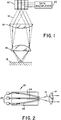
- FIG. 1 is a diagram of a preferred embodiment of multichannel recording apparatus with a laser diode array constructed in accordance with the present invention.
- FIG. 2 is a diagrammatic illustration of the laser diode assembly of FIG. 1 showing the laser diodes edge coupled to channel waveguides.
- FIGS. 3a and 3b are diagrammatic illustrations of the laser diode array of FIG. 1 showing the laser diodes mounted on a silicon substrate.
- FIG. 4 is a diagrammatic view similar to FIGS. 3a and 3b, but illustrating the laser diodes and waveguides on a gallium arsenide substrate.
- FIGS. 5a and 5b illustrate another embodiment of the laser diodes and waveguides on a gallium arsenide substrate similar to FIG. 3, but illustrating a different arrangement of the lasers and waveguides.
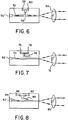
- FIG. 6 illustrates a single laser diode of the laser diode array of FIG. 1 and the associated waveguide to illustrate the signal obtained by a beam splitter.
- FIG. 7 illustrates a single laser diode as does FIG. 6, but illustrating obtaining a signal by coupling from one channel to another using polarization instead of the beam splitter of FIG. 6.
- FIG. 8 is similar to FIGS. 6 and 7, but illustrates a signal obtained by coupling from one channel to another by a tapered edged channel.
- FIG. 9 illustrates an optical system with bulk optics to develop the focus and tracking signals.
- FIG. 10 illustrates another method of obtaining signals wherein reflected light from one channel is reflected into a multimode channel to develop the focus and tracking signals.
- FIG. 11 is similar to FIGS. 9 and 10, but illustrates the use of tapered waveguides for developing signals.
- Referring to FIG. 1, the basic portions of an optical recording and reading system are illustrated. The data to be recorded is first applied to recording circuity (not shown) which encodes the applied data. The encoded data from the recording circuitry is applied to the laser optical system which includes a
multisource array 10. Themultisource array 10 generateslaser beams 12 that are collimated bycollector lens 14 and focused byobjective lens 16 onto the surface of anoptical recording disk 18. The encoded data is coupled to thearray 10 via adata multiplexer 20. The focusedbeam 12 can be regarded as a highly multiplexed data channel with each point in the dynamic image representing an independent data stream so that it is possible to transfer many data channels simultaneously through one optical head in an otherwise conventional optical recording system. - FIGS. 2-5 illustrate various options for the layout of the
multisource array 10 whereby theoptical beams 12 from thediode lasers 22 can be brought closer together to a separation of about 10 µm. In FIG. 2 thediode lasers 22 are edge coupled towaveguides 24. Thewaveguides 24 are curved to bring light beams closer while thediode lasers 22 are separated farther apart. Thewaveguides 24 are preferably constructed of low loss materials so that for a typical propagation distance of about 1 cm, total optical losses are less than about 0.5 decibels. With the proper matching of numerical aperture of laser diodes to numerical aperture of the waveguides, coupling efficiencies of 50 percent or greater can be achieved. It has been experimentally determined that coupling efficiencies of over 30 percent are possible without any anti-reflection coatings on the waveguide surfaces when there is precise alignment of thelaser diodes 22 with thewaveguides 24. - FIGS. 3a and 3b illustrate another embodiment wherein the
waveguides 24′ are fabricated on an oxidized silicon, SiO₂,substrate 26 and thediode lasers 22′ are mounted on asilicon substrate 28. The laser diodes 22' are mounted on thesilicon substrate 28 without a heat sink because thesilicon substrate 28 provides a sufficient heat sink. Each laser diode 22' has a metal contact 30 mounted on thesubstrate 28. The metal contact 30 protrudes through a layer of silicon nitrite, SiN₄, and extends to contact a layer of gallium aluminum arsenide, GaAlAs, 34. The top layer 34 is a layer of gallium arsenide, GaAs, 36 beneath a layer of gallium aluminum arsenide, GaAlAs, 38 which lies below a top layer ofgallium arsenide 40. Again, coupling efficiencies of greater than 50 percent can be achieved by a proper matching of numerical aperture of the waveguide and a precise alignment of the laser diode 22' to the waveguide 24'. Vertical alignment is made easier because thelaser diode 22 is mounted on thesame substrate 28 as the waveguide 24'. - FIG. 4 illustrates another embodiment very similar to FIG. 3 but using a gallium arsenide, GaAs, substrate 28' on which the various layers are grown for fabrication of the
laser diode 22". A diode facet is etched, preferably using a chemical ion beam assisted technique. Using a mask,channel waveguide 24" can be formed in alignment with thelaser diode 22" to couple light from thelaser diode 22" to thechannel waveguide 24". The channel waveguide material may need to be modified slightly, by disordering, for example, to decrease the waveguide loss. The embodiment of FIG. 4 does not require any precise alignment of thelaser diodes 22", and good coupling efficiency, greater than about 60-70 percent, is possible. If the waveguide loss is higher than about 1 decibel per centimeter or otherwise higher than desirable, then during the etching of the laser facets, channels can be etched and dielectric material, such as glass waveguide material, for example, can be used in the channels. - FIGS. 5a and 5b illustrate another embodiment wherein structures are grown on a gallium arsenide, GaAs,
substrate 42 for multichannel recording. Alaser 44 is grown and a facet is etched thereon, then achannel waveguide 46 is formed with a 90° bend. At the bend there is amirror 48 that reflects light over 90° due to total internal reflection. Several channels can be made this way. The channel lengths are preferably short on the order of a few hundred microns so that optical loss is small. An alternative is not to etch a facet on thelaser 44 thereby letting the 90° bent channel act as a laser cavity. Doing this provides minimum alignments and is easier to fabricate. - The above discussion with reference to FIGS. 2-5 has been primarily concerned with the recording channel only. The mechanism for multichannel recording operation includes the plurality of laser diodes wherein each diode is spaced a preselected distance from adjacent diodes and the plurality of channel waveguides that are coupled to the plurality of laser diodes with each channel waveguide then associated with a respective laser diode so that light emitted by the plurality of laser diodes is channeled for convergence at a point outside the waveguides. The preselected spacing of the
laser beams 12 is less than about 50 µm which was heretofore unachievable, and, is preferably about 10 µm. The light emitted by the laser diodes is channeled to the collector lens by the channel waveguides. The channel waveguides define pathways that may vary in length and some of the waveguides may define straight paths and some may define arcuate paths so that the light emitted by the laser diodes converges at some point after exiting the channels. Preferably, the point of convergence is reached by the light beams prior to reaching the collector lens. - The above discussion has been concerned with the recording channel only. This could be useful in high speed writer applications such as a CD high speed writer. For the read channel, the reflected light coming back from the disk surface must be tapped.
- FIGS. 6-8 illustrate apparatus for detecting the light reflected from the disk surface. FIG. 6 illustrates a
laser diode 50 andwaveguide 52 for emitting and channeling light to thelens 54. Abeam splitter 56 directs the reflected beam ontodetectors beam splitter 56 is that there is a loss of light and light gets fed to thediode laser 50 also. FIG. 6 thus illustrates a means for a multichannel reader wherein abeam splitter 56 is positioned in one of the channel waveguides which channel receives reflected light and detector means 58, 60 for detecting light and reflected light by way of thebeam splitter 56. - FIG. 7 illustrates reading apparatus similar to FIG. 6 but using different elements. Light from a
laser diode 62 travels throughchannel waveguide 70 to thecollector lens 72 and reflected back to thechannel waveguide 70. Light is tapped from thechannel 70 by anotherchannel 74 where the light is detected bydetectors second channel 74 for detection purposes. This method requires a quarterwave plate in the optical system and is not suitable for M-O media detection. - In FIG. 8 a tapered
channel 80 is used for detection of reflected light. Light emanating fromlaser diode 82 is channeled throughchannel waveguide 84 to thelens 86 where reflected light from thelens 86 is reflected back to thechannel 82. The taperedchannel 80 directs light todetectors channel waveguide 84 is channeled to thedetectors - FIGS. 6-8 illustrate means for multichannel reading which includes a plurality of detectors that detect reflected light and a plurality of detector waveguides. Each detector waveguide is associated with a selected one of the detectors and is coupled to a selected one of the channel waveguides so that reflected light travelling in the selected channel waveguide is channeled to the selected detector. The means for multichannel reading may include taper coupling and may also include a beam splitter that is positioned in one of the channel waveguides. Detector means are provided for detecting light and reflected light by means of the beam splitter.
- FIGS. 9-11 illustrate apparatus for the detection of tracking and focus signals. FIG. 9 illustrates a bulk optics approach wherein there is one
channel 92 with bulk optics which will do the focus and tracking signal as illustrated. The bulk optics includes acollector lens 94 which receives alight beam 96 from thechannel 92 emitted by thechannel diode 98. Thebeam 96 passes through abeam splitter 100 and a portion of the light travels to thecollector lens 102 where it is directed to the surface of thedisk 104. A portion of the light from thebeam splitter 100 passes throughquarterwave plate 106 and tobeam splitter 108 where light from asecond diode 110 is directed through alens 112 to thesecond beam splitter 108. The output of thebeam splitter 108 is directed to agrating surface 114 and a light therefrom is focused throughlens 116 todetectors 118 for focus and tracking. - Referring now to FIG. 10, another embodiment is illustrated. In this embodiment light reflected from one
channel 120 is reflected into amultimode channel 122 to keep the focus and tracking signal information. Themultimode channel 122 is divided into twochannels multimode waveguide channel 122 for receiving reflected light and a plurality ofdetectors 128 coupled to the mode tomode waveguide channel 122 sufficiently to detect focus and tracking errors. - FIG. 11 also illustrates apparatus for multichannel reading that includes
detectors detector waveguides detector waveguides respective detector channel waveguide channel waveguide 142 is taper coupled todetector waveguide 136, which channels light todetector 130. - It can now be appreciated that there has been presented an apparatus for multichannel recording, multichannel recording and reading, and multichannel recording with focus error and tracking error detection schemes. It can also be appreciated that there has been presented an apparatus for recording onto and reading from an optical disk. The apparatus includes a multisource array that has a plurality of laser diodes which each diode spaced a distance more than about 50 to 100 µm from adjacent diodes. But, the beams emanating from the waveguides are closely spaced less than about 50 µm from one another. This closer spacing is achieved without crosstalk or electro interferences because of a plurality of channel waveguides that are coupled to the laser diodes. Each channel waveguide is associated with a respective laser for directing the light emitted by the diode toward the optical disk for optical recording and it also receives reflected light from the optical disk for reading the optical disk. The arcuate configuration of the waveguides allows beams to be spaced as close as about 10 µm.
- While the invention has been described with particular reference to the preferred embodiments, it will be understood by those skilled in the art that various changes may be made and equivalents may be substituted for elements of the preferred embodiment without departing from invention. In addition, many modifications may be made to adapt a particular situation and material to a teaching of the invention without departing from the essential teachings of the present invention.
- As is evident from the foregoing description, certain aspects of the invention are not limited to the particular details of the examples illustrated, and it is therefore contemplated that other modifications and applications will occur to those skilled in the art. It is accordingly intended that the claims shall cover all such modifications and applications as do not depart from the true spirit and scope of the invention.
Claims (26)
- A multisource array for directing light to an optical disk for optical recording and receiving reflected light from said optical disk for reading said optical disk, comprising:
means for multichannel recording, including:
a plurality of laser diodes with each diode spaced a preselected distance from adjacent diodes; and
a plurality of channel waveguides coupled to said plurality of laser diodes with each channel waveguide being associated with a respective laser diode so that light emitted by said plurality of laser diodes is channeled for convergence at a point outside of said waveguides. - A multisource array, as set forth in Claim 1, comprising:
means for multichannel reading, including:
a beam splitter positioned in one of said channel waveguides which channel receives reflected light; and
detector means for detecting light and reflected light via said beam splitter. - A multisource array, as set forth in Claim 1, wherein light emanating from a first channel of said plurality of channel waveguides has a first polarization, and wherein a portion of said light is reflected back to a second channel of said plurality of channel waveguides and has a second polarization so that said second channel taps light from said first channel.
- A multisource array, as set forth in Claim 1, comprising:
means for multichannel reading, including:
a plurality of detectors for detecting reflected light;
a plurality of detector waveguides, each detector waveguide being associated with a selected one of said plurality of detectors and being taper coupled to a selected one of said plurality of channel waveguides so that reflected light travelling in said selected channel waveguide is channeled to said selected detector. - A multisource array, as set forth in Claim 1, comprising:
means for detecting errors, including:
a multimode waveguide channel for receiving reflected light; and
a plurality of detectors coupled to said multimode waveguide channel sufficient for detecting focus and tracking errors. - An apparatus for recording onto and reading from an optical disk, comprising:
a laser diode array having a plurality of laser diodes with each diode spaced a preselected distance greater than about 50 µm from adjacent diodes and having a plurality of channel waveguides coupled to said plurality of laser diodes, with each channel waveguide being associated with a respective laser, for directing light emitted by said plurality of laser diodes toward said optical disk for optical recording and for receiving reflected light from said optical disk for reading said optical disk, each of said channel waveguides spaced a preselected distance less than about 50 µm from adjacent waveguides. - An apparatus for recording onto and reading from an optical disk, comprising:
a plurality of laser diodes with each diode spaced a preselected distance from adjacent diodes; and
a plurality of channel waveguides coupled to said plurality of laser diodes with each channel waveguide being associated with a respective laser diode so that light emitted by said plurality of laser diodes is channeled for convergence at a point outside of said waveguides. - An apparatus, as set forth in Claim 7, wherein said preselected distance is greater than about 50 µm.
- An apparatus, as set forth in Claim 7, wherein each of channel waveguides is spaced from adjacent waveguides a preselected distance is less than about 50 µm.
- An apparatus, as set forth in Claim 7, wherein said apparatus has a collector lens and wherein light emitted by said plurality of laser diodes is channeled to said collector lens.
- An apparatus, as set forth in Claim 10, wherein said light emitted by said plurality of laser diodes converges prior to reaching said collector lens.
- An apparatus, as set forth in Claim 7, wherein at least one of said channel waveguides defines an arcuate pathway for light travelling from one of said laser diodes to said point of convergence.
- An apparatus, as set forth in Claim 7, wherein said channel waveguides define pathways of various lengths.
- An apparatus, as set forth in Claim 7, wherein at least one of said channel waveguides defines an angled pathway for light travelling from one of said laser diodes and contains a mirror at the angle to reflect light to said point of convergence.
- An apparatus, as set forth in Claim 14, wherein said laser diode has an etched facet.
- An apparatus, as set forth in Claim 14, wherein said angled channel acts as a laser cavity.
- An apparatus, as set forth in Claim 14, wherein said angled channel is spaced a preselected distance from said laser diode.
- An apparatus, as set forth in Claim 7, including a substrate, said waveguides being formed on said substrate and said diodes being mounted on said substrate.
- An apparatus, as set forth in Claim 18, wherein said substrate is an oxidized silicon wafer.
- An apparatus, as set forth in Claim 7, including a substrate, said waveguides being formed on said substrate and said diodes being formed on said substrate.
- An apparatus, as set forth in Claim 20, wherein said substrate is a GaAs substrate.
- An apparatus, as set forth in Claim 7, wherein a portion of said light is reflected back to said plurality of channel waveguides and including:
a detector for detecting reflected light;
a detector waveguide taper coupled to a selected one of said plurality of channel waveguides so that reflected light travelling in said channel waveguide is channeled to said detector. - An apparatus, as set forth in Claim 22, wherein there are a plurality of detectors sufficient for developing error signals.
- An apparatus, as set forth in Claim 7, wherein a portion of said light is reflected back to one channel of said plurality of channel waveguides and including:
a beam splitter in said channel waveguide; and
detector means for detecting light and reflected light via said beam splitter. - An apparatus, as set forth in Claim 7, wherein light emanating from a first channel of said plurality of channel waveguides has a first polarization, and wherein a portion of said light is reflected back to a second channel of said plurality of channel waveguides and has a second polarization so that said second channel taps light from said first channel.
- An apparatus, as set forth in Claim 7, wherein a portion of said light is reflected back to said plurality of channel waveguides and including:
a multimode waveguide channel; and
a plurality of detectors coupled to said multimode waveguide channel sufficient for developing error signals.
Applications Claiming Priority (2)
| Application Number | Priority Date | Filing Date | Title |
|---|---|---|---|
| US787159 | 1991-11-04 | ||
| US07/787,159 US5195152A (en) | 1991-11-04 | 1991-11-04 | Multichannel optical recording apparatus employing laser diodes |
Publications (2)
| Publication Number | Publication Date |
|---|---|
| EP0541461A2 true EP0541461A2 (en) | 1993-05-12 |
| EP0541461A3 EP0541461A3 (en) | 1993-06-30 |
Family
ID=25140601
Family Applications (1)
| Application Number | Title | Priority Date | Filing Date |
|---|---|---|---|
| EP19920420390 Withdrawn EP0541461A3 (en) | 1991-11-04 | 1992-10-29 | Multichannel optical recording apparatus employing laser diodes |
Country Status (3)
| Country | Link |
|---|---|
| US (1) | US5195152A (en) |
| EP (1) | EP0541461A3 (en) |
| JP (1) | JPH05217194A (en) |
Cited By (2)
| Publication number | Priority date | Publication date | Assignee | Title |
|---|---|---|---|---|
| EP0836738A1 (en) * | 1995-07-05 | 1998-04-22 | Yenploy Pty. Ltd. | Optical storage system |
| WO2005027107A1 (en) * | 2003-09-18 | 2005-03-24 | Koninklijke Philips Electronics N.V. | Information carrier and system for reading data stored on such an information carrier |
Families Citing this family (24)
| Publication number | Priority date | Publication date | Assignee | Title |
|---|---|---|---|---|
| US5289454A (en) * | 1991-12-19 | 1994-02-22 | Minnesota Mining And Manufacturing Company | Optical disc addressing devices a method of use thereof |
| US5278812A (en) * | 1992-02-18 | 1994-01-11 | At&T Bell Laboratories | Tracking and focussing functions in optical disk apparatus |
| EP0620458A4 (en) * | 1992-09-07 | 1995-02-01 | Nippon Kogaku Kk | Optical waveguide device and optical instrument using the same. |
| US5617500A (en) * | 1994-05-20 | 1997-04-01 | Nikon Corporation | System for detecting an optical information and scanning microscope system |
| US5835458A (en) * | 1994-09-09 | 1998-11-10 | Gemfire Corporation | Solid state optical data reader using an electric field for routing control |
| GB2312968B (en) * | 1996-05-09 | 2000-09-13 | Daewoo Telecom Ltd | Splicer for light waveguides |
| KR100243134B1 (en) * | 1997-08-30 | 2000-02-01 | 윤종용 | Optical pickup device for recording and reproducing |
| US6341118B1 (en) * | 1998-06-02 | 2002-01-22 | Science Applications International Corporation | Multiple channel scanning device using oversampling and image processing to increase throughput |
| US6166756A (en) * | 1998-06-02 | 2000-12-26 | Science Applications International Corporation | Multiple channel data writing device |
| US6246658B1 (en) | 1998-06-02 | 2001-06-12 | Science Applications International Corporation | Multiple channel scanning device using optoelectronic switching |
| US6091067A (en) * | 1998-06-02 | 2000-07-18 | Science Applications International Corporation | Scanning device using fiber optic bimorph |
| US6584052B1 (en) | 1998-06-02 | 2003-06-24 | Science Applications International Corporation | Method and apparatus for controlling the focus of a read/write head for an optical scanner |
| US6137105A (en) | 1998-06-02 | 2000-10-24 | Science Applications International Corporation | Multiple parallel source scanning device |
| EP1376179A3 (en) * | 2002-06-27 | 2004-04-14 | Toyoda Koki Kabushiki Kaisha | Laminated optical waveguide array, optical beam collecting device and laser emission device |
| US6999484B2 (en) | 2003-03-18 | 2006-02-14 | Eastman Kodak Company | Parallel access data storage system using a combination of VCSEL arrays and an integrated solid immersion lens array |
| JP4792011B2 (en) * | 2007-06-29 | 2011-10-12 | 日本放送協会 | Optical head and optical disk recording / reproducing apparatus |
| US8248905B2 (en) | 2010-10-15 | 2012-08-21 | General Electric Company | Method of parallel bit-wise holographic data storage source using a parallel light source |
| US8154975B1 (en) | 2010-11-18 | 2012-04-10 | General Electric Company | Servoing system for multiple spot registration for holographic replication system |
| US8254224B2 (en) | 2010-11-18 | 2012-08-28 | General Electric Company | Servoing system for master with parallel tracks in a holographic replication system |
| SG185912A1 (en) * | 2011-05-18 | 2012-12-28 | Agency Science Tech & Res | Alignment method for a silicon photonics packaging |
| WO2013136393A1 (en) * | 2012-03-16 | 2013-09-19 | 日本電気株式会社 | Polarization combiner and separator, polarization combining and separating structure, light mixer, optical modulator module, and method for manufacturing polarization combiner and separator |
| US20150205047A1 (en) * | 2012-07-17 | 2015-07-23 | Nec Corporation | Polarization separator, polarization separation structure, optical mixer, and method for manufacturing polarization separator |
| US9196278B1 (en) | 2014-05-23 | 2015-11-24 | Seagate Technology Llc | Laser array for heat assisted magnetic recording |
| CN107924027B (en) | 2015-06-12 | 2024-01-23 | 加利福尼亚太平洋生物科学股份有限公司 | Integrated target waveguide device and system for optical coupling |
Citations (4)
| Publication number | Priority date | Publication date | Assignee | Title |
|---|---|---|---|---|
| EP0092420A1 (en) * | 1982-04-19 | 1983-10-26 | Xerox Corporation | Information storage systems |
| US4428647A (en) * | 1982-11-04 | 1984-01-31 | Xerox Corporation | Multi-beam optical system using lens array |
| EP0345232A2 (en) * | 1988-05-31 | 1989-12-06 | Nikon Corporation | Integrated optical device for magneto-optical recording and reading head |
| US4897671A (en) * | 1989-01-23 | 1990-01-30 | Polaroid Corporation | Integrated optic print head |
Family Cites Families (4)
| Publication number | Priority date | Publication date | Assignee | Title |
|---|---|---|---|---|
| US4318058A (en) * | 1979-04-24 | 1982-03-02 | Nippon Electric Co., Ltd. | Semiconductor diode laser array |
| NL8103599A (en) * | 1981-07-30 | 1983-02-16 | Philips Nv | DEVICE FOR OPTICAL SCANNING OF A DOCUMENT. |
| JP2701403B2 (en) * | 1988-12-29 | 1998-01-21 | ソニー株式会社 | Magneto-optical disk device |
| US5109447A (en) * | 1991-03-04 | 1992-04-28 | The Boeing Company | High-powered, spectrally flat, very broadband optical source including optical coupler and method using same |
-
1991
- 1991-11-04 US US07/787,159 patent/US5195152A/en not_active Expired - Lifetime
-
1992
- 1992-10-29 EP EP19920420390 patent/EP0541461A3/en not_active Withdrawn
- 1992-11-04 JP JP4295227A patent/JPH05217194A/en not_active Withdrawn
Patent Citations (4)
| Publication number | Priority date | Publication date | Assignee | Title |
|---|---|---|---|---|
| EP0092420A1 (en) * | 1982-04-19 | 1983-10-26 | Xerox Corporation | Information storage systems |
| US4428647A (en) * | 1982-11-04 | 1984-01-31 | Xerox Corporation | Multi-beam optical system using lens array |
| EP0345232A2 (en) * | 1988-05-31 | 1989-12-06 | Nikon Corporation | Integrated optical device for magneto-optical recording and reading head |
| US4897671A (en) * | 1989-01-23 | 1990-01-30 | Polaroid Corporation | Integrated optic print head |
Non-Patent Citations (6)
| Title |
|---|
| APPLIED PHYSICS LETTERS vol. 41, no. 1, 1 July 1982, pages 9 - 11 VAN DER ZIEL ET AL 'A closely spaced (50um) array of 16 individually addressable buried hetrostructure GaAs lasers' * |
| JOURNAL OF ELECTRONIC ENGINEERING vol. 24, no. 248, August 1987, TOKYO, JAPAN pages 54 - 56 YAMAGUCHI 'Monolithic 3-Beam Semiconductor Laser: Now a Practical Reality' * |
| OPTICAL ENGINEERING vol. 22, no. 4, July 1983, pages 464 - 472 KOWALSKI ET AL 'Multichannel digital optical disk memory system' * |
| PATENT ABSTRACTS OF JAPAN vol. 12, no. 339 (P-757)12 September 1988 & JP-A-63 098 611 ( ASAHI GLASS CO ) 30 April 1988 * |
| PATENT ABSTRACTS OF JAPAN vol. 14, no. 366 (P-1089)8 August 1990 & JP-A-02 135 306 ( NIPPON TELEGRAPH & TELEPHONE CORP ) 24 May 1990 * |
| SPIE PRO.421, 156 1983, pages 156 - 162 RENO 'Optical disk recording techniques for data rates beyond 100Mbps' * |
Cited By (3)
| Publication number | Priority date | Publication date | Assignee | Title |
|---|---|---|---|---|
| EP0836738A1 (en) * | 1995-07-05 | 1998-04-22 | Yenploy Pty. Ltd. | Optical storage system |
| EP0836738A4 (en) * | 1995-07-05 | 1999-09-22 | Yenploy Pty Ltd | Optical storage system |
| WO2005027107A1 (en) * | 2003-09-18 | 2005-03-24 | Koninklijke Philips Electronics N.V. | Information carrier and system for reading data stored on such an information carrier |
Also Published As
| Publication number | Publication date |
|---|---|
| JPH05217194A (en) | 1993-08-27 |
| EP0541461A3 (en) | 1993-06-30 |
| US5195152A (en) | 1993-03-16 |
Similar Documents
| Publication | Publication Date | Title |
|---|---|---|
| US5195152A (en) | Multichannel optical recording apparatus employing laser diodes | |
| US7184386B2 (en) | Integrated type optical head with sheet waveguide and light coupler | |
| EP0614098B1 (en) | Optical device | |
| US4779259A (en) | Optical head assembly with efficient light source coupling surface and method of construction | |
| US5195150A (en) | Optoelectronic device for outfeed and infeed of radiation | |
| US4945525A (en) | Optical information processing apparatus | |
| US6487224B1 (en) | Laser diode assembly | |
| EP0814468B1 (en) | Optical recording and reproducing device | |
| US5235589A (en) | Apparatus for recording and reproducing optical information and prism coupler | |
| KR100313298B1 (en) | Optics | |
| EP0483438B1 (en) | Integrated optical head structure | |
| EP1184848B1 (en) | Optical pickup apparatus having an improved holographic unit, and optical disk drive including the same | |
| KR20000022892A (en) | Optical head, recording and/or reproducing apparatus, and optical disc drive | |
| JPS6273437A (en) | Optical head device | |
| US5161148A (en) | Optical pick-up using wavelength guide with grating coupler therein | |
| KR100456984B1 (en) | Semiconductor laser device | |
| US5781576A (en) | Semiconductor laser device and optical disk drive | |
| KR20010085724A (en) | Semiconductor laser apparatus, laser coupler, data reproduction apparatus, data recording apparatus and production method of semiconductor laser apparatus | |
| US5801880A (en) | Confocal microscope with optical recording and reproducing apparatus | |
| US5233595A (en) | Optical pickup including waveguide light intensity detection means for controlling a position/intensity of a semiconductor laser | |
| US6408116B1 (en) | Light guide path element and optical pickup | |
| US5757029A (en) | Triangular pyramidal semiconductor structure and optical device using the same | |
| JPH06111362A (en) | Mutichannel optical laser system, data reading method and multichannel beam deflector | |
| KR100293464B1 (en) | optical source module for generating beams different from the wave length and method for fabricating the same and optical pick-up apparatus using the same | |
| JPS62275332A (en) | Optical head |
Legal Events
| Date | Code | Title | Description |
|---|---|---|---|
| PUAI | Public reference made under article 153(3) epc to a published international application that has entered the european phase |
Free format text: ORIGINAL CODE: 0009012 |
|
| PUAL | Search report despatched |
Free format text: ORIGINAL CODE: 0009013 |
|
| AK | Designated contracting states |
Kind code of ref document: A2 Designated state(s): DE FR GB |
|
| AK | Designated contracting states |
Kind code of ref document: A3 Designated state(s): DE FR GB |
|
| 17P | Request for examination filed |
Effective date: 19931210 |
|
| 17Q | First examination report despatched |
Effective date: 19951219 |
|
| STAA | Information on the status of an ep patent application or granted ep patent |
Free format text: STATUS: THE APPLICATION IS DEEMED TO BE WITHDRAWN |
|
| 18D | Application deemed to be withdrawn |
Effective date: 19960430 |