EP0540948A2 - Regulated charge pump and method therefor - Google Patents
Regulated charge pump and method therefor Download PDFInfo
- Publication number
- EP0540948A2 EP0540948A2 EP92118084A EP92118084A EP0540948A2 EP 0540948 A2 EP0540948 A2 EP 0540948A2 EP 92118084 A EP92118084 A EP 92118084A EP 92118084 A EP92118084 A EP 92118084A EP 0540948 A2 EP0540948 A2 EP 0540948A2
- Authority
- EP
- European Patent Office
- Prior art keywords
- voltage
- terminal
- power supply
- transistor
- supply voltage
- Prior art date
- Legal status (The legal status is an assumption and is not a legal conclusion. Google has not performed a legal analysis and makes no representation as to the accuracy of the status listed.)
- Granted
Links
Images

Classifications
-
- H—ELECTRICITY
- H02—GENERATION; CONVERSION OR DISTRIBUTION OF ELECTRIC POWER
- H02M—APPARATUS FOR CONVERSION BETWEEN AC AND AC, BETWEEN AC AND DC, OR BETWEEN DC AND DC, AND FOR USE WITH MAINS OR SIMILAR POWER SUPPLY SYSTEMS; CONVERSION OF DC OR AC INPUT POWER INTO SURGE OUTPUT POWER; CONTROL OR REGULATION THEREOF
- H02M3/00—Conversion of dc power input into dc power output
- H02M3/02—Conversion of dc power input into dc power output without intermediate conversion into ac
- H02M3/04—Conversion of dc power input into dc power output without intermediate conversion into ac by static converters
- H02M3/06—Conversion of dc power input into dc power output without intermediate conversion into ac by static converters using resistors or capacitors, e.g. potential divider
- H02M3/07—Conversion of dc power input into dc power output without intermediate conversion into ac by static converters using resistors or capacitors, e.g. potential divider using capacitors charged and discharged alternately by semiconductor devices with control electrode, e.g. charge pumps
Definitions
- This invention relates generally voltage generator circuits, and more particularly, to regulated charge pump circuits.
- EEPROMs electrically erasable programmable read only memories
- An internal charge pump circuit increases the power supply voltage to the desired programming voltage.
- a conventional technique to increase the internal voltage is to use a voltage multiplier circuit. The voltage multiplier circuit is based on a charging capacitor and two phases of a clock. During one clock phase, the power supply voltage is applied to a first terminal of the charging capacitor while a second terminal is grounded. Then, during the second phase, the power supply voltage source is isolated from the first terminal of the charging capacitor. The second terminal is disconnected from ground, and the power supply voltage is applied to the second terminal.
- the first terminal of the charging capacitor is boosted to a voltage of twice the power supply voltage referenced to ground.
- This voltage, at the first terminal of the charging capacitor, is then used to charge a holding capacitor.
- the first terminal of the charging capacitor is isolated from the holding capacitor and is again coupled to the power supply voltage.
- the voltage of the holding capacitor provides the charge-pumped voltage.
- This example demonstrated a voltage multiplier with an integer multiple of two; in the absence of loading, the charge-pumped voltage is equal to twice the power supply voltage.
- Other charge pump circuits have two such charge pumps connected in series to provide a voltage multiplier with an integer multiple of four.
- a voltage-multiplying charge pump circuit may be useful also in battery-based systems. Since the battery voltage may be low, a charge pump circuit may be used to increase the voltage to internal circuitry. However, this creates problems.
- a battery voltage may vary widely between the time it is first used (either a new battery or a newly-recharged battery) and the time it goes dead. For example, three type AA batteries may be used to form a power supply with a nominal voltage of 3.75 volts, which is usually acceptable for integrated circuits which use the conventional +5.0 volt power supply. Before going dead, the battery voltage may fall to approximately 2.7 volts. Thus, a voltage-doubling charge pump circuit could be used to increase the 2.7-volt power supply voltage to 5.4 volts.
- each battery voltage may be as much as 1.8 volts, and the charge-pumped power supply voltage would be unacceptably high.
- a voltage doubling charge pump would provide voltages between 10.8 and 5.4 volts between recharges.
- a 10.8-volt power supply is harmful because reliability could be reduced in circuits designed to work at 5.0 volts.
- CMOS complementary metal-oxide-semiconductor
- gate rupture and latchup may occur.
- a clamping device such as a Zener diode, could be used to reduce the output voltage.
- the clamping device sinks current during the period of excess voltage to drop the voltage to the required level.
- shunt regulation methods may be used to reduce the output voltage.
- the charge pump wastes current through the Zener diode or regulation device. As more current is wasted, battery life shortens.
- techniques other than the use of passive devices to limit the voltage are needed.
- a regulated charge pump comprising a charge pump core, proportional means, and integrating means.
- the charge pump core boosts a voltage existing at a first terminal of a capacitor during a first predetermined time period, by an amount equal to a first power supply voltage referenced to a second power supply voltage, and provides a regulated charge-pumped voltage in response.
- the proportional means changes the voltage proportionately in response to a difference between a reference voltage and a proportional voltage, the proportional voltage being a predetermined fraction of the charge-pumped voltage, the predetermined fraction making the proportional voltage equal to the reference voltage when the regulated charge-pumped voltage is equal to a desired value.
- the integrating means further changes the first voltage proportionately in response to an integration of a difference between the proportional voltage and the reference voltage.
- a method of providing a regulated charge-pumped voltage comprising the steps of providing a charging capacitor; alternately, coupling a second terminal of the charging capacitor to a first power supply voltage terminal, or coupling the second terminal of the charging capacitor to a second power supply voltage terminal, respectively in response to first and second non-overlapping clock signals; providing the regulated charge-pumped voltage in response to a first voltage at a first terminal of the charging capacitor; forming a second voltage proportional to the regulated charge-pumped voltage; comparing the second voltage to a reference voltage; biasing a first transistor, coupled between the first power supply voltage terminal and a first terminal of the capacitor, to be conductive proportionally to the comparison of the second voltage to the reference voltage; integrating a difference between the second voltage and the reference voltage; and biasing a second transistor, coupled between the first power supply voltage terminal and the first terminal of the charging capacitor, to be conductive proportionally to the integrated difference.
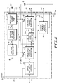
- FIG. 1 illustrates in block form a digital cordless telephone handset utilizing a mixed signal processing system in accordance with the present invention.
- FIG. 2 illustrates in partial block form and partial schematic form the mixed signal processing system of FIG. 1.
- FIG. 3 illustrates in partial block form and partial schematic form the PCM codec of FIG. 2.
- FIG. 4 illustrates in partial schematic form and partial block form the regulated charge pump of FIG. 2 in accordance with the present invention.
- FIG. 5 illustrates in partial schematic form and partial block form the bias circuit used in the regulated charge pump of FIG. 4.
- FIG. 1 illustrates in block form a digital cordless telephone handset 20 utilizing a mixed signal processing system 22 in accordance with the present invention.
- Handset 20 implements a standard protocol, such as the U.K. Cordless Telephone, Second Generation (CT-2) or the Digital European Cordless Telephone (DECT) standard.
- CT-2 protocol telephone signals are received and transmitted digitally in packets in a half-duplex or ping-pong scheme between handset 20 and a base station (not shown in FIG. 1).
- An antenna 24 is used for transmitting and receiving radio-frequency (RF) representations of telephonic signals.
- An RF system 25 is connected to antenna 24 for receiving and demodulating, and transmitting and modulating, digital streams of telephonic data.
- RF radio-frequency
- signal refers to a time-varying electrical signal
- digital signal refers to a series of digital samples of the signal
- a "packet” includes a portion of the digital signal, or alternatively, a specified number of digital samples of the telephone signal, along with digital signalling bits.
- a packet from the base station is received as a modulated RF signal on antenna 24.
- Radio frequency system 25 receives the RF signal and demodulates it.
- the modulation scheme is a two-level FSK shaped by an approximately Gaussian filter, as described in the CT-2 Common Air Interface Specification.
- the packet is then presented to a time division duplex block 26.
- Time division duplex block 26 splits the packet into its two constituent components, making the signalling bits available to microprocessor 27.
- Time division duplex block 26 makes the compressed digital signal available to mixed signal processing system 22 through input and output signals 32a.
- microprocessor 27 reads the signalling bits and performs associated signalling functions, such as call setup and disconnect.
- ADPCM transcoder 28 decompresses the compressed digital signal received from time division duplex block 26 by a conventional algorithm, such as the CCITT Recommendation G.721 or the American National Standard T1.301-1988. When decompressed, the digital signal exists as digital PCM data compressed by a conventional algorithm such as A-law or m-law.
- ADPCM transcoder is connected via input and output signals 32b to microprocessor 27. Microprocessor 27 initializes and controls the operation of ADPCM transcoder 28 through input and output signals 32b.
- PCM codec 29 receives the PCM data via input and output signals 33, performs A-law or m-law decompression to form an analog telephone signal, and provides the analog telephone signal to a speaker 31 and a ringer (not shown in FIG. 1) via output signals 35. Additional interface circuitry between ADPCM transcoder 28 and PCM codec 29 is not shown in FIG. 1.
- a microphone 30 provides an analog telephone signal via input signal lines 34 to PCM codec 29.
- PCM codec 29 converts the analog telephone signal to a digital telephone signal and compresses it according to the A-law or m-law algorithm, and provides the digital telephone signal to ADPCM transcoder 28 via input and output signals 33.
- ADPCM transcoder 28 in turn compresses the digital telephone signal according to the conventional algorithm (such as the CCITT G.721 or ANSI T1.301-1988 standard) and provides the compressed digital signal to time division duplex block 26.
- Time division duplex block 26 then combines signalling bits from microprocessor 27 with the compressed digital data from APDCM transcoder 28 to form a CT-2 packet.
- Time division duplex block 26 provides the CT-2 packet to radio frequency system 25, which modulates it and provides it as an RF signal to antenna 24, where it is radiated and eventually received by the base station.
- PCM codec 29 performs the function of a conventional integrated circuit, such as the Motorola MC145554 m-law PCM Codec-Filter or the Motorola MC145557 A-law PCM Codec-Filter.
- ADPCM transcoder 28 also performs the function of a conventional integrated circuit, such as the Motorola MC145532 ADPCM Transcoder.
- PCM codec filter 29 is primarily analog, while ADPCM transcoder 28 is primarily digital; however, mixed signal processing system 22 is required to operate from a single battery power supply formed typically by three type AA batteries (not shown in FIG. 1). Mixed signal processing system 22 must operate on battery voltages varying from 2.7 volts to 5.25 volts and still meet the CT-2 specification. At the same time, power consumption must be kept to a minimum in order to maximize battery life. ADPCM transcoder 28 must perform its operation within the time required to process packets to operate on continuous, real-time speech signals. Also, reliable operation is required. Thus, a new approach which solves these problems is needed. Mixed signal processing system 22 satisfies these requirements as is now illustrated with reference to FIG. 2.
- FIG. 2 illustrates in partial block form and partial schematic form mixed signal processing system 22 of FIG. 1.
- Mixed signal processing system 22 includes ADPCM transcoder 28 and PCM codec filter 29 as previously illustrated in FIG. 1.
- mixed signal processing system 22 includes a power supply subsystem 40 having a voltage regulator 41, a bandgap voltage reference 42, and a regulated charge pump 43, a level shifter 44, and several power supply terminals and signal lines.
- the terminals include a terminal 70 for receiving a voltage labelled "V BAT ", a terminal 71 for receiving a voltage labelled "V SS ", a first capacitor terminal 72, a second capacitor terminal 73, and a third capacitor terminal 74.
- the signal lines include input and output signal lines 32, input signal lines 34, output signal lines 34', and input and output signal lines 35'.
- Signal lines corresponding to signal lines in FIG. 1 are given the same reference number.
- input and output signal lines 32 of FIG. 2 include input and output signal lines 32a and 32b as previously illustrated in FIG. 1, and input and output signal lines 35' include output signal line 35 of FIG. 1 and other input and output signal lines not shown in FIG. 1.
- ADPCM transcoder 28 includes input and output buffers 50, and a three-volt digital subsystem 51.
- PCM codec 29 includes a five-volt analog subsystem 60, and a battery-powered analog subsystem 61.
- a first capacitor 80 is connected between terminals 72 and 73, and a second capacitor 81 is connected between terminals 74 and 71.
- V BAT is a battery voltage provided by, for example, three type AA nicad batteries (not shown in FIG. 2) having a nominal voltage of 3.75 volts but varying between 2.7 and 5.4 volts between recharges.
- V SS is a common, or ground power supply voltage having a nominal value of zero volts.
- bandgap voltage reference 42 is connected to V BAT and V SS and provides a stable, precise voltage labelled "V REF " in response.
- Bandgap voltage reference 42 is a bandgap voltage reference circuit which is able to operate at power supply voltages down to approximately 2.7 volts.
- Voltage regulator 41 is connected between V BAT and V SS , and receives voltage V REF to provide an internal reference.
- Voltage regulator 41 is a conventional CMOS voltage regulator which provides a regulated output voltage, labelled "V DSP ".
- V DSP has a nominal value of 3.0 volts which remains substantially constant with variations in V BAT until V BAT approaches 3.0 volts. As V BAT falls below 3.0 volts (when the voltage of the nicad batteries falls due to discharge), V DSP likewise compresses.
- Power supply subsystem 40 also includes regulated charge pump 43, which is connected between V BAT and V SS .
- Regulated charge pump 43 is connected to the first terminal of first capacitor 80 via terminal 72, to the second terminal of first capacitor 80 via terminal 73, and to the first terminal of second capacitor 81 via terminal 74, receives voltage V REF and a clock signal labelled "CLOCK", and provides an output voltage labelled V DD .
- Regulated charge pump 43 combines two conventional functions. First, regulated charge pump 43 increases the voltage of V BAT through clocked capacitive charge pumping. In a preferred embodiment, mixed signal processing system 22 is included in a single monolithic integrated circuit. Capacitors 80 and 81 are too large to be provided monolithically and thus are external to the integrated circuit. Second, regulated charge pump 43 regulates the charge-pumped voltage to provide a voltage labelled "V DD ".
- V DD has a nominal voltage of approximately 5.0 volts, but remains substantially constant as V BAT changes (due to the regulation).
- ADPCM transcoder 28 is a conventional ADPCM transcoder modified to separate internal circuitry in accordance with differing power supply requirements.
- input and output buffers 50 are separated from three-volt digital subsystem 51 and are connected between V BAT and V SS , and provide and receive signals via input and output signal lines 32.
- Three-volt digital subsystem 51 performs all the functions of a conventional ADPCM transcoder except for the functions provided by input and output buffers 50.
- Subsystem 51 is connected between V DSP and V SS , connects to input and output buffers 50, receives input signals from five-volt analog subsystem 60, and provides output signals to level shifter 44 via signal lines 33b, one of which is signal CLOCK, which is also provided to regulated charge pump 43.
- Level shifter 44 receives power supply voltages V DSP and V DD and is coupled to V SS , and level shifts the signals conducted on signal lines 33b and provides corresponding signals 33c to subsystem 60.
- PCM codec 29 is a conventional PCM codec modified to separate internal circuitry in accordance with differing power supply requirements. In PCM codec 29, five-volt analog subsystem 60 performs all the functions of a conventional PCM codec except the special functions performed by subsystem 61 as described below.
- Subsystem 60 is connected between V DD and V SS , receives a microphone signal via input signal lines 34, and connects to subsystem 51 via signal lines 33a.
- Battery-powered analog subsystem 61 is connected between V BAT and V SS and is connected to input and output signal lines 35'.
- Mixed signal processing system 22 has several advantages over known mixed signal processing systems.
- Voltage regulator 41 provides a power supply voltage, V DSP , to subsystem 51 which is substantially constant with respect to changes in V BAT .
- V DSP power supply voltage
- subsystem 51 uses CMOS digital logic.
- CMOS logic circuitry may be designed to operate at high speed and low power supply voltage, such as at 3.0 volts.
- circuitry consumes large amounts of power when the power supply voltage is increased to around 4.0 or 5.0 volts, and in addition, integrated circuit area increases due to a need for additional area for power supply busses. At reduced power consumption levels, junction temperatures are reduced; thus, integrated circuit packaging specifications may be relaxed and reliability is enhanced.
- An added benefit is that digital subsystem 51 is designed to operate within a narrow range of power supply voltages, simplifying circuit design.
- mixed signal processing system 22 performs analog functions reliably despite changes in V BAT .
- Regulated charge pump 43 provides a power supply voltage, V DD , having a voltage high enough for desired analog operation.
- V DD voltage high enough for desired analog operation.
- analog circuitry in analog subsystem 60 has sufficient headroom to operate linearly.
- harmfully high voltages provided by conventional integer charge pumping are avoided.
- V BAT voltage range
- a standard 2X integer charge pump were used to power the analog circuitry, then the voltage range would be from 5.4 to about 10.8 volts. At the high end of the range, reliability is reduced.
- mixed signal processing system 22 reliably interfaces to external circuitry.
- Mixed signal processing system 22 separates input and output buffers 50 from digital subsystem 51. While digital subsystem 51 is connected to V DSP , input and output buffers 50 are connected between V BAT and V SS . Thus, logic high output signal levels of input and output buffers 50 correspond to the output signal levels of other devices, such as microprocessor 27. As illustrated in FIG. 1, ADPCM codec 28 is connected both to time division duplex block 26 and to microprocessor 27. Internally, level shifter 44 similarly increases the logic levels of digital signals provided by digital subsystem 51 to analog subsystem 60.
- mixed signal processing system 22 reduces power consumption by powering analog subsystem 60 from V DD and battery-powered output subsystem 61 from V BAT .
- Circuitry in analog subsystem 61 includes drivers which require a high current drive.
- subsystem 61 includes drivers to provide analog outputs to speaker 31 of FIG. 1. By separating the circuitry, efficiency losses introduced by regulated charge pump 43 do not include losses from the high current drivers.
- FIG. 3 illustrates in partial block form and partial schematic form PCM codec 29. Illustrated in FIG. 3 is analog subsystem 60 and battery-powered analog subsystem 61, which includes amplifiers 100, 101, and 102.
- Analog subsystem 60 provides receive analog output signals labelled "RO", "AXI+", and "AXI-”.
- AXI+ and AXI- form a differential representation of the analog output signal.
- amplifier 100 is a differential amplifier which receives signals AXI+ and AXI- on input terminals and provides a signal labelled "AXO+” on a positive output terminal thereof, and a signal labelled "AXO-" on a negative output terminal thereof.
- Amplifier 101 is an operational amplifier which receives an input signal labelled "PI" on a negative input terminal thereof, a signal voltage labelled “V AG " on a positive input terminal thereof, and provides a signal labeled "PO-".
- V AG is an analog ground reference voltage which has a value of approximately V BAT /2.
- Amplifier 102 is an inverting amplifier which receives signal PO- on an input terminal thereof, and provides a signal labelled "PO+” on an output terminal thereof. Signals AXO+ and AXO- may be used to drive an output device such as a ringer or the like (not shown in FIG. 1).
- Input signal PI typically receives signal RO and is used with external resistors to set the gain of push-pull signals PO+ and PO- provided by amplifiers 101 and 102.
- Amplifiers 101 and 102 are large enough to drive a telephone handset earpiece or small speaker.
- Powering subsystem 61 from V BAT instead of V DD , reduces power consumption by preventing a large power loss due to the efficiency of regulated charge pump 43 being less than 100%.
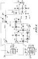
- FIG. 4 illustrates in partial schematic form and partial block form regulated charge pump 43 of FIG. 2 in accordance with the present invention.
- Regulated charge pump 43 includes generally a non-overlapping clock generator circuit 110, a bias circuit 111, a proportional portion 112, an integrating portion 113, and a charge pump core 114.
- Proportional portion 112 includes an amplifier 120, a transmission gate 121, and a P-channel transistor 122.
- Integrating portion 113 includes an amplifier 130, transmission gates 131, 132, and 133, a P-channel transistor 134, a capacitor 135, a transmission gate 136, a capacitor 137, a transmission gate 138, a capacitor 139, transmission gates 140 and 141, and an amplifier 142.
- Charge pump core 114 includes capacitor 80, P-channel transistors 150, 151, and 152, an N-channel transistor 153, a P-channel transistor 154, and capacitor 81.
- Non-overlapping clock circuit 110 receives signal CLOCK, is coupled to power supply voltages V BAT , V DD , and V SS , and provides non-overlapping clock signals labelled "F1", “ F1 ⁇ “, “F2”, and “ F2 ⁇ “, which are level-shifted to V DD .
- Bias circuit 111 is coupled between power supply terminals V BAT and V SS , receives power supply voltage V DD , and provides an output signal labeled "V PDD " and an output signal labeled "PTUBBIAS”.
- amplifier 120 is an operational transconductance amplifier (OTA) having a negative input terminal for receiving signal V REF , a positive input terminal for receiving signal V PDD , and an output terminal for providing a signal labelled "PCNTL".
- Transmission gate 121 has a first current terminal for receiving signal PCNTL, a second current terminal, a positive control terminal for receiving signal F1, and a negative control terminal for receiving signal F1 ⁇ .
- Transistor 122 has a source for receiving power supply voltage V DD , a gate for receiving signal F1, and a drain connected to the second current terminal of transmission gate 121.
- amplifier 130 has a positive input terminal for receiving signal V PDD , a negative input terminal, and an output terminal connected to the negative input terminal of amplifier 130.
- Transmission gate 131 has a first current terminal connected to the output terminal of amplifier 130, a second current terminal, a positive control terminal for receiving signal F2, and a negative control terminal for receiving signal F2 ⁇ .
- Transmission gate 132 has a first current terminal connected to the second current terminal of transmission gate 131, a second current terminal for providing a signal labelled "ICNTL", a positive control terminal for receiving signal F1, and a negative control terminal for receiving signal F1 ⁇ .
- Transmission gate 133 has a first current terminal for receiving signal ICNTL, a second current terminal, a positive control terminal for receiving signal F1, and a negative control terminal for receiving signal F1 ⁇ .
- Transistor 134 has a source for receiving power supply voltage V DD , a gate for receiving signal F1, and a drain connected to the second current terminal of transmission gate 133.
- Capacitor 135 has a first terminal connected to the second current terminal of transmission gate 131, and a second terminal.
- Transmission gate 136 has a first current terminal for receiving signal V REF , a second current terminal, a positive control terminal for receiving signal F1, and a negative control terminal for receiving signal F1 ⁇ .
- Capacitor 137 has a first terminal connected to the second current terminal of transmission gate 136, and a second terminal connected to the second terminal of capacitor 135.
- Transmission gate 138 has a first current terminal connected to the second terminals of capacitors 135 and 137, a second current terminal, a positive control terminal for receiving signal F1, and a negative control terminal for receiving signal F1 ⁇ .
- Capacitor 139 has a first terminal connected to the second current terminal of transmission gate 138, and a second terminal connected to the second current terminal of transmission gate 132.
- Transmission gate 140 has a first current terminal connected to the output terminal of amplifier 130, a second current terminal connected to the second current terminal of transmission gate 136, a positive control terminal for receiving signal F2, and a negative control terminal for receiving signal F2 ⁇ .
- Transmission gate 141 has a first current terminal connected to the output terminal of amplifier 130, a second current terminal connected to the second terminals of capacitors 135 and 137, a positive control terminal for receiving signal F2, and a negative control terminal for receiving signal F2 ⁇ .
- Amplifier 142 has a negative input terminal connected to the second current terminal of transmission gate 138, a positive input terminal connected to the output terminal of amplifier 130, and an output terminal connected to the second current terminal of transmission gate 132 and to the second terminal of capacitor 139.
- transistor 150 has a source connected to V BAT , a gate connected to the second current terminal of transmission gate 121, a drain, and a bulk or well receiving signal PTBUBIAS.
- Transistor 151 has a source connected to V BAT , a gate connected to the second current terminal of transmission gate 133, a drain connected to the drain of transistor 150 at terminal 72, and a bulk or well receiving signal PTUBBIAS.
- Transistor 152 has a first current electrode connected to the drains of transistors 150 and 151, a gate for receiving signal F2 ⁇ , a second current electrode for providing power supply voltage V DD , and a bulk or well receiving signal PTUBBIAS.
- Capacitor 80 has a first terminal connected to terminal 72, and a second terminal connected to terminal 73, as previously illustrated.
- Transistor 153 has a drain connected to the second terminal of capacitor 80 at node 73, a gate for receiving signal F1, and a source connected to V SS .
- Transistor 154 has a source connected to power supply voltage V BAT , a gate for receiving signal F2 ⁇ , a drain connected to the drain of transistor 153, and a bulk or well connected to PTUBBIAS.
- Capacitor 81 has a first terminal connected to the second current electrode of transistor 152 via terminal 74, and a second terminal connected to V SS , as previously illustrated.
- Circuit 110 is a conventional non-overlapping clock generator circuit, which receives signal CLOCK, and provides four clock signals labelled F1, F1 ⁇ , F2, and F2 ⁇ , which are level shifted to V DD . Because of the non-overlap, signal F1 is not the same as signal F2 ⁇ , and signal F2 is not the same as signal F1 ⁇ .
- capacitors 80 and 81 are coupled to regulated charge pump circuit 43 via terminals 72 and 73, and 74 and 71, respectively. Although capacitors 80 and 81 may be viewed as integral parts of regulated charge pump 43, they are preferably external to an integrated circuit which includes regulated charge pump 43 because of their required size. For example, in the illustrated embodiment, capacitors 80 and 81 have values of approximately 0.1 and 1.0 microfarads, respectively, and thus it is impractical to build such capacitors on an integrated circuit.
- Charge pump core 114 uses charging capacitor 80 to provide voltage V DD above voltage V BAT . However, proportional portion 112 and integrating portion 113 alter the operation of charge pump core 114 to integrally regulate V DD .
- transistor 153 is conductive and couples the second terminal of capacitor 80 to V SS . In a conventional charge pump design, a single transistor would also couple the first terminal of capacitor 80 to V BAT during F1.
- F2 ⁇ makes transistor 152 nonconductive, isolating the first terminal of capacitor 81 from V DD .
- V DD is maintained by holding capacitor 81.
- Transistor 154 is also nonconductive.
- transistor 153 is inactive, and transistor 154 is conductive and connects the second terminal of capacitor 80 to V BAT .
- This action boosts the voltage at the first terminal of capacitor 80 to approximately twice V BAT .
- Transistor 152 is also conductive, and the charge stored in capacitor 80 is dumped into holding capacitor 81. At the end of F2, transistor 152 becomes nonconductive and holding capacitor 81 maintains the level of V DD . By repeating this operation, capacitor 81 eventually charges up to approximately twice V BAT .
- transistors 150 and 151 are made conductive in response to signals PCNTL and ICNTL, which are provided by proportional portion 112 and integrating portion 113.
- Amplifiers 120 and 142 have outputs reference to V DD
- amplifier 130 has an output referenced to V BAT .
- Proportional portion 112 makes transistor 150 proportionately conductive in response to a comparison of V PDD and V REF .
- Portion 112 has a fast response to bring V DD to approximately a desired voltage.
- Integrating portion 113 operates somewhat slower to make transistor 151 proportionately conductive to bring V DD very close to the desired value.
- regulated charge pump 43 charge pumps V BAT and regulates the charge-pumped voltage to efficiently provide V DD at the desired voltage (+5.0 volts).
- Bias circuit 111 provides V PDD at a predetermined fraction of a desired value of V DD ; the predetermined fraction is that fraction that makes V PDD equal to V REF when V DD is equal to its desired value.
- the desired value of V DD is +5.0 volts
- the value of V REF is approximately 1.25 volts.
- a fraction of .25 is applied. The accuracy of the fraction is determined by the technique used to generate it, which is described with reference to FIG. 5 below.
- Amplifier 120 compares V REF to V PDD .
- amplifier 120 is an operational transconductance amplifier (OTA), whose output voltage varies in response to a difference in voltage between the positive and negative input terminals.
- the gate of transistor 150 provides a capacitive load, with transistor 122 providing a pullup to V DD .
- transmission gate 121 is active to pass the signal PCNTL at the output of amplifier 120 to the gate of transistor 150.
- Amplifier 120 varies signal PCNTL until the voltages at the positive and negative input terminals are equal; thus, amplifier 120 makes transistor 150 differentially more or less conductive until V DD is approximately equal to its desired voltage.
- Proportional portion 112 operates very quickly in response to changes in load conditions on V DD ; however, amplifier 120 and transmission gate 121 introduce offsets which limit the accuracy of V DD .
- Integrating portion 113 adjusts the conductivity of transistor 151 to further increase the accuracy of V DD .
- Integrating portion 113 is a switched capacitor (switched-C) differential integrator which integrates a difference between V PDD and V REF over time. While slower in response than proportional portion 112, integrating portion 113 includes the history of the signal levels, which eventually cancels the offset error of proportional portion 112.
- Amplifier 130 is a unity-gain differential amplifier which buffers signal V PDD and keeps integrating portion 113 from affecting the operation of proportional portion 112. At power up, signals PCNTL and ICNTL are low in potential, making transistors 150 and 151 strongly conductive to reach the desired value of V DD quicker.
- Regulated charge pump 43 provides V DD at a desired value of approximately 5.0 volts without having to first charge pump the battery voltage to a multiple thereof, and then to regulate or clamp the charge-pumped voltage to a desired, lower voltage. This regulation can be very advantageous for some values of V BAT . For example, immediately after recharge, V BAT may be approximately 5.4 volts.
- a conventional voltage-doubling charge pump circuit provides a voltage of 10.8 volts, which may be harmful to circuitry designed to operate at 5.0 volts. Furthermore, conventional methods of shunt regulation or clamping also waste current. Regulated charge pump 43 provides regulation such that V DD is never doubled. Regulated charge pump 43 also does not use clamping devices such as Zener diodes to limit the output voltage, but rather uses proportional and integrating action to provide V DD with high accuracy and high efficiency.
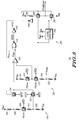
- FIG. 5 illustrates in partial schematic form and partial block form bias circuit 111 used in regulated charge pump 43 of FIG. 4.
- Bias circuit 111 includes generally a first resistor string circuit 200, a second resistor string circuit 210, a comparator 220, a hysteresis control circuit 230, and a bias generator circuit 240.
- First resistor string circuit 200 includes resistors 201 and 202, a transmission gate 203, resistors 204 and 205, and transmission gates 206 and 207.
- Second resistor string circuit 210 includes a resistor 211, transmission gates 212 and 213, and resistors 214 and 215.
- Hysteresis control circuit 230 includes a NOR gate 231 and an inverter 232.
- Bias generator circuit 240 includes a level shifter 243, an inverter 244, a resistor 245, and transmission gates 246 and 247.
- resistor 201 has a first terminal connected to V BAT , and a second terminal.
- Resistor 202 has a first terminal connected to the second terminal of resistor 201, and a second terminal.
- Transmission gate 203 has a first current terminal connected to the second terminal of resistor 202, a second current terminal, a positive control terminal for receiving a signal labeled "PD1", and a negative control terminal for receiving a signal labelled " PD1 ⁇ ".
- Resistor 204 has a first terminal connected to the second current terminal of transmission gate 203, and a second terminal.
- Resistor 205 has a first terminal connected to the second terminal of resistor 204, and a second terminal connected to V SS .
- Transmission gate 206 has a first current terminal connected to the second terminal of resistor 201, a second current terminal, a positive control terminal for receiving a signal labelled "HYST", and a negative control terminal for receiving a signal labelled " HYST ⁇ ".
- Transmission gate 207 has a first current terminal connected to the second terminal of resistor 204, a second current terminal connected to the second current terminal of transmission gate 206, a positive control terminal for receiving signal HYST ⁇ , and a negative control terminal for receiving signal HYST.
- resistor 211 has a first terminal for receiving power supply voltage V DD , and a second terminal.
- Transmission gate 212 has a first current terminal connected to the second terminal of resistor 211, a second current terminal, a positive control terminal for receiving a signal labelled "PD2", and a negative control terminal for receiving a signal labelled PD2 ⁇ .
- Transmission gate 213 has a first current terminal connected to the second current terminal of transmission gate 212, a second current terminal, a positive control terminal for receiving signal PD2, and a negative control terminal for receiving signal PD2 ⁇ .
- Resistor 214 has a first terminal connected to the second current terminal of transmission gate 213, and a second terminal for providing signal V PDD .
- Resistor 215 has a first terminal connected to the second terminal of resistor 214, and a second terminal connected to V SS .
- Comparator 220 has a positive input terminal connected to the second current terminal of transmission gate 206, a negative input terminal connected to the second current terminal of transmission gate 212, and an output terminal for providing a signal labelled "C OUT ".
- NOR gate 231 has a first input terminal for receiving a signal labelled "PD”, a second input terminal connected to the output terminal of comparator 220 for receiving signal C OUT thereon, and an output terminal for providing signal HYST ⁇ .
- Inverter 232 has an input terminal connected to the output terminal of NOR gate 231, and an output terminal for providing signal HYST.
- level shifter 243 is connected to the output terminal of comparator 220, and provides an output signal on an output terminal thereof.
- Inverter 244 has an input terminal connected to the output terminal of level shifter 243, and an output terminal.
- Resistor 245 has a first terminal connected to V BAT , and a second terminal.
- Transmission gate 246 has a first current terminal connected to the second terminal of resistor 245, a second current terminal for providing signal PTUBBIAS, a positive control terminal connected to the output terminal of comparator 220, and a negative control terminal connected to the output terminal of inverter 244.
- Transmission gate 247 has a first current terminal connected to the second current terminal of transmission gate 246, a second current terminal for receiving power supply voltage V DD , a positive control terminal connected to the output terminal of inverter 244, and a negative control terminal connected to the output terminal of level shifter 243.
- Bias circuit 111 performs two functions. First, bias circuit 111 provides signal V PDD for use in the proportional and integrating functions of regulated charge pump 43. Second, bias circuit 111 provides signal PTUBBIAS to bias the bulk or well of P-channel transistors in regulated charge pump 43, namely transistors 150, 151, 152, and 154, with V BAT or V DD , whichever is greater. In order to understand the remainder of the operation, it is first necessary to describe the control signal generation.
- Signal PD is a powerdown indication active at a logic high.
- Signal PD1 is equivalent to a logical AND of signals PD and C OUT and is active at a logic low.
- Signal PD2 is equivalent to signal PD1 but is level-shifted to V DD and is active at a logic low.
- Resistor string circuit 210 performs the first function of providing signal V PDD .
- V PDD V DD (R215/(R211 + R214 + R215)) where R211 is the resistance of resistor 211, R214 is the resistance of resistor 214, and R215 is the resistance of resistor 215.
- resistors 211, 214, and 215 It is important to provide relatively high values for resistors 211, 214, and 215 to limit the current flowing therethrough.
- lightly-doped diffusion or well resistors are preferred. These resistors are preferable to polysilicon resistors because, although polysilicon resistors are more accurate, they require much more circuit area.
- a typical resistivity of a polysilicon resistor is approximately 20 ohms per square, whereas the resistivity of a well resistor is approximately 1.4 kilohms per square.
- R211 is 105 kilohms
- R214 is 53.2 kilohms
- R215 is 51.8 kilohms.
- bias circuit 111 The second function of bias circuit 111 is to provide voltage PTUBBIAS in order to assure reliable operation of regulated charge pump 43 under varying power supply conditions, such as during power up.
- V DD Immediately after power up, V DD has not yet attained its target value of 5.0 volts and may in fact be very close to zero. If N-wells were always biased to V DD , then immediately after power up a diffusion-to-well PN junction may become forward biased, which would be harmful to the integrated circuit.
- bias generator circuit 240 provides PTUBBIAS at a voltage of essentially V BAT when either V BAT is greater than V DD or when signal PD is active.
- resistor string circuit 200 performs a similar voltage division as resistor string circuit 210. There is one difference, however.
- Resistor string circuit 200 includes hysteresis. After powerup (PD is inactive), when the battery voltage V BAT exceeds V DD , signal C OUT is activated. Since PD is inactive, hysteresis control circuit 230 activates signal HYST ⁇ at a logic low, and activates signal HYST at a logic high, making transmission gate 206 active and transmission gate 207 inactive. Thus, the voltage proportional to V BAT applied to the positive input terminal of comparator 220 is taken from the second terminal of resistor 201 in resistor string circuit 200.
- Hysteresis control circuit 230 inactivates HYST ⁇ at a logic high, and inactivates signal HYST at a logic low.
- Transmission gate 206 is inactive, and transmission gate 207 is active and the proportional voltage is now taken from the second terminal of resistor 204. Since now an additional voltage drop is introduced by resistors 202 and 204, V DD must decrease by an additional amount before C OUT is again activated.
- the hysteresis provided by bias circuit 111 prevents instability under varying power supply conditions.
- V SS could be the positive power supply with the other power supply voltages V BAT , V DD , and V DSP at negative voltages in reference thereto.
- battery voltage V BAT was illustrated, mixed signal processing system 22 provides the same advantages when any highly variable power supply voltage is used.
- a different number and type of batteries may be used, as long as the voltage during the operating life is at least 2.7 volts.
- a portion of digital subsystem 51 may be coupled to V DD to maximize speed.
- V DD could be generated by a switching regulator, also called a switch mode regulator. Accordingly, it is intended by the appended claims to cover all modifications of the invention which fall within the true spirit and scope of the invention.
Abstract
Description
- This invention relates generally voltage generator circuits, and more particularly, to regulated charge pump circuits.
- In some integrated circuits, it is necessary to increase an available power supply voltage to provide to internal circuitry. For example, electrically erasable programmable read only memories (EEPROMs) require a voltage substantially above the conventional +5.0-volt power supply to program a memory bit. An internal charge pump circuit increases the power supply voltage to the desired programming voltage. A conventional technique to increase the internal voltage is to use a voltage multiplier circuit. The voltage multiplier circuit is based on a charging capacitor and two phases of a clock. During one clock phase, the power supply voltage is applied to a first terminal of the charging capacitor while a second terminal is grounded. Then, during the second phase, the power supply voltage source is isolated from the first terminal of the charging capacitor. The second terminal is disconnected from ground, and the power supply voltage is applied to the second terminal. Thus, the first terminal of the charging capacitor is boosted to a voltage of twice the power supply voltage referenced to ground. This voltage, at the first terminal of the charging capacitor, is then used to charge a holding capacitor. At the end of the second clock phase, the first terminal of the charging capacitor is isolated from the holding capacitor and is again coupled to the power supply voltage. The voltage of the holding capacitor provides the charge-pumped voltage. This example demonstrated a voltage multiplier with an integer multiple of two; in the absence of loading, the charge-pumped voltage is equal to twice the power supply voltage. Other charge pump circuits have two such charge pumps connected in series to provide a voltage multiplier with an integer multiple of four.
- A voltage-multiplying charge pump circuit may be useful also in battery-based systems. Since the battery voltage may be low, a charge pump circuit may be used to increase the voltage to internal circuitry. However, this creates problems. A battery voltage may vary widely between the time it is first used (either a new battery or a newly-recharged battery) and the time it goes dead. For example, three type AA batteries may be used to form a power supply with a nominal voltage of 3.75 volts, which is usually acceptable for integrated circuits which use the conventional +5.0 volt power supply. Before going dead, the battery voltage may fall to approximately 2.7 volts. Thus, a voltage-doubling charge pump circuit could be used to increase the 2.7-volt power supply voltage to 5.4 volts. However, when the batteries are new, each battery voltage may be as much as 1.8 volts, and the charge-pumped power supply voltage would be unacceptably high. For example, a voltage doubling charge pump would provide voltages between 10.8 and 5.4 volts between recharges. A 10.8-volt power supply is harmful because reliability could be reduced in circuits designed to work at 5.0 volts. If complementary metal-oxide-semiconductor (CMOS) technology is used, gate rupture and latchup may occur. Thus, it is necessary to limit the power supply voltage to an acceptable level.
- Several techniques are available to limit the voltage. A clamping device, such as a Zener diode, could be used to reduce the output voltage. The clamping device sinks current during the period of excess voltage to drop the voltage to the required level. Also, shunt regulation methods may be used to reduce the output voltage. However, in either case the charge pump wastes current through the Zener diode or regulation device. As more current is wasted, battery life shortens. Thus, techniques other than the use of passive devices to limit the voltage are needed.
- Accordingly, there is provided, in one form, a regulated charge pump comprising a charge pump core, proportional means, and integrating means. The charge pump core boosts a voltage existing at a first terminal of a capacitor during a first predetermined time period, by an amount equal to a first power supply voltage referenced to a second power supply voltage, and provides a regulated charge-pumped voltage in response. The proportional means changes the voltage proportionately in response to a difference between a reference voltage and a proportional voltage, the proportional voltage being a predetermined fraction of the charge-pumped voltage, the predetermined fraction making the proportional voltage equal to the reference voltage when the regulated charge-pumped voltage is equal to a desired value. The integrating means further changes the first voltage proportionately in response to an integration of a difference between the proportional voltage and the reference voltage.
- In another form, there is provided a method of providing a regulated charge-pumped voltage, comprising the steps of providing a charging capacitor; alternately, coupling a second terminal of the charging capacitor to a first power supply voltage terminal, or coupling the second terminal of the charging capacitor to a second power supply voltage terminal, respectively in response to first and second non-overlapping clock signals; providing the regulated charge-pumped voltage in response to a first voltage at a first terminal of the charging capacitor; forming a second voltage proportional to the regulated charge-pumped voltage; comparing the second voltage to a reference voltage; biasing a first transistor, coupled between the first power supply voltage terminal and a first terminal of the capacitor, to be conductive proportionally to the comparison of the second voltage to the reference voltage; integrating a difference between the second voltage and the reference voltage; and biasing a second transistor, coupled between the first power supply voltage terminal and the first terminal of the charging capacitor, to be conductive proportionally to the integrated difference.
- These and other features and advantages will be more clearly understood from the following detailed description taken in conjunction with the accompanying drawings.
- FIG. 1 illustrates in block form a digital cordless telephone handset utilizing a mixed signal processing system in accordance with the present invention.
- FIG. 2 illustrates in partial block form and partial schematic form the mixed signal processing system of FIG. 1.
- FIG. 3 illustrates in partial block form and partial schematic form the PCM codec of FIG. 2.
- FIG. 4 illustrates in partial schematic form and partial block form the regulated charge pump of FIG. 2 in accordance with the present invention.
- FIG. 5 illustrates in partial schematic form and partial block form the bias circuit used in the regulated charge pump of FIG. 4.
- FIG. 1 illustrates in block form a digital
cordless telephone handset 20 utilizing a mixedsignal processing system 22 in accordance with the present invention.Handset 20 implements a standard protocol, such as the U.K. Cordless Telephone, Second Generation (CT-2) or the Digital European Cordless Telephone (DECT) standard. For example, according to the CT-2 protocol, telephone signals are received and transmitted digitally in packets in a half-duplex or ping-pong scheme betweenhandset 20 and a base station (not shown in FIG. 1). Anantenna 24 is used for transmitting and receiving radio-frequency (RF) representations of telephonic signals. AnRF system 25 is connected toantenna 24 for receiving and demodulating, and transmitting and modulating, digital streams of telephonic data. As used here, the term "signal" refers to a time-varying electrical signal, and the term "digital signal" refers to a series of digital samples of the signal. A "packet" includes a portion of the digital signal, or alternatively, a specified number of digital samples of the telephone signal, along with digital signalling bits. - A packet from the base station is received as a modulated RF signal on
antenna 24.Radio frequency system 25 receives the RF signal and demodulates it. The modulation scheme is a two-level FSK shaped by an approximately Gaussian filter, as described in the CT-2 Common Air Interface Specification. The packet is then presented to a timedivision duplex block 26. Timedivision duplex block 26 splits the packet into its two constituent components, making the signalling bits available tomicroprocessor 27. Timedivision duplex block 26 makes the compressed digital signal available to mixedsignal processing system 22 through input andoutput signals 32a. Subsequently,microprocessor 27 reads the signalling bits and performs associated signalling functions, such as call setup and disconnect. - Mixed
signal processing system 22 includes an adaptive differential pulse code modulation (ADPCM)transcoder 28, and a pulse code modulation (PCM) coder-decoder (codec) 29.ADPCM transcoder 28 decompresses the compressed digital signal received from timedivision duplex block 26 by a conventional algorithm, such as the CCITT Recommendation G.721 or the American National Standard T1.301-1988. When decompressed, the digital signal exists as digital PCM data compressed by a conventional algorithm such as A-law or m-law. ADPCM transcoder is connected via input andoutput signals 32b tomicroprocessor 27.Microprocessor 27 initializes and controls the operation ofADPCM transcoder 28 through input andoutput signals 32b.PCM codec 29 receives the PCM data via input andoutput signals 33, performs A-law or m-law decompression to form an analog telephone signal, and provides the analog telephone signal to aspeaker 31 and a ringer (not shown in FIG. 1) via output signals 35. Additional interface circuitry betweenADPCM transcoder 28 andPCM codec 29 is not shown in FIG. 1. - A
microphone 30 provides an analog telephone signal viainput signal lines 34 toPCM codec 29.PCM codec 29 converts the analog telephone signal to a digital telephone signal and compresses it according to the A-law or m-law algorithm, and provides the digital telephone signal toADPCM transcoder 28 via input and output signals 33.ADPCM transcoder 28 in turn compresses the digital telephone signal according to the conventional algorithm (such as the CCITT G.721 or ANSI T1.301-1988 standard) and provides the compressed digital signal to timedivision duplex block 26. Timedivision duplex block 26 then combines signalling bits frommicroprocessor 27 with the compressed digital data fromAPDCM transcoder 28 to form a CT-2 packet. Timedivision duplex block 26 provides the CT-2 packet toradio frequency system 25, which modulates it and provides it as an RF signal toantenna 24, where it is radiated and eventually received by the base station.PCM codec 29 performs the function of a conventional integrated circuit, such as the Motorola MC145554 m-law PCM Codec-Filter or the Motorola MC145557 A-law PCM Codec-Filter.ADPCM transcoder 28 also performs the function of a conventional integrated circuit, such as the Motorola MC145532 ADPCM Transcoder. -
PCM codec filter 29 is primarily analog, whileADPCM transcoder 28 is primarily digital; however, mixedsignal processing system 22 is required to operate from a single battery power supply formed typically by three type AA batteries (not shown in FIG. 1). Mixedsignal processing system 22 must operate on battery voltages varying from 2.7 volts to 5.25 volts and still meet the CT-2 specification. At the same time, power consumption must be kept to a minimum in order to maximize battery life.ADPCM transcoder 28 must perform its operation within the time required to process packets to operate on continuous, real-time speech signals. Also, reliable operation is required. Thus, a new approach which solves these problems is needed. Mixedsignal processing system 22 satisfies these requirements as is now illustrated with reference to FIG. 2. - FIG. 2 illustrates in partial block form and partial schematic form mixed
signal processing system 22 of FIG. 1. Mixedsignal processing system 22 includesADPCM transcoder 28 andPCM codec filter 29 as previously illustrated in FIG. 1. In addition, mixedsignal processing system 22 includes apower supply subsystem 40 having avoltage regulator 41, abandgap voltage reference 42, and aregulated charge pump 43, alevel shifter 44, and several power supply terminals and signal lines. The terminals include a terminal 70 for receiving a voltage labelled "VBAT", a terminal 71 for receiving a voltage labelled "VSS", afirst capacitor terminal 72, asecond capacitor terminal 73, and athird capacitor terminal 74. The signal lines include input andoutput signal lines 32,input signal lines 34, output signal lines 34', and input and output signal lines 35'. Signal lines corresponding to signal lines in FIG. 1 are given the same reference number. However, input andoutput signal lines 32 of FIG. 2 include input andoutput signal lines output signal line 35 of FIG. 1 and other input and output signal lines not shown in FIG. 1.ADPCM transcoder 28 includes input andoutput buffers 50, and a three-voltdigital subsystem 51.PCM codec 29 includes a five-volt analog subsystem 60, and a battery-poweredanalog subsystem 61. Afirst capacitor 80 is connected betweenterminals second capacitor 81 is connected betweenterminals 74 and 71. - VBAT is a battery voltage provided by, for example, three type AA nicad batteries (not shown in FIG. 2) having a nominal voltage of 3.75 volts but varying between 2.7 and 5.4 volts between recharges. VSS is a common, or ground power supply voltage having a nominal value of zero volts. Thus, mixed
signal processing system 22 is only connected to a single, battery-derived power supply. Inpower supply subsystem 40,bandgap voltage reference 42 is connected to VBAT and VSS and provides a stable, precise voltage labelled "VREF" in response.Bandgap voltage reference 42 is a bandgap voltage reference circuit which is able to operate at power supply voltages down to approximately 2.7 volts. -
Voltage regulator 41 is connected between VBAT and VSS, and receives voltage VREF to provide an internal reference.Voltage regulator 41 is a conventional CMOS voltage regulator which provides a regulated output voltage, labelled "VDSP". VDSP has a nominal value of 3.0 volts which remains substantially constant with variations in VBAT until VBAT approaches 3.0 volts. As VBAT falls below 3.0 volts (when the voltage of the nicad batteries falls due to discharge), VDSP likewise compresses. -
Power supply subsystem 40 also includesregulated charge pump 43, which is connected between VBAT and VSS.Regulated charge pump 43 is connected to the first terminal offirst capacitor 80 viaterminal 72, to the second terminal offirst capacitor 80 viaterminal 73, and to the first terminal ofsecond capacitor 81 viaterminal 74, receives voltage VREF and a clock signal labelled "CLOCK", and provides an output voltage labelled VDD. Regulatedcharge pump 43 combines two conventional functions. First,regulated charge pump 43 increases the voltage of VBAT through clocked capacitive charge pumping. In a preferred embodiment, mixedsignal processing system 22 is included in a single monolithic integrated circuit.Capacitors regulated charge pump 43 regulates the charge-pumped voltage to provide a voltage labelled "VDD". VDD has a nominal voltage of approximately 5.0 volts, but remains substantially constant as VBAT changes (due to the regulation). -
ADPCM transcoder 28 is a conventional ADPCM transcoder modified to separate internal circuitry in accordance with differing power supply requirements. InADPCM transcoder 28, input andoutput buffers 50 are separated from three-voltdigital subsystem 51 and are connected between VBAT and VSS, and provide and receive signals via input and output signal lines 32. Three-voltdigital subsystem 51 performs all the functions of a conventional ADPCM transcoder except for the functions provided by input and output buffers 50.Subsystem 51 is connected between VDSP and VSS, connects to input andoutput buffers 50, receives input signals from five-volt analog subsystem 60, and provides output signals tolevel shifter 44 viasignal lines 33b, one of which is signal CLOCK, which is also provided toregulated charge pump 43.Level shifter 44 receives power supply voltages VDSP and VDD and is coupled to VSS, and level shifts the signals conducted onsignal lines 33b and providescorresponding signals 33c tosubsystem 60.PCM codec 29 is a conventional PCM codec modified to separate internal circuitry in accordance with differing power supply requirements. InPCM codec 29, five-volt analog subsystem 60 performs all the functions of a conventional PCM codec except the special functions performed bysubsystem 61 as described below.Subsystem 60 is connected between VDD and VSS, receives a microphone signal viainput signal lines 34, and connects to subsystem 51 viasignal lines 33a. Battery-poweredanalog subsystem 61 is connected between VBAT and VSS and is connected to input and output signal lines 35'. - Mixed
signal processing system 22 has several advantages over known mixed signal processing systems. First, mixedsignal processing system 22 reduces power consumption.Voltage regulator 41 provides a power supply voltage, VDSP, to subsystem 51 which is substantially constant with respect to changes in VBAT. By setting the power supply voltage near the minimum voltage at which the circuitry will operate, power consumption ofdigital subsystem 51 is minimized. At the same time,digital subsystem 51 performs the ADPCM transcoder functions (except the input and output functions) quickly enough at (VDSP = 3.0 volts) to meet the specifications, including speech compression and decompression in real time. In a preferred embodiment,subsystem 51 uses CMOS digital logic. CMOS logic circuitry may be designed to operate at high speed and low power supply voltage, such as at 3.0 volts. However, such circuitry consumes large amounts of power when the power supply voltage is increased to around 4.0 or 5.0 volts, and in addition, integrated circuit area increases due to a need for additional area for power supply busses. At reduced power consumption levels, junction temperatures are reduced; thus, integrated circuit packaging specifications may be relaxed and reliability is enhanced. An added benefit is thatdigital subsystem 51 is designed to operate within a narrow range of power supply voltages, simplifying circuit design. - Second, mixed
signal processing system 22 performs analog functions reliably despite changes in VBAT.Regulated charge pump 43 provides a power supply voltage, VDD, having a voltage high enough for desired analog operation. At VDD of 5.0 volts, analog circuitry inanalog subsystem 60 has sufficient headroom to operate linearly. In addition, harmfully high voltages provided by conventional integer charge pumping are avoided. As an example, if analog circuitry were powered directly from VBAT, performance would diminish if VBAT were near the low end of its range (about 2.7 volts). On the other hand, if a standard 2X integer charge pump were used to power the analog circuitry, then the voltage range would be from 5.4 to about 10.8 volts. At the high end of the range, reliability is reduced. - Third, mixed
signal processing system 22 reliably interfaces to external circuitry. Mixedsignal processing system 22 separates input andoutput buffers 50 fromdigital subsystem 51. Whiledigital subsystem 51 is connected to VDSP, input andoutput buffers 50 are connected between VBAT and VSS. Thus, logic high output signal levels of input andoutput buffers 50 correspond to the output signal levels of other devices, such asmicroprocessor 27. As illustrated in FIG. 1,ADPCM codec 28 is connected both to timedivision duplex block 26 and tomicroprocessor 27. Internally,level shifter 44 similarly increases the logic levels of digital signals provided bydigital subsystem 51 toanalog subsystem 60. - Fourth, mixed
signal processing system 22 reduces power consumption by poweringanalog subsystem 60 from VDD and battery-poweredoutput subsystem 61 from VBAT. Circuitry inanalog subsystem 61 includes drivers which require a high current drive. For example,subsystem 61 includes drivers to provide analog outputs tospeaker 31 of FIG. 1. By separating the circuitry, efficiency losses introduced byregulated charge pump 43 do not include losses from the high current drivers. - FIG. 3 illustrates in partial block form and partial schematic
form PCM codec 29. Illustrated in FIG. 3 isanalog subsystem 60 and battery-poweredanalog subsystem 61, which includesamplifiers Analog subsystem 60 provides receive analog output signals labelled "RO", "AXI+", and "AXI-". AXI+ and AXI- form a differential representation of the analog output signal. Insubsystem 61,amplifier 100 is a differential amplifier which receives signals AXI+ and AXI- on input terminals and provides a signal labelled "AXO+" on a positive output terminal thereof, and a signal labelled "AXO-" on a negative output terminal thereof.Amplifier 101 is an operational amplifier which receives an input signal labelled "PI" on a negative input terminal thereof, a signal voltage labelled "VAG" on a positive input terminal thereof, and provides a signal labeled "PO-". VAG is an analog ground reference voltage which has a value of approximately VBAT/2.Amplifier 102 is an inverting amplifier which receives signal PO- on an input terminal thereof, and provides a signal labelled "PO+" on an output terminal thereof. Signals AXO+ and AXO- may be used to drive an output device such as a ringer or the like (not shown in FIG. 1). Input signal PI typically receives signal RO and is used with external resistors to set the gain of push-pull signals PO+ and PO- provided byamplifiers Amplifiers subsystem 61 from VBAT, instead of VDD, reduces power consumption by preventing a large power loss due to the efficiency ofregulated charge pump 43 being less than 100%. - FIG. 4 illustrates in partial schematic form and partial block form regulated
charge pump 43 of FIG. 2 in accordance with the present invention.Regulated charge pump 43 includes generally a non-overlappingclock generator circuit 110, abias circuit 111, aproportional portion 112, an integratingportion 113, and acharge pump core 114.Proportional portion 112 includes anamplifier 120, atransmission gate 121, and a P-channel transistor 122. Integratingportion 113 includes anamplifier 130,transmission gates channel transistor 134, acapacitor 135, atransmission gate 136, acapacitor 137, atransmission gate 138, acapacitor 139,transmission gates amplifier 142.Charge pump core 114 includescapacitor 80, P-channel transistors channel transistor 153, a P-channel transistor 154, andcapacitor 81. -
Non-overlapping clock circuit 110 receives signal CLOCK, is coupled to power supply voltages VBAT, VDD, and VSS, and provides non-overlapping clock signals labelled "F1", "

- In
proportional portion 112,amplifier 120 is an operational transconductance amplifier (OTA) having a negative input terminal for receiving signal VREF, a positive input terminal for receiving signal VPDD, and an output terminal for providing a signal labelled "PCNTL".Transmission gate 121 has a first current terminal for receiving signal PCNTL, a second current terminal, a positive control terminal for receiving signal F1, and a negative control terminal for receiving signal
Transistor 122 has a source for receiving power supply voltage VDD, a gate for receiving signal F1, and a drain connected to the second current terminal oftransmission gate 121. - In integrating
portion 113,amplifier 130 has a positive input terminal for receiving signal VPDD, a negative input terminal, and an output terminal connected to the negative input terminal ofamplifier 130.Transmission gate 131 has a first current terminal connected to the output terminal ofamplifier 130, a second current terminal, a positive control terminal for receiving signal F2, and a negative control terminal for receiving signal
Transmission gate 132 has a first current terminal connected to the second current terminal oftransmission gate 131, a second current terminal for providing a signal labelled "ICNTL", a positive control terminal for receiving signal F1, and a negative control terminal for receiving signal
Transmission gate 133 has a first current terminal for receiving signal ICNTL, a second current terminal, a positive control terminal for receiving signal F1, and a negative control terminal for receiving signal
Transistor 134 has a source for receiving power supply voltage VDD, a gate for receiving signal F1, and a drain connected to the second current terminal oftransmission gate 133.Capacitor 135 has a first terminal connected to the second current terminal oftransmission gate 131, and a second terminal.Transmission gate 136 has a first current terminal for receiving signal VREF, a second current terminal, a positive control terminal for receiving signal F1, and a negative control terminal for receiving signal
Capacitor 137 has a first terminal connected to the second current terminal oftransmission gate 136, and a second terminal connected to the second terminal ofcapacitor 135.Transmission gate 138 has a first current terminal connected to the second terminals ofcapacitors 
Capacitor 139 has a first terminal connected to the second current terminal oftransmission gate 138, and a second terminal connected to the second current terminal oftransmission gate 132.Transmission gate 140 has a first current terminal connected to the output terminal ofamplifier 130, a second current terminal connected to the second current terminal oftransmission gate 136, a positive control terminal for receiving signal F2, and a negative control terminal for receiving signal
Transmission gate 141 has a first current terminal connected to the output terminal ofamplifier 130, a second current terminal connected to the second terminals ofcapacitors 
Amplifier 142 has a negative input terminal connected to the second current terminal oftransmission gate 138, a positive input terminal connected to the output terminal ofamplifier 130, and an output terminal connected to the second current terminal oftransmission gate 132 and to the second terminal ofcapacitor 139. - In
charge pump core 114,transistor 150 has a source connected to VBAT, a gate connected to the second current terminal oftransmission gate 121, a drain, and a bulk or well receiving signal PTBUBIAS.Transistor 151 has a source connected to VBAT, a gate connected to the second current terminal oftransmission gate 133, a drain connected to the drain oftransistor 150 atterminal 72, and a bulk or well receiving signal PTUBBIAS.Transistor 152 has a first current electrode connected to the drains oftransistors 
Capacitor 80 has a first terminal connected toterminal 72, and a second terminal connected toterminal 73, as previously illustrated.Transistor 153 has a drain connected to the second terminal ofcapacitor 80 atnode 73, a gate for receiving signal F1, and a source connected to VSS. Transistor 154 has a source connected to power supply voltage VBAT, a gate for receiving signal
transistor 153, and a bulk or well connected to PTUBBIAS.Capacitor 81 has a first terminal connected to the second current electrode oftransistor 152 viaterminal 74, and a second terminal connected to VSS, as previously illustrated. -
Circuit 110 is a conventional non-overlapping clock generator circuit, which receives signal CLOCK, and provides four clock signals labelled F1,


capacitors charge pump circuit 43 viaterminals capacitors regulated charge pump 43, they are preferably external to an integrated circuit which includesregulated charge pump 43 because of their required size. For example, in the illustrated embodiment,capacitors -
Charge pump core 114uses charging capacitor 80 to provide voltage VDD above voltage VBAT. However,proportional portion 112 and integratingportion 113 alter the operation ofcharge pump core 114 to integrally regulate VDD. During F1 (F1 is active),transistor 153 is conductive and couples the second terminal ofcapacitor 80 to VSS. In a conventional charge pump design, a single transistor would also couple the first terminal ofcapacitor 80 to VBAT during F1.
transistor 152 nonconductive, isolating the first terminal ofcapacitor 81 from VDD. Thus, during F1, VDD is maintained by holdingcapacitor 81.Transistor 154 is also nonconductive. However, during F2 (F2 active),transistor 153 is inactive, andtransistor 154 is conductive and connects the second terminal ofcapacitor 80 to VBAT. This action boosts the voltage at the first terminal ofcapacitor 80 to approximately twice VBAT. Transistor 152 is also conductive, and the charge stored incapacitor 80 is dumped into holdingcapacitor 81. At the end of F2,transistor 152 becomes nonconductive and holdingcapacitor 81 maintains the level of VDD. By repeating this operation,capacitor 81 eventually charges up to approximately twice VBAT. - However, in regulated
charge pump circuit 43, the conventional transistor from the first terminal ofcapacitor 80 to VBAT is replaced bytransistors Transistors proportional portion 112 and integratingportion 113.Amplifiers amplifier 130 has an output referenced to VBAT.Proportional portion 112 makestransistor 150 proportionately conductive in response to a comparison of VPDD and VREF. Portion 112 has a fast response to bring VDD to approximately a desired voltage. Integratingportion 113, however, operates somewhat slower to maketransistor 151 proportionately conductive to bring VDD very close to the desired value. Thus,regulated charge pump 43 charge pumps VBAT and regulates the charge-pumped voltage to efficiently provide VDD at the desired voltage (+5.0 volts). -
Bias circuit 111 provides VPDD at a predetermined fraction of a desired value of VDD; the predetermined fraction is that fraction that makes VPDD equal to VREF when VDD is equal to its desired value. In the illustrated embodiment, the desired value of VDD is +5.0 volts, and the value of VREF is approximately 1.25 volts. Thus, in order to make VPDD equal to 1.25 volts when VDD is 5.0 volts, a fraction of .25 is applied. The accuracy of the fraction is determined by the technique used to generate it, which is described with reference to FIG. 5 below. -
Amplifier 120 compares VREF to VPDD. In the illustrated embodiment,amplifier 120 is an operational transconductance amplifier (OTA), whose output voltage varies in response to a difference in voltage between the positive and negative input terminals. The gate oftransistor 150 provides a capacitive load, withtransistor 122 providing a pullup to VDD. During F1,transmission gate 121 is active to pass the signal PCNTL at the output ofamplifier 120 to the gate oftransistor 150.Amplifier 120 varies signal PCNTL until the voltages at the positive and negative input terminals are equal; thus,amplifier 120 makestransistor 150 differentially more or less conductive until VDD is approximately equal to its desired voltage.Proportional portion 112 operates very quickly in response to changes in load conditions on VDD; however,amplifier 120 andtransmission gate 121 introduce offsets which limit the accuracy of VDD. - Integrating
portion 113 adjusts the conductivity oftransistor 151 to further increase the accuracy of VDD. Integrating portion 113 is a switched capacitor (switched-C) differential integrator which integrates a difference between VPDD and VREF over time. While slower in response thanproportional portion 112, integratingportion 113 includes the history of the signal levels, which eventually cancels the offset error ofproportional portion 112.Amplifier 130 is a unity-gain differential amplifier which buffers signal VPDD and keeps integratingportion 113 from affecting the operation ofproportional portion 112. At power up, signals PCNTL and ICNTL are low in potential, makingtransistors transistors -
Regulated charge pump 43 provides VDD at a desired value of approximately 5.0 volts without having to first charge pump the battery voltage to a multiple thereof, and then to regulate or clamp the charge-pumped voltage to a desired, lower voltage. This regulation can be very advantageous for some values of VBAT. For example, immediately after recharge, VBAT may be approximately 5.4 volts. A conventional voltage-doubling charge pump circuit provides a voltage of 10.8 volts, which may be harmful to circuitry designed to operate at 5.0 volts. Furthermore, conventional methods of shunt regulation or clamping also waste current.Regulated charge pump 43 provides regulation such that VDD is never doubled.Regulated charge pump 43 also does not use clamping devices such as Zener diodes to limit the output voltage, but rather uses proportional and integrating action to provide VDD with high accuracy and high efficiency. - FIG. 5 illustrates in partial schematic form and partial block
form bias circuit 111 used inregulated charge pump 43 of FIG. 4.Bias circuit 111 includes generally a firstresistor string circuit 200, a secondresistor string circuit 210, acomparator 220, a hysteresis control circuit 230, and abias generator circuit 240. Firstresistor string circuit 200 includesresistors transmission gate 203,resistors transmission gates resistor string circuit 210 includes aresistor 211,transmission gates resistors gate 231 and aninverter 232.Bias generator circuit 240 includes alevel shifter 243, aninverter 244, aresistor 245, andtransmission gates - In first
resistor string circuit 200,resistor 201 has a first terminal connected to VBAT, and a second terminal.Resistor 202 has a first terminal connected to the second terminal ofresistor 201, and a second terminal.Transmission gate 203 has a first current terminal connected to the second terminal ofresistor 202, a second current terminal, a positive control terminal for receiving a signal labeled "PD1", and a negative control terminal for receiving a signal labelled "
Resistor 204 has a first terminal connected to the second current terminal oftransmission gate 203, and a second terminal.Resistor 205 has a first terminal connected to the second terminal ofresistor 204, and a second terminal connected to VSS. Transmission gate 206 has a first current terminal connected to the second terminal ofresistor 201, a second current terminal, a positive control terminal for receiving a signal labelled "HYST", and a negative control terminal for receiving a signal labelled "
Transmission gate 207 has a first current terminal connected to the second terminal ofresistor 204, a second current terminal connected to the second current terminal oftransmission gate 206, a positive control terminal for receiving signal
- In second
resistor string circuit 210,resistor 211 has a first terminal for receiving power supply voltage VDD, and a second terminal.Transmission gate 212 has a first current terminal connected to the second terminal ofresistor 211, a second current terminal, a positive control terminal for receiving a signal labelled "PD2", and a negative control terminal for receiving a signal labelled
Transmission gate 213 has a first current terminal connected to the second current terminal oftransmission gate 212, a second current terminal, a positive control terminal for receiving signal PD2, and a negative control terminal for receiving signal
Resistor 214 has a first terminal connected to the second current terminal oftransmission gate 213, and a second terminal for providing signal VPDD. Resistor 215 has a first terminal connected to the second terminal ofresistor 214, and a second terminal connected to VSS. -
Comparator 220 has a positive input terminal connected to the second current terminal oftransmission gate 206, a negative input terminal connected to the second current terminal oftransmission gate 212, and an output terminal for providing a signal labelled "COUT". In hysteresis control circuit 230, NORgate 231 has a first input terminal for receiving a signal labelled "PD", a second input terminal connected to the output terminal ofcomparator 220 for receiving signal COUT thereon, and an output terminal for providing signal
Inverter 232 has an input terminal connected to the output terminal of NORgate 231, and an output terminal for providing signal HYST. - In
bias generator circuit 240,level shifter 243 is connected to the output terminal ofcomparator 220, and provides an output signal on an output terminal thereof.Inverter 244 has an input terminal connected to the output terminal oflevel shifter 243, and an output terminal.Resistor 245 has a first terminal connected to VBAT, and a second terminal.Transmission gate 246 has a first current terminal connected to the second terminal ofresistor 245, a second current terminal for providing signal PTUBBIAS, a positive control terminal connected to the output terminal ofcomparator 220, and a negative control terminal connected to the output terminal ofinverter 244.Transmission gate 247 has a first current terminal connected to the second current terminal oftransmission gate 246, a second current terminal for receiving power supply voltage VDD, a positive control terminal connected to the output terminal ofinverter 244, and a negative control terminal connected to the output terminal oflevel shifter 243. -
Bias circuit 111 performs two functions. First,bias circuit 111 provides signal VPDD for use in the proportional and integrating functions ofregulated charge pump 43. Second,bias circuit 111 provides signal PTUBBIAS to bias the bulk or well of P-channel transistors inregulated charge pump 43, namelytransistors -
Resistor string circuit 210 performs the first function of providing signal VPDD. When control signals PD2 and
resistors

where R₂₁₁ is the resistance ofresistor 211, R₂₁₄ is the resistance ofresistor 214, and R₂₁₅ is the resistance ofresistor 215. By choosing proper resistor values, VPDD can be made equal to 0.25VDD; thus, for a value of VDD = 5.0 volts, VPDD is equal to 1.25 volts. When regulatedcharge pump 43 alters VDD until
resistor string circuit 210 assures that VDD is equal to 5.0 volts with high accuracy. - It is important to provide relatively high values for
resistors - The second function of
bias circuit 111 is to provide voltage PTUBBIAS in order to assure reliable operation ofregulated charge pump 43 under varying power supply conditions, such as during power up. Immediately after power up, VDD has not yet attained its target value of 5.0 volts and may in fact be very close to zero. If N-wells were always biased to VDD, then immediately after power up a diffusion-to-well PN junction may become forward biased, which would be harmful to the integrated circuit. Thus,bias generator circuit 240 provides PTUBBIAS at a voltage of essentially VBAT when either VBAT is greater than VDD or when signal PD is active. - In order to compare VDD to VBAT,
resistor string circuit 200 performs a similar voltage division asresistor string circuit 210. There is one difference, however.Resistor string circuit 200 includes hysteresis. After powerup (PD is inactive), when the battery voltage VBAT exceeds VDD, signal COUT is activated. Since PD is inactive, hysteresis control circuit 230 activates signal
transmission gate 206 active andtransmission gate 207 inactive. Thus, the voltage proportional to VBAT applied to the positive input terminal ofcomparator 220 is taken from the second terminal ofresistor 201 inresistor string circuit 200. However, as soon as VPDD exceeds the potential of the second terminal ofresistor 201, COUT becomes negated. Hysteresis control circuit 230 inactivates
Transmission gate 206 is inactive, andtransmission gate 207 is active and the proportional voltage is now taken from the second terminal ofresistor 204. Since now an additional voltage drop is introduced byresistors bias circuit 111 prevents instability under varying power supply conditions. - While the invention has been described in the context of a preferred embodiment, it will be apparent to those skilled in the art that the present invention may be modified in numerous ways and may assume many embodiments other than that specifically set out and described above. For example, VSS could be the positive power supply with the other power supply voltages VBAT, VDD, and VDSP at negative voltages in reference thereto. Furthermore, although battery voltage VBAT was illustrated, mixed
signal processing system 22 provides the same advantages when any highly variable power supply voltage is used. In addition, a different number and type of batteries may be used, as long as the voltage during the operating life is at least 2.7 volts. In another embodiment, a portion ofdigital subsystem 51 may be coupled to VDD to maximize speed. Also, VDD could be generated by a switching regulator, also called a switch mode regulator. Accordingly, it is intended by the appended claims to cover all modifications of the invention which fall within the true spirit and scope of the invention.
Claims (10)
- A regulated charge pump (43) comprising:
a charge pump core (114) for boosting a voltage existing at a first terminal (72) of a capacitor (80) during a first predetermined time period, by an amount equal to a first power supply voltage referenced to a second power supply voltage, and providing a regulated charge-pumped voltage in response;
proportional means (112) for changing said voltage proportionately in response to a difference between a reference voltage and a proportional voltage, said proportional voltage being a predetermined fraction of said charge-pumped voltage, said predetermined fraction making said proportional voltage equal to said reference voltage when said regulated charge-pumped voltage is equal to a desired value; and
integrating means (113) for further changing said first voltage proportionately in response to an integration of a difference between said proportional voltage and said reference voltage. - The regulated charge pump (43) of claim 1 wherein said charge pump core comprises means (152, 81) coupled to said first terminal (72) of said charging capacitor (80), for storing a voltage at said first terminal (72) of said charging capacitor (80) during a second predetermined time period.
- The regulated charge pump (43) of claim 1 or 2 wherein said charge pump core (114) further comprises:
a first transistor (150) having a first current electrode for receiving said first power supply voltage, a control electrode coupled to said proportional means (112), and a second current electrode coupled to said first terminal of said charging capacitor (80); and
a second transistor (151) having a first current electrode for receiving said first power supply voltage, a control electrode coupled to said integrating means (113), and a second current electrode coupled to said first terminal (72) of said charging capacitor (80). - The regulated charge pump (43) of claim 3 wherein said charge pump core (114) further comprises:
a third transistor (153) having a first current electrode coupled to said second terminal (73) of said charging capacitor (80), and a second current electrode for receiving said second power supply voltage, said third transistor (153) conductive during said first predetermined time period; and
a fourth transistor (154) having a first current electrode for receiving said first power supply voltage, and a second current electrode coupled to said second terminal (73) of said charging capacitor (80), said fourth transistor (154) conductive during said second predetermined time period. - The regulated charge pump (43) of claim 4 further comprising means (111) for biasing a bulk of said first (150), second (151), and fourth (154) transistors at a higher one of either said first power supply voltage or said regulated charge-pumped voltage.
- The regulated charge pump (43) of claim 3, 4 or 5 wherein said proportional means (112) comprises means (121, 122) for making said first transistor (150) nonconductive during a third predetermined time period, and wherein said integrating means (113) comprises means (133, 134) for making said second transistor (151) nonconductive during said third predetermined time period, said third predetermined time period occurring other than during said first predetermined time period.
- A regulated charge pump (43) comprising:
a charge pump core (114) comprising:
a charging capacitor (80) having first (72) and second (73) terminals;
means (153) for selectively coupling said second terminal (73) of said charging capacitor (80) to a first power supply voltage terminal in response to a first clock signal;
means (154) for selectively coupling said second terminal (73) of said charging capacitor (80) to a second power supply voltage terminal in response to a second clock signal;
a first transistor (150) having a first current electrode coupled to said first power supply voltage terminal, a control electrode, and a second current electrode coupled to said first terminal (72) of said charging capacitor (80);
a second transistor (151) having a first current electrode coupled to said first power supply voltage terminal, a control electrode, and a second current electrode coupled to said first terminal of charging capacitor (80); and
means (152, 81) for storing a voltage existing at said first terminal (72) of said charging capacitor (80) in response to said second clock signal, and for providing said regulated charge-pumped voltage in response thereto;
bias means (111) for providing a proportional voltage as a predetermined proportion of said regulated charge pumped voltage, said predetermined proportion such that said proportional voltage is equal to a reference voltage when said regulated charge pumped voltage has a predetermined value;
proportional means (112) for comparing said proportional voltage to said reference voltage and making said first transistor (150) conductive in response; and
integrating means (113) for integrating a difference between said proportional voltage and said reference voltage and for making said second transistor (151) proportionately conductive in response. - A method of providing a regulated charge-pumped voltage comprising the steps of:
providing a charging capacitor (80);
alternately, coupling a second terminal (73) of said charging capacitor (80) to a first power supply voltage terminal, or coupling said second terminal (73) of said charging capacitor (80) to a second power supply voltage terminal, respectively in response to first and second non-overlapping clock signals;
providing the regulated charge-pumped voltage in response to a first voltage at a first terminal of said charging capacitor (80);
forming a second voltage proportional to the regulated charge-pumped voltage;
comparing said second voltage to a reference voltage;
biasing a first transistor (150), coupled between said first power supply voltage terminal and a first terminal of said capacitor (80), to be conductive proportionally to said comparison of said second voltage to said reference voltage;
integrating a difference between said second voltage and said reference voltage; and
biasing a second transistor (151), coupled between said first power supply voltage terminal and said first terminal of said charging capacitor (80), to be conductive proportionally to said integrated difference. - In an integrated circuit receiving a variable power supply voltage and comprising a regulated charge pump (43) having at least one transistor (150), a method of biasing a bulk of the transistor (150), comprising the steps of:
comparing a fraction of the variable power supply voltage to a regulated charge-pumped voltage; and
either, coupling said regulated charge-pumped voltage to the bulk of the transistor if said fraction of said regulated charge-pumped voltage exceeds the variable power supply voltage, or coupling the variable power supply voltage to the bulk of the transistor if said fraction of said regulated charge-pumped voltage does not exceed said variable power supply voltage. - A circuit (111) for providing a bulk bias voltage comprising:
means (201, 202, 203, 204, 205) for providing first and second voltages respectively at first and second fractions of a first power supply voltage;
means (210) for providing a third voltage at a third fraction of a second power supply voltage;
a comparator (220) having a positive input terminal, a negative input terminal, and an output terminal for providing a compare output signal;
means (231, 232, 206, 207) for coupling said first voltage to said positive input terminal of said comparator (220) in response to said compare output signal, and for coupling said second voltage to said positive input terminal of said comparator (220) otherwise; and
means (240) for providing said first power supply voltage as said bulk voltage in response to said compare output signal, and for providing said second power supply voltage as said bulk signal otherwise.
Applications Claiming Priority (2)
| Application Number | Priority Date | Filing Date | Title |
|---|---|---|---|
| US789248 | 1991-11-07 | ||
| US07/789,248 US5392205A (en) | 1991-11-07 | 1991-11-07 | Regulated charge pump and method therefor |
Publications (3)
| Publication Number | Publication Date |
|---|---|
| EP0540948A2 true EP0540948A2 (en) | 1993-05-12 |
| EP0540948A3 EP0540948A3 (en) | 1994-04-06 |
| EP0540948B1 EP0540948B1 (en) | 1996-03-20 |
Family
ID=25147044
Family Applications (1)
| Application Number | Title | Priority Date | Filing Date |
|---|---|---|---|
| EP92118084A Expired - Lifetime EP0540948B1 (en) | 1991-11-07 | 1992-10-22 | Regulated charge pump and method therefor |
Country Status (4)
| Country | Link |
|---|---|
| US (1) | US5392205A (en) |
| EP (1) | EP0540948B1 (en) |
| JP (1) | JP2824885B2 (en) |
| DE (1) | DE69209229T2 (en) |
Cited By (7)
| Publication number | Priority date | Publication date | Assignee | Title |
|---|---|---|---|---|
| EP0631370A2 (en) * | 1993-06-21 | 1994-12-28 | STMicroelectronics S.r.l. | Voltage multiplier for high output current with stabilized output voltage |
| EP0631369A1 (en) * | 1993-06-21 | 1994-12-28 | STMicroelectronics S.r.l. | Voltage multiplier for high output current with a stabilized output voltage |
| EP0700146A1 (en) * | 1994-08-31 | 1996-03-06 | STMicroelectronics S.r.l. | Voltage multiplier with linear stabilized output voltage |
| EP0772283A1 (en) * | 1995-10-31 | 1997-05-07 | STMicroelectronics S.r.l. | Linearly regulated voltage multiplier |
| EP0772246A1 (en) | 1995-10-31 | 1997-05-07 | STMicroelectronics S.r.l. | High capacity capacitor and corresponding manufacturing process |
| US6504349B2 (en) | 2000-02-29 | 2003-01-07 | Sipex Corporation | Pulse width modulated voltage regulation circuit and related methods |
| EP2065780A1 (en) | 2007-11-30 | 2009-06-03 | Austriamicrosystems AG | Controlled charge pump arrangement and method of controlling a clocked charge pump |
Families Citing this family (78)
| Publication number | Priority date | Publication date | Assignee | Title |
|---|---|---|---|---|
| EP0564149B1 (en) * | 1992-04-03 | 1997-09-24 | JEOL Ltd. | Storage capacitor power supply |
| US5410465A (en) * | 1993-06-11 | 1995-04-25 | Tan; Charles M. C. | Integrated circuit charge pump voltage level converter |
| US5553295A (en) * | 1994-03-23 | 1996-09-03 | Intel Corporation | Method and apparatus for regulating the output voltage of negative charge pumps |
| US5532915A (en) * | 1994-03-23 | 1996-07-02 | Intel Corporation | Method and apparatus for providing an ultra low power regulated negative charge pump |
| US5539351A (en) * | 1994-11-03 | 1996-07-23 | Gilsdorf; Ben | Circuit and method for reducing a gate volage of a transmission gate within a charge pump circuit |
| US5614904A (en) * | 1995-03-09 | 1997-03-25 | Ericsson Inc. | Balance companded delta conversion for homodyne receiver |
| EP0737643B1 (en) * | 1995-04-14 | 2000-09-13 | STMicroelectronics S.r.l. | Voltage generator-booster for supplying an approximately constant voltage level |
| US5550503A (en) * | 1995-04-28 | 1996-08-27 | Motorola, Inc. | Circuits and method for reducing voltage error when charging and discharging a capacitor through a transmission gate |
| US5694308A (en) * | 1995-07-03 | 1997-12-02 | Motorola, Inc. | Method and apparatus for regulated low voltage charge pump |
| DE69616021T2 (en) * | 1996-03-29 | 2002-06-06 | St Microelectronics Srl | Booster circuit for memory device |
| US5627739A (en) * | 1996-04-02 | 1997-05-06 | Winbond Electronics Corp. | Regulated charge pump with low noise on the well of the substrate |
| US5740109A (en) * | 1996-08-23 | 1998-04-14 | Motorola, Inc. | Non-linear charge pump |
| US5814980A (en) * | 1996-09-03 | 1998-09-29 | International Business Machines Corporation | Wide range voltage regulator |
| US6188590B1 (en) | 1996-12-18 | 2001-02-13 | Macronix International Co., Ltd. | Regulator system for charge pump circuits |
| WO1998027477A1 (en) * | 1996-12-18 | 1998-06-25 | Macronix International Co., Ltd. | A regulator system for charge pump circuits |
| US5903142A (en) * | 1997-06-27 | 1999-05-11 | Cypress Semiconductor Corp. | Low distortion level shifter |
| KR100275743B1 (en) * | 1998-09-08 | 2001-01-15 | 윤종용 | Boosting circuit and boosting method thereof |
| ATE282904T1 (en) | 1999-06-25 | 2004-12-15 | Univ Illinois | BATTERY WITH BUILT-IN DYNAMIC SWITCHED CAPACITIVE POWER CONVERTER |
| US6310789B1 (en) | 1999-06-25 | 2001-10-30 | The Procter & Gamble Company | Dynamically-controlled, intrinsically regulated charge pump power converter |
| US6370046B1 (en) | 2000-08-31 | 2002-04-09 | The Board Of Trustees Of The University Of Illinois | Ultra-capacitor based dynamically regulated charge pump power converter |
| JP2002091604A (en) | 2000-09-19 | 2002-03-29 | Mitsubishi Electric Corp | Clock generating circuit |
| JP2002153045A (en) * | 2000-11-10 | 2002-05-24 | Denso Corp | Charge-pump circuit and load-driving circuit using the same |
| US6466069B1 (en) | 2000-11-21 | 2002-10-15 | Conexant Systems, Inc. | Fast settling charge pump |
| US6611160B1 (en) * | 2000-11-21 | 2003-08-26 | Skyworks Solutions, Inc. | Charge pump having reduced switching noise |
| US6804502B2 (en) | 2001-10-10 | 2004-10-12 | Peregrine Semiconductor Corporation | Switch circuit and method of switching radio frequency signals |
| US7315197B1 (en) | 2002-07-12 | 2008-01-01 | Marvell International Ltd. | Limit swing charge pump and method thereof |
| US7064600B1 (en) | 2002-07-12 | 2006-06-20 | Marvell International Ltd. | Limit swing charge pump and method thereof |
| US6819187B1 (en) | 2002-07-12 | 2004-11-16 | Marvell International Ltd. | Limit swing charge pump and method thereof |
| US6734718B1 (en) * | 2002-12-23 | 2004-05-11 | Sandisk Corporation | High voltage ripple reduction |
| US7301370B1 (en) * | 2003-05-22 | 2007-11-27 | Cypress Semiconductor Corporation | High-speed differential logic to CMOS translator architecture with low data-dependent jitter and duty cycle distortion |
| US7719343B2 (en) * | 2003-09-08 | 2010-05-18 | Peregrine Semiconductor Corporation | Low noise charge pump method and apparatus |
| JP2005151468A (en) * | 2003-11-19 | 2005-06-09 | Sanyo Electric Co Ltd | Amplifier |
| EP3570374B1 (en) | 2004-06-23 | 2022-04-20 | pSemi Corporation | Integrated rf front end |
| JP4143054B2 (en) * | 2004-08-19 | 2008-09-03 | 株式会社東芝 | Voltage generation circuit |
| DE102004049744B4 (en) * | 2004-10-13 | 2009-07-30 | Infineon Technologies Ag | circuitry |
| KR100739241B1 (en) * | 2005-06-24 | 2007-07-12 | 주식회사 하이닉스반도체 | Block wordline precharge circuit for flash memory device |
| KR100733407B1 (en) * | 2005-06-30 | 2007-06-29 | 주식회사 하이닉스반도체 | Bulk bias voltage level detector in semiconductor memory device |
| US9653601B2 (en) | 2005-07-11 | 2017-05-16 | Peregrine Semiconductor Corporation | Method and apparatus for use in improving linearity of MOSFETs using an accumulated charge sink-harmonic wrinkle reduction |
| US7910993B2 (en) | 2005-07-11 | 2011-03-22 | Peregrine Semiconductor Corporation | Method and apparatus for use in improving linearity of MOSFET's using an accumulated charge sink |
| US7890891B2 (en) | 2005-07-11 | 2011-02-15 | Peregrine Semiconductor Corporation | Method and apparatus improving gate oxide reliability by controlling accumulated charge |
| USRE48965E1 (en) | 2005-07-11 | 2022-03-08 | Psemi Corporation | Method and apparatus improving gate oxide reliability by controlling accumulated charge |
| US20080076371A1 (en) | 2005-07-11 | 2008-03-27 | Alexander Dribinsky | Circuit and method for controlling charge injection in radio frequency switches |
| US7960772B2 (en) | 2007-04-26 | 2011-06-14 | Peregrine Semiconductor Corporation | Tuning capacitance to enhance FET stack voltage withstand |
| US8044705B2 (en) * | 2007-08-28 | 2011-10-25 | Sandisk Technologies Inc. | Bottom plate regulation of charge pumps |
| US7586362B2 (en) * | 2007-12-12 | 2009-09-08 | Sandisk Corporation | Low voltage charge pump with regulation |
| US7586363B2 (en) * | 2007-12-12 | 2009-09-08 | Sandisk Corporation | Diode connected regulation of charge pumps |
| US7969235B2 (en) | 2008-06-09 | 2011-06-28 | Sandisk Corporation | Self-adaptive multi-stage charge pump |
| US20090302930A1 (en) * | 2008-06-09 | 2009-12-10 | Feng Pan | Charge Pump with Vt Cancellation Through Parallel Structure |
| US8710907B2 (en) * | 2008-06-24 | 2014-04-29 | Sandisk Technologies Inc. | Clock generator circuit for a charge pump |
| US7683700B2 (en) * | 2008-06-25 | 2010-03-23 | Sandisk Corporation | Techniques of ripple reduction for charge pumps |
| US8994452B2 (en) * | 2008-07-18 | 2015-03-31 | Peregrine Semiconductor Corporation | Low-noise high efficiency bias generation circuits and method |
| US9660590B2 (en) | 2008-07-18 | 2017-05-23 | Peregrine Semiconductor Corporation | Low-noise high efficiency bias generation circuits and method |
| US7795952B2 (en) * | 2008-12-17 | 2010-09-14 | Sandisk Corporation | Regulation of recovery rates in charge pumps |
| US7973592B2 (en) * | 2009-07-21 | 2011-07-05 | Sandisk Corporation | Charge pump with current based regulation |
| US8339183B2 (en) * | 2009-07-24 | 2012-12-25 | Sandisk Technologies Inc. | Charge pump with reduced energy consumption through charge sharing and clock boosting suitable for high voltage word line in flash memories |
| US20110133820A1 (en) * | 2009-12-09 | 2011-06-09 | Feng Pan | Multi-Stage Charge Pump with Variable Number of Boosting Stages |
| US20110148509A1 (en) * | 2009-12-17 | 2011-06-23 | Feng Pan | Techniques to Reduce Charge Pump Overshoot |
| US8339185B2 (en) | 2010-12-20 | 2012-12-25 | Sandisk 3D Llc | Charge pump system that dynamically selects number of active stages |
| US8294509B2 (en) | 2010-12-20 | 2012-10-23 | Sandisk Technologies Inc. | Charge pump systems with reduction in inefficiencies due to charge sharing between capacitances |
| US9413362B2 (en) | 2011-01-18 | 2016-08-09 | Peregrine Semiconductor Corporation | Differential charge pump |
| US8686787B2 (en) | 2011-05-11 | 2014-04-01 | Peregrine Semiconductor Corporation | High voltage ring pump with inverter stages and voltage boosting stages |
| US8699247B2 (en) | 2011-09-09 | 2014-04-15 | Sandisk Technologies Inc. | Charge pump system dynamically reconfigurable for read and program |
| US8400212B1 (en) | 2011-09-22 | 2013-03-19 | Sandisk Technologies Inc. | High voltage charge pump regulation system with fine step adjustment |
| US8514628B2 (en) | 2011-09-22 | 2013-08-20 | Sandisk Technologies Inc. | Dynamic switching approach to reduce area and power consumption of high voltage charge pumps |
| US8710909B2 (en) | 2012-09-14 | 2014-04-29 | Sandisk Technologies Inc. | Circuits for prevention of reverse leakage in Vth-cancellation charge pumps |
| US8836412B2 (en) | 2013-02-11 | 2014-09-16 | Sandisk 3D Llc | Charge pump with a power-controlled clock buffer to reduce power consumption and output voltage ripple |
| US9002447B2 (en) | 2013-03-14 | 2015-04-07 | Medtronic, Inc. | Implantable medical device having power supply for generating a regulated power supply |
| US20150236798A1 (en) | 2013-03-14 | 2015-08-20 | Peregrine Semiconductor Corporation | Methods for Increasing RF Throughput Via Usage of Tunable Filters |
| US8981835B2 (en) | 2013-06-18 | 2015-03-17 | Sandisk Technologies Inc. | Efficient voltage doubler |
| US9024680B2 (en) | 2013-06-24 | 2015-05-05 | Sandisk Technologies Inc. | Efficiency for charge pumps with low supply voltages |
| US9077238B2 (en) | 2013-06-25 | 2015-07-07 | SanDisk Technologies, Inc. | Capacitive regulation of charge pumps without refresh operation interruption |
| US9007046B2 (en) | 2013-06-27 | 2015-04-14 | Sandisk Technologies Inc. | Efficient high voltage bias regulation circuit |
| US9083231B2 (en) | 2013-09-30 | 2015-07-14 | Sandisk Technologies Inc. | Amplitude modulation for pass gate to improve charge pump efficiency |
| US9154027B2 (en) | 2013-12-09 | 2015-10-06 | Sandisk Technologies Inc. | Dynamic load matching charge pump for reduced current consumption |
| US9917507B2 (en) | 2015-05-28 | 2018-03-13 | Sandisk Technologies Llc | Dynamic clock period modulation scheme for variable charge pump load currents |
| US9647536B2 (en) | 2015-07-28 | 2017-05-09 | Sandisk Technologies Llc | High voltage generation using low voltage devices |
| US9520776B1 (en) | 2015-09-18 | 2016-12-13 | Sandisk Technologies Llc | Selective body bias for charge pump transfer switches |
| US10848059B1 (en) * | 2019-11-07 | 2020-11-24 | Micron Technology, Inc. | Systems and methods involving charge pumps coupled with external pump capacitors and other circuitry |
Citations (3)
| Publication number | Priority date | Publication date | Assignee | Title |
|---|---|---|---|---|
| GB2078021A (en) * | 1980-06-13 | 1981-12-23 | Hitachi Ltd | Power supply circuits |
| GB2079498A (en) * | 1980-07-31 | 1982-01-20 | Suwa Seikosha Kk | A power circuit for an electronic timepiece |
| EP0255258A2 (en) * | 1986-08-01 | 1988-02-03 | Unisys Corporation | Digitally controlled A.C. to D.C. power conditioner that draws sinusoidal input current |
Family Cites Families (14)
| Publication number | Priority date | Publication date | Assignee | Title |
|---|---|---|---|---|
| JPS5738102B2 (en) * | 1973-02-14 | 1982-08-13 | ||
| US3909695A (en) * | 1973-10-17 | 1975-09-30 | Hewlett Packard Co | Regulation and stabilization in a switching power supply |
| JPS55157974A (en) * | 1979-05-25 | 1980-12-09 | Matsushita Electric Ind Co Ltd | Dc-dc converter |
| US4291366A (en) * | 1979-09-24 | 1981-09-22 | Ncr Corporation | Switching regulated power supply |
| US4278929A (en) * | 1979-11-21 | 1981-07-14 | Motorola, Inc. | Regulated negative voltage supply |
| JPS57101563A (en) * | 1980-12-16 | 1982-06-24 | Nec Corp | Converting circuit for voltage |
| US4430641A (en) * | 1981-05-11 | 1984-02-07 | Tektronix, Inc. | Charge-pump glitch filter |
| JPS57199335A (en) * | 1981-06-02 | 1982-12-07 | Toshiba Corp | Generating circuit for substrate bias |
| US4438346A (en) * | 1981-10-15 | 1984-03-20 | Advanced Micro Devices, Inc. | Regulated substrate bias generator for random access memory |
| US4553047A (en) * | 1983-01-06 | 1985-11-12 | International Business Machines Corporation | Regulator for substrate voltage generator |
| US4752699A (en) * | 1986-12-19 | 1988-06-21 | International Business Machines Corp. | On chip multiple voltage generation using a charge pump and plural feedback sense circuits |
| NL8703152A (en) * | 1987-12-29 | 1989-07-17 | Philips Nv | SWITCHED CAPACITY NETWORK. |
| US4807104A (en) * | 1988-04-15 | 1989-02-21 | Motorola, Inc. | Voltage multiplying and inverting charge pump |
| US4803612A (en) * | 1988-06-08 | 1989-02-07 | National Semiconductor Corporation | Clock ripple reduction in a linear low dropout C/DMOS regulator |
-
1991
- 1991-11-07 US US07/789,248 patent/US5392205A/en not_active Expired - Fee Related
-
1992
- 1992-10-22 DE DE69209229T patent/DE69209229T2/en not_active Expired - Fee Related
- 1992-10-22 EP EP92118084A patent/EP0540948B1/en not_active Expired - Lifetime
- 1992-11-05 JP JP4321201A patent/JP2824885B2/en not_active Expired - Fee Related
Patent Citations (3)
| Publication number | Priority date | Publication date | Assignee | Title |
|---|---|---|---|---|
| GB2078021A (en) * | 1980-06-13 | 1981-12-23 | Hitachi Ltd | Power supply circuits |
| GB2079498A (en) * | 1980-07-31 | 1982-01-20 | Suwa Seikosha Kk | A power circuit for an electronic timepiece |
| EP0255258A2 (en) * | 1986-08-01 | 1988-02-03 | Unisys Corporation | Digitally controlled A.C. to D.C. power conditioner that draws sinusoidal input current |
Cited By (12)
| Publication number | Priority date | Publication date | Assignee | Title |
|---|---|---|---|---|
| EP0631370A2 (en) * | 1993-06-21 | 1994-12-28 | STMicroelectronics S.r.l. | Voltage multiplier for high output current with stabilized output voltage |
| EP0631369A1 (en) * | 1993-06-21 | 1994-12-28 | STMicroelectronics S.r.l. | Voltage multiplier for high output current with a stabilized output voltage |
| EP0631370A3 (en) * | 1993-06-21 | 1995-06-21 | St Microelectronics Srl | Voltage multiplier for high output current with stabilized output voltage. |
| US5559687A (en) * | 1993-06-21 | 1996-09-24 | Sgs-Thomson Microelectronics, S.R.L. | Voltage multiplier for high output current with stabilized output voltage |
| EP0700146A1 (en) * | 1994-08-31 | 1996-03-06 | STMicroelectronics S.r.l. | Voltage multiplier with linear stabilized output voltage |
| US5712777A (en) * | 1994-08-31 | 1998-01-27 | Sgs-Thomson Microelectronics, S.R.L. | Voltage multiplier with linearly stabilized output voltage |
| EP0772283A1 (en) * | 1995-10-31 | 1997-05-07 | STMicroelectronics S.r.l. | Linearly regulated voltage multiplier |
| EP0772246A1 (en) | 1995-10-31 | 1997-05-07 | STMicroelectronics S.r.l. | High capacity capacitor and corresponding manufacturing process |
| US5754417A (en) * | 1995-10-31 | 1998-05-19 | Sgs-Thomson Microelectronics S.R.L. | Linearly regulated voltage multiplier |
| US6222245B1 (en) | 1995-10-31 | 2001-04-24 | Sgs-Thomson Microelectronics S.R.L. | High capacity capacitor and corresponding manufacturing process |
| US6504349B2 (en) | 2000-02-29 | 2003-01-07 | Sipex Corporation | Pulse width modulated voltage regulation circuit and related methods |
| EP2065780A1 (en) | 2007-11-30 | 2009-06-03 | Austriamicrosystems AG | Controlled charge pump arrangement and method of controlling a clocked charge pump |
Also Published As
| Publication number | Publication date |
|---|---|
| US5392205A (en) | 1995-02-21 |
| DE69209229D1 (en) | 1996-04-25 |
| EP0540948A3 (en) | 1994-04-06 |
| JPH05244767A (en) | 1993-09-21 |
| DE69209229T2 (en) | 1996-10-10 |
| EP0540948B1 (en) | 1996-03-20 |
| JP2824885B2 (en) | 1998-11-18 |
Similar Documents
| Publication | Publication Date | Title |
|---|---|---|
| EP0540948B1 (en) | Regulated charge pump and method therefor | |
| EP0540947B1 (en) | Mixed signal processing system and method for powering same | |
| US5132895A (en) | Variable charge pumping DC-to-DC converter | |
| JP4050096B2 (en) | High frequency switch circuit and mobile communication terminal device | |
| US7276960B2 (en) | Voltage regulated charge pump with regulated charge current into the flying capacitor | |
| JP2938958B2 (en) | DC-DC converter | |
| US8482340B2 (en) | Master-slave low-noise charge pump circuit and method | |
| US6163712A (en) | Inrush current limiter with output voltage detection for control of input current level and activation of current bypass path | |
| EP0492538A2 (en) | Interface circuit including DC/DC converter | |
| TW373178B (en) | Positive/negative high power charging pump system | |
| US6188274B1 (en) | Bootstrap capacitor power supply for low voltage mobile communications power amplifier | |
| EP1247426B1 (en) | A digital hearing aid with a voltage converter | |
| US5861735A (en) | Switching power supply circuit | |
| SE515882C2 (en) | Electrical power management system and radio communication device comprising such a system | |
| US6864664B2 (en) | Circuit for charging supplemental battery in portable electronic device | |
| US5166630A (en) | Low current switched capacitor circuit | |
| US6931554B2 (en) | Add-on card for wireless communication with power-managing circuit | |
| JP3314226B2 (en) | Semiconductor integrated circuit device | |
| EP1213838A1 (en) | Integrated circuit device | |
| EP0767537A2 (en) | Power MOSFET including internal power supply circuitry | |
| US5471656A (en) | Communication apparatus utilizing high power amplifier | |
| US5999426A (en) | Circuitry for voltage pole reversal | |
| JP3480389B2 (en) | Power circuit | |
| US6486730B1 (en) | Voltage down pump and method of operation | |
| US10790817B2 (en) | Power switch with bootstrap driver for continuous time operation |
Legal Events
| Date | Code | Title | Description |
|---|---|---|---|
| PUAI | Public reference made under article 153(3) epc to a published international application that has entered the european phase |
Free format text: ORIGINAL CODE: 0009012 |
|
| AK | Designated contracting states |
Kind code of ref document: A2 Designated state(s): DE FR GB SE |
|
| PUAL | Search report despatched |
Free format text: ORIGINAL CODE: 0009013 |
|
| AK | Designated contracting states |
Kind code of ref document: A3 Designated state(s): DE FR GB SE |
|
| 17P | Request for examination filed |
Effective date: 19940712 |
|
| 17Q | First examination report despatched |
Effective date: 19941230 |
|
| GRAH | Despatch of communication of intention to grant a patent |
Free format text: ORIGINAL CODE: EPIDOS IGRA |
|
| GRAA | (expected) grant |
Free format text: ORIGINAL CODE: 0009210 |
|
| AK | Designated contracting states |
Kind code of ref document: B1 Designated state(s): DE FR GB SE |
|
| REF | Corresponds to: |
Ref document number: 69209229 Country of ref document: DE Date of ref document: 19960425 |
|
| ET | Fr: translation filed | ||
| PLBE | No opposition filed within time limit |
Free format text: ORIGINAL CODE: 0009261 |
|
| STAA | Information on the status of an ep patent application or granted ep patent |
Free format text: STATUS: NO OPPOSITION FILED WITHIN TIME LIMIT |
|
| 26N | No opposition filed | ||
| PGFP | Annual fee paid to national office [announced via postgrant information from national office to epo] |
Ref country code: SE Payment date: 19971016 Year of fee payment: 6 |
|
| PG25 | Lapsed in a contracting state [announced via postgrant information from national office to epo] |
Ref country code: SE Free format text: LAPSE BECAUSE OF NON-PAYMENT OF DUE FEES Effective date: 19981023 |
|
| REG | Reference to a national code |
Ref country code: GB Ref legal event code: 746 Effective date: 19981005 |
|
| EUG | Se: european patent has lapsed |
Ref document number: 92118084.0 |
|
| PGFP | Annual fee paid to national office [announced via postgrant information from national office to epo] |
Ref country code: GB Payment date: 20000918 Year of fee payment: 9 |
|
| PGFP | Annual fee paid to national office [announced via postgrant information from national office to epo] |
Ref country code: FR Payment date: 20001009 Year of fee payment: 9 |
|
| PGFP | Annual fee paid to national office [announced via postgrant information from national office to epo] |
Ref country code: DE Payment date: 20001014 Year of fee payment: 9 |
|
| PG25 | Lapsed in a contracting state [announced via postgrant information from national office to epo] |
Ref country code: GB Free format text: LAPSE BECAUSE OF NON-PAYMENT OF DUE FEES Effective date: 20011022 |
|
| REG | Reference to a national code |
Ref country code: GB Ref legal event code: IF02 |
|
| GBPC | Gb: european patent ceased through non-payment of renewal fee |
Effective date: 20011022 |
|
| PG25 | Lapsed in a contracting state [announced via postgrant information from national office to epo] |
Ref country code: FR Free format text: LAPSE BECAUSE OF NON-PAYMENT OF DUE FEES Effective date: 20020628 |
|
| PG25 | Lapsed in a contracting state [announced via postgrant information from national office to epo] |
Ref country code: DE Free format text: LAPSE BECAUSE OF NON-PAYMENT OF DUE FEES Effective date: 20020702 |
|
| REG | Reference to a national code |
Ref country code: FR Ref legal event code: ST |
|
| REG | Reference to a national code |
Ref country code: FR Ref legal event code: D6 |