EP0538036B1 - Tunnel transistor - Google Patents
Tunnel transistor Download PDFInfo
- Publication number
- EP0538036B1 EP0538036B1 EP92309417A EP92309417A EP0538036B1 EP 0538036 B1 EP0538036 B1 EP 0538036B1 EP 92309417 A EP92309417 A EP 92309417A EP 92309417 A EP92309417 A EP 92309417A EP 0538036 B1 EP0538036 B1 EP 0538036B1
- Authority
- EP
- European Patent Office
- Prior art keywords
- semiconductor layer
- tunnel
- semiconductor
- tunnel transistor
- transistor
- Prior art date
- Legal status (The legal status is an assumption and is not a legal conclusion. Google has not performed a legal analysis and makes no representation as to the accuracy of the status listed.)
- Expired - Lifetime
Links
- 239000004065 semiconductor Substances 0.000 claims description 140
- 239000012535 impurity Substances 0.000 claims description 25
- 239000000463 material Substances 0.000 claims description 16
- 125000006850 spacer group Chemical group 0.000 claims description 15
- 239000000758 substrate Substances 0.000 claims description 15
- 229910052710 silicon Inorganic materials 0.000 claims description 8
- 239000010703 silicon Substances 0.000 claims description 8
- XUIMIQQOPSSXEZ-UHFFFAOYSA-N Silicon Chemical compound [Si] XUIMIQQOPSSXEZ-UHFFFAOYSA-N 0.000 claims description 6
- JBRZTFJDHDCESZ-UHFFFAOYSA-N AsGa Chemical compound [As]#[Ga] JBRZTFJDHDCESZ-UHFFFAOYSA-N 0.000 claims description 5
- 229910001218 Gallium arsenide Inorganic materials 0.000 claims description 5
- 239000011810 insulating material Substances 0.000 claims description 5
- VYPSYNLAJGMNEJ-UHFFFAOYSA-N Silicium dioxide Chemical compound O=[Si]=O VYPSYNLAJGMNEJ-UHFFFAOYSA-N 0.000 claims description 4
- 229910052581 Si3N4 Inorganic materials 0.000 claims description 3
- HQVNEWCFYHHQES-UHFFFAOYSA-N silicon nitride Chemical compound N12[Si]34N5[Si]62N3[Si]51N64 HQVNEWCFYHHQES-UHFFFAOYSA-N 0.000 claims description 3
- 229910000980 Aluminium gallium arsenide Inorganic materials 0.000 claims description 2
- PIGFYZPCRLYGLF-UHFFFAOYSA-N Aluminum nitride Chemical compound [Al]#N PIGFYZPCRLYGLF-UHFFFAOYSA-N 0.000 claims description 2
- 229910005540 GaP Inorganic materials 0.000 claims description 2
- 229910000530 Gallium indium arsenide Inorganic materials 0.000 claims description 2
- 229910000673 Indium arsenide Inorganic materials 0.000 claims description 2
- GPXJNWSHGFTCBW-UHFFFAOYSA-N Indium phosphide Chemical compound [In]#P GPXJNWSHGFTCBW-UHFFFAOYSA-N 0.000 claims description 2
- VTGARNNDLOTBET-UHFFFAOYSA-N gallium antimonide Chemical compound [Sb]#[Ga] VTGARNNDLOTBET-UHFFFAOYSA-N 0.000 claims description 2
- HZXMRANICFIONG-UHFFFAOYSA-N gallium phosphide Chemical compound [Ga]#P HZXMRANICFIONG-UHFFFAOYSA-N 0.000 claims description 2
- 229910052732 germanium Inorganic materials 0.000 claims description 2
- GNPVGFCGXDBREM-UHFFFAOYSA-N germanium atom Chemical compound [Ge] GNPVGFCGXDBREM-UHFFFAOYSA-N 0.000 claims description 2
- RPQDHPTXJYYUPQ-UHFFFAOYSA-N indium arsenide Chemical compound [In]#[As] RPQDHPTXJYYUPQ-UHFFFAOYSA-N 0.000 claims description 2
- 235000012239 silicon dioxide Nutrition 0.000 claims description 2
- 239000000377 silicon dioxide Substances 0.000 claims description 2
- 229910017083 AlN Inorganic materials 0.000 claims 1
- 230000005669 field effect Effects 0.000 description 4
- ZOXJGFHDIHLPTG-UHFFFAOYSA-N Boron Chemical compound [B] ZOXJGFHDIHLPTG-UHFFFAOYSA-N 0.000 description 3
- 230000015572 biosynthetic process Effects 0.000 description 3
- 229910052796 boron Inorganic materials 0.000 description 3
- 229910021420 polycrystalline silicon Inorganic materials 0.000 description 3
- 229920005591 polysilicon Polymers 0.000 description 3
- 229910052782 aluminium Inorganic materials 0.000 description 2
- XAGFODPZIPBFFR-UHFFFAOYSA-N aluminium Chemical compound [Al] XAGFODPZIPBFFR-UHFFFAOYSA-N 0.000 description 2
- 239000004411 aluminium Substances 0.000 description 2
- 229910052785 arsenic Inorganic materials 0.000 description 2
- RQNWIZPPADIBDY-UHFFFAOYSA-N arsenic atom Chemical compound [As] RQNWIZPPADIBDY-UHFFFAOYSA-N 0.000 description 2
- 230000000694 effects Effects 0.000 description 2
- 230000005684 electric field Effects 0.000 description 2
- 238000005468 ion implantation Methods 0.000 description 2
- HAYXDMNJJFVXCI-UHFFFAOYSA-N arsenic(5+) Chemical compound [As+5] HAYXDMNJJFVXCI-UHFFFAOYSA-N 0.000 description 1
- 230000001419 dependent effect Effects 0.000 description 1
- 230000010354 integration Effects 0.000 description 1
- 238000001451 molecular beam epitaxy Methods 0.000 description 1
- 230000003071 parasitic effect Effects 0.000 description 1
- 238000010301 surface-oxidation reaction Methods 0.000 description 1
Images
Classifications
-
- H—ELECTRICITY
- H01—ELECTRIC ELEMENTS
- H01L—SEMICONDUCTOR DEVICES NOT COVERED BY CLASS H10
- H01L29/00—Semiconductor devices adapted for rectifying, amplifying, oscillating or switching, or capacitors or resistors with at least one potential-jump barrier or surface barrier, e.g. PN junction depletion layer or carrier concentration layer; Details of semiconductor bodies or of electrodes thereof ; Multistep manufacturing processes therefor
- H01L29/66—Types of semiconductor device ; Multistep manufacturing processes therefor
- H01L29/68—Types of semiconductor device ; Multistep manufacturing processes therefor controllable by only the electric current supplied, or only the electric potential applied, to an electrode which does not carry the current to be rectified, amplified or switched
- H01L29/70—Bipolar devices
- H01L29/72—Transistor-type devices, i.e. able to continuously respond to applied control signals
- H01L29/739—Transistor-type devices, i.e. able to continuously respond to applied control signals controlled by field-effect, e.g. bipolar static induction transistors [BSIT]
- H01L29/7391—Gated diode structures
Definitions
- This invention relates to a tunnel transistor.
- a tunnel transistor is described, for example, in a letter contributed by Sanjay Banerjee and three others to the IEEE Electron Device Letters, Volume EDL-8, No. 8 (August 1987), pages 347 to 349, under the title of "A New Three-Terminal Tunnel Device".
- MOS metal-oxide-semiconductor
- FET's field effect transistors
- the Banerjee et al tunnel transistor comprises a semiconductor substrate having a principal surface and doped with an impurity of a first conductivity type to a relatively lower concentration.
- First and second degenerate semiconductor layers are formed contiguous to the principal surface with a spacer region left therebetween in the substrate.
- the first (degenerate) semiconductor layer is doped with an impurity of the first conductivity type to a higher concentration.
- the second (degenerate) semiconductor layer is doped with an impurity of a second conductivity type opposite to the first conductivity type to the higher concentration.
- An insulating film is formed on the principal surface to cover the first semiconductor layer and the spacer region and partly the second semiconductor layer, leaving a major portion of the second semiconductor layer uncovered.
- the principal surface is left exposed around the insulating film as an exposed surface.
- a source electrode is formed on the exposed surface adjacent to the first semiconductor layer.
- a drain electrode is formed on the major portion of the second semiconductor layer.
- a gate electrode is formed on the insulating film.
- the insulating film is herein called a gate isolating or spacing film.
- the Banerjee et al tunnel transistor can still be improved to provide a larger tunnelling current. Furthermore, it is possible to give a higher speed to operation of the tunnel transistor.
- a tunnel transistor according to the invention is set out in claim 1. Specific embodiments are disclosed in the dependent claims.
- a conventional tunnel transistor will first be described in order to facilitate an understanding of the present invention.
- the conventional tunnel transistor is of the type illustrated in the Banerjee et al letter referred to hereinabove.
- first and second degenerate semiconductor layers 13 and 15 are formed in the substrate 11. It will be presumed that the substrate 11 is made of silicon doped with a p-type impurity to a relatively lower impurity concentration of 1 x 10 15 per cubic centimeter and that the first and the second (degenerate) semiconductor layers 13 and 15 are made also of silicon. In this event, the first semiconductor layer 13 is doped with the p-type impurity to a higher (impurity) concentration of 5 x 10 17 per cubic centimeter to serve as a source region. The second semiconductor layer 15 is doped with an n-type impurity to the higher concentration to serve as a drain region.
- a portion of the substrate 11 is left between the first and the second semiconductor layers 13 and 15 as a spacer region having a length of 0.5 to 90 ⁇ m (microns) between the first and the second semiconductor layers 13 and 15. It is possible to make the spacer region have a shorter length of 0.1 ⁇ m (micron).
- An insulating film 17 of silicon dioxide is formed on the principal surface to a thickness of from 5 to 30 nanometers to cover the first semiconductor layer 13 and the spacer region and partly the second semiconductor layer 15, thereby providing a gate-drain overlapping region of a length of from 0.5 to 90 ⁇ m (microns) along the principal surface and leaving a remaining portion of the second semiconductor layer 15 uncovered.
- the insulating film 17 serves as a gate oxide film.
- the principal surface is left exposed as an exposed surface.
- a gate electrode 21 of polysilicon is formed on the gate oxide film 17 to lie over the first semiconductor layer 13, the spacer region, and the gate-drain overlapping region.
- the polysilicon is doped with the n-type impurity to the higher concentration.
- Source and drain electrodes 23 and 25 are formed of aluminium in ohmic contact with the substrate 11 at the exposed surface adjacent to the first semiconductor layer 13 and with the remaining portion of the second semiconductor layer 15.
- the gate electrode 21 is supplied with a sufficiently high positive voltage, such as about 10 volts, as a gate voltage.
- a sufficiently high positive voltage such as about 10 volts
- an inversion layer appears in the spacer region below the gate oxide film 17.
- the inversion layer will herein be called a spacer inversion layer, in which electrons are induced.
- Another inversion layer appears along a surface which the first semiconductor layer 13 has contiguous to the gate oxide film 17.
- This inversion layer will be called a surface inversion layer.
- the surface inversion layer is subjected to a high electric field, such as 1 MV/cm. This high electric field gives rise to tunnelling electrons which flow from the valence band of the first semiconductor layer 13 to the conduction band of the surface inversion layer.
- the tunnelling electrons flow as a tunnelling current through the spacer inversion layer towards the second semiconductor layer 15 with electrons supplied from the source electrode 23 through the substrate 11 to the valence band of the first semiconductor layer 13.
- the drain current flows to put the tunnel transistor in transistor operation.
- the transistor operation is achieved with the conventional tunnel transistor by controlling the tunnelling current which flows from the highly doped source region to the surface inversion layer. It is therefore impossible to raise the impurity concentration of the first semiconductor layer 13 and to give a high carrier density to the surface inversion layer.
- the carrier density is at most 1 x 10 19 per cubic centimeter. This makes it impossible to get a great tunnelling current.
- the tunnel transistor has an equivalent circuit in which a tunnel junction is connected in series with a parasitic metal-oxide-semiconductor field effect transistor. This gives rise to a problem such that a high-speed operation is impossible.
- tunnel transistor according to a preferred embodiment of this invention.
- the tunnel transistor comprises similar parts which are designated by like reference numerals and are similarly operable unless otherwise specified in the following.
- the tunnel transistor comprises a third degenerate semiconductor layer 27 formed on the principal surface of the semiconductor substrate 11 and doped with the n-type impurity to the higher concentration.
- the third (degenerate) semiconductor layer 27 covers the spacer region and first and second parts of the first and the second semiconductor layers 13 and 15 to leave third and fourth parts of the first and the second semiconductor layers 13 and 15 uncovered.
- the third and the fourth parts are remaining portions of the first and the second semiconductor layers 13 and 15 other than the first and the second parts, respectively.
- the insulating or the gate oxide film 17 is now formed on the third semiconductor layer 27 over the first part of the first semiconductor layer 13.
- the gate oxide film 17 has a wider forbidden bandwidth than the third semiconductor layer 27 and than the first and the second semiconductor layers 13 and 15.
- the gate electrode 21 is formed on the gate oxide film 17.
- the drain electrode 25 is formed on the fourth part of the second semiconductor layer 15 to form an ohmic junction with the second semiconductor layer 15.
- the tunnel transistor of Fig. 2 has no gate-drain overlapping region.
- the source electrode 23 is formed on the third part of the first semiconductor layer 13 to form another ohmic junction with the first semiconductor layer 13. Formation of the source electrode 23 on the first semiconductor layer 13 allows the tunnel transistors of Fig. 2 more highly integrated than those illustrated with reference to Fig. 1.
- the illustrated tunnel transistor was manufactured as follows.
- the semiconductor substrate 11 was made of silicon doped with boron to the relatively lower impurity concentration which is not higher than 1 x 10 15 per cubic centimeter.
- the first semiconductor layer 13 was formed by boron ion implantation into the substrate 11 to a predetermined depth and to the higher concentration in the manner known in the art.
- the second semiconductor layer 15 was formed by arsenic ion implantation to the predetermined depth and to the higher concentration. It is desirable that the length of the spacer region should be sufficient to prevent a tunnelling current from flowing between the first and the second semiconductor layers 13 and 15. The length should therefore be 10 nanometers or more.
- the third semiconductor layer 27 was grown on the principal surface to an initial thickness of 10 nanometers by molecular beam epitaxy (MBE) of silicon doped with arsenic to an impurity concentration of 3 x 10 19 per cubic centimeter.
- the gate oxide film 17 was formed by thermal surface oxidation of the third semiconductor layer 27 to a film thickness of 10 nanometers in the known manner. After formation of the gate oxide film 17, the third semiconductor layer 27 had a layer thickness of 6 nanometers between the gate oxide film 17 and the first part of the first semiconductor layer 13.
- the third semiconductor layer 27 is therefore referred to alternatively as a semiconductor film.
- the gate electrode 21 was formed of n-type polysilicon, aluminium was evaporated to provide the source and the drain electrodes 23 and 25.
- the first and the second semiconductor layers 13 and 15 should have an impurity concentration which allows formation of the ohmic junctions with the source and the drain electrodes 23 and 25. It is therefore desirable that each of the first and the second semiconductor layers 13 and 15 has an impurity concentration such as 5 x 10 17 per cubic centimeter or more.
- the predetermined depth should be as thin as possible.
- each of the first and the second semiconductor layers 13 and 15 was formed to a depth which was not greater than 100 nanometers.
- Each of the first and the second parts of the first and the second semiconductor layers 13 and 15 should have a length determined in consideration of an electric current which should be obtained from the:tunnel transistor. In practice, the length should be substantially equal to the length of the spacer region in order to achieve a high degree of integration.
- Each of the first and the second semiconductor layers 13 and 15 should have a width which is similar to that used in an ordinary field effect transistor.
- the gate and the source electrodes 21 and 23 are grounded and that the drain electrode 25 is given a positive voltage of from 0.1 to 1.0 volt. No current flows through the spacer region in the manner described in conjunction with Fig. 1.
- the third semiconductor layer 27, however, forms a p + -n + tunnel junction relative to the first semiconductor layer 13 and an n + -n + ohmic junction with the second semiconductor layer 15. As a consequence, a great drain current flows between the source and the drain electrodes 23 and 25 through the junctions.
- the gate electrode 21 is given a negative gate voltage of an absolute value of from 0.1 to 0.3 volt. In such an event, electrons are driven away from a surface portion which the third semiconductor layer 27 has in contact with the gate oxide film 17. Therefore, the tunnel transistor is of a depletion type wherein a depletion layer grows from the surface portion.
- the depletion layer merges into another depletion layer which extends from the tunnel junction. This reduces an overlap of the valence band of the first semiconductor layer 13 with the conduction band of the third semiconductor layer 27 to reduce the tunnelling current which flows from the first semiconductor layer 13 to the third semiconductor layer 27.
- the negative gate voltage is very high in the absolute value, such as 1 volt, the tunnelling current no more flows. The drain current is therefore rendered zero.
- the gate voltage controls an electric potential at an interface between the first semiconductor layer 13 and the gate oxide film 17.
- the gate voltage does not control the electric potential at the tunnel junction in the tunnel transistor being illustrated. It is therefore possible to give a theoretically unlimitedly high carrier density to the first semiconductor layer 13.
- the high carrier density is, for example, 5 x 10 19 per cubic centimeter.
- the tunnelling current grows exponentially with the carrier density. The tunnelling current is therefore about three digits greater than that achieved with the conventional tunnel transister.
- the third semiconductor layer 27 spans the first and the second semiconductor layers 13 and 15. The great tunnelling current can therefore flow between the first and the second semiconductor layers 13 and 15 with no hindrance.
- the illustrated tunnel transistor comprises no parastic metal-oxide-semiconductor field effect transistor.
- the tunnel transistor is therefore operable at a high speed.
- the tunnel transistor is put into operation with the drain electrode 25 given a negative voltage relative to the source electrode 23 provided that the negative voltage is below a build-up voltage of the tunnel transistor. In such an event, control is carried out on a differential negative resistance which is characteristic to a tunnel or Esaki diode.
- the tunnel transistor is consequently operable as a multifunctional element.
- the tunnel transistor may be of an enhancement type rather than the depletion type in the manner described in the foregoing.
- the tunnel transistor When the tunnel transistor is of the enhancement type, the drain current does not flow while the gate electrode 21 is grounded. The drain current begins to flow when the gate voltage is supplied.
- the third semiconductor layer 27 should be given a thinner layer thickness between the gate oxide film 17 and the first part of the first semiconductor layer 13 than that used in the tunnel transistor of the depletion type.
- the layer thickness should be such that no carrier is present in the third semiconductor layer 27 put in thermal equilibrium.
- the thinner layer thickness may be 4 nanometers when the impurity concentration is 3 x 10 19 per cubic centimeter in the third semiconductor layer 27.
- the semiconductor material can be any one of germanium, gallium arsenide, indium phosphide, gallium antimonide, indium arsenide, InGaAs, and other known semicunductor materials.
- the first through the third semiconductor layers 13, 15, and 27 may not form homojunctions but may form heterojunctions.
- the p-type impurity can be any one of known impurities other than boron.
- the n-type impurity can be any one of known impurities other than arsenic.
- the insulating film 17 can be made of any one of other insulating materials provided that the insulating material has a wider forbidden bandwidth than the semiconductor material of the third semiconductor layer 27 and than the semiconductor material or materials of the first and the second semiconductor layers 13 and 15.
- the insulating material may be silicon nitride (Si 3 N 4 ) or aluminium nitride (AlN).
- the "insulating" material can be a semiconductor material having a wider forbidden bandwidth than the semiconductor material of the third semiconductor layer 27 and than the semiconductor material or materials of the first and the second semiconductor layers 13 and 15.
- the "insulating" material may be gallium phosphide and AlGaAs when the first through the third semiconductor layers 13, 15, and 27 are made of silicon and of gallium arsenide, respectively.
- the insulating or the gate oxide film 17 is alternatively referred to herein as a gate isolating or spacing film.
Description
- This invention relates to a tunnel transistor.
- A tunnel transistor is described, for example, in a letter contributed by Sanjay Banerjee and three others to the IEEE Electron Device Letters, Volume EDL-8, No. 8 (August 1987), pages 347 to 349, under the title of "A New Three-Terminal Tunnel Device". In the tunnel transistor according to Banerjee et al, positive use is made of a tunnel effect which gives rise to problems when MOS (metal-oxide-semiconductor) FET's (field effect transistors) are scaled down to a submicron order. It is therefore possible to implement such tunnel transistors as a highly integrated semiconductor circuit.
- In the manner which will later be described a little more in detail, the Banerjee et al tunnel transistor comprises a semiconductor substrate having a principal surface and doped with an impurity of a first conductivity type to a relatively lower concentration. First and second degenerate semiconductor layers are formed contiguous to the principal surface with a spacer region left therebetween in the substrate. The first (degenerate) semiconductor layer is doped with an impurity of the first conductivity type to a higher concentration. The second (degenerate) semiconductor layer is doped with an impurity of a second conductivity type opposite to the first conductivity type to the higher concentration. An insulating film is formed on the principal surface to cover the first semiconductor layer and the spacer region and partly the second semiconductor layer, leaving a major portion of the second semiconductor layer uncovered. The principal surface is left exposed around the insulating film as an exposed surface. A source electrode is formed on the exposed surface adjacent to the first semiconductor layer. A drain electrode is formed on the major portion of the second semiconductor layer. A gate electrode is formed on the insulating film. For the reason which will become clear later in the description, the insulating film is herein called a gate isolating or spacing film.
- Although effective in highly integrating such tunnel transistors, the Banerjee et al tunnel transistor can still be improved to provide a larger tunnelling current. Furthermore, it is possible to give a higher speed to operation of the tunnel transistor.
- It is consequently an object of the present invention to provide a tunnel transistor which can be scaled down to a submicron order.
- It is another object of this invention to provide a tunnel transistor which is of the type described and by which it is possibly to attain a large tunnelling current.
- It is still another object of this invention to provide a tunnel transistor which is of the type described and which is operable at a high speed.
- Other objects of this invention will become clear as the description proceeds.
- A tunnel transistor according to the invention is set out in claim 1. Specific embodiments are disclosed in the dependent claims.
-
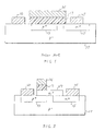
- Fig. 1 schematically shows in vertical section a conventional tunnel transistor; and
- Fig. 2 is a schematic vertical sectional view of a tunnel transistor according to an embodiment of the instant invention.
- Referring to Fig. 1, a conventional tunnel transistor will first be described in order to facilitate an understanding of the present invention. The conventional tunnel transistor is of the type illustrated in the Banerjee et al letter referred to hereinabove.
- Contiguous to a principal surface of a
semiconductor substrate 11, first and seconddegenerate semiconductor layers 13 and 15 are formed in thesubstrate 11. It will be presumed that thesubstrate 11 is made of silicon doped with a p-type impurity to a relatively lower impurity concentration of 1 x 10¹⁵ per cubic centimeter and that the first and the second (degenerate)semiconductor layers 13 and 15 are made also of silicon. In this event, thefirst semiconductor layer 13 is doped with the p-type impurity to a higher (impurity) concentration of 5 x 10¹⁷ per cubic centimeter to serve as a source region. The second semiconductor layer 15 is doped with an n-type impurity to the higher concentration to serve as a drain region. A portion of thesubstrate 11 is left between the first and thesecond semiconductor layers 13 and 15 as a spacer region having a length of 0.5 to 90 µm (microns) between the first and thesecond semiconductor layers 13 and 15. It is possible to make the spacer region have a shorter length of 0.1 µm (micron). - An insulating film 17 of silicon dioxide is formed on the principal surface to a thickness of from 5 to 30 nanometers to cover the
first semiconductor layer 13 and the spacer region and partly the second semiconductor layer 15, thereby providing a gate-drain overlapping region of a length of from 0.5 to 90 µm (microns) along the principal surface and leaving a remaining portion of the second semiconductor layer 15 uncovered. The insulating film 17 serves as a gate oxide film. Around the gate oxide film 17, the principal surface is left exposed as an exposed surface. - A
gate electrode 21 of polysilicon is formed on the gate oxide film 17 to lie over thefirst semiconductor layer 13, the spacer region, and the gate-drain overlapping region. The polysilicon is doped with the n-type impurity to the higher concentration. Source anddrain electrodes substrate 11 at the exposed surface adjacent to thefirst semiconductor layer 13 and with the remaining portion of the second semiconductor layer 15. - In operation, it will first be assumed that the gate and the
source electrodes drain electrode 25 given a positive voltage. Under the circumstances, a combination of the source and the drain regions serve as a p--n+ diode supplied with a reversed bias voltage. As a consequence, no drain current is obtained at thedrain electrode 25. - It will now be assumed that the
gate electrode 21 is supplied with a sufficiently high positive voltage, such as about 10 volts, as a gate voltage. In this event, an inversion layer appears in the spacer region below the gate oxide film 17. The inversion layer will herein be called a spacer inversion layer, in which electrons are induced. - Another inversion layer appears along a surface which the
first semiconductor layer 13 has contiguous to the gate oxide film 17. This inversion layer will be called a surface inversion layer. Doped to a high impurity concentration, the surface inversion layer is subjected to a high electric field, such as 1 MV/cm. This high electric field gives rise to tunnelling electrons which flow from the valence band of thefirst semiconductor layer 13 to the conduction band of the surface inversion layer. - The tunnelling electrons flow as a tunnelling current through the spacer inversion layer towards the second semiconductor layer 15 with electrons supplied from the
source electrode 23 through thesubstrate 11 to the valence band of thefirst semiconductor layer 13. As a result, the drain current flows to put the tunnel transistor in transistor operation. - In the manner described in the foregoing, the transistor operation is achieved with the conventional tunnel transistor by controlling the tunnelling current which flows from the highly doped source region to the surface inversion layer. It is therefore impossible to raise the impurity concentration of the
first semiconductor layer 13 and to give a high carrier density to the surface inversion layer. The carrier density is at most 1 x 10¹⁹ per cubic centimeter. This makes it impossible to get a great tunnelling current. In addition, the tunnel transistor has an equivalent circuit in which a tunnel junction is connected in series with a parasitic metal-oxide-semiconductor field effect transistor. This gives rise to a problem such that a high-speed operation is impossible. - Referring now to Fig. 2, the description will proceed to a tunnel transistor according to a preferred embodiment of this invention. The tunnel transistor comprises similar parts which are designated by like reference numerals and are similarly operable unless otherwise specified in the following.
- In Fig. 2, the tunnel transistor comprises a third
degenerate semiconductor layer 27 formed on the principal surface of thesemiconductor substrate 11 and doped with the n-type impurity to the higher concentration. The third (degenerate)semiconductor layer 27 covers the spacer region and first and second parts of the first and thesecond semiconductor layers 13 and 15 to leave third and fourth parts of the first and thesecond semiconductor layers 13 and 15 uncovered. The third and the fourth parts are remaining portions of the first and thesecond semiconductor layers 13 and 15 other than the first and the second parts, respectively. - The insulating or the gate oxide film 17 is now formed on the
third semiconductor layer 27 over the first part of thefirst semiconductor layer 13. The gate oxide film 17 has a wider forbidden bandwidth than thethird semiconductor layer 27 and than the first and the second semiconductor layers 13 and 15. Thegate electrode 21 is formed on the gate oxide film 17. Thedrain electrode 25 is formed on the fourth part of the second semiconductor layer 15 to form an ohmic junction with the second semiconductor layer 15. - In contrast to the tunnel transistor illustrated with reference to Fig. 1, the tunnel transistor of Fig. 2 has no gate-drain overlapping region. In addition, the
source electrode 23 is formed on the third part of thefirst semiconductor layer 13 to form another ohmic junction with thefirst semiconductor layer 13. Formation of thesource electrode 23 on thefirst semiconductor layer 13 allows the tunnel transistors of Fig. 2 more highly integrated than those illustrated with reference to Fig. 1. - The illustrated tunnel transistor was manufactured as follows. The
semiconductor substrate 11 was made of silicon doped with boron to the relatively lower impurity concentration which is not higher than 1 x 10¹⁵ per cubic centimeter. Thefirst semiconductor layer 13 was formed by boron ion implantation into thesubstrate 11 to a predetermined depth and to the higher concentration in the manner known in the art. Similarly, the second semiconductor layer 15 was formed by arsenic ion implantation to the predetermined depth and to the higher concentration. It is desirable that the length of the spacer region should be sufficient to prevent a tunnelling current from flowing between the first and the second semiconductor layers 13 and 15. The length should therefore be 10 nanometers or more. - The
third semiconductor layer 27 was grown on the principal surface to an initial thickness of 10 nanometers by molecular beam epitaxy (MBE) of silicon doped with arsenic to an impurity concentration of 3 x 10¹⁹ per cubic centimeter. The gate oxide film 17 was formed by thermal surface oxidation of thethird semiconductor layer 27 to a film thickness of 10 nanometers in the known manner. After formation of the gate oxide film 17, thethird semiconductor layer 27 had a layer thickness of 6 nanometers between the gate oxide film 17 and the first part of thefirst semiconductor layer 13. Thethird semiconductor layer 27 is therefore referred to alternatively as a semiconductor film. After thegate electrode 21 was formed of n-type polysilicon, aluminium was evaporated to provide the source and thedrain electrodes - The first and the second semiconductor layers 13 and 15 should have an impurity concentration which allows formation of the ohmic junctions with the source and the
drain electrodes - The predetermined depth should be as thin as possible. In practice, each of the first and the second semiconductor layers 13 and 15 was formed to a depth which was not greater than 100 nanometers. Each of the first and the second parts of the first and the second semiconductor layers 13 and 15 should have a length determined in consideration of an electric current which should be obtained from the:tunnel transistor. In practice, the length should be substantially equal to the length of the spacer region in order to achieve a high degree of integration. Each of the first and the second semiconductor layers 13 and 15 should have a width which is similar to that used in an ordinary field effect transistor.
- In operation, it will first be assumed as before that the gate and the
source electrodes drain electrode 25 is given a positive voltage of from 0.1 to 1.0 volt. No current flows through the spacer region in the manner described in conjunction with Fig. 1. Thethird semiconductor layer 27, however, forms a p+-n+ tunnel junction relative to thefirst semiconductor layer 13 and an n+-n+ ohmic junction with the second semiconductor layer 15. As a consequence, a great drain current flows between the source and thedrain electrodes - It will now be assumed that the
gate electrode 21 is given a negative gate voltage of an absolute value of from 0.1 to 0.3 volt. In such an event, electrons are driven away from a surface portion which thethird semiconductor layer 27 has in contact with the gate oxide film 17. Therefore, the tunnel transistor is of a depletion type wherein a depletion layer grows from the surface portion. - When the negative gate voltage is increased in the absolute value to 0.5 volt, the depletion layer merges into another depletion layer which extends from the tunnel junction. This reduces an overlap of the valence band of the
first semiconductor layer 13 with the conduction band of thethird semiconductor layer 27 to reduce the tunnelling current which flows from thefirst semiconductor layer 13 to thethird semiconductor layer 27. When the negative gate voltage is very high in the absolute value, such as 1 volt, the tunnelling current no more flows. The drain current is therefore rendered zero. - It should be noted in connection with the conventional tunnel transistor that the gate voltage controls an electric potential at an interface between the
first semiconductor layer 13 and the gate oxide film 17. In contrast, the gate voltage does not control the electric potential at the tunnel junction in the tunnel transistor being illustrated. It is therefore possible to give a theoretically unlimitedly high carrier density to thefirst semiconductor layer 13. The high carrier density is, for example, 5 x 10¹⁹ per cubic centimeter. The tunnelling current grows exponentially with the carrier density. The tunnelling current is therefore about three digits greater than that achieved with the conventional tunnel transister. - Furthermore, the
third semiconductor layer 27 spans the first and the second semiconductor layers 13 and 15. The great tunnelling current can therefore flow between the first and the second semiconductor layers 13 and 15 with no hindrance. - In addition, the illustrated tunnel transistor comprises no parastic metal-oxide-semiconductor field effect transistor. The tunnel transistor is therefore operable at a high speed.
- Further in addition, it is possible to put the tunnel transistor into operation with the
drain electrode 25 given a negative voltage relative to thesource electrode 23 provided that the negative voltage is below a build-up voltage of the tunnel transistor. In such an event, control is carried out on a differential negative resistance which is characteristic to a tunnel or Esaki diode. The tunnel transistor is consequently operable as a multifunctional element. - In Fig. 2, the tunnel transistor may be of an enhancement type rather than the depletion type in the manner described in the foregoing. When the tunnel transistor is of the enhancement type, the drain current does not flow while the
gate electrode 21 is grounded. The drain current begins to flow when the gate voltage is supplied. It should, however, be noted in this event that thethird semiconductor layer 27 should be given a thinner layer thickness between the gate oxide film 17 and the first part of thefirst semiconductor layer 13 than that used in the tunnel transistor of the depletion type. The layer thickness should be such that no carrier is present in thethird semiconductor layer 27 put in thermal equilibrium. The thinner layer thickness may be 4 nanometers when the impurity concentration is 3 x 10¹⁹ per cubic centimeter in thethird semiconductor layer 27. - While this invention has thus far been described in specific conjunction with a single embodiment thereof and in connection with a few manners of putting the tunnel transistor into operation, it will now be readily possible for one skilled in the art to put this invention into effect in various other manners: the semiconductor material can be any one of germanium, gallium arsenide, indium phosphide, gallium antimonide, indium arsenide, InGaAs, and other known semicunductor materials. The first through the third semiconductor layers 13, 15, and 27 may not form homojunctions but may form heterojunctions. The p-type impurity can be any one of known impurities other than boron. Likewise, the n-type impurity can be any one of known impurities other than arsenic.
- The insulating film 17 can be made of any one of other insulating materials provided that the insulating material has a wider forbidden bandwidth than the semiconductor material of the
third semiconductor layer 27 and than the semiconductor material or materials of the first and the second semiconductor layers 13 and 15. For example, the insulating material may be silicon nitride (Si3N4) or aluminium nitride (AlN). The "insulating" material can be a semiconductor material having a wider forbidden bandwidth than the semiconductor material of thethird semiconductor layer 27 and than the semiconductor material or materials of the first and the second semiconductor layers 13 and 15. For example, the "insulating" material may be gallium phosphide and AlGaAs when the first through the third semiconductor layers 13, 15, and 27 are made of silicon and of gallium arsenide, respectively. As a consequence, the insulating or the gate oxide film 17 is alternatively referred to herein as a gate isolating or spacing film.
Claims (15)
- A tunnel transistor including a semiconductor substrate (11) having a principal surface and doped with an impurity of a first conductivity type; degenerate first (13) and second (15) semiconductor layers located in said semiconductor substrate (11) contiguous to said principal surface, spaced one from the other by a spacer region of said semiconductor substrate (11) and doped with an impurity of said first conductivity type and with an impurity of a second conductivity type, respectively, each semiconductor layer being doped to a higher concentration than that to which the substrate is doped, said tunnel transistor comprising:a degenerate third semiconductor layer (27) formed on said principal surface, doped with an impurity of said second conductivity type, covering said spacer region and first and second parts of said first and said second semiconductor layers (13,15) and leaving third and fourth parts of said first and said second semiconductor layers (13,15) uncovered, said third semiconductor layer (27) forming a tunnel junction with said first part of said first semiconductor layer (13);a gate isolating film (17) formed on said third semiconductor layer over said first part of the first semiconductor layer (13) and having a wider forbidden bandwidth than said third semiconductor layer (27);a gate electrode (21) on said gate isolating film; anda pair of electrodes (23,25) located on said third and said fourth parts of the first and the second semiconductor layers (13,15) and forming ohmic contacts therewith.
- A tunnel transistor as claimed in Claim 1, wherein said gate isolating film (17) is made of an insulating material.
- A tunnel transistor as claimed in Claim 2, wherein said third semiconductor layer (27) is made of a material selected from silicon, germanium, gallium arsenide, indium phosphide, gallium antimonide, indium arsenide, and InGaAs, and said insulating material is selected from silicon dioxide, silicon nitride, and aluminium nitride.
- A tunnel transistor as claimed in Claim 2, wherein said third semiconductor layer (27) is doped to a concentration which is at least as high as the doping concentrations of said first and said second semiconductor layers (13,15).
- A tunnel transistor as claimed in Claim 4, wherein said third semiconductor layer (27) forms a tunnel homojunction with said first part of the first semiconductor layer (13) and a homojunction with said second part of the second semiconductor layer (15).
- A tunnel transistor as claimed in Claim 4, wherein said third semiconductor layer (27) forms a tunnel homojunction with said first part of the first semiconductor layer (13) and a heterojunction with said second part of the second semiconductor layer (15).
- A tunnel transistor as claimed in Claim 4, wherein said third semiconductor layer (27) forms a tunnel heterojunction with said first part of the first semiconductor layer (13) and a homojunction with said second part of the second semiconductor layer (15).
- A tunnel transistor as claimed in Claim 4, wherein said third semiconductor layer (27) forms a tunnel heterojunction with said first part of the first semiconductor layer (13) and a heterojunction with said second part of the second semiconductor layer (15).
- A tunnel transistor as claimed in Claim 1, wherein said gate isolating film is made of a semiconductor material having a wider forbidden bandwidth than the semiconductor material of the first semiconductor layer (13).
- A tunnel transistor as claimed in Claim 9, wherein said third semiconductor layer (27) is made of a material selected from silicon and gallium arsenide, and wherein said second semiconductor material is gallium phosphide if said third semiconductor layer (27) is made of silicon and AlGaAs if said third semiconductor layer (27) is made of gallium arsenide.
- A tunnel transistor as claimed in Claim 9, wherein said third semiconductor layer (27) is doped to a concentration which is at least as high as the doping concentrations of said first and said second semiconductor layers (13,15).
- A tunnel transistor as claimed in Claim 11, wherein said third semiconductor layer (27) forms a tunnel homojunction with said first part of the first semiconductor layer (13) and a homojunction with said second part of the second semiconductor layer (15).
- A tunnel transistor as claimed in Claim 11, wherein said third semiconductor layer (27) forms a tunnel homojunction with said first part of the first semiconductor layer (13) and a heterojunction with said second part of the second semiconductor layer (15).
- A tunnel transistor as claimed in Claim 11, wherein said third semiconductor layer (27) forms a tunnel heterojunction with said first part of the first semiconductor layer (13) and a homojunction with said second part of the second semiconductor layer (15).
- A tunnel transistor as claimed in Claim 11, wherein said third semiconductor layer (27) forms a tunnel heterojunction with said first part of the first semiconductor layer (13) and a heterojunction with said second part of the second semiconductor layer (15).
Applications Claiming Priority (2)
| Application Number | Priority Date | Filing Date | Title |
|---|---|---|---|
| JP265749/91 | 1991-10-15 | ||
| JP3265749A JP2773487B2 (en) | 1991-10-15 | 1991-10-15 | Tunnel transistor |
Publications (3)
| Publication Number | Publication Date |
|---|---|
| EP0538036A2 EP0538036A2 (en) | 1993-04-21 |
| EP0538036A3 EP0538036A3 (en) | 1995-03-22 |
| EP0538036B1 true EP0538036B1 (en) | 1997-04-16 |
Family
ID=17421473
Family Applications (1)
| Application Number | Title | Priority Date | Filing Date |
|---|---|---|---|
| EP92309417A Expired - Lifetime EP0538036B1 (en) | 1991-10-15 | 1992-10-15 | Tunnel transistor |
Country Status (4)
| Country | Link |
|---|---|
| US (1) | US5589696A (en) |
| EP (1) | EP0538036B1 (en) |
| JP (1) | JP2773487B2 (en) |
| DE (1) | DE69219057T2 (en) |
Families Citing this family (39)
| Publication number | Priority date | Publication date | Assignee | Title |
|---|---|---|---|---|
| DE69202554T2 (en) * | 1991-12-25 | 1995-10-19 | Nec Corp | Tunnel transistor and its manufacturing process. |
| US6693317B2 (en) * | 2001-07-13 | 2004-02-17 | Taiwan Semiconductor Manufacturing Company | Optical sensor by using tunneling diode |
| WO2004001801A2 (en) * | 2002-06-19 | 2003-12-31 | The Board Of Trustees Of The Leland Stanford Junior University | Insulated-gate semiconductor device and approach involving junction-induced intermediate region |
| CN1762047A (en) | 2003-03-20 | 2006-04-19 | 松下电器产业株式会社 | Semiconductor device and method for fabricating the same |
| US8324660B2 (en) | 2005-05-17 | 2012-12-04 | Taiwan Semiconductor Manufacturing Company, Ltd. | Lattice-mismatched semiconductor structures with reduced dislocation defect densities and related methods for device fabrication |
| US9153645B2 (en) | 2005-05-17 | 2015-10-06 | Taiwan Semiconductor Manufacturing Company, Ltd. | Lattice-mismatched semiconductor structures with reduced dislocation defect densities and related methods for device fabrication |
| CN101268547B (en) | 2005-07-26 | 2014-07-09 | 琥珀波系统公司 | Solutions for integrated circuit integration of alternative active area materials |
| US7638842B2 (en) | 2005-09-07 | 2009-12-29 | Amberwave Systems Corporation | Lattice-mismatched semiconductor structures on insulators |
| US8441000B2 (en) * | 2006-02-01 | 2013-05-14 | International Business Machines Corporation | Heterojunction tunneling field effect transistors, and methods for fabricating the same |
| US7777250B2 (en) | 2006-03-24 | 2010-08-17 | Taiwan Semiconductor Manufacturing Company, Ltd. | Lattice-mismatched semiconductor structures and related methods for device fabrication |
| EP2062290B1 (en) | 2006-09-07 | 2019-08-28 | Taiwan Semiconductor Manufacturing Company, Ltd. | Defect reduction using aspect ratio trapping |
| US7875958B2 (en) | 2006-09-27 | 2011-01-25 | Taiwan Semiconductor Manufacturing Company, Ltd. | Quantum tunneling devices and circuits with lattice-mismatched semiconductor structures |
| WO2008039495A1 (en) | 2006-09-27 | 2008-04-03 | Amberwave Systems Corporation | Tri-gate field-effect transistors formed by aspect ratio trapping |
| US8502263B2 (en) | 2006-10-19 | 2013-08-06 | Taiwan Semiconductor Manufacturing Company, Ltd. | Light-emitter-based devices with lattice-mismatched semiconductor structures |
| JP2008252086A (en) * | 2007-03-12 | 2008-10-16 | Interuniv Micro Electronica Centrum Vzw | Tunnel field-effect transistor with gated tunnel barrier |
| US8304805B2 (en) | 2009-01-09 | 2012-11-06 | Taiwan Semiconductor Manufacturing Company, Ltd. | Semiconductor diodes fabricated by aspect ratio trapping with coalesced films |
| WO2008124154A2 (en) | 2007-04-09 | 2008-10-16 | Amberwave Systems Corporation | Photovoltaics on silicon |
| US8237151B2 (en) | 2009-01-09 | 2012-08-07 | Taiwan Semiconductor Manufacturing Company, Ltd. | Diode-based devices and methods for making the same |
| US7825328B2 (en) | 2007-04-09 | 2010-11-02 | Taiwan Semiconductor Manufacturing Company, Ltd. | Nitride-based multi-junction solar cell modules and methods for making the same |
| US8329541B2 (en) | 2007-06-15 | 2012-12-11 | Taiwan Semiconductor Manufacturing Company, Ltd. | InP-based transistor fabrication |
| US8344242B2 (en) | 2007-09-07 | 2013-01-01 | Taiwan Semiconductor Manufacturing Company, Ltd. | Multi-junction solar cells |
| US8183667B2 (en) | 2008-06-03 | 2012-05-22 | Taiwan Semiconductor Manufacturing Co., Ltd. | Epitaxial growth of crystalline material |
| US8274097B2 (en) | 2008-07-01 | 2012-09-25 | Taiwan Semiconductor Manufacturing Company, Ltd. | Reduction of edge effects from aspect ratio trapping |
| US8981427B2 (en) | 2008-07-15 | 2015-03-17 | Taiwan Semiconductor Manufacturing Company, Ltd. | Polishing of small composite semiconductor materials |
| US20100072515A1 (en) | 2008-09-19 | 2010-03-25 | Amberwave Systems Corporation | Fabrication and structures of crystalline material |
| WO2010033813A2 (en) | 2008-09-19 | 2010-03-25 | Amberwave System Corporation | Formation of devices by epitaxial layer overgrowth |
| US8253211B2 (en) | 2008-09-24 | 2012-08-28 | Taiwan Semiconductor Manufacturing Company, Ltd. | Semiconductor sensor structures with reduced dislocation defect densities |
| SG171987A1 (en) | 2009-04-02 | 2011-07-28 | Taiwan Semiconductor Mfg | Devices formed from a non-polar plane of a crystalline material and method of making the same |
| JP5910965B2 (en) * | 2012-03-07 | 2016-04-27 | 国立研究開発法人産業技術総合研究所 | Tunnel field effect transistor manufacturing method and tunnel field effect transistor |
| EP2674978B1 (en) * | 2012-06-15 | 2020-07-29 | IMEC vzw | Tunnel field effect transistor device and method for making the device |
| JP2014053435A (en) | 2012-09-06 | 2014-03-20 | Toshiba Corp | Semiconductor device |
| EP2808897B1 (en) | 2013-05-30 | 2021-06-30 | IMEC vzw | Tunnel field effect transistor and method for making thereof |
| US8975123B2 (en) | 2013-07-09 | 2015-03-10 | International Business Machines Corporation | Tunnel field-effect transistors with a gate-swing broken-gap heterostructure |
| JP6331375B2 (en) * | 2013-12-17 | 2018-05-30 | 富士通株式会社 | Field effect semiconductor device |
| JP6175411B2 (en) * | 2014-06-16 | 2017-08-02 | 東芝メモリ株式会社 | Semiconductor device |
| WO2016168994A1 (en) * | 2015-04-22 | 2016-10-27 | 华为技术有限公司 | Tunnelling transistor and tunnelling transistor manufacturing method |
| CN109065615B (en) * | 2018-06-12 | 2021-05-07 | 西安电子科技大学 | Novel planar InAs/Si heterogeneous tunneling field effect transistor and preparation method thereof |
| CN110459541B (en) * | 2019-06-27 | 2022-05-13 | 西安电子科技大学 | Planar complementary type tunneling field effect transistor inverter |
| CN111640791A (en) * | 2020-04-26 | 2020-09-08 | 西安电子科技大学 | Quantum well tunneling field effect transistor based on InAs/GaSb heterojunction and preparation method thereof |
Family Cites Families (9)
| Publication number | Priority date | Publication date | Assignee | Title |
|---|---|---|---|---|
| US3390352A (en) * | 1961-11-06 | 1968-06-25 | Itt | Tunnel-effect semiconductor, used as an oscillator or amplifier, forms part of surface of waveguide or chamber |
| JPH0673375B2 (en) * | 1984-03-19 | 1994-09-14 | 富士通株式会社 | Method for manufacturing semiconductor device |
| EP0181191B1 (en) * | 1984-11-05 | 1996-02-28 | Hitachi, Ltd. | Superconducting device |
| JPS63250855A (en) * | 1987-04-08 | 1988-10-18 | Hitachi Ltd | Bipolar transistor |
| US4969019A (en) * | 1987-08-27 | 1990-11-06 | Texas Instruments Incorporated | Three-terminal tunnel device |
| JPH02268429A (en) * | 1989-04-11 | 1990-11-02 | Tokyo Electron Ltd | Plasma etching apparatus |
| US5105247A (en) * | 1990-08-03 | 1992-04-14 | Cavanaugh Marion E | Quantum field effect device with source extension region formed under a gate and between the source and drain regions |
| EP0480814B1 (en) * | 1990-10-08 | 1996-04-24 | Sumitomo Electric Industries, Ltd. | Superconducting device having an extremely thin superconducting channel formed of oxide superconductor material and method for manufacturing the same |
| JPH05235057A (en) * | 1992-02-19 | 1993-09-10 | Sanyo Electric Co Ltd | Semiconductor device |
-
1991
- 1991-10-15 JP JP3265749A patent/JP2773487B2/en not_active Expired - Lifetime
-
1992
- 1992-10-14 US US07/960,863 patent/US5589696A/en not_active Expired - Fee Related
- 1992-10-15 DE DE69219057T patent/DE69219057T2/en not_active Expired - Fee Related
- 1992-10-15 EP EP92309417A patent/EP0538036B1/en not_active Expired - Lifetime
Also Published As
| Publication number | Publication date |
|---|---|
| EP0538036A2 (en) | 1993-04-21 |
| DE69219057D1 (en) | 1997-05-22 |
| EP0538036A3 (en) | 1995-03-22 |
| JPH05110086A (en) | 1993-04-30 |
| JP2773487B2 (en) | 1998-07-09 |
| DE69219057T2 (en) | 1998-02-26 |
| US5589696A (en) | 1996-12-31 |
Similar Documents
| Publication | Publication Date | Title |
|---|---|---|
| EP0538036B1 (en) | Tunnel transistor | |
| US5155571A (en) | Complementary field effect transistors having strained superlattice structure | |
| US5179037A (en) | Integration of lateral and vertical quantum well transistors in the same epitaxial stack | |
| US4556895A (en) | Field-effect transistor having a channel region of a Group III-V compound semiconductor and a Group IV semiconductor | |
| JP2500063B2 (en) | Field effect transistor | |
| EP0256360B1 (en) | Gated tunnel diode | |
| EP0184827A2 (en) | A high speed and high power transistor | |
| US4317127A (en) | Static induction transistor and integrated circuit utilizing same | |
| JP2929899B2 (en) | Field-effect transistor with nonlinear transfer characteristics | |
| EP0306258B1 (en) | Transistor | |
| JPH0783107B2 (en) | Field effect transistor | |
| JPH0624208B2 (en) | Semiconductor device | |
| EP0566591B1 (en) | Semiconductor device | |
| US5351128A (en) | Semiconductor device having reduced contact resistance between a channel or base layer and a contact layer | |
| US4903091A (en) | Heterojunction transistor having bipolar characteristics | |
| US5552330A (en) | Resonant tunneling fet and methods of fabrication | |
| US5489785A (en) | Band-to-band resonant tunneling transistor | |
| EP0092645B1 (en) | Transistor and circuit including a transistor | |
| JP2800675B2 (en) | Tunnel transistor | |
| JP2643890B2 (en) | Tunnel transistor | |
| JPH07193232A (en) | Conductivity modulation type transistor | |
| JPS639386B2 (en) | ||
| JP3054216B2 (en) | Semiconductor device | |
| JPH0620142B2 (en) | Semiconductor device | |
| JP2671553B2 (en) | Field effect semiconductor device |
Legal Events
| Date | Code | Title | Description |
|---|---|---|---|
| PUAI | Public reference made under article 153(3) epc to a published international application that has entered the european phase |
Free format text: ORIGINAL CODE: 0009012 |
|
| AK | Designated contracting states |
Kind code of ref document: A2 Designated state(s): DE FR GB |
|
| PUAL | Search report despatched |
Free format text: ORIGINAL CODE: 0009013 |
|
| AK | Designated contracting states |
Kind code of ref document: A3 Designated state(s): DE FR GB |
|
| RHK1 | Main classification (correction) |
Ipc: H01L 29/72 |
|
| 17P | Request for examination filed |
Effective date: 19950304 |
|
| GRAG | Despatch of communication of intention to grant |
Free format text: ORIGINAL CODE: EPIDOS AGRA |
|
| 17Q | First examination report despatched |
Effective date: 19960531 |
|
| GRAH | Despatch of communication of intention to grant a patent |
Free format text: ORIGINAL CODE: EPIDOS IGRA |
|
| GRAH | Despatch of communication of intention to grant a patent |
Free format text: ORIGINAL CODE: EPIDOS IGRA |
|
| GRAA | (expected) grant |
Free format text: ORIGINAL CODE: 0009210 |
|
| AK | Designated contracting states |
Kind code of ref document: B1 Designated state(s): DE FR GB |
|
| REF | Corresponds to: |
Ref document number: 69219057 Country of ref document: DE Date of ref document: 19970522 |
|
| ET | Fr: translation filed | ||
| PLBE | No opposition filed within time limit |
Free format text: ORIGINAL CODE: 0009261 |
|
| STAA | Information on the status of an ep patent application or granted ep patent |
Free format text: STATUS: NO OPPOSITION FILED WITHIN TIME LIMIT |
|
| 26N | No opposition filed | ||
| REG | Reference to a national code |
Ref country code: GB Ref legal event code: IF02 |
|
| PGFP | Annual fee paid to national office [announced via postgrant information from national office to epo] |
Ref country code: FR Payment date: 20021008 Year of fee payment: 11 |
|
| PGFP | Annual fee paid to national office [announced via postgrant information from national office to epo] |
Ref country code: GB Payment date: 20021009 Year of fee payment: 11 |
|
| PGFP | Annual fee paid to national office [announced via postgrant information from national office to epo] |
Ref country code: DE Payment date: 20021017 Year of fee payment: 11 |
|
| PG25 | Lapsed in a contracting state [announced via postgrant information from national office to epo] |
Ref country code: GB Free format text: LAPSE BECAUSE OF NON-PAYMENT OF DUE FEES Effective date: 20031015 |
|
| PG25 | Lapsed in a contracting state [announced via postgrant information from national office to epo] |
Ref country code: DE Free format text: LAPSE BECAUSE OF NON-PAYMENT OF DUE FEES Effective date: 20040501 |
|
| GBPC | Gb: european patent ceased through non-payment of renewal fee |
Effective date: 20031015 |
|
| PG25 | Lapsed in a contracting state [announced via postgrant information from national office to epo] |
Ref country code: FR Free format text: LAPSE BECAUSE OF NON-PAYMENT OF DUE FEES Effective date: 20040630 |
|
| REG | Reference to a national code |
Ref country code: FR Ref legal event code: ST |