EP0533164B1 - Ball-Bondverfahren und Vorrichtung zur Durchführung desselben - Google Patents
Ball-Bondverfahren und Vorrichtung zur Durchführung desselben Download PDFInfo
- Publication number
- EP0533164B1 EP0533164B1 EP92115937A EP92115937A EP0533164B1 EP 0533164 B1 EP0533164 B1 EP 0533164B1 EP 92115937 A EP92115937 A EP 92115937A EP 92115937 A EP92115937 A EP 92115937A EP 0533164 B1 EP0533164 B1 EP 0533164B1
- Authority
- EP
- European Patent Office
- Prior art keywords
- bonding
- wire
- free
- singeing
- ball
- Prior art date
- Legal status (The legal status is an assumption and is not a legal conclusion. Google has not performed a legal analysis and makes no representation as to the accuracy of the status listed.)
- Expired - Lifetime
Links
Images
Classifications
-
- H—ELECTRICITY
- H01—ELECTRIC ELEMENTS
- H01L—SEMICONDUCTOR DEVICES NOT COVERED BY CLASS H10
- H01L24/00—Arrangements for connecting or disconnecting semiconductor or solid-state bodies; Methods or apparatus related thereto
- H01L24/80—Methods for connecting semiconductor or other solid state bodies using means for bonding being attached to, or being formed on, the surface to be connected
- H01L24/85—Methods for connecting semiconductor or other solid state bodies using means for bonding being attached to, or being formed on, the surface to be connected using a wire connector
-
- B—PERFORMING OPERATIONS; TRANSPORTING
- B23—MACHINE TOOLS; METAL-WORKING NOT OTHERWISE PROVIDED FOR
- B23K—SOLDERING OR UNSOLDERING; WELDING; CLADDING OR PLATING BY SOLDERING OR WELDING; CUTTING BY APPLYING HEAT LOCALLY, e.g. FLAME CUTTING; WORKING BY LASER BEAM
- B23K20/00—Non-electric welding by applying impact or other pressure, with or without the application of heat, e.g. cladding or plating
- B23K20/002—Non-electric welding by applying impact or other pressure, with or without the application of heat, e.g. cladding or plating specially adapted for particular articles or work
- B23K20/004—Wire welding
- B23K20/005—Capillary welding
- B23K20/007—Ball bonding
-
- H—ELECTRICITY
- H01—ELECTRIC ELEMENTS
- H01L—SEMICONDUCTOR DEVICES NOT COVERED BY CLASS H10
- H01L21/00—Processes or apparatus adapted for the manufacture or treatment of semiconductor or solid state devices or of parts thereof
- H01L21/02—Manufacture or treatment of semiconductor devices or of parts thereof
- H01L21/04—Manufacture or treatment of semiconductor devices or of parts thereof the devices having at least one potential-jump barrier or surface barrier, e.g. PN junction, depletion layer or carrier concentration layer
- H01L21/50—Assembly of semiconductor devices using processes or apparatus not provided for in a single one of the subgroups H01L21/06 - H01L21/326, e.g. sealing of a cap to a base of a container
- H01L21/60—Attaching or detaching leads or other conductive members, to be used for carrying current to or from the device in operation
-
- H—ELECTRICITY
- H01—ELECTRIC ELEMENTS
- H01L—SEMICONDUCTOR DEVICES NOT COVERED BY CLASS H10
- H01L24/00—Arrangements for connecting or disconnecting semiconductor or solid-state bodies; Methods or apparatus related thereto
- H01L24/74—Apparatus for manufacturing arrangements for connecting or disconnecting semiconductor or solid-state bodies
- H01L24/78—Apparatus for connecting with wire connectors
-
- H—ELECTRICITY
- H01—ELECTRIC ELEMENTS
- H01L—SEMICONDUCTOR DEVICES NOT COVERED BY CLASS H10
- H01L2224/00—Indexing scheme for arrangements for connecting or disconnecting semiconductor or solid-state bodies and methods related thereto as covered by H01L24/00
- H01L2224/01—Means for bonding being attached to, or being formed on, the surface to be connected, e.g. chip-to-package, die-attach, "first-level" interconnects; Manufacturing methods related thereto
- H01L2224/42—Wire connectors; Manufacturing methods related thereto
- H01L2224/44—Structure, shape, material or disposition of the wire connectors prior to the connecting process
- H01L2224/45—Structure, shape, material or disposition of the wire connectors prior to the connecting process of an individual wire connector
- H01L2224/45001—Core members of the connector
- H01L2224/45099—Material
- H01L2224/451—Material with a principal constituent of the material being a metal or a metalloid, e.g. boron (B), silicon (Si), germanium (Ge), arsenic (As), antimony (Sb), tellurium (Te) and polonium (Po), and alloys thereof
- H01L2224/45138—Material with a principal constituent of the material being a metal or a metalloid, e.g. boron (B), silicon (Si), germanium (Ge), arsenic (As), antimony (Sb), tellurium (Te) and polonium (Po), and alloys thereof the principal constituent melting at a temperature of greater than or equal to 950°C and less than 1550°C
- H01L2224/45144—Gold (Au) as principal constituent
-
- H—ELECTRICITY
- H01—ELECTRIC ELEMENTS
- H01L—SEMICONDUCTOR DEVICES NOT COVERED BY CLASS H10
- H01L2224/00—Indexing scheme for arrangements for connecting or disconnecting semiconductor or solid-state bodies and methods related thereto as covered by H01L24/00
- H01L2224/01—Means for bonding being attached to, or being formed on, the surface to be connected, e.g. chip-to-package, die-attach, "first-level" interconnects; Manufacturing methods related thereto
- H01L2224/42—Wire connectors; Manufacturing methods related thereto
- H01L2224/47—Structure, shape, material or disposition of the wire connectors after the connecting process
- H01L2224/48—Structure, shape, material or disposition of the wire connectors after the connecting process of an individual wire connector
- H01L2224/4805—Shape
- H01L2224/4809—Loop shape
- H01L2224/48091—Arched
-
- H—ELECTRICITY
- H01—ELECTRIC ELEMENTS
- H01L—SEMICONDUCTOR DEVICES NOT COVERED BY CLASS H10
- H01L2224/00—Indexing scheme for arrangements for connecting or disconnecting semiconductor or solid-state bodies and methods related thereto as covered by H01L24/00
- H01L2224/01—Means for bonding being attached to, or being formed on, the surface to be connected, e.g. chip-to-package, die-attach, "first-level" interconnects; Manufacturing methods related thereto
- H01L2224/42—Wire connectors; Manufacturing methods related thereto
- H01L2224/47—Structure, shape, material or disposition of the wire connectors after the connecting process
- H01L2224/48—Structure, shape, material or disposition of the wire connectors after the connecting process of an individual wire connector
- H01L2224/481—Disposition
- H01L2224/48151—Connecting between a semiconductor or solid-state body and an item not being a semiconductor or solid-state body, e.g. chip-to-substrate, chip-to-passive
- H01L2224/48221—Connecting between a semiconductor or solid-state body and an item not being a semiconductor or solid-state body, e.g. chip-to-substrate, chip-to-passive the body and the item being stacked
- H01L2224/48225—Connecting between a semiconductor or solid-state body and an item not being a semiconductor or solid-state body, e.g. chip-to-substrate, chip-to-passive the body and the item being stacked the item being non-metallic, e.g. insulating substrate with or without metallisation
- H01L2224/48227—Connecting between a semiconductor or solid-state body and an item not being a semiconductor or solid-state body, e.g. chip-to-substrate, chip-to-passive the body and the item being stacked the item being non-metallic, e.g. insulating substrate with or without metallisation connecting the wire to a bond pad of the item
-
- H—ELECTRICITY
- H01—ELECTRIC ELEMENTS
- H01L—SEMICONDUCTOR DEVICES NOT COVERED BY CLASS H10
- H01L2224/00—Indexing scheme for arrangements for connecting or disconnecting semiconductor or solid-state bodies and methods related thereto as covered by H01L24/00
- H01L2224/01—Means for bonding being attached to, or being formed on, the surface to be connected, e.g. chip-to-package, die-attach, "first-level" interconnects; Manufacturing methods related thereto
- H01L2224/42—Wire connectors; Manufacturing methods related thereto
- H01L2224/47—Structure, shape, material or disposition of the wire connectors after the connecting process
- H01L2224/48—Structure, shape, material or disposition of the wire connectors after the connecting process of an individual wire connector
- H01L2224/481—Disposition
- H01L2224/48151—Connecting between a semiconductor or solid-state body and an item not being a semiconductor or solid-state body, e.g. chip-to-substrate, chip-to-passive
- H01L2224/48221—Connecting between a semiconductor or solid-state body and an item not being a semiconductor or solid-state body, e.g. chip-to-substrate, chip-to-passive the body and the item being stacked
- H01L2224/48245—Connecting between a semiconductor or solid-state body and an item not being a semiconductor or solid-state body, e.g. chip-to-substrate, chip-to-passive the body and the item being stacked the item being metallic
- H01L2224/48247—Connecting between a semiconductor or solid-state body and an item not being a semiconductor or solid-state body, e.g. chip-to-substrate, chip-to-passive the body and the item being stacked the item being metallic connecting the wire to a bond pad of the item
-
- H—ELECTRICITY
- H01—ELECTRIC ELEMENTS
- H01L—SEMICONDUCTOR DEVICES NOT COVERED BY CLASS H10
- H01L2224/00—Indexing scheme for arrangements for connecting or disconnecting semiconductor or solid-state bodies and methods related thereto as covered by H01L24/00
- H01L2224/01—Means for bonding being attached to, or being formed on, the surface to be connected, e.g. chip-to-package, die-attach, "first-level" interconnects; Manufacturing methods related thereto
- H01L2224/42—Wire connectors; Manufacturing methods related thereto
- H01L2224/47—Structure, shape, material or disposition of the wire connectors after the connecting process
- H01L2224/48—Structure, shape, material or disposition of the wire connectors after the connecting process of an individual wire connector
- H01L2224/484—Connecting portions
- H01L2224/48463—Connecting portions the connecting portion on the bonding area of the semiconductor or solid-state body being a ball bond
- H01L2224/48464—Connecting portions the connecting portion on the bonding area of the semiconductor or solid-state body being a ball bond the other connecting portion not on the bonding area also being a ball bond, i.e. ball-to-ball
-
- H—ELECTRICITY
- H01—ELECTRIC ELEMENTS
- H01L—SEMICONDUCTOR DEVICES NOT COVERED BY CLASS H10
- H01L2224/00—Indexing scheme for arrangements for connecting or disconnecting semiconductor or solid-state bodies and methods related thereto as covered by H01L24/00
- H01L2224/01—Means for bonding being attached to, or being formed on, the surface to be connected, e.g. chip-to-package, die-attach, "first-level" interconnects; Manufacturing methods related thereto
- H01L2224/42—Wire connectors; Manufacturing methods related thereto
- H01L2224/47—Structure, shape, material or disposition of the wire connectors after the connecting process
- H01L2224/48—Structure, shape, material or disposition of the wire connectors after the connecting process of an individual wire connector
- H01L2224/484—Connecting portions
- H01L2224/48463—Connecting portions the connecting portion on the bonding area of the semiconductor or solid-state body being a ball bond
- H01L2224/48465—Connecting portions the connecting portion on the bonding area of the semiconductor or solid-state body being a ball bond the other connecting portion not on the bonding area being a wedge bond, i.e. ball-to-wedge, regular stitch
-
- H—ELECTRICITY
- H01—ELECTRIC ELEMENTS
- H01L—SEMICONDUCTOR DEVICES NOT COVERED BY CLASS H10
- H01L2224/00—Indexing scheme for arrangements for connecting or disconnecting semiconductor or solid-state bodies and methods related thereto as covered by H01L24/00
- H01L2224/74—Apparatus for manufacturing arrangements for connecting or disconnecting semiconductor or solid-state bodies and for methods related thereto
- H01L2224/78—Apparatus for connecting with wire connectors
- H01L2224/7825—Means for applying energy, e.g. heating means
- H01L2224/783—Means for applying energy, e.g. heating means by means of pressure
- H01L2224/78301—Capillary
-
- H—ELECTRICITY
- H01—ELECTRIC ELEMENTS
- H01L—SEMICONDUCTOR DEVICES NOT COVERED BY CLASS H10
- H01L2224/00—Indexing scheme for arrangements for connecting or disconnecting semiconductor or solid-state bodies and methods related thereto as covered by H01L24/00
- H01L2224/80—Methods for connecting semiconductor or other solid state bodies using means for bonding being attached to, or being formed on, the surface to be connected
- H01L2224/85—Methods for connecting semiconductor or other solid state bodies using means for bonding being attached to, or being formed on, the surface to be connected using a wire connector
- H01L2224/85009—Pre-treatment of the connector or the bonding area
- H01L2224/8503—Reshaping, e.g. forming the ball or the wedge of the wire connector
- H01L2224/85035—Reshaping, e.g. forming the ball or the wedge of the wire connector by heating means, e.g. "free-air-ball"
- H01L2224/85045—Reshaping, e.g. forming the ball or the wedge of the wire connector by heating means, e.g. "free-air-ball" using a corona discharge, e.g. electronic flame off [EFO]
-
- H—ELECTRICITY
- H01—ELECTRIC ELEMENTS
- H01L—SEMICONDUCTOR DEVICES NOT COVERED BY CLASS H10
- H01L2224/00—Indexing scheme for arrangements for connecting or disconnecting semiconductor or solid-state bodies and methods related thereto as covered by H01L24/00
- H01L2224/80—Methods for connecting semiconductor or other solid state bodies using means for bonding being attached to, or being formed on, the surface to be connected
- H01L2224/85—Methods for connecting semiconductor or other solid state bodies using means for bonding being attached to, or being formed on, the surface to be connected using a wire connector
- H01L2224/851—Methods for connecting semiconductor or other solid state bodies using means for bonding being attached to, or being formed on, the surface to be connected using a wire connector the connector being supplied to the parts to be connected in the bonding apparatus
-
- H—ELECTRICITY
- H01—ELECTRIC ELEMENTS
- H01L—SEMICONDUCTOR DEVICES NOT COVERED BY CLASS H10
- H01L2224/00—Indexing scheme for arrangements for connecting or disconnecting semiconductor or solid-state bodies and methods related thereto as covered by H01L24/00
- H01L2224/80—Methods for connecting semiconductor or other solid state bodies using means for bonding being attached to, or being formed on, the surface to be connected
- H01L2224/85—Methods for connecting semiconductor or other solid state bodies using means for bonding being attached to, or being formed on, the surface to be connected using a wire connector
- H01L2224/8512—Aligning
- H01L2224/85148—Aligning involving movement of a part of the bonding apparatus
- H01L2224/85169—Aligning involving movement of a part of the bonding apparatus being the upper part of the bonding apparatus, i.e. bonding head, e.g. capillary or wedge
- H01L2224/8518—Translational movements
- H01L2224/85181—Translational movements connecting first on the semiconductor or solid-state body, i.e. on-chip, regular stitch
-
- H—ELECTRICITY
- H01—ELECTRIC ELEMENTS
- H01L—SEMICONDUCTOR DEVICES NOT COVERED BY CLASS H10
- H01L2224/00—Indexing scheme for arrangements for connecting or disconnecting semiconductor or solid-state bodies and methods related thereto as covered by H01L24/00
- H01L2224/80—Methods for connecting semiconductor or other solid state bodies using means for bonding being attached to, or being formed on, the surface to be connected
- H01L2224/85—Methods for connecting semiconductor or other solid state bodies using means for bonding being attached to, or being formed on, the surface to be connected using a wire connector
- H01L2224/852—Applying energy for connecting
- H01L2224/85201—Compression bonding
- H01L2224/85205—Ultrasonic bonding
-
- H—ELECTRICITY
- H01—ELECTRIC ELEMENTS
- H01L—SEMICONDUCTOR DEVICES NOT COVERED BY CLASS H10
- H01L2224/00—Indexing scheme for arrangements for connecting or disconnecting semiconductor or solid-state bodies and methods related thereto as covered by H01L24/00
- H01L2224/80—Methods for connecting semiconductor or other solid state bodies using means for bonding being attached to, or being formed on, the surface to be connected
- H01L2224/85—Methods for connecting semiconductor or other solid state bodies using means for bonding being attached to, or being formed on, the surface to be connected using a wire connector
- H01L2224/859—Methods for connecting semiconductor or other solid state bodies using means for bonding being attached to, or being formed on, the surface to be connected using a wire connector involving monitoring, e.g. feedback loop
-
- H—ELECTRICITY
- H01—ELECTRIC ELEMENTS
- H01L—SEMICONDUCTOR DEVICES NOT COVERED BY CLASS H10
- H01L24/00—Arrangements for connecting or disconnecting semiconductor or solid-state bodies; Methods or apparatus related thereto
- H01L24/01—Means for bonding being attached to, or being formed on, the surface to be connected, e.g. chip-to-package, die-attach, "first-level" interconnects; Manufacturing methods related thereto
- H01L24/42—Wire connectors; Manufacturing methods related thereto
- H01L24/44—Structure, shape, material or disposition of the wire connectors prior to the connecting process
- H01L24/45—Structure, shape, material or disposition of the wire connectors prior to the connecting process of an individual wire connector
-
- H—ELECTRICITY
- H01—ELECTRIC ELEMENTS
- H01L—SEMICONDUCTOR DEVICES NOT COVERED BY CLASS H10
- H01L24/00—Arrangements for connecting or disconnecting semiconductor or solid-state bodies; Methods or apparatus related thereto
- H01L24/01—Means for bonding being attached to, or being formed on, the surface to be connected, e.g. chip-to-package, die-attach, "first-level" interconnects; Manufacturing methods related thereto
- H01L24/42—Wire connectors; Manufacturing methods related thereto
- H01L24/47—Structure, shape, material or disposition of the wire connectors after the connecting process
- H01L24/48—Structure, shape, material or disposition of the wire connectors after the connecting process of an individual wire connector
-
- H—ELECTRICITY
- H01—ELECTRIC ELEMENTS
- H01L—SEMICONDUCTOR DEVICES NOT COVERED BY CLASS H10
- H01L2924/00—Indexing scheme for arrangements or methods for connecting or disconnecting semiconductor or solid-state bodies as covered by H01L24/00
- H01L2924/01—Chemical elements
- H01L2924/01005—Boron [B]
-
- H—ELECTRICITY
- H01—ELECTRIC ELEMENTS
- H01L—SEMICONDUCTOR DEVICES NOT COVERED BY CLASS H10
- H01L2924/00—Indexing scheme for arrangements or methods for connecting or disconnecting semiconductor or solid-state bodies as covered by H01L24/00
- H01L2924/01—Chemical elements
- H01L2924/01006—Carbon [C]
-
- H—ELECTRICITY
- H01—ELECTRIC ELEMENTS
- H01L—SEMICONDUCTOR DEVICES NOT COVERED BY CLASS H10
- H01L2924/00—Indexing scheme for arrangements or methods for connecting or disconnecting semiconductor or solid-state bodies as covered by H01L24/00
- H01L2924/01—Chemical elements
- H01L2924/01023—Vanadium [V]
-
- H—ELECTRICITY
- H01—ELECTRIC ELEMENTS
- H01L—SEMICONDUCTOR DEVICES NOT COVERED BY CLASS H10
- H01L2924/00—Indexing scheme for arrangements or methods for connecting or disconnecting semiconductor or solid-state bodies as covered by H01L24/00
- H01L2924/01—Chemical elements
- H01L2924/01033—Arsenic [As]
-
- H—ELECTRICITY
- H01—ELECTRIC ELEMENTS
- H01L—SEMICONDUCTOR DEVICES NOT COVERED BY CLASS H10
- H01L2924/00—Indexing scheme for arrangements or methods for connecting or disconnecting semiconductor or solid-state bodies as covered by H01L24/00
- H01L2924/01—Chemical elements
- H01L2924/0105—Tin [Sn]
-
- H—ELECTRICITY
- H01—ELECTRIC ELEMENTS
- H01L—SEMICONDUCTOR DEVICES NOT COVERED BY CLASS H10
- H01L2924/00—Indexing scheme for arrangements or methods for connecting or disconnecting semiconductor or solid-state bodies as covered by H01L24/00
- H01L2924/01—Chemical elements
- H01L2924/01075—Rhenium [Re]
-
- H—ELECTRICITY
- H01—ELECTRIC ELEMENTS
- H01L—SEMICONDUCTOR DEVICES NOT COVERED BY CLASS H10
- H01L2924/00—Indexing scheme for arrangements or methods for connecting or disconnecting semiconductor or solid-state bodies as covered by H01L24/00
- H01L2924/01—Chemical elements
- H01L2924/01079—Gold [Au]
-
- H—ELECTRICITY
- H01—ELECTRIC ELEMENTS
- H01L—SEMICONDUCTOR DEVICES NOT COVERED BY CLASS H10
- H01L2924/00—Indexing scheme for arrangements or methods for connecting or disconnecting semiconductor or solid-state bodies as covered by H01L24/00
- H01L2924/01—Chemical elements
- H01L2924/01082—Lead [Pb]
-
- H—ELECTRICITY
- H01—ELECTRIC ELEMENTS
- H01L—SEMICONDUCTOR DEVICES NOT COVERED BY CLASS H10
- H01L2924/00—Indexing scheme for arrangements or methods for connecting or disconnecting semiconductor or solid-state bodies as covered by H01L24/00
- H01L2924/013—Alloys
- H01L2924/014—Solder alloys
-
- H—ELECTRICITY
- H01—ELECTRIC ELEMENTS
- H01L—SEMICONDUCTOR DEVICES NOT COVERED BY CLASS H10
- H01L2924/00—Indexing scheme for arrangements or methods for connecting or disconnecting semiconductor or solid-state bodies as covered by H01L24/00
- H01L2924/19—Details of hybrid assemblies other than the semiconductor or other solid state devices to be connected
- H01L2924/1901—Structure
- H01L2924/1904—Component type
- H01L2924/19042—Component type being an inductor
Definitions
- the invention relates to a ball bonding method, such as a Gold wire bonding process, according to the preamble of the claim 1 and an apparatus for performing the method according to the preamble of claim 3.
- Such a ball bonding process is known from US-A-4,586,642 known.
- the bondhead is first used or a bond capillary assigned to it with a flamed one Bond wire ball (ball) at the lower, free end of a Bond wire from a raised starting position positioned on a first bond site and lowered.
- the ball is added heat, defined contact pressure and / or ultrasound support on the first Bond point welded on.
- the bond capillary started up and a bond wire loop or loop formed.
- the bond wire is again heated, defined contact pressure and / or ultrasound support welded onto a second bond point.
- the bond head or the bond capillary is given a predetermined Tail-length position raised, the bond wire by exercising a train on this by means of an Bond wire attacking wire clip torn off and then the bond capillary is raised to the starting position.
- the free bond wire end is under training flamed a new ball, so this ball bonding process can be performed again.
- US-A-4,586,642 is an apparatus for Implementation of this ball bonding process described.
- This Device comprises a bond capillary with a bond wire, that can be moved towards or away from bond sites, d. H. can be lowered or raised here. Furthermore points this device a wire clip engaging the bond wire that are also on or from the bond sites or can be moved away and thus lowered or raised. Finally, there is a device in this device for applying an electrical voltage between the wire clamp and the one bond point provided.
- the device comprises an annular ring surrounding the bond wire and between the bond capillary on the one hand and the Wire clip on the other hand arranged magnetic core as well a coil interacting with the magnetic core, which on an oscillator is connected.
- the oscillator the even in a computer system is integrated, generates certain frequency voltages in predetermined time intervals.
- Using a calibration curve, at which the frequency is plotted against time should be a Comparison with the respective actual curve of the current one Bonding process, in which also the frequency over time is applied can take place. Based on one Comparisons should in turn be made for a specific bonding process irregularities occurring due to deviations in the Frequency and / or time determined and then for others subsequent bonding processes corrected by appropriate correction can be.
- the present invention is based on the object Ball bonding method of the type mentioned and a device to implement it with whom adjust the ball size exactly lets, especially when training so-called. "Mini Balls”.
- the ball bonding method according to the invention delivers in addition to Solving the task, additional information.
- additional information When in the ball bonding process according to the invention after predetermined lowering of the bondhead still none Contact between the free bond wire end and the one in the flame position brought or restricted facility is detectable for flaming the bond wire end means this means that the "tail-length" must be so short that one is sufficient large sized ball can no longer be produced.
- the bonder as a whole is preferably switched off and after investigating and correcting the error then hired again.
- the ball bonding method according to the invention therefore allows additional error signals detect.
- the device according to the invention enables according to claim 3 an implementation of previously described ball bonding process.
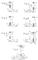
- reference number 10 a bond capillary, 11 a gold bond wire with a mini ball 12 on the lower free wire end, 13 one on the bond wire 11 attacking wire clip, 14 a component with a first bond point 17, 15 a lead frame, 16 a second Bond site on the lead frame or substrate, and 18 a Flame lance marked.
- the Bond head including bond capillary 10 with flamed bond wire ball or ball 12 on a first bond site 17 on a Component 14 lowered, corresponding to arrow 19 in FIG. 1.
- the bond capillary 10 is lowered with entrainment the ball 12 and thus corresponding entrainment of the bonding wire 11.
- the ball is then welded on 12 at the first bond point 17 on the component 14 below Heat addition defined contact pressure and / or ultrasound support.
- the bond head or the bond capillary 10 again started up (see arrow 20 in FIG. 3) and into a predetermined one 4 moved loop position under training a so-called bond wire loop 21.
- the bond capillary is located above the loop position second bond point 16.
- the bond capillary is then under corresponding entrainment of the bond wire 11 from the Loop position lowered again (see arrow 22 in Fig. 4). 5 then takes place in the lowered position welding the bond wire 11 to the second bond point 16 also with the addition of heat, defined contact pressure and / or ultrasound support.
- the bond wire 11 After the bond wire 11 has been torn off, it is brought up Bond capillary 10 lowered again until the free wire tip which has meanwhile been set on fire or swiveled flame lance or a corresponding stop contacted. Then the bondhead just needs it to be raised far until a predetermined distance reached between the free wire tip and the flame lance 18 is. In this way, the ball size can be permanent exact determination.
- the flame lance 18 leads the method only a movement in the direction of the double arrow 29 in FIG. 7.
- the actual tail-length 25 (Fig. 7) or the exact position of the free bond wire end above the second bond point 16 can be determined so that it is possible is the device for flaming the free bond wire end forming a new ball 12, namely the flame lance 18, opposite the free bond wire end or the wire tip in this way (see double arrow 29 in Fig.7) that the flame lance 18 always a predetermined Has distance to the bond wire tip. Then it will be the flame lance 18 activated (flame spark 27), so that the tail 25 deforms into a new ball 12.
- A preferably serves as a drive for the wire clamp 13 Stepper motor.
- the distance covered by the wire clip 13 The distance until the bond wire 11 is torn off accordingly recorded in steps (clocks).
- the flame lance 18 moves up and down Direction of the double arrow 26 also by means of a Stepper motor, the counters of the two stepper motors are coupled to one another via a computer unit, so that the desired assignment of the flame lance 18 to the free Wire tip can be produced automatically or fully automatically is.
- a conventional contact sensor can be used in the method electrical (non-contact), mechanical or ultrasonic sensor to serve.
- the process can also determine whether at all a sufficiently long tail 25 is present. If so after predetermined lowering of the bondhead no contact to the flame lance 18 is made this means that the tail-length is too short to be sufficient to be able to train large ball 12.
Description
- Fig. 1 bis 7
- den prinzipiellen Verfahrensablauf des erfindungsgemäßen Ball-Bondverfahrens.
Claims (5)
- Ball-Bondverfahren, wie ein Golddraht-Bondverfahren, welches folgende Arbeitsschritte umfaßt:dadurch gekennzeichnet, daßa) Positionieren und Absenken einer Bond-Kapillare (10) mit einer abgeflammten Bonddraht-Kugel (Ball 12) am unteren, freien Ende eines Bonddrahtes (11) aus einer hochgefahrenen Ausgangsposition auf eine erste Bondstelle (17);b) Aufschweißen des Balls (12) unter Wärmezugabe, definiertem Anpreßdruck und/oder Ultraschallunterstützung;c) Hochfahren der Bond-Kapillare (10);d) Bildung einer Bonddraht-Schleife (21);e) Aufschweißen des Bonddrahtes (11) an einer zweiten Bondstelle (16) unter Wärmezugabe, definiertem Anpreßdruck und/oder Ultraschallunterstützung;f) Hochfahren der Bond-Kapillare (10) in eine vorgegebene tail-length-Position (28), Abreißen des Bonddrahtes (11) durch Ausübung eines Zuges auf diesen mittels einer am Bonddraht (11) angreifenden Drahtklammer (13) und anschließend Hochfahren der Bond-Kapillare (10) in die Ausgangsposition; sowieg) Abflammen des freien Bonddrahtendes unter Ausbildung eines neuen Balls (12),h) vor dem Abflammen des freien Bonddrahtendes eine als Einrichtung zum Abflammen des freien Bonddrahtendes vorgesehene Abflammlanze (18) in Abflammstellung gebracht bzw. eingeschwenkt wird;i) anschließend die Bond-Kapillare (10) soweit abgesenkt wird, bis das freie Bonddrahtende bzw. die Drahtspitze die Abflammlanze (18) oder ein dieser zugeordnetes Wegbegrenzungs-Element kontaktiert; undj) die Bond-Kapillare (10) so dann wieder um eine vorgegebene Wegstrecke soweit hochgefahren wird, bis das freie Bonddrahtende einen vorbestimmten Abstand von der Abflammlanze (18) aufweist.
- Verfahren nach Anspruch 1,
dadurch gekennzeichnet, daß
die Kontaktierung des freien Bonddrahtendes mittels eines elektrischen, mechanischen und/oder Ultraschall-Sensors festgestellt wird. - Vorrichtung zur Durchführung des Verfahrens nach einem der Ansprüche 1 oder 2, umfassend eine Bond-Kapillare (10) mit einem Bonddraht (11), die auf bzw. von Bondstellen (16, 17) zu- bzw. wegbewegbar ist, einer am Bonddraht (11) angreifenden Drahtklammer (13), die auf bzw. von den Bondstellen (16, 17) zu- bzw. wegbewegbar ist, und einer Einrichtung zum Anlegen einer elektrischen Spannung zwischen der Drahtklammer (13) und der einen Bondstelle (16),
dadurch gekennzeichnet, daß
der den Abriß des Bonddrahtes (11) bewirkenden Drahtklammer (13) ein Schrittantrieb zugeordnet ist, der mit einem Zählwerk gekoppelt ist, welches die von der Drahtklammer (13) zurückgelegte Wegstrecke bestimmt und für die erneute Bestimmung einer weiteren Wegstrecke auf Null einstellbar ist und daß ein Kontaktsensor vorgesehen ist, zum Feststellen eines Kontaktes zwischen dem freien Bonddrahtende und der Abflammlanze (18) oder einem dieser angeordneten Wegbegrenzungs-Element. - Vorrichtung nach Anspruch 3,
dadurch gekennzeichnet, daß
eine als Einrichtung zum Abflammen des freien Bonddrahtendes vorgesehene Abflammlanze (18) auf bzw. von den Bondstellen (16, 17) zu bzw. wegbewegbar ist, wobei der Abflammlanze (18) ein Schrittantrieb zugeordnet ist, der mit einem Zählwerk gekoppelt ist, welches die von der Abflammlanze (18) zurückgelegte Wegstrecke bestimmt und für die erneute Bestimmung einer weiteren Wegstrecke auf Null einstellbar ist. - Vorrichtung nach Anspruch 3 oder 4,
dadurch gekennzeichnet, daß
der Kontaktsensor als elektrischer, mechanischer oder Ultraschall-Sensor ausgebildet ist.
Applications Claiming Priority (3)
| Application Number | Priority Date | Filing Date | Title |
|---|---|---|---|
| DE3703694 | 1987-02-06 | ||
| DE19873703694 DE3703694A1 (de) | 1987-02-06 | 1987-02-06 | Ball-bondverfahren und vorrichtung zur durchfuehrung derselben |
| EP87907960A EP0299987B1 (de) | 1987-02-06 | 1987-12-09 | Ball-bondverfahren und vorrichtung zur durchführung derselben |
Related Parent Applications (2)
| Application Number | Title | Priority Date | Filing Date |
|---|---|---|---|
| EP87907960.6 Division | 1987-12-09 | ||
| EP87907960A Division EP0299987B1 (de) | 1987-02-06 | 1987-12-09 | Ball-bondverfahren und vorrichtung zur durchführung derselben |
Publications (3)
| Publication Number | Publication Date |
|---|---|
| EP0533164A2 EP0533164A2 (de) | 1993-03-24 |
| EP0533164A3 EP0533164A3 (en) | 1993-07-14 |
| EP0533164B1 true EP0533164B1 (de) | 1999-03-31 |
Family
ID=6320422
Family Applications (2)
| Application Number | Title | Priority Date | Filing Date |
|---|---|---|---|
| EP87907960A Expired - Lifetime EP0299987B1 (de) | 1987-02-06 | 1987-12-09 | Ball-bondverfahren und vorrichtung zur durchführung derselben |
| EP92115937A Expired - Lifetime EP0533164B1 (de) | 1987-02-06 | 1987-12-09 | Ball-Bondverfahren und Vorrichtung zur Durchführung desselben |
Family Applications Before (1)
| Application Number | Title | Priority Date | Filing Date |
|---|---|---|---|
| EP87907960A Expired - Lifetime EP0299987B1 (de) | 1987-02-06 | 1987-12-09 | Ball-bondverfahren und vorrichtung zur durchführung derselben |
Country Status (7)
| Country | Link |
|---|---|
| US (1) | US4925083A (de) |
| EP (2) | EP0299987B1 (de) |
| JP (1) | JPH01502066A (de) |
| KR (1) | KR960005549B1 (de) |
| AT (2) | ATE178431T1 (de) |
| DE (3) | DE3703694A1 (de) |
| WO (1) | WO1988005960A1 (de) |
Families Citing this family (94)
| Publication number | Priority date | Publication date | Assignee | Title |
|---|---|---|---|---|
| US5285949A (en) * | 1987-01-26 | 1994-02-15 | Hitachi, Ltd. | Wire-bonding method, wire-bonding apparatus, and semiconductor device produced by the wire-bonding method |
| US5014111A (en) * | 1987-12-08 | 1991-05-07 | Matsushita Electric Industrial Co., Ltd. | Electrical contact bump and a package provided with the same |
| US5326015A (en) * | 1993-03-29 | 1994-07-05 | Kulicke And Soffa Investments, Inc. | Wire bonder tail length monitor |
| DE4335468A1 (de) * | 1993-10-18 | 1995-04-20 | F&K Delvotec Bondtechnik Gmbh | Vorrichtung und Verfahren zum Drahtbonden |
| US5683255A (en) * | 1993-12-03 | 1997-11-04 | Menze; Marion John | Radio frequency connector assembly |
| US5868300A (en) * | 1995-06-29 | 1999-02-09 | Orthodyne Electronics Corporation | Articulated wire bonder |
| US5874354A (en) * | 1995-09-26 | 1999-02-23 | Siemens Aktiengesellschaft | Method for electrically connecting a semiconductor chip to at least one contact surface and smart card module and smart card produced by the method |
| DE29608277U1 (de) * | 1996-04-30 | 1996-09-19 | F&K Delvotec Bondtechnik Gmbh | Vorrichtung zum Ball-Bonden |
| US6098868A (en) * | 1997-05-23 | 2000-08-08 | Masushita Electric Industrial Co., Ltd. | Bump forming method and bump bonder |
| DE19812706A1 (de) * | 1998-03-23 | 1999-10-07 | F&K Delvotec Bondtechnik Gmbh | Verfahren und Vorrichtung zum "ball-bonden" |
| JP2001189340A (ja) * | 1999-12-28 | 2001-07-10 | Shinkawa Ltd | ワイヤボンデイング方法及びその装置 |
| DE10035175C1 (de) * | 2000-07-19 | 2002-01-03 | Fraunhofer Ges Forschung | Verfahren zur Herstellung einer elektrischen und/oder mechanischen Verbindung von flexiblen Dünnfilmsubstraten |
| US6350632B1 (en) | 2000-09-20 | 2002-02-26 | Charles W. C. Lin | Semiconductor chip assembly with ball bond connection joint |
| US6350386B1 (en) | 2000-09-20 | 2002-02-26 | Charles W. C. Lin | Method of making a support circuit with a tapered through-hole for a semiconductor chip assembly |
| US6511865B1 (en) | 2000-09-20 | 2003-01-28 | Charles W. C. Lin | Method for forming a ball bond connection joint on a conductive trace and conductive pad in a semiconductor chip assembly |
| US6544813B1 (en) | 2000-10-02 | 2003-04-08 | Charles W. C. Lin | Method of making a semiconductor chip assembly with a conductive trace subtractively formed before and after chip attachment |
| US6448108B1 (en) | 2000-10-02 | 2002-09-10 | Charles W. C. Lin | Method of making a semiconductor chip assembly with a conductive trace subtractively formed before and after chip attachment |
| US7319265B1 (en) | 2000-10-13 | 2008-01-15 | Bridge Semiconductor Corporation | Semiconductor chip assembly with precision-formed metal pillar |
| US6876072B1 (en) | 2000-10-13 | 2005-04-05 | Bridge Semiconductor Corporation | Semiconductor chip assembly with chip in substrate cavity |
| US6576539B1 (en) | 2000-10-13 | 2003-06-10 | Charles W.C. Lin | Semiconductor chip assembly with interlocked conductive trace |
| US7264991B1 (en) | 2000-10-13 | 2007-09-04 | Bridge Semiconductor Corporation | Method of connecting a conductive trace to a semiconductor chip using conductive adhesive |
| US7071089B1 (en) | 2000-10-13 | 2006-07-04 | Bridge Semiconductor Corporation | Method of making a semiconductor chip assembly with a carved bumped terminal |
| US7414319B2 (en) * | 2000-10-13 | 2008-08-19 | Bridge Semiconductor Corporation | Semiconductor chip assembly with metal containment wall and solder terminal |
| US7190080B1 (en) | 2000-10-13 | 2007-03-13 | Bridge Semiconductor Corporation | Semiconductor chip assembly with embedded metal pillar |
| US6908788B1 (en) | 2000-10-13 | 2005-06-21 | Bridge Semiconductor Corporation | Method of connecting a conductive trace to a semiconductor chip using a metal base |
| US7262082B1 (en) | 2000-10-13 | 2007-08-28 | Bridge Semiconductor Corporation | Method of making a three-dimensional stacked semiconductor package with a metal pillar and a conductive interconnect in an encapsulant aperture |
| US6949408B1 (en) | 2000-10-13 | 2005-09-27 | Bridge Semiconductor Corporation | Method of connecting a conductive trace and an insulative base to a semiconductor chip using multiple etch steps |
| US6440835B1 (en) | 2000-10-13 | 2002-08-27 | Charles W. C. Lin | Method of connecting a conductive trace to a semiconductor chip |
| US6667229B1 (en) | 2000-10-13 | 2003-12-23 | Bridge Semiconductor Corporation | Method of connecting a bumped compliant conductive trace and an insulative base to a semiconductor chip |
| US6492252B1 (en) | 2000-10-13 | 2002-12-10 | Bridge Semiconductor Corporation | Method of connecting a bumped conductive trace to a semiconductor chip |
| US6740576B1 (en) | 2000-10-13 | 2004-05-25 | Bridge Semiconductor Corporation | Method of making a contact terminal with a plated metal peripheral sidewall portion for a semiconductor chip assembly |
| US7132741B1 (en) | 2000-10-13 | 2006-11-07 | Bridge Semiconductor Corporation | Semiconductor chip assembly with carved bumped terminal |
| US7009297B1 (en) | 2000-10-13 | 2006-03-07 | Bridge Semiconductor Corporation | Semiconductor chip assembly with embedded metal particle |
| US6699780B1 (en) | 2000-10-13 | 2004-03-02 | Bridge Semiconductor Corporation | Method of connecting a conductive trace to a semiconductor chip using plasma undercut etching |
| US6673710B1 (en) | 2000-10-13 | 2004-01-06 | Bridge Semiconductor Corporation | Method of connecting a conductive trace and an insulative base to a semiconductor chip |
| US6984576B1 (en) | 2000-10-13 | 2006-01-10 | Bridge Semiconductor Corporation | Method of connecting an additively and subtractively formed conductive trace and an insulative base to a semiconductor chip |
| US7094676B1 (en) | 2000-10-13 | 2006-08-22 | Bridge Semiconductor Corporation | Semiconductor chip assembly with embedded metal pillar |
| US6872591B1 (en) | 2000-10-13 | 2005-03-29 | Bridge Semiconductor Corporation | Method of making a semiconductor chip assembly with a conductive trace and a substrate |
| US6548393B1 (en) | 2000-10-13 | 2003-04-15 | Charles W. C. Lin | Semiconductor chip assembly with hardened connection joint |
| US7129575B1 (en) | 2000-10-13 | 2006-10-31 | Bridge Semiconductor Corporation | Semiconductor chip assembly with bumped metal pillar |
| US7075186B1 (en) | 2000-10-13 | 2006-07-11 | Bridge Semiconductor Corporation | Semiconductor chip assembly with interlocked contact terminal |
| US6576493B1 (en) | 2000-10-13 | 2003-06-10 | Bridge Semiconductor Corporation | Method of connecting a conductive trace and an insulative base to a semiconductor chip using multiple etch steps |
| US6537851B1 (en) | 2000-10-13 | 2003-03-25 | Bridge Semiconductor Corporation | Method of connecting a bumped compliant conductive trace to a semiconductor chip |
| US7129113B1 (en) | 2000-10-13 | 2006-10-31 | Bridge Semiconductor Corporation | Method of making a three-dimensional stacked semiconductor package with a metal pillar in an encapsulant aperture |
| US6444489B1 (en) | 2000-12-15 | 2002-09-03 | Charles W. C. Lin | Semiconductor chip assembly with bumped molded substrate |
| US6653170B1 (en) | 2001-02-06 | 2003-11-25 | Charles W. C. Lin | Semiconductor chip assembly with elongated wire ball bonded to chip and electrolessly plated to support circuit |
| US7993983B1 (en) | 2003-11-17 | 2011-08-09 | Bridge Semiconductor Corporation | Method of making a semiconductor chip assembly with chip and encapsulant grinding |
| US7538415B1 (en) | 2003-11-20 | 2009-05-26 | Bridge Semiconductor Corporation | Semiconductor chip assembly with bumped terminal, filler and insulative base |
| US7425759B1 (en) | 2003-11-20 | 2008-09-16 | Bridge Semiconductor Corporation | Semiconductor chip assembly with bumped terminal and filler |
| KR101313391B1 (ko) | 2004-11-03 | 2013-10-01 | 테세라, 인코포레이티드 | 적층형 패키징 |
| US7446419B1 (en) | 2004-11-10 | 2008-11-04 | Bridge Semiconductor Corporation | Semiconductor chip assembly with welded metal pillar of stacked metal balls |
| US7268421B1 (en) | 2004-11-10 | 2007-09-11 | Bridge Semiconductor Corporation | Semiconductor chip assembly with welded metal pillar that includes enlarged ball bond |
| US7750483B1 (en) | 2004-11-10 | 2010-07-06 | Bridge Semiconductor Corporation | Semiconductor chip assembly with welded metal pillar and enlarged plated contact terminal |
| US8058101B2 (en) | 2005-12-23 | 2011-11-15 | Tessera, Inc. | Microelectronic packages and methods therefor |
| JP4679427B2 (ja) * | 2006-04-24 | 2011-04-27 | 株式会社新川 | ボンディング装置のテールワイヤ切断方法及びプログラム |
| EP1897648B1 (de) | 2006-09-05 | 2010-06-30 | Technische Universität Berlin | Verfahren und Vorrichtung zur Regelung der Herstellung von Drahtbondverbindungen |
| US7494843B1 (en) | 2006-12-26 | 2009-02-24 | Bridge Semiconductor Corporation | Method of making a semiconductor chip assembly with thermal conductor and encapsulant grinding |
| US7811863B1 (en) | 2006-10-26 | 2010-10-12 | Bridge Semiconductor Corporation | Method of making a semiconductor chip assembly with metal pillar and encapsulant grinding and heat sink attachment |
| US7896218B2 (en) * | 2007-06-28 | 2011-03-01 | Western Digital Technologies, Inc. | Apparatus and method for conductive metal ball bonding with electrostatic discharge detection |
| US8020290B2 (en) * | 2009-06-14 | 2011-09-20 | Jayna Sheats | Processes for IC fabrication |
| US8482111B2 (en) | 2010-07-19 | 2013-07-09 | Tessera, Inc. | Stackable molded microelectronic packages |
| KR101128063B1 (ko) | 2011-05-03 | 2012-04-23 | 테세라, 인코포레이티드 | 캡슐화 층의 표면에 와이어 본드를 구비하는 패키지 적층형 어셈블리 |
| US9105483B2 (en) | 2011-10-17 | 2015-08-11 | Invensas Corporation | Package-on-package assembly with wire bond vias |
| US8946757B2 (en) | 2012-02-17 | 2015-02-03 | Invensas Corporation | Heat spreading substrate with embedded interconnects |
| US8372741B1 (en) | 2012-02-24 | 2013-02-12 | Invensas Corporation | Method for package-on-package assembly with wire bonds to encapsulation surface |
| US8835228B2 (en) | 2012-05-22 | 2014-09-16 | Invensas Corporation | Substrate-less stackable package with wire-bond interconnect |
| US9391008B2 (en) | 2012-07-31 | 2016-07-12 | Invensas Corporation | Reconstituted wafer-level package DRAM |
| US9502390B2 (en) | 2012-08-03 | 2016-11-22 | Invensas Corporation | BVA interposer |
| US8878353B2 (en) | 2012-12-20 | 2014-11-04 | Invensas Corporation | Structure for microelectronic packaging with bond elements to encapsulation surface |
| US9136254B2 (en) | 2013-02-01 | 2015-09-15 | Invensas Corporation | Microelectronic package having wire bond vias and stiffening layer |
| TWI487046B (zh) * | 2013-04-03 | 2015-06-01 | 矽品精密工業股份有限公司 | 銲線之銲接方法 |
| TWI518816B (zh) * | 2013-07-04 | 2016-01-21 | 先進科技新加坡有限公司 | 用於在導線鍵合過程中測量無空氣球尺寸的方法和裝置 |
| US9167710B2 (en) | 2013-08-07 | 2015-10-20 | Invensas Corporation | Embedded packaging with preformed vias |
| US9685365B2 (en) * | 2013-08-08 | 2017-06-20 | Invensas Corporation | Method of forming a wire bond having a free end |
| US20150076714A1 (en) | 2013-09-16 | 2015-03-19 | Invensas Corporation | Microelectronic element with bond elements to encapsulation surface |
| US9263394B2 (en) | 2013-11-22 | 2016-02-16 | Invensas Corporation | Multiple bond via arrays of different wire heights on a same substrate |
| US9583456B2 (en) | 2013-11-22 | 2017-02-28 | Invensas Corporation | Multiple bond via arrays of different wire heights on a same substrate |
| US9379074B2 (en) | 2013-11-22 | 2016-06-28 | Invensas Corporation | Die stacks with one or more bond via arrays of wire bond wires and with one or more arrays of bump interconnects |
| US9583411B2 (en) | 2014-01-17 | 2017-02-28 | Invensas Corporation | Fine pitch BVA using reconstituted wafer with area array accessible for testing |
| US10381326B2 (en) | 2014-05-28 | 2019-08-13 | Invensas Corporation | Structure and method for integrated circuits packaging with increased density |
| US9735084B2 (en) | 2014-12-11 | 2017-08-15 | Invensas Corporation | Bond via array for thermal conductivity |
| US9888579B2 (en) | 2015-03-05 | 2018-02-06 | Invensas Corporation | Pressing of wire bond wire tips to provide bent-over tips |
| US9502372B1 (en) | 2015-04-30 | 2016-11-22 | Invensas Corporation | Wafer-level packaging using wire bond wires in place of a redistribution layer |
| US9761554B2 (en) | 2015-05-07 | 2017-09-12 | Invensas Corporation | Ball bonding metal wire bond wires to metal pads |
| US9881895B2 (en) * | 2015-08-18 | 2018-01-30 | Lockheed Martin Corporation | Wire bonding methods and systems incorporating metal nanoparticles |
| US10490528B2 (en) | 2015-10-12 | 2019-11-26 | Invensas Corporation | Embedded wire bond wires |
| US9490222B1 (en) | 2015-10-12 | 2016-11-08 | Invensas Corporation | Wire bond wires for interference shielding |
| US10332854B2 (en) | 2015-10-23 | 2019-06-25 | Invensas Corporation | Anchoring structure of fine pitch bva |
| US10181457B2 (en) | 2015-10-26 | 2019-01-15 | Invensas Corporation | Microelectronic package for wafer-level chip scale packaging with fan-out |
| US10043779B2 (en) | 2015-11-17 | 2018-08-07 | Invensas Corporation | Packaged microelectronic device for a package-on-package device |
| US9659848B1 (en) | 2015-11-18 | 2017-05-23 | Invensas Corporation | Stiffened wires for offset BVA |
| US9984992B2 (en) | 2015-12-30 | 2018-05-29 | Invensas Corporation | Embedded wire bond wires for vertical integration with separate surface mount and wire bond mounting surfaces |
| US9935075B2 (en) | 2016-07-29 | 2018-04-03 | Invensas Corporation | Wire bonding method and apparatus for electromagnetic interference shielding |
| US10299368B2 (en) | 2016-12-21 | 2019-05-21 | Invensas Corporation | Surface integrated waveguides and circuit structures therefor |
Family Cites Families (12)
| Publication number | Priority date | Publication date | Assignee | Title |
|---|---|---|---|---|
| US3767101A (en) * | 1972-01-26 | 1973-10-23 | Hughes Aircraft Co | Pulse vibrator for thermocompression bonding |
| US3863827A (en) * | 1972-11-10 | 1975-02-04 | Mech El Ind Inc | Tailless wire bonder |
| US3941486A (en) * | 1974-06-03 | 1976-03-02 | The Computervision Corporation | Wire bonder |
| US3934108A (en) * | 1974-09-16 | 1976-01-20 | Uthe Technology, Inc. | Lead bonding method and apparatus |
| GB1468974A (en) * | 1975-05-23 | 1977-03-30 | Ferranti Ltd | Manufacture of semiconductor devices |
| US4109846A (en) * | 1977-05-17 | 1978-08-29 | Sola Basic Industries, Inc. | Automatic height sensor for semiconductor bonding tool, wafer probe or the like |
| US4213556A (en) * | 1978-10-02 | 1980-07-22 | General Motors Corporation | Method and apparatus to detect automatic wire bonder failure |
| US4266710A (en) * | 1978-11-22 | 1981-05-12 | Kulicke And Soffa Industries Inc. | Wire bonding apparatus |
| DE3037735A1 (de) * | 1980-10-06 | 1982-05-13 | TS-Electronic Vertriebs-GmbH, 8000 München | Kontaktierverfahren und kontaktiermaschine zur durchfuehrung des verfahrens |
| JPS57211240A (en) * | 1981-06-22 | 1982-12-25 | Hitachi Ltd | Wire bonder |
| US4555052A (en) * | 1983-02-28 | 1985-11-26 | Fairchild Camera & Instrument Corporation | Lead wire bond attempt detection |
| US4586642A (en) * | 1985-05-13 | 1986-05-06 | Kulicke And Soffa Industries Inc. | Wire bond monitoring system |
-
1987
- 1987-02-06 DE DE19873703694 patent/DE3703694A1/de not_active Withdrawn
- 1987-12-09 AT AT92115937T patent/ATE178431T1/de not_active IP Right Cessation
- 1987-12-09 EP EP87907960A patent/EP0299987B1/de not_active Expired - Lifetime
- 1987-12-09 AT AT87907960T patent/ATE106607T1/de not_active IP Right Cessation
- 1987-12-09 JP JP63500228A patent/JPH01502066A/ja active Pending
- 1987-12-09 EP EP92115937A patent/EP0533164B1/de not_active Expired - Lifetime
- 1987-12-09 WO PCT/EP1987/000765 patent/WO1988005960A1/de active IP Right Grant
- 1987-12-09 KR KR1019880701243A patent/KR960005549B1/ko active IP Right Grant
- 1987-12-09 US US07/272,780 patent/US4925083A/en not_active Expired - Lifetime
- 1987-12-09 DE DE3752266T patent/DE3752266D1/de not_active Expired - Lifetime
- 1987-12-09 DE DE3789962T patent/DE3789962D1/de not_active Expired - Fee Related
Also Published As
| Publication number | Publication date |
|---|---|
| WO1988005960A1 (en) | 1988-08-11 |
| DE3789962D1 (de) | 1994-07-07 |
| EP0533164A2 (de) | 1993-03-24 |
| US4925083A (en) | 1990-05-15 |
| KR890700921A (ko) | 1989-04-28 |
| ATE106607T1 (de) | 1994-06-15 |
| ATE178431T1 (de) | 1999-04-15 |
| EP0299987B1 (de) | 1994-06-01 |
| EP0299987A1 (de) | 1989-01-25 |
| JPH01502066A (ja) | 1989-07-13 |
| EP0533164A3 (en) | 1993-07-14 |
| KR960005549B1 (ko) | 1996-04-26 |
| DE3703694A1 (de) | 1988-08-18 |
| DE3752266D1 (de) | 1999-05-06 |
Similar Documents
| Publication | Publication Date | Title |
|---|---|---|
| EP0533164B1 (de) | Ball-Bondverfahren und Vorrichtung zur Durchführung desselben | |
| DE19752319B4 (de) | Ultraschall-Drahtbondingvorrichtung mit einer Einrichtung zum Prüfen einer Bondverbindung und Verfahren zum Prüfen einer mittels eines Ultraschall-Drahtbondingwerkzeugs hergestellten Bondverbindung | |
| DE3333601C2 (de) | ||
| DE4016720A1 (de) | Verfahren und vorrichtung zum ultraschallbonden | |
| DE3810929C2 (de) | ||
| DE4205742A1 (de) | Haltezange fuer einen kern waehrend dem wickeln | |
| DE2032302A1 (de) | Verfahren und Vorrichtung zum Anbrin gen von Zuleitungen an metallisierten Be reichen von Halbleiteroberflachen | |
| EP0656310B1 (de) | Verfahren und Vorrichtung zur Herstellung eines Folienverbundes | |
| DE3933982C2 (de) | Kontaktierungsverfahren und Kontaktierungsvorrichtung | |
| DE102012112667A1 (de) | Verfahren und Vorrichtung zum Ausbilden eines Nagelbondhügels | |
| DE1514285C3 (de) | Verfahren zur Herstellung einer Halbleitervorrichtung | |
| CH682597A5 (de) | Kontaktierungsqualitäts-Analysator. | |
| DE4129933C2 (de) | Verfahren und Vorrichtung zum Drahtbonden | |
| EP1474266A1 (de) | Anordnung zum drahtbonden und verfahren zur herstellung einer bondverbindung | |
| DE19625638A1 (de) | Drahtbondingverfahren und -kopf | |
| DE3504422C2 (de) | ||
| DE102015017014B4 (de) | Anker mit Wicklungen und Verfahren zum Verbinden von Wicklungsenden des Ankers mit einer Anschlussklemme | |
| DE4307080A1 (de) | Verfahren und Vorrichtung zur Herstellung einer Spulenanordnung | |
| DE1465095B2 (de) | Verfahren und vorrichtung zum elektrischen verbinden zweier auf einer schaltplatte befindlicher anschlusszapfen | |
| DE1591226A1 (de) | Vorrichtung zur Formung und zum Aufsetzen von Kontaktbruecken auf elektrische Schaltungen | |
| DE3739955A1 (de) | Vorrichtung zur ultraschall-drahtkontaktierung | |
| DE1160110B (de) | Verfahren und Vorrichtung zum automatischen Aufbau von Halbleiterkristalldioden | |
| DE2343365A1 (de) | Elektroschweissgeraet | |
| DE4326478C2 (de) | Bondkopf für Ultraschall-Bonden | |
| DE2522022C3 (de) | Verfahren zum Anbringen einer Drahtverbindung zwischen einer Kontaktstelle auf einer Halbleiteranordnung und einem Zuführungsleiter |
Legal Events
| Date | Code | Title | Description |
|---|---|---|---|
| PUAI | Public reference made under article 153(3) epc to a published international application that has entered the european phase |
Free format text: ORIGINAL CODE: 0009012 |
|
| AC | Divisional application: reference to earlier application |
Ref document number: 299987 Country of ref document: EP |
|
| AK | Designated contracting states |
Kind code of ref document: A2 Designated state(s): AT BE CH DE FR GB IT LI NL SE |
|
| RIN1 | Information on inventor provided before grant (corrected) |
Inventor name: BIRGEL, WALTER Inventor name: FARASSAT, FARHAD |
|
| PUAL | Search report despatched |
Free format text: ORIGINAL CODE: 0009013 |
|
| AK | Designated contracting states |
Kind code of ref document: A3 Designated state(s): AT BE CH DE FR GB IT LI NL SE |
|
| 17P | Request for examination filed |
Effective date: 19940317 |
|
| 17Q | First examination report despatched |
Effective date: 19960619 |
|
| GRAG | Despatch of communication of intention to grant |
Free format text: ORIGINAL CODE: EPIDOS AGRA |
|
| GRAG | Despatch of communication of intention to grant |
Free format text: ORIGINAL CODE: EPIDOS AGRA |
|
| GRAH | Despatch of communication of intention to grant a patent |
Free format text: ORIGINAL CODE: EPIDOS IGRA |
|
| GRAH | Despatch of communication of intention to grant a patent |
Free format text: ORIGINAL CODE: EPIDOS IGRA |
|
| GRAA | (expected) grant |
Free format text: ORIGINAL CODE: 0009210 |
|
| RAP1 | Party data changed (applicant data changed or rights of an application transferred) |
Owner name: F & K DELVOTEC BONDTECHNIK GMBH |
|
| AC | Divisional application: reference to earlier application |
Ref document number: 299987 Country of ref document: EP |
|
| AK | Designated contracting states |
Kind code of ref document: B1 Designated state(s): AT BE CH DE FR GB IT LI NL SE |
|
| REF | Corresponds to: |
Ref document number: 178431 Country of ref document: AT Date of ref document: 19990415 Kind code of ref document: T |
|
| REG | Reference to a national code |
Ref country code: CH Ref legal event code: NV Representative=s name: RITSCHER & SEIFERT Ref country code: CH Ref legal event code: EP |
|
| REF | Corresponds to: |
Ref document number: 3752266 Country of ref document: DE Date of ref document: 19990506 |
|
| GBT | Gb: translation of ep patent filed (gb section 77(6)(a)/1977) |
Effective date: 19990610 |
|
| ET | Fr: translation filed | ||
| PLBE | No opposition filed within time limit |
Free format text: ORIGINAL CODE: 0009261 |
|
| STAA | Information on the status of an ep patent application or granted ep patent |
Free format text: STATUS: NO OPPOSITION FILED WITHIN TIME LIMIT |
|
| 26N | No opposition filed | ||
| REG | Reference to a national code |
Ref country code: GB Ref legal event code: IF02 |
|
| PGFP | Annual fee paid to national office [announced via postgrant information from national office to epo] |
Ref country code: GB Payment date: 20021118 Year of fee payment: 16 |
|
| PGFP | Annual fee paid to national office [announced via postgrant information from national office to epo] |
Ref country code: AT Payment date: 20021223 Year of fee payment: 16 |
|
| PGFP | Annual fee paid to national office [announced via postgrant information from national office to epo] |
Ref country code: SE Payment date: 20021227 Year of fee payment: 16 |
|
| PGFP | Annual fee paid to national office [announced via postgrant information from national office to epo] |
Ref country code: BE Payment date: 20030107 Year of fee payment: 16 |
|
| PG25 | Lapsed in a contracting state [announced via postgrant information from national office to epo] |
Ref country code: GB Free format text: LAPSE BECAUSE OF NON-PAYMENT OF DUE FEES Effective date: 20031209 Ref country code: AT Free format text: LAPSE BECAUSE OF NON-PAYMENT OF DUE FEES Effective date: 20031209 |
|
| PG25 | Lapsed in a contracting state [announced via postgrant information from national office to epo] |
Ref country code: SE Free format text: LAPSE BECAUSE OF NON-PAYMENT OF DUE FEES Effective date: 20031210 |
|
| PGFP | Annual fee paid to national office [announced via postgrant information from national office to epo] |
Ref country code: CH Payment date: 20031212 Year of fee payment: 17 |
|
| PGFP | Annual fee paid to national office [announced via postgrant information from national office to epo] |
Ref country code: NL Payment date: 20031217 Year of fee payment: 17 |
|
| PGFP | Annual fee paid to national office [announced via postgrant information from national office to epo] |
Ref country code: FR Payment date: 20031218 Year of fee payment: 17 |
|
| PG25 | Lapsed in a contracting state [announced via postgrant information from national office to epo] |
Ref country code: BE Free format text: LAPSE BECAUSE OF NON-PAYMENT OF DUE FEES Effective date: 20031231 |
|
| BERE | Be: lapsed |
Owner name: F & K *DELVOTEC BONDTECHNIK G.M.B.H. Effective date: 20031231 |
|
| GBPC | Gb: european patent ceased through non-payment of renewal fee |
Effective date: 20031209 |
|
| EUG | Se: european patent has lapsed | ||
| PG25 | Lapsed in a contracting state [announced via postgrant information from national office to epo] |
Ref country code: LI Free format text: LAPSE BECAUSE OF NON-PAYMENT OF DUE FEES Effective date: 20041231 Ref country code: CH Free format text: LAPSE BECAUSE OF NON-PAYMENT OF DUE FEES Effective date: 20041231 |
|
| PG25 | Lapsed in a contracting state [announced via postgrant information from national office to epo] |
Ref country code: NL Free format text: LAPSE BECAUSE OF NON-PAYMENT OF DUE FEES Effective date: 20050701 |
|
| REG | Reference to a national code |
Ref country code: CH Ref legal event code: PL |
|
| PG25 | Lapsed in a contracting state [announced via postgrant information from national office to epo] |
Ref country code: FR Free format text: LAPSE BECAUSE OF NON-PAYMENT OF DUE FEES Effective date: 20050831 |
|
| NLV4 | Nl: lapsed or anulled due to non-payment of the annual fee |
Effective date: 20050701 |
|
| REG | Reference to a national code |
Ref country code: FR Ref legal event code: ST |
|
| PG25 | Lapsed in a contracting state [announced via postgrant information from national office to epo] |
Ref country code: IT Free format text: LAPSE BECAUSE OF NON-PAYMENT OF DUE FEES;WARNING: LAPSES OF ITALIAN PATENTS WITH EFFECTIVE DATE BEFORE 2007 MAY HAVE OCCURRED AT ANY TIME BEFORE 2007. THE CORRECT EFFECTIVE DATE MAY BE DIFFERENT FROM THE ONE RECORDED. Effective date: 20051209 |
|
| PGFP | Annual fee paid to national office [announced via postgrant information from national office to epo] |
Ref country code: DE Payment date: 20070226 Year of fee payment: 20 |