EP0532897A2 - Method of reworking circuit panels, and circuit panels reworked thereby - Google Patents
Method of reworking circuit panels, and circuit panels reworked thereby Download PDFInfo
- Publication number
- EP0532897A2 EP0532897A2 EP92113570A EP92113570A EP0532897A2 EP 0532897 A2 EP0532897 A2 EP 0532897A2 EP 92113570 A EP92113570 A EP 92113570A EP 92113570 A EP92113570 A EP 92113570A EP 0532897 A2 EP0532897 A2 EP 0532897A2
- Authority
- EP
- European Patent Office
- Prior art keywords
- conformal
- dielectric
- polymeric
- circuitization
- layer
- Prior art date
- Legal status (The legal status is an assumption and is not a legal conclusion. Google has not performed a legal analysis and makes no representation as to the accuracy of the status listed.)
- Ceased
Links
Images
Classifications
-
- H—ELECTRICITY
- H01—ELECTRIC ELEMENTS
- H01L—SEMICONDUCTOR DEVICES NOT COVERED BY CLASS H10
- H01L21/00—Processes or apparatus adapted for the manufacture or treatment of semiconductor or solid state devices or of parts thereof
- H01L21/02—Manufacture or treatment of semiconductor devices or of parts thereof
- H01L21/04—Manufacture or treatment of semiconductor devices or of parts thereof the devices having at least one potential-jump barrier or surface barrier, e.g. PN junction, depletion layer or carrier concentration layer
- H01L21/48—Manufacture or treatment of parts, e.g. containers, prior to assembly of the devices, using processes not provided for in a single one of the subgroups H01L21/06 - H01L21/326
- H01L21/4814—Conductive parts
- H01L21/4846—Leads on or in insulating or insulated substrates, e.g. metallisation
- H01L21/485—Adaptation of interconnections, e.g. engineering charges, repair techniques
-
- H—ELECTRICITY
- H05—ELECTRIC TECHNIQUES NOT OTHERWISE PROVIDED FOR
- H05K—PRINTED CIRCUITS; CASINGS OR CONSTRUCTIONAL DETAILS OF ELECTRIC APPARATUS; MANUFACTURE OF ASSEMBLAGES OF ELECTRICAL COMPONENTS
- H05K3/00—Apparatus or processes for manufacturing printed circuits
- H05K3/46—Manufacturing multilayer circuits
- H05K3/4644—Manufacturing multilayer circuits by building the multilayer layer by layer, i.e. build-up multilayer circuits
- H05K3/4664—Adding a circuit layer by thick film methods, e.g. printing techniques or by other techniques for making conductive patterns by using pastes, inks or powders
-
- H—ELECTRICITY
- H05—ELECTRIC TECHNIQUES NOT OTHERWISE PROVIDED FOR
- H05K—PRINTED CIRCUITS; CASINGS OR CONSTRUCTIONAL DETAILS OF ELECTRIC APPARATUS; MANUFACTURE OF ASSEMBLAGES OF ELECTRICAL COMPONENTS
- H05K3/00—Apparatus or processes for manufacturing printed circuits
- H05K3/46—Manufacturing multilayer circuits
- H05K3/4685—Manufacturing of cross-over conductors
-
- Y—GENERAL TAGGING OF NEW TECHNOLOGICAL DEVELOPMENTS; GENERAL TAGGING OF CROSS-SECTIONAL TECHNOLOGIES SPANNING OVER SEVERAL SECTIONS OF THE IPC; TECHNICAL SUBJECTS COVERED BY FORMER USPC CROSS-REFERENCE ART COLLECTIONS [XRACs] AND DIGESTS
- Y10—TECHNICAL SUBJECTS COVERED BY FORMER USPC
- Y10T—TECHNICAL SUBJECTS COVERED BY FORMER US CLASSIFICATION
- Y10T29/00—Metal working
- Y10T29/49—Method of mechanical manufacture
- Y10T29/49002—Electrical device making
- Y10T29/49117—Conductor or circuit manufacturing
- Y10T29/49124—On flat or curved insulated base, e.g., printed circuit, etc.
- Y10T29/49155—Manufacturing circuit on or in base
Definitions
- the invention relates to circuit panels, and more particularly to a low cost method of post fabrication circuit changing, repairing, and rerouting.
- the method includes depositing (for example, screening) and curing one or more conformal, polymeric, dielectric coating on the surface of the panel, depositing conductive circuitization atop the cured conformal, polymeric, dielectric coating on the surface of the panel, and depositing a conformal, polymeric, dielectric coating atop the conductive circuitization layer.
- an electronic circuit contains many individual electronic circuit components, e.g., thousands or even millions of individual resistors, capacitors, inductors, diodes, and transistors. These individual circuit components are interconnected to form the circuits, and the individual circuits are further interconnected to form functional units. Power and signal distribution are done through these interconnections.
- the individual functional units require mechanical support and structural protection.
- the electrical circuits require electrical energy to function, and the removal of thermal energy to remain functional.
- Microelectronic packages such as, chips, modules, circuit cards, circuit boards, and combinations thereof, are used to protect, house, cool, and interconnect circuit components and circuits.
- circuit component to circuit component and circuit to circuit interconnection, heat dissipation, and mechanical protection are provided by an integrated circuit chip.
- This chip is referred to as the "zeroth" level of packaging, while the chip enclosed within its module is referred to as the first level of packaging.
- the second level of packaging is the circuit card.
- a circuit card performs at least four functions. First, the circuit card is employed because the total required circuit or bit count to perform a desired function exceeds the bit count of the zeroth and first level packages, i.e., the chip and chip modules. Second, the circuit card provides for signal interconnection with other circuit elements. Third, the second level package, i.e., the circuit card, provides a site for components that are not readily integrated into the first level package, i.e., the chip or module. These components include, e.g., capacitors, precision resistors, inductors, electromechanical switches, optical couplers, and the like. Fourth, attachment to the second level package provides for thermal management of the chip and module, i.e., heat dissipation. The primary purpose of the package remains electrical interconnection.
- reroute the electrical interconnection of the package that is, to reroute wiring leads. This may be the result of engineering changes, for example to accommodate new chip sets. Alternatively, rerouting may be necessary to correct manufacturing defects, for example to provide alternative signal pathways around unintentional open circuits, or to take unintentional short circuits out of the circuit network.
- circuit rerouting is made by abrading or "cutting” surface circuitization on one side of the panel, and running jumpers on the surface of the package between vias and through-holes previously connected by the now abraded or “cut” wiring.
- Other methods of rerouting involve joining insulated jumper wires to appropriate surface features on the package or panel.
- the process begins with an inspection of all incoming boards, followed by "cutting" all of the surface circuitization paths that are to be rerouted, for example because of engineering changes or defects.
- An epoxy dielectric is applied to the surface, except for openings at pads and lands.
- Conductor paths are screened onto the cured dielectric layer.
- 60:40 Pb:Sn solder paste is screened over the conductor paths. The process is completed by reflowing the solder.
- Picard Printed Circuit Card Rework Process
- IBM Technical Disclosure Bulletin Vol. 15 (No. 1) , pp. 246-247, (June 1972).
- Picard describes a rework process which uses two plastic sheets of PTFE, a dielectric, soldered to the microelectronic circuit panel. According to Picard, existing conductive paths are eliminated, for example, by milling, and two sheets of dielectric are used to implement new conductive paths.
- the first sheet which carries no circuitization, only pads and lands, is laid on the microelectronic circuit panel.
- the second sheet which carries circuitization on both surfaces is laid atop the first sheet.
- Both sheets have vias at locations corresponding to vias and lands on the microelectronic circuit panel.
- the needed vias on the circuitized sheet are "opened", and unneeded lands are eliminated, for example, by milling. All unneeded lands are eliminated from the uncircuitized sheet, except for those needed for reworks, changes, etc.
- the two sheets are aligned, and then soldered to the backside of the microelectronic circuit panel.
- Kozik An alternative rerouting process is shown in A.F. Kozik, Reworking of Component Bearing Cards , IBM Technical Disclosure Bulletin , Vol. 20 , No. 4 , pp. 1532-1533 (September 1977).
- Kozik describes reworking a microelectronic circuit panel by removing unneeded components, breaking wired connections, and thereafter adding new components to the component bearing surface of the microelectronic circuit panel. The changes are made on what Kozik characterizes as a new printed circuit.
- This new printed circuit is a sheet of a thin, flexible material, carrying a printed circuit pattern.
- the pattern is on the side of the flexible film facing away from the microelectronic circuit panel.
- the flexible film has a solder tab at each point at which it is to be bonded to a corresponding land on the microelectronic circuit panel, and soldered to the back surface of the panel.
- U.S. Patent 4,438,561 to Richard W. Mueller for METHOD OF REWORKING PRINTED CIRCUIT BOARDS describes a method of connecting electrically unconnected conductors on a microelectronic circuit panel with conductors on a flexible circuit element.
- the patent describes forming a flexible circuit element having a non-conductive substrate with a predetermined circuit pattern thereon.
- the flexible element has at least two through holes.
- This flexible circuit is aligned with respect to the circuit pattern, with the circuitization on the flexible element facing the pcb and being separated therefrom by an interleaved sheet of uncircuitized dielectric (element 24).
- An electrically conductive path is then established between the previously unconnected elements on the microelectronic circuit panel via the circuitization on the attached flexible carrier.
- the insulated wires can be semi-permanently attached to the rework layer.
- Semi-permanent adhesion is said to be achieved by a heat activated thermoplastic adhesive.
- the invention as claimed is intended to provide an inexpensive, low cost method of making engineering changes and repairs to microelectronic circuit panels.
- the method includes depositing sequentially depositing and curing one or more conformal, polymeric, dielectric coating layers on the surface of the panel, depositing conductive circuitization atop the conformal, polymeric, dielectric coating layer or layers on the surface of the panel, and depositing and curing a conformal, polymeric, dielectric top coating atop the conductive circuitization layer.
- a rerouted circuit panel having at least two surface features that are connected by a rerouted current lead.
- the current lead is formed of a dielectric encapsulated conductor electrically joining the two surface features.
- the dielectric encapsulated conductor structure includes a conformal, polymeric dielectric layer adherent to a surface of the circuit board, with a deposited conductor on the conformal, polymeric dielectric layer, and a conformal, polymeric dielectric layer deposited atop the deposited conductor.
- the invention disclosed herein is a deposited polymer thick film method of reworking a circuit panel (as a circuit board or card), and a reworked circuit panel structure including deposited thick film polymeric rerouting wires.
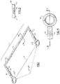
- FIGURES 1 through 5 The polymer thick film jumper wire structure adherent to and forming a new layer or partial layer or layers of the multi-layer circuit panel is shown in FIGURES 1 through 5.
- FIGURE 1 shows a microelectronic circuit panel 11 having original circuitization 21 thereon, shown between surface features, as lands 31a and 31b , or surface mount devices, or wire stubs or pins, or the like. It is desired to reroute circuitization between these two lands 31a and 31b , and remove circuitization 21 . According to the invention, rerouted circuitization 51 is provided on the microelectronic circuit panel 11 between the at least two surface features 31a and 31b .
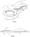
- the rerouted circuitization 51 shown in FIGURES 1, 2, 3, 4, and 5, includes a pair of terminators, as circular lands 53a and 53b superimposed over the panel lands 31a and 31b .
- the circular lands 53a and 53b include contact portions overlaid by a conductive wire 55 .
- This conductive wire 55 is carried by, and deposited on, a conformal polymeric dielectric layer or layers 57 and overlaid by a conformal polymeric dielectric top layer 59 .
- the dielectrics adherent to the underlying structure, allow a plurality of crossing rerouted circuitization wires 51 to be superimposed one above the other. In this way, a number of reroutings may be accomplished.
- FIGURE 2 is a cross-sectional view of the rerouted circuitization structure 51 through plane 2-2' of FIGURE 1.
- FIGURE 2 shows the underlying microelectronic circuit panel 11 , with the conductive wire 55 .
- This conductive wire 55 is carried by, and deposited on, a conformal first dielectric 57 and overlaid by a conformal second dielectric 59 .
- the conductive lands 53a , 53b are formed of conductive material, such as formed eyelets of Cu.
- the conductive wire 55 is a conductive deposit of a conductive metal, as copper or silver.
- the conductors 55 are typically about 254 ⁇ m to 508 ⁇ m (10 to 20 mils) wide and about 12.7 ⁇ m to 25.4 ⁇ m (0.5 to 1.0 mil) thick. They may be deposits or preforms of Cu or Ag.
- the conductors 55 are formed of "Minico 5000" silver paste, deposited between the bottom polymeric dielectric layer or layers 57 and the top polymeric dielectric layer 59 .
- the conformal bottom polymeric dielectric layer or layers 57 , and the conformal top polymeric dielectric 59 , an overcoat layer dielectric are typically about 12.7 to 25.4 ⁇ m (0.5 to 1.0 mil) thick, surrounding and encapsulating the conductive wire or layer 55 .
- Typical polymers include phenolics, epoxies, polyimides, and the like.
- the preferred polymeric dielectrics are characterized by a low dielectric constant, a relatively high dielectric breakdown voltage, and are substantially nonreactive with the cirtcuitization and the circuitization processes.
- the polymeric dielectric materials are preferably curable at about 200 degrees Centigrade or lower.
- the rerouting current lead 51 is formed of a dielectric 57 , 59 encapsulated conductor 55 electrically joining the two surface features 53a , 53b .
- the dielectric 57 , 59 encapsulated conductor 55 structure 51 includes a conformal, polymeric dielectric layer 57 adherent to a surface of the microelectronic circuit panel 11 , with a deposited conductor 55 on the conformal, polymeric dielectric layer, and a conformal, polymeric dielectric overcoat layer 59 deposited atop the deposited conductor 55 .
- the method includes depositing (for example, screening) a conformal, polymeric, dielectric carrier coating 57 on the surface of the microelectronic circuit panel 11 , depositing the conductive circuitization 55 atop the conformal, polymeric, dielectric carrier coating 57 on the surface of the panel 11 , and depositing a second conformal, polymeric, dielectric coating 59 atop the conductive circuitization layer 55 .
- the bottom dielectric is successively screened on as two or more layers, each individually screened and cured, one atop the other.
- the use of two or more sublayers 57 provides increased resistance to the development of short circuit paths between the deposited conductor 55 and the pre-existing surface circuitization 21 of the package.
- they are preferably about 12.7 to 17.8 ⁇ m (0.5 to 0.7 mils) thick.
- the rerouted circuitization 51 may be pre-formed as a lamination of two thermoset or thermoplastic polymeric layers 57 , 59 with a conductor 55 therebetween.
- the land eyelets 53a , 53b are at the ends of the encapsulated conductor.
- the invention provides an inexpensive, low cost method of and structure for making engineering changes and repairs to microelectronic circuit panels. In this way it is possible to effect engineering changes and wiring rerouting in the field, especially individual, customized engineering changes.
Landscapes
- Engineering & Computer Science (AREA)
- Manufacturing & Machinery (AREA)
- Microelectronics & Electronic Packaging (AREA)
- Ceramic Engineering (AREA)
- Physics & Mathematics (AREA)
- Condensed Matter Physics & Semiconductors (AREA)
- General Physics & Mathematics (AREA)
- Computer Hardware Design (AREA)
- Power Engineering (AREA)
- Production Of Multi-Layered Print Wiring Board (AREA)
- Manufacturing Of Printed Wiring (AREA)
Abstract
Description
- The invention relates to circuit panels, and more particularly to a low cost method of post fabrication circuit changing, repairing, and rerouting. The method includes depositing (for example, screening) and curing one or more conformal, polymeric, dielectric coating on the surface of the panel, depositing conductive circuitization atop the cured conformal, polymeric, dielectric coating on the surface of the panel, and depositing a conformal, polymeric, dielectric coating atop the conductive circuitization layer.
- The general structures and manufacturing processes for electronic packages, including the use of positive photoresists in the fabrication of electronic packages, are described in, for example, Donald P. Seraphim, Ronald Lasky, and Che-Yo Li, Principles of Electronic Packaging, McGraw-Hill Book Company, New York, New York, (1988), and Rao R. Tummala and Eugene J. Rymaszewski, Microelectronic Packaging Handbook, Van Nostrand Reinhold, New York, New York (1988), both of which are hereby incorporated herein by reference.
- As described by Seraphim et al., and Tummala et al., an electronic circuit contains many individual electronic circuit components, e.g., thousands or even millions of individual resistors, capacitors, inductors, diodes, and transistors. These individual circuit components are interconnected to form the circuits, and the individual circuits are further interconnected to form functional units. Power and signal distribution are done through these interconnections. The individual functional units require mechanical support and structural protection. The electrical circuits require electrical energy to function, and the removal of thermal energy to remain functional. Microelectronic packages, such as, chips, modules, circuit cards, circuit boards, and combinations thereof, are used to protect, house, cool, and interconnect circuit components and circuits.
- Within a single integrated circuit, circuit component to circuit component and circuit to circuit interconnection, heat dissipation, and mechanical protection are provided by an integrated circuit chip. This chip is referred to as the "zeroth" level of packaging, while the chip enclosed within its module is referred to as the first level of packaging.
- There is at least one further level of packaging. The second level of packaging is the circuit card. A circuit card performs at least four functions. First, the circuit card is employed because the total required circuit or bit count to perform a desired function exceeds the bit count of the zeroth and first level packages, i.e., the chip and chip modules. Second, the circuit card provides for signal interconnection with other circuit elements. Third, the second level package, i.e., the circuit card, provides a site for components that are not readily integrated into the first level package, i.e., the chip or module. These components include, e.g., capacitors, precision resistors, inductors, electromechanical switches, optical couplers, and the like. Fourth, attachment to the second level package provides for thermal management of the chip and module, i.e., heat dissipation. The primary purpose of the package remains electrical interconnection.
- At various times in the life-cycle of a microelectronic package, it is necessary to reroute the electrical interconnection of the package, that is, to reroute wiring leads. This may be the result of engineering changes, for example to accommodate new chip sets. Alternatively, rerouting may be necessary to correct manufacturing defects, for example to provide alternative signal pathways around unintentional open circuits, or to take unintentional short circuits out of the circuit network.
- Typically circuit rerouting is made by abrading or "cutting" surface circuitization on one side of the panel, and running jumpers on the surface of the package between vias and through-holes previously connected by the now abraded or "cut" wiring. Other methods of rerouting involve joining insulated jumper wires to appropriate surface features on the package or panel.
- One method of rerouting interconnections is described in J.Canavan, Screen Printing Engineering Changes on PCBs: Polymer Thick Film Materials Replace Hand Wiring, Circuits Manufacturing, Vol. 19 (No. 11), pages 22-26, November 1979. This paper describes a screen printing system, utilizing low temperature thick film materials, to overlay new circuits on the surface of finished, but unpopulated, microelectronic circuit packages. As described by Canavan, the process, called "WINK" (wire ink), allows conductive circuitization to be "screened" on the panel over a previously applied dielectric layer. This dielectric layer insulates the pre-existing circuitry from the re-routed circuitry.
- According to Canavan, the process begins with an inspection of all incoming boards, followed by "cutting" all of the surface circuitization paths that are to be rerouted, for example because of engineering changes or defects. An epoxy dielectric is applied to the surface, except for openings at pads and lands. Conductor paths are screened onto the cured dielectric layer. Next, 60:40 Pb:Sn solder paste is screened over the conductor paths. The process is completed by reflowing the solder.
- Another rerouting process is described by S. Picard, Printed Circuit Card Rework Process, IBM Technical Disclosure Bulletin, Vol. 15 (No. 1), pp. 246-247, (June 1972). Picard describes a rework process which uses two plastic sheets of PTFE, a dielectric, soldered to the microelectronic circuit panel. According to Picard, existing conductive paths are eliminated, for example, by milling, and two sheets of dielectric are used to implement new conductive paths.
- The first sheet, which carries no circuitization, only pads and lands, is laid on the microelectronic circuit panel. The second sheet, which carries circuitization on both surfaces is laid atop the first sheet. Both sheets have vias at locations corresponding to vias and lands on the microelectronic circuit panel. To define a new path, the needed vias on the circuitized sheet are "opened", and unneeded lands are eliminated, for example, by milling. All unneeded lands are eliminated from the uncircuitized sheet, except for those needed for reworks, changes, etc. The two sheets are aligned, and then soldered to the backside of the microelectronic circuit panel.
- An alternative rerouting process is shown in A.F. Kozik, Reworking of Component Bearing Cards, IBM Technical Disclosure Bulletin, Vol. 20, No. 4, pp. 1532-1533 (September 1977). Kozik describes reworking a microelectronic circuit panel by removing unneeded components, breaking wired connections, and thereafter adding new components to the component bearing surface of the microelectronic circuit panel. The changes are made on what Kozik characterizes as a new printed circuit.
- This new printed circuit is a sheet of a thin, flexible material, carrying a printed circuit pattern. The pattern is on the side of the flexible film facing away from the microelectronic circuit panel. The flexible film has a solder tab at each point at which it is to be bonded to a corresponding land on the microelectronic circuit panel, and soldered to the back surface of the panel.
- An alternative method of rerouting is described in W.D. Saucier, Circuit Overlay Adapter Assembly For Circuit Changes, IBM Technical Disclosure Bulletin, Vol. 18, No. 7, pp. 2050-2051 (December 1975). Saucier describes reworking a microelectronic circuit panel by connecting the panel to a circuitization carrying overlay. The circuitization carrying overlay is a non-adherent, "stand-off" panel, connected to appropriate lands on the panel by elastomeric pins.
- U.S. Patent 4,438,561 to Richard W. Mueller for METHOD OF REWORKING PRINTED CIRCUIT BOARDS describes a method of connecting electrically unconnected conductors on a microelectronic circuit panel with conductors on a flexible circuit element. The patent describes forming a flexible circuit element having a non-conductive substrate with a predetermined circuit pattern thereon. The flexible element has at least two through holes.
- This flexible circuit is aligned with respect to the circuit pattern, with the circuitization on the flexible element facing the pcb and being separated therefrom by an interleaved sheet of uncircuitized dielectric (element 24).
- An electrically conductive path is then established between the previously unconnected elements on the microelectronic circuit panel via the circuitization on the attached flexible carrier.
- A further alternative method of rerouting is described in U.S. Patent 4,310,810 to Thomas Currie for REWORKABLE MULTI-LAYER PRINTED CIRCUIT BOARD. Currie describes multi-layer microelectronic circuit panels having a rework layer. The rework layer has a plurality of insulated wires, that is, wires that are insulated from each other and the microelectronic circuit panel. The wires each have a characteristic impedance, Z, that matches the impedance of an internal conductive plane.
- The insulated wires can be semi-permanently attached to the rework layer. Semi-permanent adhesion is said to be achieved by a heat activated thermoplastic adhesive.
- A further method of rerouting is described in U.S. Patent 4,654,102 to Jean C. Wrey, Michel Jehay, and Andre Job for METHOD FOR CONNECTING PRINTED CIRCUIT BOARDS. In this patent preformed, high melting wire is formed, and deposited on the insulating panel.
- Another method of rerouting is described in U.S. Patent 4,731,704 to Anton Lochner for ARRANGEMENT FOR MODIFYING ELECTRICAL PRINTED CIRCUIT BOARDS. Lochner utilizes a non-conformal carrier, spaced from the microelectronic panel.
- The above described methods of rerouting wiring, repairing wiring, and making engineering changes fail to provide an inexpensive, low cost method of making engineering changes and repairs to microelectronic circuit panels,that can be carried out in the field, and are not particularly useful in making individual, customized engineering changes.
- The invention as claimed is intended to provide an inexpensive, low cost method of making engineering changes and repairs to microelectronic circuit panels.
- Disclosed is a method of reworking a circuit panel, i.e., a card or board, and a reworked circuit panel structure. The method includes depositing sequentially depositing and curing one or more conformal, polymeric, dielectric coating layers on the surface of the panel, depositing conductive circuitization atop the conformal, polymeric, dielectric coating layer or layers on the surface of the panel, and depositing and curing a conformal, polymeric, dielectric top coating atop the conductive circuitization layer.
- Also disclosed is a rerouted circuit panel having at least two surface features that are connected by a rerouted current lead. The current lead is formed of a dielectric encapsulated conductor electrically joining the two surface features. The dielectric encapsulated conductor structure includes a conformal, polymeric dielectric layer adherent to a surface of the circuit board, with a deposited conductor on the conformal, polymeric dielectric layer, and a conformal, polymeric dielectric layer deposited atop the deposited conductor.
- It is an advantage of the invention to provide a method of effecting engineering changes and wiring rerouting in the field.
- It is another advantage of the invention to provide a method of making individual, customized engineering changes.
- The invention may be understood by reference to the FIGURES appended hereto.
- For a better understanding of the present invention, together with further objects and advantages, preferred embodiments of the invention are described in the following with reference to the accompanying drawings, in which:
- FIGURE 1
- is a perspective view of the circuitization line to be replaced, the polymer thick film replacement circuitization line, and a section 2-2' through the polymer thick film replacement circuitization line.
- FIGURE 2
- is a cross-sectional view of the polymer thick film replacement line through plane 2-2'' of FIGURE 1.
- FIGURE 3
- is an expanded view of the land of the polymer thick film replacement line, showing the circuit lead, the replacement land, the carrier land, and the encapsulating polymer.
- FIGURE 4
- is a plan view of the carrier land, the replacement land, circuitization lead, and the encapsulating polymer.
- FIGURE 5
- is a cross sectional view of the carrier land, the replacement land, circuitization lead, and the encapsulating polymer.
- The invention disclosed herein is a deposited polymer thick film method of reworking a circuit panel (as a circuit board or card), and a reworked circuit panel structure including deposited thick film polymeric rerouting wires.
- The polymer thick film jumper wire structure adherent to and forming a new layer or partial layer or layers of the multi-layer circuit panel is shown in FIGURES 1 through 5.
- FIGURE 1 shows a microelectronic circuit panel 11 having
original circuitization 21 thereon, shown between surface features, as lands 31a and 31b, or surface mount devices, or wire stubs or pins, or the like. It is desired to reroute circuitization between these two lands 31a and 31b, and removecircuitization 21. According to the invention, reroutedcircuitization 51 is provided on the microelectronic circuit panel 11 between the at least two surface features 31a and 31b. - The rerouted
circuitization 51, shown in FIGURES 1, 2, 3, 4, and 5, includes a pair of terminators, as circular lands 53a and 53b superimposed over the panel lands 31a and 31b. The circular lands 53a and 53b include contact portions overlaid by aconductive wire 55. Thisconductive wire 55 is carried by, and deposited on, a conformal polymeric dielectric layer or layers 57 and overlaid by a conformal polymeric dielectrictop layer 59. - The dielectrics, adherent to the underlying structure, allow a plurality of crossing rerouted
circuitization wires 51 to be superimposed one above the other. In this way, a number of reroutings may be accomplished. - FIGURE 2 is a cross-sectional view of the rerouted
circuitization structure 51 through plane 2-2' of FIGURE 1. FIGURE 2 shows the underlying microelectronic circuit panel 11, with theconductive wire 55. Thisconductive wire 55 is carried by, and deposited on, a conformalfirst dielectric 57 and overlaid by a conformalsecond dielectric 59. - The conductive lands 53a, 53b, are formed of conductive material, such as formed eyelets of Cu. The
conductive wire 55, is a conductive deposit of a conductive metal, as copper or silver. Theconductors 55 are typically about 254 µm to 508 µm (10 to 20 mils) wide and about 12.7 µm to 25.4 µm (0.5 to 1.0 mil) thick. They may be deposits or preforms of Cu or Ag. In one embodiment theconductors 55 are formed of "Minico 5000" silver paste, deposited between the bottom polymeric dielectric layer or layers 57 and the toppolymeric dielectric layer 59. - The conformal bottom polymeric dielectric layer or layers 57, and the conformal top
polymeric dielectric 59, an overcoat layer dielectric, are typically about 12.7 to 25.4 µm (0.5 to 1.0 mil) thick, surrounding and encapsulating the conductive wire orlayer 55. Typical polymers include phenolics, epoxies, polyimides, and the like. The preferred polymeric dielectrics are characterized by a low dielectric constant, a relatively high dielectric breakdown voltage, and are substantially nonreactive with the cirtcuitization and the circuitization processes. The polymeric dielectric materials are preferably curable at about 200 degrees Centigrade or lower. - The rerouting
current lead 51 is formed of a dielectric 57, 59 encapsulatedconductor 55 electrically joining the two surface features 53a, 53b. The dielectric 57, 59 encapsulatedconductor 55structure 51 includes a conformal,polymeric dielectric layer 57 adherent to a surface of the microelectronic circuit panel 11, with a depositedconductor 55 on the conformal, polymeric dielectric layer, and a conformal, polymericdielectric overcoat layer 59 deposited atop the depositedconductor 55. - The method includes depositing (for example, screening) a conformal, polymeric,
dielectric carrier coating 57 on the surface of the microelectronic circuit panel 11, depositing theconductive circuitization 55 atop the conformal, polymeric,dielectric carrier coating 57 on the surface of the panel 11, and depositing a second conformal, polymeric,dielectric coating 59 atop theconductive circuitization layer 55. - According to a particularly preferred exemplification of the invention the bottom dielectric is successively screened on as two or more layers, each individually screened and cured, one atop the other. The use of two or more sublayers 57 provides increased resistance to the development of short circuit paths between the deposited
conductor 55 and thepre-existing surface circuitization 21 of the package. When two or more such sublayers are utilized, they are preferably about 12.7 to 17.8 µm (0.5 to 0.7 mils) thick. - According to a further embodiment of the invention, the rerouted
circuitization 51 may be pre-formed as a lamination of two thermoset or thermoplastic polymeric layers 57, 59 with aconductor 55 therebetween. The land eyelets 53a, 53b are at the ends of the encapsulated conductor. - The invention provides an inexpensive, low cost method of and structure for making engineering changes and repairs to microelectronic circuit panels. In this way it is possible to effect engineering changes and wiring rerouting in the field, especially individual, customized engineering changes.
Claims (10)
- A method of rerouting circuitization in a multilayer circuit panel having a first pair of conductive surface features at a surface thereof, said method comprising the steps of:A. depositing and curing at least one conformal, polymeric dielectric layer between a first surface feature and a second surface feature on the surface of the panel;B. providing circuitization on the conformal, polymeric dielectric layer between the first surface feature and the second surface feature;C. providing terminators electrically in contact with the conductive layer at the ends thereof over the surface features; andD. depositing and curing a top layer of dielectric overlaying at least the deposited circuitization and the terminators.
- The method of claim 1 comprising providing circuitization chosen from the group consisting of Cu and Ag.
- The method of claim 1 or 2 comprising depositing and curing a dielectric chosen from the group consisting of epoxies, phenolics, and polyimides.
- The method of any one of the preceding claims comprising successively depositing curing two bottom polymeric layers one atop the other.
- The method of any one of the preceding claims comprising joining the rerouting terminators to land surface features and/or surface mount device surface features
- The method of any one of the preceding claims comprising rerouting a second circuit between a second pair of surface features, said method including providing at least one conformal, polymeric dielectric layer between the second pair of surface features and overlaying at least a portion of the first rerouting; providing circuitizion on the conformal, polymeric dielectric layer between the second pair of surface features; providing terminators electrically in contact with the conductive layer at the ends thereof over the second pair of surface features; and providing a second layer of dielectric overlaying at least the second circuitization and the second terminators.
- A rerouted circuit panel having at least two surface features connected by a rerouted current lead, said current lead formed of a dielectric encapsulated conductor electrically joining the two surface features and comprising a conformal, polymeric dielectric bottom layer adherent to a surface of the circuit board, a conductor on the conformal, polymeric dielectric layer, and a conformal, polymeric dielectric layer atop the conductor.
- The rerouted circuit panel of claim 7 wherein the circuitization is chosen from the group consisting of Cu and Ag.
- The rerouted circuit panel of claim 7 or 8 wherein the dielectric is chosen from the group consisting of epoxies, phenolics, and polyimides.
- The rerouted circuit panel of any one of the preceding claims 7 to 9 wherein the polymeric bottom layer comprises at least two sub-layers, one atop the other.
Applications Claiming Priority (2)
| Application Number | Priority Date | Filing Date | Title |
|---|---|---|---|
| US07/762,201 US5214250A (en) | 1991-09-19 | 1991-09-19 | Method of reworking circuit panels, and circuit panels reworked thereby |
| US762201 | 1991-09-19 |
Publications (2)
| Publication Number | Publication Date |
|---|---|
| EP0532897A2 true EP0532897A2 (en) | 1993-03-24 |
| EP0532897A3 EP0532897A3 (en) | 1993-07-21 |
Family
ID=25064386
Family Applications (1)
| Application Number | Title | Priority Date | Filing Date |
|---|---|---|---|
| EP19920113570 Ceased EP0532897A3 (en) | 1991-09-19 | 1992-08-10 | Method of reworking circuit panels, and circuit panels reworked thereby |
Country Status (3)
| Country | Link |
|---|---|
| US (1) | US5214250A (en) |
| EP (1) | EP0532897A3 (en) |
| JP (1) | JPH0779196B2 (en) |
Cited By (2)
| Publication number | Priority date | Publication date | Assignee | Title |
|---|---|---|---|---|
| EP0613330A1 (en) * | 1992-11-09 | 1994-08-31 | Siemens Aktiengesellschaft | Discrete wiring method for printed circuit boards and/or electronic component assemblies |
| EP1075171A1 (en) * | 1999-07-31 | 2001-02-07 | Mannesmann VDO Aktiengesellschaft | Circuit board |
Families Citing this family (19)
| Publication number | Priority date | Publication date | Assignee | Title |
|---|---|---|---|---|
| JP2856240B2 (en) * | 1992-10-30 | 1999-02-10 | インターナショナル・ビジネス・マシーンズ・コーポレイション | How to rework a printed circuit board |
| US5834705A (en) * | 1994-03-04 | 1998-11-10 | Silicon Graphics, Inc. | Arrangement for modifying eletrical printed circuit boards |
| US6307162B1 (en) | 1996-12-09 | 2001-10-23 | International Business Machines Corporation | Integrated circuit wiring |
| US6097884A (en) * | 1997-12-08 | 2000-08-01 | Lsi Logic Corporation | Probe points and markers for critical paths and integrated circuits |
| US20030042295A1 (en) * | 2001-08-30 | 2003-03-06 | Wong Marvin G. | Self-adhesive flexible repair circuit |
| US7297572B2 (en) * | 2001-09-07 | 2007-11-20 | Hynix Semiconductor, Inc. | Fabrication method for electronic system modules |
| US6881609B2 (en) * | 2001-09-07 | 2005-04-19 | Peter C. Salmon | Component connections using bumps and wells |
| US6927471B2 (en) * | 2001-09-07 | 2005-08-09 | Peter C. Salmon | Electronic system modules and method of fabrication |
| US7505862B2 (en) * | 2003-03-07 | 2009-03-17 | Salmon Technologies, Llc | Apparatus and method for testing electronic systems |
| US7408258B2 (en) * | 2003-08-20 | 2008-08-05 | Salmon Technologies, Llc | Interconnection circuit and electronic module utilizing same |
| US20050184376A1 (en) * | 2004-02-19 | 2005-08-25 | Salmon Peter C. | System in package |
| US20050255722A1 (en) * | 2004-05-07 | 2005-11-17 | Salmon Peter C | Micro blade assembly |
| US7427809B2 (en) * | 2004-12-16 | 2008-09-23 | Salmon Technologies, Llc | Repairable three-dimensional semiconductor subsystem |
| US20070007983A1 (en) * | 2005-01-06 | 2007-01-11 | Salmon Peter C | Semiconductor wafer tester |
| US20070023904A1 (en) * | 2005-08-01 | 2007-02-01 | Salmon Peter C | Electro-optic interconnection apparatus and method |
| US7586747B2 (en) * | 2005-08-01 | 2009-09-08 | Salmon Technologies, Llc. | Scalable subsystem architecture having integrated cooling channels |
| US20070023923A1 (en) * | 2005-08-01 | 2007-02-01 | Salmon Peter C | Flip chip interface including a mixed array of heat bumps and signal bumps |
| US20070023889A1 (en) * | 2005-08-01 | 2007-02-01 | Salmon Peter C | Copper substrate with feedthroughs and interconnection circuits |
| US7351115B1 (en) | 2007-01-17 | 2008-04-01 | International Business Machines Corporation | Method for modifying an electrical connector |
Citations (2)
| Publication number | Priority date | Publication date | Assignee | Title |
|---|---|---|---|---|
| US4775573A (en) * | 1987-04-03 | 1988-10-04 | West-Tronics, Inc. | Multilayer PC board using polymer thick films |
| CA1249064A (en) * | 1987-07-06 | 1989-01-17 | Reginald B.P. Bennett | Process for application of overlay conductors to surface of printed circuit board assemblies |
Family Cites Families (8)
| Publication number | Priority date | Publication date | Assignee | Title |
|---|---|---|---|---|
| US4310811A (en) * | 1980-03-17 | 1982-01-12 | Sperry Corporation | Reworkable multi-layer printed circuit board |
| JPS56169576U (en) * | 1980-05-19 | 1981-12-15 | ||
| US4438561A (en) * | 1981-10-01 | 1984-03-27 | Rogers Corporation | Method of reworking printed circuit boards |
| GB2124835B (en) * | 1982-08-03 | 1986-04-30 | Burroughs Corp | Current printed circuit boards |
| DE3432360A1 (en) * | 1984-09-03 | 1986-03-13 | Siemens AG, 1000 Berlin und 8000 München | METHOD FOR MODIFYING AN ELECTRIC FLAT ASSEMBLY |
| US4864723A (en) * | 1986-07-01 | 1989-09-12 | Preleg, Inc. | Electrical circuit modification method |
| US4866507A (en) * | 1986-05-19 | 1989-09-12 | International Business Machines Corporation | Module for packaging semiconductor integrated circuit chips on a base substrate |
| JPH0271591A (en) * | 1988-09-07 | 1990-03-12 | Fujitsu Ltd | Reconditioning of circuit substrate |
-
1991
- 1991-09-19 US US07/762,201 patent/US5214250A/en not_active Expired - Fee Related
-
1992
- 1992-08-10 EP EP19920113570 patent/EP0532897A3/en not_active Ceased
- 1992-08-15 JP JP4238995A patent/JPH0779196B2/en not_active Expired - Lifetime
Patent Citations (2)
| Publication number | Priority date | Publication date | Assignee | Title |
|---|---|---|---|---|
| US4775573A (en) * | 1987-04-03 | 1988-10-04 | West-Tronics, Inc. | Multilayer PC board using polymer thick films |
| CA1249064A (en) * | 1987-07-06 | 1989-01-17 | Reginald B.P. Bennett | Process for application of overlay conductors to surface of printed circuit board assemblies |
Non-Patent Citations (1)
| Title |
|---|
| CIRCUITS MANUFACTURING vol. 19, no. 11, November 1979, pages 22 - 26 J. CANAVAN 'Screen printing engineering changes on PCBs' * |
Cited By (2)
| Publication number | Priority date | Publication date | Assignee | Title |
|---|---|---|---|---|
| EP0613330A1 (en) * | 1992-11-09 | 1994-08-31 | Siemens Aktiengesellschaft | Discrete wiring method for printed circuit boards and/or electronic component assemblies |
| EP1075171A1 (en) * | 1999-07-31 | 2001-02-07 | Mannesmann VDO Aktiengesellschaft | Circuit board |
Also Published As
| Publication number | Publication date |
|---|---|
| JPH06169177A (en) | 1994-06-14 |
| JPH0779196B2 (en) | 1995-08-23 |
| EP0532897A3 (en) | 1993-07-21 |
| US5214250A (en) | 1993-05-25 |
Similar Documents
| Publication | Publication Date | Title |
|---|---|---|
| US5214250A (en) | Method of reworking circuit panels, and circuit panels reworked thereby | |
| US5401913A (en) | Electrical interconnections between adjacent circuit board layers of a multi-layer circuit board | |
| US5527741A (en) | Fabrication and structures of circuit modules with flexible interconnect layers | |
| US7923828B2 (en) | Structure and method of making interconnect element, and multilayer wiring board including the interconnect element | |
| US5428190A (en) | Rigid-flex board with anisotropic interconnect and method of manufacture | |
| US6219253B1 (en) | Molded electronic package, method of preparation using build up technology and method of shielding | |
| US5412539A (en) | Multichip module with a mandrel-produced interconnecting decal | |
| EP0400332B1 (en) | Thin film multilayer laminate interconnection board assembly method | |
| US4970106A (en) | Thin film multilayer laminate interconnection board | |
| US7006359B2 (en) | Modular electronic assembly and method of making | |
| EP0471938A1 (en) | High circuit density thermal carrier | |
| US6427323B2 (en) | Method for producing conductor interconnect with dendrites | |
| EP1123565B1 (en) | Embedded capacitor multi-chip modules | |
| US20030141600A1 (en) | Apparatus and method of manufacturing printed circuit boards | |
| EP0521720A1 (en) | Heat-dissipating multi-layer circuit board | |
| GB2204184A (en) | Mounting electronic components on substrates | |
| US6897078B2 (en) | Programmable multi-chip module | |
| KR100301107B1 (en) | Multichip module substrate and method of manufacturing the same | |
| KR20020054112A (en) | Fabrication method of Mulichip module substrate with embedded passive components | |
| EP0525217A1 (en) | Carrier for electronic components |
Legal Events
| Date | Code | Title | Description |
|---|---|---|---|
| PUAI | Public reference made under article 153(3) epc to a published international application that has entered the european phase |
Free format text: ORIGINAL CODE: 0009012 |
|
| AK | Designated contracting states |
Kind code of ref document: A2 Designated state(s): DE FR GB |
|
| PUAL | Search report despatched |
Free format text: ORIGINAL CODE: 0009013 |
|
| RHK1 | Main classification (correction) |
Ipc: H05K 3/22 |
|
| AK | Designated contracting states |
Kind code of ref document: A3 Designated state(s): DE FR GB |
|
| 17P | Request for examination filed |
Effective date: 19930716 |
|
| 17Q | First examination report despatched |
Effective date: 19950331 |
|
| STAA | Information on the status of an ep patent application or granted ep patent |
Free format text: STATUS: THE APPLICATION HAS BEEN REFUSED |
|
| 18R | Application refused |
Effective date: 19960324 |