EP0520631A2 - Micromechanical magnetic devices and method of producing the same - Google Patents
Micromechanical magnetic devices and method of producing the same Download PDFInfo
- Publication number
- EP0520631A2 EP0520631A2 EP92305087A EP92305087A EP0520631A2 EP 0520631 A2 EP0520631 A2 EP 0520631A2 EP 92305087 A EP92305087 A EP 92305087A EP 92305087 A EP92305087 A EP 92305087A EP 0520631 A2 EP0520631 A2 EP 0520631A2
- Authority
- EP
- European Patent Office
- Prior art keywords
- rotor
- pole pieces
- substrate
- casting material
- plating base
- Prior art date
- Legal status (The legal status is an assumption and is not a legal conclusion. Google has not performed a legal analysis and makes no representation as to the accuracy of the status listed.)
- Withdrawn
Links
- 230000005291 magnetic effect Effects 0.000 title claims abstract description 54
- 238000000034 method Methods 0.000 title claims abstract description 39
- PXHVJJICTQNCMI-UHFFFAOYSA-N Nickel Chemical compound [Ni] PXHVJJICTQNCMI-UHFFFAOYSA-N 0.000 claims abstract description 82
- 239000000758 substrate Substances 0.000 claims abstract description 56
- 230000004907 flux Effects 0.000 claims abstract description 38
- 229910052759 nickel Inorganic materials 0.000 claims abstract description 38
- 239000004020 conductor Substances 0.000 claims abstract description 25
- 238000009713 electroplating Methods 0.000 claims abstract description 14
- 239000003302 ferromagnetic material Substances 0.000 claims abstract description 10
- 238000007747 plating Methods 0.000 claims description 42
- 229920003229 poly(methyl methacrylate) Polymers 0.000 claims description 39
- 239000004926 polymethyl methacrylate Substances 0.000 claims description 39
- 239000000463 material Substances 0.000 claims description 31
- 229910052751 metal Inorganic materials 0.000 claims description 25
- 239000002184 metal Substances 0.000 claims description 25
- 229920001721 polyimide Polymers 0.000 claims description 12
- 239000010936 titanium Substances 0.000 claims description 12
- 239000004642 Polyimide Substances 0.000 claims description 11
- RTAQQCXQSZGOHL-UHFFFAOYSA-N Titanium Chemical compound [Ti] RTAQQCXQSZGOHL-UHFFFAOYSA-N 0.000 claims description 8
- 229910052719 titanium Inorganic materials 0.000 claims description 8
- 239000002904 solvent Substances 0.000 claims description 6
- 239000007787 solid Substances 0.000 claims description 5
- 230000005294 ferromagnetic effect Effects 0.000 claims description 4
- 238000004519 manufacturing process Methods 0.000 claims description 4
- 230000005469 synchrotron radiation Effects 0.000 claims description 2
- 238000005266 casting Methods 0.000 claims 21
- 238000000151 deposition Methods 0.000 claims 3
- 239000011810 insulating material Substances 0.000 claims 3
- 238000009413 insulation Methods 0.000 claims 1
- 239000007788 liquid Substances 0.000 claims 1
- 230000008569 process Effects 0.000 abstract description 24
- 238000001015 X-ray lithography Methods 0.000 abstract description 10
- 239000002585 base Substances 0.000 description 26
- 238000012545 processing Methods 0.000 description 21
- 238000004804 winding Methods 0.000 description 18
- 229920002120 photoresistant polymer Polymers 0.000 description 15
- XLYOFNOQVPJJNP-UHFFFAOYSA-N water Substances O XLYOFNOQVPJJNP-UHFFFAOYSA-N 0.000 description 10
- 229910052782 aluminium Inorganic materials 0.000 description 9
- XAGFODPZIPBFFR-UHFFFAOYSA-N aluminium Chemical compound [Al] XAGFODPZIPBFFR-UHFFFAOYSA-N 0.000 description 9
- 229910001868 water Inorganic materials 0.000 description 9
- 238000010276 construction Methods 0.000 description 6
- 230000005284 excitation Effects 0.000 description 6
- 239000010408 film Substances 0.000 description 6
- 238000002955 isolation Methods 0.000 description 6
- 230000003287 optical effect Effects 0.000 description 5
- VHUUQVKOLVNVRT-UHFFFAOYSA-N Ammonium hydroxide Chemical compound [NH4+].[OH-] VHUUQVKOLVNVRT-UHFFFAOYSA-N 0.000 description 3
- RYGMFSIKBFXOCR-UHFFFAOYSA-N Copper Chemical compound [Cu] RYGMFSIKBFXOCR-UHFFFAOYSA-N 0.000 description 3
- XUIMIQQOPSSXEZ-UHFFFAOYSA-N Silicon Chemical compound [Si] XUIMIQQOPSSXEZ-UHFFFAOYSA-N 0.000 description 3
- 235000011114 ammonium hydroxide Nutrition 0.000 description 3
- 230000015572 biosynthetic process Effects 0.000 description 3
- 229910052802 copper Inorganic materials 0.000 description 3
- 239000010949 copper Substances 0.000 description 3
- 238000011161 development Methods 0.000 description 3
- 239000011521 glass Substances 0.000 description 3
- PCHJSUWPFVWCPO-UHFFFAOYSA-N gold Chemical compound [Au] PCHJSUWPFVWCPO-UHFFFAOYSA-N 0.000 description 3
- 229910052737 gold Inorganic materials 0.000 description 3
- 239000010931 gold Substances 0.000 description 3
- 230000002093 peripheral effect Effects 0.000 description 3
- 229910052710 silicon Inorganic materials 0.000 description 3
- 239000010703 silicon Substances 0.000 description 3
- 238000012546 transfer Methods 0.000 description 3
- CSCPPACGZOOCGX-UHFFFAOYSA-N Acetone Chemical compound CC(C)=O CSCPPACGZOOCGX-UHFFFAOYSA-N 0.000 description 2
- LFQSCWFLJHTTHZ-UHFFFAOYSA-N Ethanol Chemical compound CCO LFQSCWFLJHTTHZ-UHFFFAOYSA-N 0.000 description 2
- OAKJQQAXSVQMHS-UHFFFAOYSA-N Hydrazine Chemical compound NN OAKJQQAXSVQMHS-UHFFFAOYSA-N 0.000 description 2
- YNAVUWVOSKDBBP-UHFFFAOYSA-N Morpholine Chemical compound C1COCCN1 YNAVUWVOSKDBBP-UHFFFAOYSA-N 0.000 description 2
- 239000006096 absorbing agent Substances 0.000 description 2
- VBVAVBCYMYWNOU-UHFFFAOYSA-N coumarin 6 Chemical compound C1=CC=C2SC(C3=CC4=CC=C(C=C4OC3=O)N(CC)CC)=NC2=C1 VBVAVBCYMYWNOU-UHFFFAOYSA-N 0.000 description 2
- 238000005530 etching Methods 0.000 description 2
- 238000001459 lithography Methods 0.000 description 2
- 238000005459 micromachining Methods 0.000 description 2
- KERTUBUCQCSNJU-UHFFFAOYSA-L nickel(2+);disulfamate Chemical compound [Ni+2].NS([O-])(=O)=O.NS([O-])(=O)=O KERTUBUCQCSNJU-UHFFFAOYSA-L 0.000 description 2
- 229910021420 polycrystalline silicon Inorganic materials 0.000 description 2
- 229920005591 polysilicon Polymers 0.000 description 2
- 239000010453 quartz Substances 0.000 description 2
- 239000010980 sapphire Substances 0.000 description 2
- 229910052594 sapphire Inorganic materials 0.000 description 2
- VYPSYNLAJGMNEJ-UHFFFAOYSA-N silicon dioxide Inorganic materials O=[Si]=O VYPSYNLAJGMNEJ-UHFFFAOYSA-N 0.000 description 2
- OAYXUHPQHDHDDZ-UHFFFAOYSA-N 2-(2-butoxyethoxy)ethanol Chemical compound CCCCOCCOCCO OAYXUHPQHDHDDZ-UHFFFAOYSA-N 0.000 description 1
- HZAXFHJVJLSVMW-UHFFFAOYSA-N 2-Aminoethan-1-ol Chemical compound NCCO HZAXFHJVJLSVMW-UHFFFAOYSA-N 0.000 description 1
- 102100028292 Aladin Human genes 0.000 description 1
- 101710065039 Aladin Proteins 0.000 description 1
- VYZAMTAEIAYCRO-UHFFFAOYSA-N Chromium Chemical compound [Cr] VYZAMTAEIAYCRO-UHFFFAOYSA-N 0.000 description 1
- 229910000990 Ni alloy Inorganic materials 0.000 description 1
- 229910052581 Si3N4 Inorganic materials 0.000 description 1
- BQCADISMDOOEFD-UHFFFAOYSA-N Silver Chemical compound [Ag] BQCADISMDOOEFD-UHFFFAOYSA-N 0.000 description 1
- QXZUUHYBWMWJHK-UHFFFAOYSA-N [Co].[Ni] Chemical compound [Co].[Ni] QXZUUHYBWMWJHK-UHFFFAOYSA-N 0.000 description 1
- 239000000654 additive Substances 0.000 description 1
- 230000000996 additive effect Effects 0.000 description 1
- 239000000853 adhesive Substances 0.000 description 1
- 230000001070 adhesive effect Effects 0.000 description 1
- 229910045601 alloy Inorganic materials 0.000 description 1
- 239000000956 alloy Substances 0.000 description 1
- 239000000908 ammonium hydroxide Substances 0.000 description 1
- 238000004873 anchoring Methods 0.000 description 1
- 239000003637 basic solution Substances 0.000 description 1
- 230000008859 change Effects 0.000 description 1
- 239000011651 chromium Substances 0.000 description 1
- 229910052804 chromium Inorganic materials 0.000 description 1
- 239000008367 deionised water Substances 0.000 description 1
- 229910021641 deionized water Inorganic materials 0.000 description 1
- 238000004090 dissolution Methods 0.000 description 1
- 230000000694 effects Effects 0.000 description 1
- 230000005684 electric field Effects 0.000 description 1
- 230000005686 electrostatic field Effects 0.000 description 1
- 239000012530 fluid Substances 0.000 description 1
- -1 for example Substances 0.000 description 1
- 238000003780 insertion Methods 0.000 description 1
- 230000037431 insertion Effects 0.000 description 1
- 230000007246 mechanism Effects 0.000 description 1
- 229910021421 monocrystalline silicon Inorganic materials 0.000 description 1
- 229910017604 nitric acid Inorganic materials 0.000 description 1
- 230000005658 nuclear physics Effects 0.000 description 1
- 239000002245 particle Substances 0.000 description 1
- 230000035699 permeability Effects 0.000 description 1
- 238000001020 plasma etching Methods 0.000 description 1
- 229920003023 plastic Polymers 0.000 description 1
- 239000004033 plastic Substances 0.000 description 1
- 238000002360 preparation method Methods 0.000 description 1
- 230000005855 radiation Effects 0.000 description 1
- 230000009467 reduction Effects 0.000 description 1
- 238000012552 review Methods 0.000 description 1
- 239000004065 semiconductor Substances 0.000 description 1
- HQVNEWCFYHHQES-UHFFFAOYSA-N silicon nitride Chemical compound N12[Si]34N5[Si]62N3[Si]51N64 HQVNEWCFYHHQES-UHFFFAOYSA-N 0.000 description 1
- 229910052709 silver Inorganic materials 0.000 description 1
- 239000004332 silver Substances 0.000 description 1
- 239000000243 solution Substances 0.000 description 1
- 239000010409 thin film Substances 0.000 description 1
- 238000001039 wet etching Methods 0.000 description 1
Images


Classifications
-
- H—ELECTRICITY
- H02—GENERATION; CONVERSION OR DISTRIBUTION OF ELECTRIC POWER
- H02K—DYNAMO-ELECTRIC MACHINES
- H02K49/00—Dynamo-electric clutches; Dynamo-electric brakes
- H02K49/06—Dynamo-electric clutches; Dynamo-electric brakes of the synchronous type
-
- H—ELECTRICITY
- H01—ELECTRIC ELEMENTS
- H01L—SEMICONDUCTOR DEVICES NOT COVERED BY CLASS H10
- H01L21/00—Processes or apparatus adapted for the manufacture or treatment of semiconductor or solid state devices or of parts thereof
- H01L21/02—Manufacture or treatment of semiconductor devices or of parts thereof
- H01L21/04—Manufacture or treatment of semiconductor devices or of parts thereof the devices having at least one potential-jump barrier or surface barrier, e.g. PN junction, depletion layer or carrier concentration layer
- H01L21/18—Manufacture or treatment of semiconductor devices or of parts thereof the devices having at least one potential-jump barrier or surface barrier, e.g. PN junction, depletion layer or carrier concentration layer the devices having semiconductor bodies comprising elements of Group IV of the Periodic System or AIIIBV compounds with or without impurities, e.g. doping materials
- H01L21/30—Treatment of semiconductor bodies using processes or apparatus not provided for in groups H01L21/20 - H01L21/26
-
- G—PHYSICS
- G03—PHOTOGRAPHY; CINEMATOGRAPHY; ANALOGOUS TECHNIQUES USING WAVES OTHER THAN OPTICAL WAVES; ELECTROGRAPHY; HOLOGRAPHY
- G03F—PHOTOMECHANICAL PRODUCTION OF TEXTURED OR PATTERNED SURFACES, e.g. FOR PRINTING, FOR PROCESSING OF SEMICONDUCTOR DEVICES; MATERIALS THEREFOR; ORIGINALS THEREFOR; APPARATUS SPECIALLY ADAPTED THEREFOR
- G03F7/00—Photomechanical, e.g. photolithographic, production of textured or patterned surfaces, e.g. printing surfaces; Materials therefor, e.g. comprising photoresists; Apparatus specially adapted therefor
-
- H—ELECTRICITY
- H02—GENERATION; CONVERSION OR DISTRIBUTION OF ELECTRIC POWER
- H02K—DYNAMO-ELECTRIC MACHINES
- H02K15/00—Methods or apparatus specially adapted for manufacturing, assembling, maintaining or repairing of dynamo-electric machines
- H02K15/02—Methods or apparatus specially adapted for manufacturing, assembling, maintaining or repairing of dynamo-electric machines of stator or rotor bodies
-
- H—ELECTRICITY
- H02—GENERATION; CONVERSION OR DISTRIBUTION OF ELECTRIC POWER
- H02K—DYNAMO-ELECTRIC MACHINES
- H02K15/00—Methods or apparatus specially adapted for manufacturing, assembling, maintaining or repairing of dynamo-electric machines
- H02K15/08—Forming windings by laying conductors into or around core parts
-
- H—ELECTRICITY
- H02—GENERATION; CONVERSION OR DISTRIBUTION OF ELECTRIC POWER
- H02K—DYNAMO-ELECTRIC MACHINES
- H02K19/00—Synchronous motors or generators
- H02K19/02—Synchronous motors
- H02K19/10—Synchronous motors for multi-phase current
- H02K19/103—Motors having windings on the stator and a variable reluctance soft-iron rotor without windings
-
- H—ELECTRICITY
- H02—GENERATION; CONVERSION OR DISTRIBUTION OF ELECTRIC POWER
- H02K—DYNAMO-ELECTRIC MACHINES
- H02K21/00—Synchronous motors having permanent magnets; Synchronous generators having permanent magnets
- H02K21/12—Synchronous motors having permanent magnets; Synchronous generators having permanent magnets with stationary armatures and rotating magnets
- H02K21/14—Synchronous motors having permanent magnets; Synchronous generators having permanent magnets with stationary armatures and rotating magnets with magnets rotating within the armatures
-
- H—ELECTRICITY
- H02—GENERATION; CONVERSION OR DISTRIBUTION OF ELECTRIC POWER
- H02K—DYNAMO-ELECTRIC MACHINES
- H02K99/00—Subject matter not provided for in other groups of this subclass
-
- H—ELECTRICITY
- H02—GENERATION; CONVERSION OR DISTRIBUTION OF ELECTRIC POWER
- H02K—DYNAMO-ELECTRIC MACHINES
- H02K2201/00—Specific aspects not provided for in the other groups of this subclass relating to the magnetic circuits
- H02K2201/12—Transversal flux machines
-
- Y—GENERAL TAGGING OF NEW TECHNOLOGICAL DEVELOPMENTS; GENERAL TAGGING OF CROSS-SECTIONAL TECHNOLOGIES SPANNING OVER SEVERAL SECTIONS OF THE IPC; TECHNICAL SUBJECTS COVERED BY FORMER USPC CROSS-REFERENCE ART COLLECTIONS [XRACs] AND DIGESTS
- Y10—TECHNICAL SUBJECTS COVERED BY FORMER USPC
- Y10S—TECHNICAL SUBJECTS COVERED BY FORMER USPC CROSS-REFERENCE ART COLLECTIONS [XRACs] AND DIGESTS
- Y10S310/00—Electrical generator or motor structure
- Y10S310/06—Printed-circuit motors and components
-
- Y—GENERAL TAGGING OF NEW TECHNOLOGICAL DEVELOPMENTS; GENERAL TAGGING OF CROSS-SECTIONAL TECHNOLOGIES SPANNING OVER SEVERAL SECTIONS OF THE IPC; TECHNICAL SUBJECTS COVERED BY FORMER USPC CROSS-REFERENCE ART COLLECTIONS [XRACs] AND DIGESTS
- Y10—TECHNICAL SUBJECTS COVERED BY FORMER USPC
- Y10T—TECHNICAL SUBJECTS COVERED BY FORMER US CLASSIFICATION
- Y10T29/00—Metal working
- Y10T29/49—Method of mechanical manufacture
- Y10T29/49002—Electrical device making
- Y10T29/49009—Dynamoelectric machine
- Y10T29/49012—Rotor
Definitions
- This invention pertains generally to the field of semiconductor and micromechanical devices and processing techniques therefor, and particularly to microminiature magnetic devices.
- Deep X-ray lithography involves a substrate which is covered by thick photoresist, typically severally hundred microns in thickness, which is exposed through a mask by X-rays.
- X-ray photons are much more energetic than optical photons, which makes complete exposure of thick photoresist films feasible and practical.
- X-ray photons are short wavelength particles, diffraction effects which typically limit device dimensions to two or three wavelengths of the exposing radiation are absent for mask dimensions above 0.1 micron. If one adds to this the fact that X-ray photons are absorbed by atomic processes, standing wave problems, which typically limit exposures of thick photoresist by optical means, become an non-issue for X-ray exposures.
- Deep X-ray lithography may be combined with electroplating to form high aspect ratio structures.
- Such structures were first reported by W. Ehrfeld and co-workers at the Institute for Nuclear Physics at the University of harlsruhe in West Germany. Ehrfeld termed the process "LIGA" based on the first letters of the German words for lithography and electro-plating.
- a sacrificial layer to the LIGA process facilitates the fabrication of fully attached, partially attached, or completely free metal structures. Because device thicknesses are typically larger than 10 microns and smaller than 300 microns, freestanding structures will not distort geometrically if reasonable strain control for the plated film is achieved. This fact makes assembly in micromechanics possible and thereby leads to nearly arbitrary three-dimensional structures. See H. Guckel, et al., "Fabrication of Assembled Micromechanical Components via Deep X-Ray Lithography," Proceedings of IEEE Micro Electro Mechanical Systems, January 30 - February 2, 1991, pp. 74-79.
- micromechanical devices are formed on a substrate utilizing a sacrificial layer deep X-ray lithography process to produce a rotating micropart or rotor which is driven magnetically.
- the rotor which typically will have a diameter of a few hundred microns or less, is formed as a free structure which is assembled onto a hub formed on the substrate.
- the rotor may be formed to have low-reluctance and high-reluctance paths through it.
- stator pole pieces Surrounding the rotor on the substrate are stator pole pieces which are structured to channel magnetic flux to the rotor. Both the rotor and the stator pole pieces are formed of a ferromagnetic material, such as nickel, which is well suited to providing a magnetic flux path.
- the stator pole pieces form part of a means for providing a rotating magnetic field in the region of the rotor.
- the rotating magnetic field can be provided, for example, by a rotating magnet beneath the substrate on which the rotor is mounted, or by an external magnet which couples a magnetic flux to the stator pole pieces in a time varying manner to create the rotating magnetic field.
- the electrical excitation to provide the magnetic field in the pole pieces is provided by conductors formed integrally on the substrate with the stator pole pieces.
- Such conductors may be formed as conductive strips surrounding upstanding stator pole pieces or as adjacent conductors formed on the substrate which provide a current which encircles the pole piece to induce a magnetic flux therein
- Utilization of a sacrificial layer in conjunction with the LIGA process allows the rotor to be formed of a ferromagnetic metal such as nickel at substantial vertical dimensions, e.g., a hundred microns or more, which allows formation of stable structures which can be handled and assembled into place. Additional gears can also be formed by the sacrificial layer process which can be engaged to the rotor, such as by having gear teeth on the periphery of the rotor engage the gear teeth of the gears. The gears can thereby be utilized to provide power transfer to other mechanically driven devices.
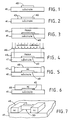
- Fig. 1 is a simplified cross-sectional view of an initial processing step in accordance with the present invention wherein a sacrificial layer is formed on a substrate.
- Fig. 2 shows the structure of Fig. 1 with the addition of a plating base.
- Fig. 3 shows the structure of Fig. 2 with the addition of a layer of PMMA photoresist.
- Fig. 4 shows the structure of Fig. 3 being exposed to X-rays through an X-ray mask.
- Fig. 5 shows the structure of Fig. 4 after developing and electroplating of nickel into the area of the developed PMMA.
- Fig. 6 shows the structure of Fig. 5 after removal of the PMMA.
- Fig. 7 is a perspective view of the remaining nickel structure on the substrate after removal of the PMMA and the sacrificial layer.
- Fig. 8 is a simplified perspective view of a micromechanical device having a rotating rotor which is driven by a magnet rotating beneath the substrate on which the rotor is mounted.
- Fig. 9 is a plan view of a micromechanical motor in accordance with the present invention formed on a substrate.
- Fig. 10 is a photomicrograph of a micromechanical motor of the type shown in Fig. 9.
- Fig. 11 is a perspective view of an exemplary magnetic field generator which can be coupled to the micromotor of Fig. 9 to drive the rotor of the same.
- Fig. 12 is a cross-sectional view of a first step in a process for the formation of a magnetic micromotor.
- Fig. 13 is a plan view of the structure shown in Fig. 12.
- Fig. 14 is a cross-sectional view of the structure of Fig. 12 after further step of processing.
- Fig. 15 is a plan view of the structure of Fig. 14.
- Fig. 16 is a cross-sectional view of the structure of Fig. 14 after further processing.
- Fig. 17 is a plan view of the structure of Fig. 16.
- Fig. 18 is a cross-sectional view of the structure of Fig. 16 after assembly of a rotor onto the structure.
- Fig. 19 is a plan view of the structure of Fig. 18.
- Fig. 20 is a cross-sectional view through a substrate illustrating a first step in another process for forming a magnetic micromotor.
- Fig. 21 is a plan view of the structure of Fig. 20.
- Fig. 22 is a cross-sectional view of the structure of Fig. 20 after a further step of processing.
- Fig. 23 is the plan view of the structure of Fig. 22.
- Fig. 24 is a cross-sectional view of the structure of Fig. 22 after further processing.
- Fig. 25 is a plan view of the structure of Fig. 24.
- Fig. 26 is a cross-sectional view of the structure of Fig. 24 after further processing.
- Fig. 27 is a plan view of the structure of Fig. 26.
- Fig. 28 is a cross-sectional view of the structure of Fig. 26 after further processing.
- Fig. 29 is a plan view of the structure of Fig. 28.
- Fig. 30 is a cross-sectional view of the structure of Fig. 28 after further processing.
- Fig. 31 is a plan view of the structure of Fig. 30.
- Fig. 32 is a cross-sectional view of the structure of Fig. 30 after further processing.
- Fig. 33 is a plan view of the structure of Fig. 32.
- Fig. 34 is a simplified perspective view, partially cut away, of the completed magnetic micromotor of the type illustrated in Figs. 32 and 33.
- Fig. 35 is a photomicrograph of another rotor and stator structure in accordance with the inventors.
- Fig. 36 is a photomicrograph of an assembled stepping motor in accordance with the invention.
- Fig. 37 is a photomicrograph of an assembled wobble motor in accordance with the invention.
- sacrificial layer LIGA process utilized in the present invention is illustrated in Figs. 1-7 and is described below with reference to these figures.
- LIGA processing involves maximum temperatures of 180°C or so. This property makes material selection for the sacrificial layer or layers quite easy because many material candidates exist. The requirements are simply that the sacrificial material can be applied with good adhesion, that it can be locally defined, and that it can be covered with a plating base without flank coverage problems. In addition, X-ray damage must be minimized and removal via surface micromachining or lateral etching must not modify the plated metal. Reasonable systems for plated nickel are polysilicon with hydrazine as an etch or various double metal combinations. A very convenient sacrificial layer is a spin coated polyimide film which remains soluble in bases for bake-out temperatures to 270°C or so.
- This film can be covered by a positive photoresist which enables pattern transfer from an optical mask to the photoresist. Since the developer for positive resist is basic, pattern transfer to the polyimide is achieved via dissolution in the exposed section of the substrate. A heat cycle follows which renders the polyimide mildly soluble in bases and therefore can be followed by a second or third sacrificial layer with a different polyimide thickness.
- a satisfactory plating base is a sputtered film which consists of 150 ⁇ of titanium followed by 150 ⁇ of nickel. This film cannot be patterned in normal situations because electronic contact to the plating fluid has to be established.
- the prepared substrate is next subjected to the basic LIGA procedure: thick PMMA photoresist application to form a layer 45 as shown in Fig. 3, exposure through an X-ray mask 46 as shown in Fig. 4, developing of the PMMA and electroplating to form the nickel part 48 as shown in Fig. 5.
- the X-ray mask is geometrically related to the patterned sacrificial layer and therefore must be aligned to the processed substrate.
- the alignment requirement is complicated by the fact that the exposure source is physically separate from the alignment tools.
- alignment is followed by the use of a clamping mechanism which can be removed from the alignment tool and allows transport and insertion into the X-ray source without mask to substrate slippage.
- the actual alignment can be accomplished by using optical techniques in a double-sided mask aligner which can accommodate the alignment-clamping fixture.
- Optical alignment becomes less complicated if the X-ray mask is totally or locally optically transparent. This can be accomplished more directly if the X-ray mask blank is formed from strain controlled silicon nitride.
- the absorber is a patterned layer of gold which is supplied by additive processing, e.g., by electroplating, and therefore has the desired edge acuity which is difficult to obtain with subtractive processing, e.g., etching, for absorber thicknesses near 4 microns.
- subtractive processing e.g., etching
- the processing continues with the removal of the used PMMA to leave the isolated structure 48 as shown in cross-section in Fig. 6. This can be accomplished by re-exposure and a second developing cycle or by suitable plasma etching.
- the unwanted sections of the plating base are removed by wet etching and the exposed sacrificial layer is dissolved in ammonium hydroxide to form the finished structure.
- this structure has a cavity 50 where the sacrificial layer 40 was located, and allows the structure 48 to be completely removed from the substrate 41 if the sacrificial layer is formed under the entire structure.
- the sacrificial layer LIGA process can be applied to create a variety of microstructures formed of metal which have previously been formed of silicon via silicon micromachining.
- the sacrificial layer LIGA process allows simpler processing with typical mask level reductions from six or eight to two, and very high aspect ratio structures which scale directly into higher force outputs for actuators.
- the process can be used with any planar substrate to which the sacrificial layer and the plating base can be attached. Therefore, typical silicon substrates are acceptable, but so are quartz, sapphire, glass, plastic, and metal substrates.
- Nickel and several of its alloys are ferromagnetic. They exhibit high permeabilities (low reluctance) for low flux densities and saturate at high magnetic fields of 10,000 gauss or so. At 3 micron working gaps and 1x10⁵ volt/cm electric fields, magnetic fields of 10,000 gauss produce roughly three orders of magnitude larger gap pressures than can be obtained with electrostatic fields.
- Magnetic fields are established by currents.
- the driving point impedance for single turn excitation conductors typically involves one or two ohms of DC resistance and inductance in the few nanohenry range. Current drive to 200 milliamperes will therefore involve voltage drops below a full volt. Bipolar rather than CMOS circuitry can achieve this easily and is nearly a perfect match for micromagnetics.
- FIG. 8 An exemplary magnetically actuated micro-device is illustrated in Fig. 8.
- a permanent magnet 55 mounted for rotation on the shaft 58 of a motor 58 is located beneath the backside of a substrate 59 and its field is coupled through stator poles 61 to a rotating rotor 62 on the substrate surface.
- Rotation of the magnet 55 beneath the stator, or equivalently, two phase excitation by an electromagnet of the stator produces a rotating magnetic field which drives rotation of the rotor 62.
- This field can be increased by bringing the magnetic excitation closer to the actuator.
- the minimum magnetic field which causes rotation can be measured by a suitable gauss meter.
- Such 100 micron structures are found to rotate quite satisfactorily at magnetic field strengths of 6 gauss or so. This is only about one order of magnitude above the earth's magnetic field.
- a basic magnetic micro-motor 98 is shown in plan view in Fig. 9, and Fig. 10 is a photomicrograph of the completed structure.
- the micromotor 98 is formed on a substrate 99 and has a rotor 100 rotatable about a post 101 which acts as the hub for the rotor.
- the motor includes two sets of stator pole pieces 102 and 103 arranged perpendicular to each other to allow two phase driving of the rotor 100.
- the rotor 100 has a peripheral ring with an outer surface with gear teeth 104 thereon which mesh with the teeth of a gear 105, and rotates about a shaft 106.
- a gear 108 rotating about a shaft 109 is engaged to the gear 105, and a gear 110 rotating about a shaft 111 is engaged to the gear 108.
- Power may thus be taken off the train of gears 105, 108, and 110 by other mechanical devices (not shown) to accomplish desired mechanical tasks.
- the rotor 100 can also be driven by applying a time varying magnetic field between the stator pole pieces 102 and 103.
- An example of an external device which can be utilized to couple a time varying magnetic flux to the stator pole pieces 102 and 103 is shown in Fig. 11.
- This structure utilizes two magnetic metal core pieces for providing a quadrature flux paths.
- the first core piece includes a U-shaped bar 115 of ferromagnetic material such as nickel which is engaged to quarter pieces 116 and 117, and a second U-shaped magnetic bar 120 which is engaged to quarter pieces 121 and 122.
- a first phase winding 124 is wound around the bar 115 and a second phase winding 126 is wound around the bar 120.
- the bars and quarter pieces function as flux guides and are also formed of ferromagnetic material such as nickel.
- the free ends of the quarter pieces 129-132 are adapted to engage with the top of the widened portions of the four stator pole structures 102 and 103 so that, for example, a current passed through the first phase winding 124 will provide a flux path between the stator pole pieces 102 through the rotor, whereas current passed through the coil 126 will provide a magnetic flux path between the stator pole pieces 103 through the rotor 100.
- a current passed through the first phase winding 124 will provide a flux path between the stator pole pieces 102 through the rotor
- current passed through the coil 126 will provide a magnetic flux path between the stator pole pieces 103 through the rotor 100.
- the rotor may be one which is permanently magnetized along its way (low reluctance) axis. This will increase the maximum torque which can be produced.
- the rotor material should be preferably be magnetically bard (i.e., have a square B-H loop) with high coercivity. This may be accomplished be electroplating an alloy of nickel with high coercivity (e.g., nickel-cobalt) and by using approximate anneal cycles.
- the electroplated part may be magnetized during electroplating or after release from the substrate in a sufficiently intense magnetic field.
- the rotor may be non-solvent (have no variation in reluctance along any direction of its axis) and have torque generated by the alternating or rotating hysteresis losses which will occur when the rotor is subjected to a rotating magnetic field.
- Fig. 35 shows an alternative rotor construction in which the rotor has multiple poles formed as spokes or gear teeth, and thus has multiple low and high reluctance paths therethrough.
- Fig. 36 shows another spoke-like rotor construction which can be operated as a stepping motor.
- Fig. 37 shows a round rotor having an internal opening larger than the hub so that the rotor rotates eccentrically and functions as a wobble rotor.
- a plating base of titanium (about 150 Angstroms) and nickel (about 150 Angstroms) is sputtered onto a substrate 130, which may be of any relatively, flat, polished, clean material, such as single crystal silicon, quartz, sapphire, glass, or comparable substrate materials.
- Linear PMMA is then spun onto the plating base 131 to a thickness of about 6 ⁇ m and the PMMA is then patterned optically (X-ray lithography is not necessary because of the relatively thin layer of PMMA which is being patterned) and nickel is electroplated to about 5 ⁇ m.
- the polyimide isolation layer is then spun on to roughly 3 ⁇ m thickness and soft annealed.
- the isolation layer is then patterned to open up stator anchors and contacts to current carrying lines, and a plating base of titanium and nickel is described as before is then sputtered onto the overall structure.
- the structure at this point is illustrated in cross-section in Fig. 14, and in elevation in Fig. 15, in which the polyimide isolation layer 138 overlays the other structures except for openings 140 for stator contacts and openings 141 for conductive wire connections to the stator electrical conductors.
- PMMA is then cast to the desired thickness of the major structures, e.g., 100 microns or more, and the X-ray mask is then aligned to the PMMA which defines the stator, hub and winding leads.
- Synchrotron X-ray exposure is then carried out, with developing of the PMMA to leave the desired cavities, and then nickel is electroplated to the desired thickness.
- the remaining PMMA is then removed, leaving structures as illustrated in cross-section in Fig. 16 and in plan view in Fig. 17. These include stator pole pieces 150 for a first phase and pole pieces 152 for a second phase, formed of the electroplated nickel, which are mounted to the substrate by contact with the plating base at the exposed portions of the magnetic flux return ring 133, and a central hub 153.
- Both of these structures are relatively high, e.g., in the range of a 100 ⁇ m.
- the polyimide release layer 138 is left extending outwardly from the stator pole pieces 150 and 152 to an inner peripheral wall 156.
- Current contacts 154 and 155 are formed of nickel for proving a current path connection to the conductors 134 and 135 which underlie the stator pieces 150 and 152.
- the final step is the addition of a rotor 160 which fits over the hub 153 between the pole pieces 150 and 152 and which is supported at its edges for rotation by a portion of the polyimide isolation layer 138.
- Illustrative electrical connections for the phase windings include a first wire 164 for the first phase which connects to one of the pole conductors 154, with the circuit being completed from the other end of the pole conductor through a conductor 165 to the diametrically opposite pole conductor 154, and from the other pole conductor through an electrical lead 166.
- the second phase connections are provided by a wire 168 connected to one of the conductors 155 for the second phase, from the other end of the conductor 155 by a wire 169 to the diametrically opposite phase conductor 155, and thence completed from the other phase conductor through a wire 170.
- isolation layer contact areas are defined.
- the current windings could be plated from copper on both the first and third layers by separating the stator and wire patterns into individual masks, and repeating the first and third layer processing using copper (or gold, or any high conducting, non-magnetic electroplated metal). Using nickel for the windings will not result in a substantive change in the performance of the device, although it does have higher resistivity than either copper or gold.
- a plating base is sputtered onto a starting substrate, for example, glass, and comprises a layer of titanium (about 150 Angstroms) and nickel (about 150 Angstroms) to provide a plating base 201 on the top surface of the substrate 200.
- Linear PMMA is then spun on in a layer with a thickness of about 6 ⁇ m.
- the PMMA is patterned optically and nickel is electroplated to about 5 ⁇ m to form the nickel base layer.
- the PMMA and the plating base is then removed to leave a nickel flux return path 202 in a ring with a center opening 204.
- a first polyimide (PiRL) layer is spun on roughly to 3 ⁇ m thickness and soft annealed to form the layer 208.
- Aluminum is then sputtered on to about 4 ⁇ m and windings are patterned with a P-A-N etch to form the windings 210 which have a general U-shaped with a center bridge section 211.
- a second PiRL isolation layer 214 is then spun on to about 3 microns and soft annealed.
- vias are then etched in the PiRL for stator anchoring and rotary etch supports, and the remaining PiRL is hard annealed (at about 300° C). This leaves openings 216 and 217 in the PiRL and an inner wall 219 which surrounds the open area 204. Note that the conductive layer 211 is encased within the PiRL layers 208 and 214.
- a third layer of PiRL is spun on for contact protection in the areas 221 to about 2 ⁇ m and soft annealed.
- the protection layer is then patterned leaving the PiRL only over the contacts in the areas 221 and a plating base 222 of titanium and nickel is then sputtered on.
- PMMA is then cast onto the structure, an X-ray mask containing stator and hub definition is then aligned to the structure and the synchrotron X-ray exposure is made. After removal of the PMMA the exposed areas, nickel is electro-plated in and the entire remaining PMMA is exposed to synchrotron X-rays and developed to remove the PMMA, leaving the stator structures 223 in the central hub 224.
- the plating base is then removed, the PiRL contact protection layer is removed, and the contact wires 230 are then bonded to the exposed areas of the conductors 210 to complete the circuit.
- the rotor 235 constructed separately on another substrate using the sacrificial layer technique shown in Figs. 1-7, is then assembled onto the hub 224.
- the rotor preferably has a central bar section 236 which provides a low reluctance a flux path between the stator pole pieces 223 and a thinner peripheral ring section 237 which, with the openings 236, defines a high reluctance path perpendicular to the low reluctance path.
- the openings which accepts the hub is formed in the center bar.
- the fully assembled motor is also shown in simplified perspective view in Fig. 34.
- the magnetic flux path is patterned to provide the return path for the stator.
- the first step corresponds to steps 1-7 in the integrated processing sequence described above.
- Pattern openings in PiRL layer for stator pole contacts underlying flux path layer and contacts to aluminum windings, as well as standoffs for the rotor.
- Assemble rotor onto center post The rotor is fabricated on a separate substrate and released via an unpatterned PiRL sacrificial layer which underlies the entire rotor structure.
- the rotor may have gear teeth defined on its perimeter as shown above for driving external gears between the stator poles and, in turn, a mechanical system.
Abstract
Description
- This invention pertains generally to the field of semiconductor and micromechanical devices and processing techniques therefor, and particularly to microminiature magnetic devices.
- Deep X-ray lithography involves a substrate which is covered by thick photoresist, typically severally hundred microns in thickness, which is exposed through a mask by X-rays. X-ray photons are much more energetic than optical photons, which makes complete exposure of thick photoresist films feasible and practical. Furthermore, since X-ray photons are short wavelength particles, diffraction effects which typically limit device dimensions to two or three wavelengths of the exposing radiation are absent for mask dimensions above 0.1 micron. If one adds to this the fact that X-ray photons are absorbed by atomic processes, standing wave problems, which typically limit exposures of thick photoresist by optical means, become an non-issue for X-ray exposures. The use of a synchrotron for the X-ray source yields high flux densities--several watts per square centimeter--combined with excellent collimation to produce thick photoresist exposures without any horizontal run-out. Locally exposed patterns should therefore produce vertical photoresist walls if a developing system with very high selectivity between exposed and unexposed photoresist is available. This requirement is satisfied for polymethylmethacrylate (PMMA) as the X-ray photoresist and an aqueous developing system. See, H. Guckel, et al., "Deep X-Ray and UV Lithographies For Micromechanics", Technical Digest, Solid State Sensor and Actuator Workshop, Hilton Head, S.C., June 4-7, 1990, pp. 118-122.
- Deep X-ray lithography may be combined with electroplating to form high aspect ratio structures. This requires that the substrate be furnished with a suitable plating base prior to photoresist application. Typically this involves a sputtered film of adhesive metal such as chromium or titanium which is followed by a thin film of the metal which is to be plated. Exposure through a suitable mask and development are followed by electroplating. This results, after cleanup, in fully attached metal structures with very high aspect ratios. Such structures were first reported by W. Ehrfeld and co-workers at the Institute for Nuclear Physics at the University of harlsruhe in West Germany. Ehrfeld termed the process "LIGA" based on the first letters of the German words for lithography and electro-plating. A general review of the LIGA process is given in the article by W. Ehrfeld, et al., "LIGA Process: Sensor Construction Techniques Via X-Ray Lithography", technical Digest, IEEE Solid-State Sensor and Actuator Workshop, 1988, pp. 1-4.
- A difficulty with the original LIGA process is that it can only produce fully attached metal structures. This restricts the possible application areas severely and unnecessarily.
- The addition of a sacrificial layer to the LIGA process facilitates the fabrication of fully attached, partially attached, or completely free metal structures. Because device thicknesses are typically larger than 10 microns and smaller than 300 microns, freestanding structures will not distort geometrically if reasonable strain control for the plated film is achieved. This fact makes assembly in micromechanics possible and thereby leads to nearly arbitrary three-dimensional structures. See H. Guckel, et al., "Fabrication of Assembled Micromechanical Components via Deep X-Ray Lithography," Proceedings of IEEE Micro Electro Mechanical Systems, January 30 - February 2, 1991, pp. 74-79.
- In accordance with the present invention, micromechanical devices are formed on a substrate utilizing a sacrificial layer deep X-ray lithography process to produce a rotating micropart or rotor which is driven magnetically. The rotor, which typically will have a diameter of a few hundred microns or less, is formed as a free structure which is assembled onto a hub formed on the substrate. The rotor may be formed to have low-reluctance and high-reluctance paths through it. Surrounding the rotor on the substrate are stator pole pieces which are structured to channel magnetic flux to the rotor. Both the rotor and the stator pole pieces are formed of a ferromagnetic material, such as nickel, which is well suited to providing a magnetic flux path.
- The stator pole pieces form part of a means for providing a rotating magnetic field in the region of the rotor. The rotating magnetic field can be provided, for example, by a rotating magnet beneath the substrate on which the rotor is mounted, or by an external magnet which couples a magnetic flux to the stator pole pieces in a time varying manner to create the rotating magnetic field. In a preferred embodiment, the electrical excitation to provide the magnetic field in the pole pieces is provided by conductors formed integrally on the substrate with the stator pole pieces. Such conductors may be formed as conductive strips surrounding upstanding stator pole pieces or as adjacent conductors formed on the substrate which provide a current which encircles the pole piece to induce a magnetic flux therein By providing perpendicular pairs of pole pieces, each excited by sinusoidal currents, 90° out of phase with the other, rotating magnetic fields can be generated in the rotor region which will drive the rotor to rotate with the magnetic field.
- Utilization of a sacrificial layer in conjunction with the LIGA process allows the rotor to be formed of a ferromagnetic metal such as nickel at substantial vertical dimensions, e.g., a hundred microns or more, which allows formation of stable structures which can be handled and assembled into place. Additional gears can also be formed by the sacrificial layer process which can be engaged to the rotor, such as by having gear teeth on the periphery of the rotor engage the gear teeth of the gears. The gears can thereby be utilized to provide power transfer to other mechanically driven devices.
- Further objects, features and advantages of the invention will be apparent from the following detailed description when taken in conjunction with the accompanying drawings.
- In the drawings:
- Fig. 1 is a simplified cross-sectional view of an initial processing step in accordance with the present invention wherein a sacrificial layer is formed on a substrate.
- Fig. 2 shows the structure of Fig. 1 with the addition of a plating base.
- Fig. 3 shows the structure of Fig. 2 with the addition of a layer of PMMA photoresist.
- Fig. 4 shows the structure of Fig. 3 being exposed to X-rays through an X-ray mask.
- Fig. 5 shows the structure of Fig. 4 after developing and electroplating of nickel into the area of the developed PMMA.
- Fig. 6 shows the structure of Fig. 5 after removal of the PMMA.
- Fig. 7 is a perspective view of the remaining nickel structure on the substrate after removal of the PMMA and the sacrificial layer.
- Fig. 8 is a simplified perspective view of a micromechanical device having a rotating rotor which is driven by a magnet rotating beneath the substrate on which the rotor is mounted.
- Fig. 9 is a plan view of a micromechanical motor in accordance with the present invention formed on a substrate.
- Fig. 10 is a photomicrograph of a micromechanical motor of the type shown in Fig. 9.
- Fig. 11 is a perspective view of an exemplary magnetic field generator which can be coupled to the micromotor of Fig. 9 to drive the rotor of the same.
- Fig. 12 is a cross-sectional view of a first step in a process for the formation of a magnetic micromotor.
- Fig. 13 is a plan view of the structure shown in Fig. 12.
- Fig. 14 is a cross-sectional view of the structure of Fig. 12 after further step of processing.
- Fig. 15 is a plan view of the structure of Fig. 14.
- Fig. 16 is a cross-sectional view of the structure of Fig. 14 after further processing.
- Fig. 17 is a plan view of the structure of Fig. 16.
- Fig. 18 is a cross-sectional view of the structure of Fig. 16 after assembly of a rotor onto the structure.
- Fig. 19 is a plan view of the structure of Fig. 18.
- Fig. 20 is a cross-sectional view through a substrate illustrating a first step in another process for forming a magnetic micromotor.
- Fig. 21 is a plan view of the structure of Fig. 20.
- Fig. 22 is a cross-sectional view of the structure of Fig. 20 after a further step of processing.
- Fig. 23 is the plan view of the structure of Fig. 22.
- Fig. 24 is a cross-sectional view of the structure of Fig. 22 after further processing.
- Fig. 25 is a plan view of the structure of Fig. 24.
- Fig. 26 is a cross-sectional view of the structure of Fig. 24 after further processing.
- Fig. 27 is a plan view of the structure of Fig. 26.
- Fig. 28 is a cross-sectional view of the structure of Fig. 26 after further processing.
- Fig. 29 is a plan view of the structure of Fig. 28.
- Fig. 30 is a cross-sectional view of the structure of Fig. 28 after further processing.
- Fig. 31 is a plan view of the structure of Fig. 30.
- Fig. 32 is a cross-sectional view of the structure of Fig. 30 after further processing.
- Fig. 33 is a plan view of the structure of Fig. 32.
- Fig. 34 is a simplified perspective view, partially cut away, of the completed magnetic micromotor of the type illustrated in Figs. 32 and 33.
- Fig. 35 is a photomicrograph of another rotor and stator structure in accordance with the inventors.
- Fig. 36 is a photomicrograph of an assembled stepping motor in accordance with the invention.
- Fig. 37 is a photomicrograph of an assembled wobble motor in accordance with the invention.
- The sacrificial layer LIGA process utilized in the present invention is illustrated in Figs. 1-7 and is described below with reference to these figures.
- LIGA processing involves maximum temperatures of 180°C or so. This property makes material selection for the sacrificial layer or layers quite easy because many material candidates exist. The requirements are simply that the sacrificial material can be applied with good adhesion, that it can be locally defined, and that it can be covered with a plating base without flank coverage problems. In addition, X-ray damage must be minimized and removal via surface micromachining or lateral etching must not modify the plated metal. Reasonable systems for plated nickel are polysilicon with hydrazine as an etch or various double metal combinations. A very convenient sacrificial layer is a spin coated polyimide film which remains soluble in bases for bake-out temperatures to 270°C or so. This film can be covered by a positive photoresist which enables pattern transfer from an optical mask to the photoresist. Since the developer for positive resist is basic, pattern transfer to the polyimide is achieved via dissolution in the exposed section of the substrate. A heat cycle follows which renders the polyimide mildly soluble in bases and therefore can be followed by a second or third sacrificial layer with a different polyimide thickness.
- The patterned sacrificial layer, shown at 40 in Fig. 1 on the top surface of a
substrate 41, is covered by theplating base 43 as shown in Fig. 2. Where nickel is to be plated, a satisfactory plating base is a sputtered film which consists of 150Å of titanium followed by 150Å of nickel. This film cannot be patterned in normal situations because electronic contact to the plating fluid has to be established. The prepared substrate is next subjected to the basic LIGA procedure: thick PMMA photoresist application to form alayer 45 as shown in Fig. 3, exposure through anX-ray mask 46 as shown in Fig. 4, developing of the PMMA and electroplating to form thenickel part 48 as shown in Fig. 5. However, there is a severe technical problem: the X-ray mask is geometrically related to the patterned sacrificial layer and therefore must be aligned to the processed substrate. The alignment requirement is complicated by the fact that the exposure source is physically separate from the alignment tools. In a preferred procedure, alignment is followed by the use of a clamping mechanism which can be removed from the alignment tool and allows transport and insertion into the X-ray source without mask to substrate slippage. The actual alignment can be accomplished by using optical techniques in a double-sided mask aligner which can accommodate the alignment-clamping fixture. Optical alignment becomes less complicated if the X-ray mask is totally or locally optically transparent. This can be accomplished more directly if the X-ray mask blank is formed from strain controlled silicon nitride. The absorber is a patterned layer of gold which is supplied by additive processing, e.g., by electroplating, and therefore has the desired edge acuity which is difficult to obtain with subtractive processing, e.g., etching, for absorber thicknesses near 4 microns. Mask blanks made from other materials, such as fine grained polysilicon, can also be used but must have locally transparent regions for the present alignment scheme which leads to more complicated mask fabrication procedures. - The processing continues with the removal of the used PMMA to leave the
isolated structure 48 as shown in cross-section in Fig. 6. This can be accomplished by re-exposure and a second developing cycle or by suitable plasma etching. The unwanted sections of the plating base are removed by wet etching and the exposed sacrificial layer is dissolved in ammonium hydroxide to form the finished structure. As illustrated in Fig. 7, this structure has acavity 50 where thesacrificial layer 40 was located, and allows thestructure 48 to be completely removed from thesubstrate 41 if the sacrificial layer is formed under the entire structure. - The sacrificial layer LIGA process can be applied to create a variety of microstructures formed of metal which have previously been formed of silicon via silicon micromachining. Generally, the sacrificial layer LIGA process allows simpler processing with typical mask level reductions from six or eight to two, and very high aspect ratio structures which scale directly into higher force outputs for actuators. Moreover the process can be used with any planar substrate to which the sacrificial layer and the plating base can be attached. Therefore, typical silicon substrates are acceptable, but so are quartz, sapphire, glass, plastic, and metal substrates.
- Nickel and several of its alloys are ferromagnetic. They exhibit high permeabilities (low reluctance) for low flux densities and saturate at high magnetic fields of 10,000 gauss or so. At 3 micron working gaps and 1x10⁵ volt/cm electric fields, magnetic fields of 10,000 gauss produce roughly three orders of magnitude larger gap pressures than can be obtained with electrostatic fields.
- Magnetic fields are established by currents. The driving point impedance for single turn excitation conductors typically involves one or two ohms of DC resistance and inductance in the few nanohenry range. Current drive to 200 milliamperes will therefore involve voltage drops below a full volt. Bipolar rather than CMOS circuitry can achieve this easily and is nearly a perfect match for micromagnetics.
- An exemplary magnetically actuated micro-device is illustrated in Fig. 8. A
permanent magnet 55 mounted for rotation on theshaft 58 of amotor 58 is located beneath the backside of asubstrate 59 and its field is coupled throughstator poles 61 to arotating rotor 62 on the substrate surface. Rotation of themagnet 55 beneath the stator, or equivalently, two phase excitation by an electromagnet of the stator, produces a rotating magnetic field which drives rotation of therotor 62. This field can be increased by bringing the magnetic excitation closer to the actuator. Most importantly, the minimum magnetic field which causes rotation can be measured by a suitable gauss meter. Such 100 micron structures are found to rotate quite satisfactorily at magnetic field strengths of 6 gauss or so. This is only about one order of magnitude above the earth's magnetic field. - A basic magnetic micro-motor 98 is shown in plan view in Fig. 9, and Fig. 10 is a photomicrograph of the completed structure. The micromotor 98 is formed on a
substrate 99 and has arotor 100 rotatable about apost 101 which acts as the hub for the rotor. The motor includes two sets ofstator pole pieces rotor 100. Therotor 100 has a peripheral ring with an outer surface withgear teeth 104 thereon which mesh with the teeth of agear 105, and rotates about ashaft 106. Agear 108 rotating about ashaft 109 is engaged to thegear 105, and agear 110 rotating about ashaft 111 is engaged to thegear 108. Power may thus be taken off the train ofgears - In addition to being driven by an external rotating magnet, the
rotor 100 can also be driven by applying a time varying magnetic field between thestator pole pieces stator pole pieces U-shaped bar 115 of ferromagnetic material such as nickel which is engaged toquarter pieces magnetic bar 120 which is engaged toquarter pieces bar 115 and a second phase winding 126 is wound around thebar 120. Extending from the bottom of thequarter pieces quarter pieces quarter pieces quarter pieces stator pole structures stator pole pieces 102 through the rotor, whereas current passed through thecoil 126 will provide a magnetic flux path between thestator pole pieces 103 through therotor 100. By providing sinusoidally varying currents to the twocoils - The rotor may be one which is permanently magnetized along its way (low reluctance) axis. This will increase the maximum torque which can be produced. In such a case, the rotor material should be preferably be magnetically bard (i.e., have a square B-H loop) with high coercivity. This may be accomplished be electroplating an alloy of nickel with high coercivity (e.g., nickel-cobalt) and by using approximate anneal cycles. The electroplated part may be magnetized during electroplating or after release from the substrate in a sufficiently intense magnetic field.
- Since ferromagnetic materials like nickel exhibit hysteresis, the rotor may be non-solvent (have no variation in reluctance along any direction of its axis) and have torque generated by the alternating or rotating hysteresis losses which will occur when the rotor is subjected to a rotating magnetic field.
- Fig. 35 shows an alternative rotor construction in which the rotor has multiple poles formed as spokes or gear teeth, and thus has multiple low and high reluctance paths therethrough. Fig. 36 shows another spoke-like rotor construction which can be operated as a stepping motor. Fig. 37 shows a round rotor having an internal opening larger than the hub so that the rotor rotates eccentrically and functions as a wobble rotor.
- The construction of a motor in which the electrical excitation is integrated on the substrate with the stator is shown in Figs. 12-19. With reference to these figures, the construction can be bristly described as follows. First, a plating base of titanium (about 150 Angstroms) and nickel (about 150 Angstroms) is sputtered onto a
substrate 130, which may be of any relatively, flat, polished, clean material, such as single crystal silicon, quartz, sapphire, glass, or comparable substrate materials. Linear PMMA is then spun onto theplating base 131 to a thickness of about 6µm and the PMMA is then patterned optically (X-ray lithography is not necessary because of the relatively thin layer of PMMA which is being patterned) and nickel is electroplated to about 5µm. The PMMA and the plating base in the areas other than underneath the nickel is then removed. This leaves the structure as shown in cross-section in Fig. 12, and in plan view in Fig. 13, in which there is a ring shaped magneticflux return path 133 formed of nickel and fournickel pads - The polyimide isolation layer is then spun on to roughly 3µm thickness and soft annealed. The isolation layer is then patterned to open up stator anchors and contacts to current carrying lines, and a plating base of titanium and nickel is described as before is then sputtered onto the overall structure. The structure at this point is illustrated in cross-section in Fig. 14, and in elevation in Fig. 15, in which the
polyimide isolation layer 138 overlays the other structures except foropenings 140 for stator contacts andopenings 141 for conductive wire connections to the stator electrical conductors. - PMMA is then cast to the desired thickness of the major structures, e.g., 100 microns or more, and the X-ray mask is then aligned to the PMMA which defines the stator, hub and winding leads. Synchrotron X-ray exposure is then carried out, with developing of the PMMA to leave the desired cavities, and then nickel is electroplated to the desired thickness. The remaining PMMA is then removed, leaving structures as illustrated in cross-section in Fig. 16 and in plan view in Fig. 17. These include
stator pole pieces 150 for a first phase andpole pieces 152 for a second phase, formed of the electroplated nickel, which are mounted to the substrate by contact with the plating base at the exposed portions of the magneticflux return ring 133, and acentral hub 153. Both of these structures are relatively high, e.g., in the range of a 100 µm. Note that thepolyimide release layer 138 is left extending outwardly from thestator pole pieces peripheral wall 156.Current contacts conductors stator pieces - The final step, as shown in Figs. 18 and 19, is the addition of a
rotor 160 which fits over thehub 153 between thepole pieces polyimide isolation layer 138. Illustrative electrical connections for the phase windings include afirst wire 164 for the first phase which connects to one of thepole conductors 154, with the circuit being completed from the other end of the pole conductor through a conductor 165 to the diametricallyopposite pole conductor 154, and from the other pole conductor through an electrical lead 166. The second phase connections are provided by awire 168 connected to one of theconductors 155 for the second phase, from the other end of theconductor 155 by awire 169 to the diametricallyopposite phase conductor 155, and thence completed from the other phase conductor through awire 170. By applying sinusoidally varying electrical currents to thefirst phase wires 164, 166 and to thesecond phase wire - The following describes the processing steps for carrying out the construction of the motor structure described above.
- Define inter-stator magnetic flux paths and returns for current carrying wires.
- 1. A plating base of 150 Angstroms of titanium followed by 150 Angstroms of Nickel is sputtered onto the substrate material. This initial step defines the first layer which provides the inter-stator magnetic flux paths and the returns for the current carrying wires.
- 2. Spin on linear PMMA (KTI PMMA 9% solids, dyed with coumarin 6 in the ratio 25 ml PMMA to 50 mg coumarin 6) to a thickness of 6 µm using an anneal sequence of: 60°C/hr. ramped up to 180° C, hold for one hour, 60° C/hr. ramp down to room temperature, for each layer of PMMA (4 layers of PMMA are necessary at 1.5 µm each when spun at 2 krpm for 30 seconds).
- 3. Pattern PMMA with a 2-layer photo resist process.
- a) Spin KTI 809 PR on PMMA at 5 krpm,
- b) Prebake at 90° C for 15 minutes,
- c) Expose the layer of 809 with first layer mask and develop in 1:1 809 developer:water,
- d) Blanket deep UV (230 nm) expose PMMA,
- e) Develop in the following 3 baths for:
Five minutes in:
60% vol. 2-(2-butoxy ethoxy) ethanol
20% vol. Tetrahydro-1-4 oxizin (morpholine)
5% vol. 2-aminoethanol (ethanolamine)
15% vol. distilled, deionized water;
Twenty minutes in:
80% vol. 2-(2-butxoyethoxy) ethanol
20% vol. water.
Then five minutes in:
100% water. (All baths are held at 35.0° C + or - 0.5° C).
- 4. Preparation for electro-plating:
- a) O₂ plasma descum for 2 minutes. (In Plasma Therm 1440, for example: O₂= 25 SCCM, pressure = 30 mT,power = 50 watts).
- b) Treat nickel plating base with 5% HCl for 15 minutes.
- 5. Electroplate nickel to 5 µm thickness at 50 mΛ/cm² in a nickel sulfamate plating bath.
- 6. Remove PMMA by blanket deep UV exposure and a development cycle as in 3(e) above.
- 7. Remove plating base:
Ni 40 minutes in 5% HCl, 5 minute water rinse; Ti, 2 minutes in 200:1 HF (49% HF), 15 minute water rinse. - Define isolation layer contact areas.
- 8. Spin on PiRL(I) (polyimide release layer from Brewer Science, Rolla, Mo.) to a thickness of 3 µm and bake at 210° for one minute on a hot plate.
- 9. Pattern PiRL to open up plating areas for current wires and stator flux paths:
- a) spin Shipley 1400-27 PR on PiRL,
- b) align and pattern contacts to flux paths and current wires in 1400-27 PR layer which carries over to PiRL layer (MF-321 Shipley developer may be used),
- c) remove 1400-27 PR using acetone,
- d) descum with O₂ plasma for one minute as in 4(a) above.
- e) the PiRL at this point may be hard baked between 300°C and 350°C if it will not be removed at the end of the process (step 19 below).
- 10. Sputter 150 Angstroms Ti followed by 150 Angstroms Ni.
-
- Deep X-ray lithography defined layer.
- 11. Cast PMMA typically to about 100-200 µm.
- 12. Align x-ray mask containing wire definitions and stator definitions to PiRL contact openings.
- 13. Synchrotron radiation expose the cast PMMA to a dose of 3.5 kJ/cm³ at the bottom of the cast PMMA at 1 Gev beam energy (e.g., such as provided by the Aladin Synchrotron, Stoughton, Wisconsin).
- 14. Develop using the same sequence as in 3(e) above wherein the times are about 20 minutes in the first bath, 20 minutes in the second bath, and 5 minutes in the third bath.
- 15. Prepare the substrate for nickel plating:
- a) O₂ plasma descum as in 4(a) above in 15 seconds on/45 seconds off intervals for a total on-time of 2 minutes,
- b) 5% HCl cut for 15 minutes.
- 16. Nickel electroplate at 50 mΛ/cm² in nickel sulfamate bath (plating rate is about 1µm/minute).
- 17. Remove cast PMMA via second synchrotron blanket X-ray exposure and development as in
Step 14 above. - Assemble rotor on center hub, the rotor having been processed on a separate substrate and released via an unpatterned PiRL sacrificial layer.
- 18. Remove plating base:
Ni, 40 minutes in 5% HCl 5 minutes of water rinse,
Ti: 2 minutes in 200:1 HF(49%), 15 minutes of water rinse. - 19. (Optional): The PiRL layer may be removed with a suitable basic solution (for example, in 3:1 H₂O:NH₄OH).
- 20. Bond out wiring to the individual stators (may be soldered or silver epoxied to nickel windings).
- 21. Assemble the corresponding rotor on the center post.
- It is noted that the current windings could be plated from copper on both the first and third layers by separating the stator and wire patterns into individual masks, and repeating the first and third layer processing using copper (or gold, or any high conducting, non-magnetic electroplated metal). Using nickel for the windings will not result in a substantive change in the performance of the device, although it does have higher resistivity than either copper or gold.
- The formation of an alternative electrical excitation system for a magnetic micromotor is shown in Figs. 20-33, and forms the motor structure shown in perspective view in Fig. 34. The basic process can be summarized with reference to these figures, starting with Figs. 20 and 21. First, a plating base is sputtered onto a starting substrate, for example, glass, and comprises a layer of titanium (about 150 Angstroms) and nickel (about 150 Angstroms) to provide a
plating base 201 on the top surface of thesubstrate 200. Linear PMMA is then spun on in a layer with a thickness of about 6 µm. The PMMA is patterned optically and nickel is electroplated to about 5 µm to form the nickel base layer. The PMMA and the plating base is then removed to leave a nickelflux return path 202 in a ring with acenter opening 204. - With respect to Figs. 22 and 23, a first polyimide (PiRL) layer is spun on roughly to 3 µm thickness and soft annealed to form the
layer 208. Aluminum is then sputtered on to about 4 µm and windings are patterned with a P-A-N etch to form thewindings 210 which have a general U-shaped with acenter bridge section 211. - With reference to Figs. 24 and 25, a second
PiRL isolation layer 214 is then spun on to about 3 microns and soft annealed. - As shown in Figs. 16 and 27, vias are then etched in the PiRL for stator anchoring and rotary etch supports, and the remaining PiRL is hard annealed (at about 300° C). This leaves
openings inner wall 219 which surrounds theopen area 204. Note that theconductive layer 211 is encased within the PiRL layers 208 and 214. - With reference to Figs. 28 and 29, a third layer of PiRL is spun on for contact protection in the
areas 221 to about 2 µm and soft annealed. The protection layer is then patterned leaving the PiRL only over the contacts in theareas 221 and aplating base 222 of titanium and nickel is then sputtered on. - With reference to Figs. 30 and 31, PMMA is then cast onto the structure, an X-ray mask containing stator and hub definition is then aligned to the structure and the synchrotron X-ray exposure is made. After removal of the PMMA the exposed areas, nickel is electro-plated in and the entire remaining PMMA is exposed to synchrotron X-rays and developed to remove the PMMA, leaving the
stator structures 223 in thecentral hub 224. - With reference to Figs. 32 and 33, the plating base is then removed, the PiRL contact protection layer is removed, and the
contact wires 230 are then bonded to the exposed areas of theconductors 210 to complete the circuit. Therotor 235, constructed separately on another substrate using the sacrificial layer technique shown in Figs. 1-7, is then assembled onto thehub 224. As is illustrated in Fig. 33, the rotor preferably has acentral bar section 236 which provides a low reluctance a flux path between thestator pole pieces 223 and a thinnerperipheral ring section 237 which, with theopenings 236, defines a high reluctance path perpendicular to the low reluctance path. The openings which accepts the hub is formed in the center bar. The fully assembled motor is also shown in simplified perspective view in Fig. 34. - The processing steps are described in more detail as follows:
- The magnetic flux path is patterned to provide the return path for the stator.
- The first step corresponds to steps 1-7 in the integrated processing sequence described above.
-
- 1. Pattern aluminum winding layer.
- 2. Spin-on PiRL to 3µm and bake at 210°C for one minute on a hot plate.
- 3. Sputter four µm of aluminum.
- 4. Pattern the aluminum using a standard wet-edge process, for example, use 1375 Shipley photoresist, align winding layer to underlying nickel flux path layer, etch aluminum in standard phosphoric-acetic-nitric acid aluminum etch solution, and remove photoresist with commercial PR stripper, (e.g., Shipley 1165).
- 5. Spin-on second PiRL layer (3µm thick) and bake at 210°C for one minute on a hot plate.
- Pattern openings in PiRL layer for stator pole contacts underlying flux path layer and contacts to aluminum windings, as well as standoffs for the rotor.
- 6. Use the same processing sequence as in step 9 of the previous integrated stator winding process.
- 7. Bake the PiRL layer to 300°C on a hot plate to hard anneal, making it non-developable in PMMA developer.
- 8. Sputter 150 Angstroms Ti and 150 Angstroms Ni plating base.
-
- 9. Spin third PiRL layer (about 2µm) and pattern over the aluminum contact areas as in step 6 above.
- Deep X-ray lithography layer for stator definition.
- 10. Use the same processing steps as in steps 11-17 of the first integrated winding process.
- 11. Remove the plating base as in
step 18 of the prior integrated stator winding process. - 12. Remove PiRL contact protection layer with 3:1 H₂O:NH₄OH.
- 13. Bond out aluminum current carrying wires using standard gold wire bonding.
- Assemble rotor onto center post. The rotor is fabricated on a separate substrate and released via an unpatterned PiRL sacrificial layer which underlies the entire rotor structure.
- It may be noted that the rotor may have gear teeth defined on its perimeter as shown above for driving external gears between the stator poles and, in turn, a mechanical system.
- It is understood that the invention is not confirmed to the embodiments set forth herein as illustrative, but embraces such forms thereof as come within the scope of the following claims.
Claims (21)
- A micromechanical magnetically actuated device comprising:(a) a rotor having a circular periphery with a diameter less than about 200 µm and formed of a ferromagnetic material, a substrate, and means for mounting the rotor for rotation on the substrate, the rotor formed to have a high reluctance path therethrough and a low reluctance path therethrough;(b) a stator having pole pieces formed of ferromagnetic material mounted on the substrate around the rotor for directing magnetic flux to the rotor and means for providing a time varying magnetic flux through the pole pieces to the rotor which rotates about the axis of rotation of the rotor.
- The device of Claim 1 wherein the means for providing the time varying magnetic flux includes an external electromagnet having two coils mounted around flux guides which extend to the stator pole pieces to provide flux to the stator pole pieces on opposite sides of the rotor region, the stator pole pieces being formed in pairs which are arranged perpendicular to one another about the rotor.
- The device of Claim 1 wherein the rotor pole pieces are formed as two pairs of pole pieces arranged perpendicularly to one another about the rotor, and wherein the means for providing a time varying flux includes a conductor formed around each of the pole pieces to induce a magnetic field therein when current is passed through the conductor, wherein the stator also includes a flux return path structure on the substrate formed of a ferromagnetic material which connects the stator pole pieces to provide a flux return path therethrough so that a complete path can be formed between opposite pairs of stator pole pieces through the rotor.
- The device of Claim 1 wherein the stator pole pieces are deposited by electroplating metal onto the substrate to a depth of at least 50µm.
- The device of Claim 1 wherein the rotor and the stator pole pieces are formed of electro-plated nickel.
- The device of Claim 1 wherein the rotor has gear teeth on its outer periphery.
- The device of Claim 6 including a train of intermeshed gears mounted for rotation to the substrate, one of the gears engaged to the gear teeth on the periphery of the rotor.
- The device of Claim 1 wherein the stator pole pieces are formed in two pairs arranged perpendicularly to one another around the rotor and including a flux return path structure formed of ferromagnetic material on the substrate which connects the stator pole pairs to provide a flux return path for each pair of pole pieces, wherein the means for providing a magnetic flux in the pole pieces includes a conductor formed around each of the pole pieces to induce a magnetic field therein when current is supplied to the conductors, and including electrical insulating material encasing the conductors around the pole pieces.
- The device of Claim 8 wherein the insulating material is polyimide having a first layer underneath the conductors and a second layer over the conductors to provide insulation for the conductors.
- The device of Claim 8 wherein the insulating material extends inwardly from the inward periphery of the stator pole pieces to provide a support for the rotor on which the rotor rotates.
- A micromechanical rotor comprising:
a unitary structure formed of a ferromagnetic metal having a circular periphery with a diameter less than about 200µm, a vertical height less than about 200µm, an outer ring which defines the periphery of the ring to the rotor, gear teeth formed on the outer periphery of the rotor, a solid center bar extending in one direction through the center of the rotor between opposite sides of the ring to provide a low reluctance path from one side of the rotor periphery to the other, with openings formed in the rotor structure on either side of the center bar between the center bar and the outer ring to provide a high reluctance path from one side of the rotor periphery to the other, and a central opening in the center bar to admit a hub on which the rotor can rotate. - The micromechanical rotor of Claim 11 wherein the rotor is formed of electro-plated ferromagnetic metal.
- The micromechanical rotor of Claim 12 wherein the metal is nickel.
- A method of making a micromachined magnetically actuated device comprising:(a) forming a sacrificial release layer of material on the surface of a substrate, the material of the sacrificial release layer being dissolvable in a liquid which does not affect the substrate;(b) applying a plating base at least over the sacrificial release layer, the plating base being formed of a metal;(c) forming a layer of casting material over the plating base to at least the desired thickness of a rotor structure to be formed, the deposited casting material being susceptible to X-rays such that the casting material exposed to X-rays can be dissolved in a selected developer solvent;(d) exposing the casting materials to X-rays in a pattern over the plating base, the pattern including a circular outer ring, a bar-section extending through the center of the ring and connecting the ring with no exposure being made of the casting material in openings between the bar and the outer ring;(e) removing the casting material with the developer solvent in those areas which have been exposed to X-rays while leaving the remaining casting material to define a mold area over the plating base;(f) depositing a solid metal into the mold area onto the plating base by electroplating to build up a rotor in the mold area;(g) removing the remaining casting material;(h) removing the plating base around the deposited metal rotor to allow access to the sacrificial release layer;(i) removing the sacrificial release layer to free the deposited metal rotor from the substrate;(j) applying the plating base onto the surface of another substrate, the plating base being formed of a metal;(k) forming a layer of casting material over the plating base to at least the desired thickness of a stator structure to be formed, the deposited casting material being susceptible to X-rays such that the casting material exposed to X-rays can be dissolved in a selected developer solvent;(l) exposing the casting material to X-rays in a pattern over the plating base, the pattern including areas surrounding a central region sized to accept the rotor;(m) removing the casting material with the developer solvent in those areas which have been exposed to X-rays while leaving the remaining casting material to define a mold area over the plating base;(n) depositing a solid metal into the mold area onto the plating base by electroplating to form stator pole pieces surrounding the region of the rotor, and removing the remaining casting material to leave the stator pole pieces isolated on the substrate; and(o) assembling the rotor into the region between the stator pole pieces.
- The method of Claim 14 including during the step of exposing the casting materials to X-rays in a desired pattern on the second substrate, the pattern including a central area in the region of the rotor which after removal of the casting material with the developer solvent leaves a central opening, the depositing of solid metal into the opening by electroplating defining a central post, and wherein the rotor is formed with a central opening which accepts the post so that the rotor is assembled onto the post to rotate about the post.
- The method of Claim 14 wherein the metal deposited to form the rotor and the stator pole pieces is nickel.
- The method of Claim 14 wherein in the steps of exposing the casting material to X-rays in a desired pattern, the pattern includes two pairs of pole pieces arranged perpendicularly to one another to provide after electrodepositing the metal on the substrate four pole pieces arranged about the rotor.
- The method of Claim 14 wherein the sacrificial release layer is formed of polyimide.
- The method of Claim 14 wherein the step of exposing the casting material to X-rays is carried out by exposing the casting material to synchrotron radiation.
- The method of Claim 14 wherein the casting material is polymethylmethacrylate.
- The method of Claim 14 wherein the plating base includes a thin layer of titanium and a thin layer of nickel.
Applications Claiming Priority (2)
| Application Number | Priority Date | Filing Date | Title |
|---|---|---|---|
| US07/718,536 US5206983A (en) | 1991-06-24 | 1991-06-24 | Method of manufacturing micromechanical devices |
| US718536 | 2000-11-22 |
Publications (2)
| Publication Number | Publication Date |
|---|---|
| EP0520631A2 true EP0520631A2 (en) | 1992-12-30 |
| EP0520631A3 EP0520631A3 (en) | 1993-03-03 |
Family
ID=24886441
Family Applications (1)
| Application Number | Title | Priority Date | Filing Date |
|---|---|---|---|
| EP19920305087 Withdrawn EP0520631A3 (en) | 1991-06-24 | 1992-06-03 | Micromechanical magnetic devices and method of producing the same |
Country Status (4)
| Country | Link |
|---|---|
| US (2) | US5206983A (en) |
| EP (1) | EP0520631A3 (en) |
| JP (1) | JP2660136B2 (en) |
| KR (1) | KR930001325A (en) |
Cited By (5)
| Publication number | Priority date | Publication date | Assignee | Title |
|---|---|---|---|---|
| EP0592094A2 (en) * | 1992-09-21 | 1994-04-13 | International Business Machines Corporation | Micro-miniature structure fabrication |
| EP0619642A2 (en) * | 1993-04-05 | 1994-10-12 | Ford Motor Company Limited | Micro-motor and method of fabrication |
| GB2291275A (en) * | 1994-07-05 | 1996-01-17 | Ford Motor Co | Fabrication of micro-motor |
| WO2003035543A1 (en) * | 2001-10-25 | 2003-05-01 | Micro Relay Holdings Pty Ltd | A method of fabrication of micro-devices |
| CN100365510C (en) * | 2003-01-15 | 2008-01-30 | 友达光电股份有限公司 | Method of making metal pattern |
Families Citing this family (119)
| Publication number | Priority date | Publication date | Assignee | Title |
|---|---|---|---|---|
| US5206983A (en) * | 1991-06-24 | 1993-05-04 | Wisconsin Alumni Research Foundation | Method of manufacturing micromechanical devices |
| US5331236A (en) * | 1992-08-19 | 1994-07-19 | The United States Of America As Represented By The Secretary Of The Navy | Microdynamic devices fabricated on silicon-on-sapphire substrates |
| US5378583A (en) * | 1992-12-22 | 1995-01-03 | Wisconsin Alumni Research Foundation | Formation of microstructures using a preformed photoresist sheet |
| US20020053734A1 (en) | 1993-11-16 | 2002-05-09 | Formfactor, Inc. | Probe card assembly and kit, and methods of making same |
| US20030199179A1 (en) * | 1993-11-16 | 2003-10-23 | Formfactor, Inc. | Contact tip structure for microelectronic interconnection elements and method of making same |
| US5510299A (en) * | 1994-06-03 | 1996-04-23 | United Microelectronics Corp. | Method for the manufacture of IC-processed micro electro-static motors |
| US6360424B1 (en) | 1994-06-06 | 2002-03-26 | Case Western Reserve University | Method of making micromotors with utilitarian features |
| US6029337A (en) * | 1994-06-06 | 2000-02-29 | Case Western Reserve University | Methods of fabricating micromotors with utilitarian features |
| US5705318A (en) * | 1994-06-06 | 1998-01-06 | Case Western Reserve University | Micromotors and methods of fabrication |
| US5539267A (en) * | 1994-07-21 | 1996-07-23 | International Business Machines Corporation | Microfabricated rotary motion wobble motor and disk drive incorporating it |
| US5788468A (en) * | 1994-11-03 | 1998-08-04 | Memstek Products, Llc | Microfabricated fluidic devices |
| US5629918A (en) * | 1995-01-20 | 1997-05-13 | The Regents Of The University Of California | Electromagnetically actuated micromachined flap |
| US5644177A (en) * | 1995-02-23 | 1997-07-01 | Wisconsin Alumni Research Foundation | Micromechanical magnetically actuated devices |
| US5679502A (en) * | 1995-03-15 | 1997-10-21 | Wisconsin Alumni Research Foundation | Method and apparatus for micromachining using hard X-rays |
| US6030851A (en) * | 1995-06-07 | 2000-02-29 | Grandmont; Paul E. | Method for overpressure protected pressure sensor |
| US5710466A (en) * | 1995-06-19 | 1998-01-20 | Georgia Tech Research Corporation | Fully integrated magnetic micromotors and methods for their fabrication |
| US5718618A (en) * | 1996-02-09 | 1998-02-17 | Wisconsin Alumni Research Foundation | Lapping and polishing method and apparatus for planarizing photoresist and metal microstructure layers |
| US8033838B2 (en) | 1996-02-21 | 2011-10-11 | Formfactor, Inc. | Microelectronic contact structure |
| US5818227A (en) * | 1996-02-22 | 1998-10-06 | Analog Devices, Inc. | Rotatable micromachined device for sensing magnetic fields |
| US5858622A (en) * | 1996-07-23 | 1999-01-12 | Wisconsin Alumni Research Foundation | Thick metal integrated transmission line fabrication |
| US5866281A (en) * | 1996-11-27 | 1999-02-02 | Wisconsin Alumni Research Foundation | Alignment method for multi-level deep x-ray lithography utilizing alignment holes and posts |
| US5929542A (en) * | 1997-02-03 | 1999-07-27 | Honeywell Inc. | Micromechanical stepper motor |
| US6096149A (en) * | 1997-04-21 | 2000-08-01 | Ford Global Technologies, Inc. | Method for fabricating adhesion-resistant micromachined devices |
| US5808384A (en) * | 1997-06-05 | 1998-09-15 | Wisconsin Alumni Research Foundation | Single coil bistable, bidirectional micromechanical actuator |
| US6252938B1 (en) * | 1997-06-19 | 2001-06-26 | Creatv Microtech, Inc. | Two-dimensional, anti-scatter grid and collimator designs, and its motion, fabrication and assembly |
| US5959375A (en) * | 1997-09-30 | 1999-09-28 | Garcia; Ernest J. | Device and method for redirecting electromagnetic signals |
| US5972193A (en) * | 1997-10-10 | 1999-10-26 | Industrial Technology Research Institute | Method of manufacturing a planar coil using a transparency substrate |
| US5943223A (en) * | 1997-10-15 | 1999-08-24 | Reliance Electric Industrial Company | Electric switches for reducing on-state power loss |
| US5955801A (en) * | 1997-12-01 | 1999-09-21 | Sandia Corporation | Microfabricated microengine with constant rotation rate |
| US6501107B1 (en) | 1998-12-02 | 2002-12-31 | Microsoft Corporation | Addressable fuse array for circuits and mechanical devices |
| US6507001B1 (en) | 1999-01-19 | 2003-01-14 | Xerox Corporation | Nozzles for ink jet devices and laser ablating or precision injection molding methods for microfabrication of the nozzles |
| US6181097B1 (en) * | 1999-02-11 | 2001-01-30 | Institute Of Materials Research And Engineering | High precision three-dimensional alignment system for lithography, fabrication and inspection |
| US6272207B1 (en) | 1999-02-18 | 2001-08-07 | Creatv Microtech, Inc. | Method and apparatus for obtaining high-resolution digital X-ray and gamma ray images |
| US6334960B1 (en) * | 1999-03-11 | 2002-01-01 | Board Of Regents, The University Of Texas System | Step and flash imprint lithography |
| US6245849B1 (en) | 1999-06-02 | 2001-06-12 | Sandia Corporation | Fabrication of ceramic microstructures from polymer compositions containing ceramic nanoparticles |
| US6636386B1 (en) * | 1999-06-11 | 2003-10-21 | Seagate Technology Llc | Integral forming technology for disc drive bearing |
| US6124650A (en) * | 1999-10-15 | 2000-09-26 | Lucent Technologies Inc. | Non-volatile MEMS micro-relays using magnetic actuators |
| US6574077B1 (en) | 1999-12-02 | 2003-06-03 | Seagate Technology Llc | Microactuator assembly having improved standoff configuration |
| US6586841B1 (en) | 2000-02-23 | 2003-07-01 | Onix Microsystems, Inc. | Mechanical landing pad formed on the underside of a MEMS device |
| US6887391B1 (en) | 2000-03-24 | 2005-05-03 | Analog Devices, Inc. | Fabrication and controlled release of structures using etch-stop trenches |
| US6351051B1 (en) * | 2000-04-07 | 2002-02-26 | Microsoft Corporation | Microelectromechanical systems actuttor using a time-varying magnetic field |
| US6659982B2 (en) | 2000-05-08 | 2003-12-09 | Sterling Medivations, Inc. | Micro infusion drug delivery device |
| US6629949B1 (en) | 2000-05-08 | 2003-10-07 | Sterling Medivations, Inc. | Micro infusion drug delivery device |
| US20050277887A1 (en) * | 2000-05-08 | 2005-12-15 | Joel Douglas | Micro infusion drug delivery device |
| US6696220B2 (en) | 2000-10-12 | 2004-02-24 | Board Of Regents, The University Of Texas System | Template for room temperature, low pressure micro-and nano-imprint lithography |
| CN100504598C (en) * | 2000-07-16 | 2009-06-24 | 得克萨斯州大学系统董事会 | High-resolution overlay alignment methods and systems for imprint lithography |
| WO2002006902A2 (en) | 2000-07-17 | 2002-01-24 | Board Of Regents, The University Of Texas System | Method and system of automatic fluid dispensing for imprint lithography processes |
| US6900574B2 (en) * | 2000-08-03 | 2005-05-31 | Fdk Corporation | Stepping motor |
| US20050274219A1 (en) * | 2004-06-01 | 2005-12-15 | Molecular Imprints, Inc. | Method and system to control movement of a body for nano-scale manufacturing |
| US6888979B2 (en) | 2000-11-29 | 2005-05-03 | Analog Devices, Inc. | MEMS mirrors with precision clamping mechanism |
| CA2437454A1 (en) * | 2001-02-01 | 2002-08-22 | Creatv Microtech, Inc. | Anti-scatter grids and collimator designs, and their motion, fabrication and assembly |
| US7922923B2 (en) | 2001-02-01 | 2011-04-12 | Creatv Microtech, Inc. | Anti-scatter grid and collimator designs, and their motion, fabrication and assembly |
| US6906511B2 (en) * | 2001-05-08 | 2005-06-14 | Analog Devices, Inc. | Magnetic position detection for micro machined optical element |
| US7183633B2 (en) * | 2001-03-01 | 2007-02-27 | Analog Devices Inc. | Optical cross-connect system |
| US6970616B2 (en) * | 2001-03-18 | 2005-11-29 | Touchdown Technologies, Inc. | Optical cross-connect assembly |
| US6594994B2 (en) | 2001-06-01 | 2003-07-22 | Wisconsin Alumni Research Foundation | Micromechanical actuation apparatus |
| US6624377B2 (en) | 2001-06-01 | 2003-09-23 | Wisconsin Alumni Research Foundation | Micro-electro-discharge machining method and apparatus |
| US6619123B2 (en) | 2001-06-04 | 2003-09-16 | Wisconsin Alumni Research Foundation | Micromachined shock sensor |
| US6607305B2 (en) | 2001-06-04 | 2003-08-19 | Wisconsin Alumni Research Foundation | Bi-directional micromechanical latching linear actuator |
| WO2002098624A1 (en) * | 2001-06-05 | 2002-12-12 | Mikro Systems Inc. | Methods for manufacturing three-dimensional devices and devices created thereby |
| US7785098B1 (en) | 2001-06-05 | 2010-08-31 | Mikro Systems, Inc. | Systems for large area micro mechanical systems |
| US7141812B2 (en) * | 2002-06-05 | 2006-11-28 | Mikro Systems, Inc. | Devices, methods, and systems involving castings |
| US6583031B2 (en) | 2001-07-25 | 2003-06-24 | Onix Microsystems, Inc. | Method of making a MEMS element having perpendicular portion formed from substrate |
| US6813412B2 (en) * | 2001-07-24 | 2004-11-02 | Michael J. Daneman | Mems element having perpendicular portion formed from substrate |
| US6586699B1 (en) | 2002-02-20 | 2003-07-01 | Wisconsin Alumni Research Foundation | Micro-electro-discharge machining utilizing semiconductor electrodes |
| US6717227B2 (en) | 2002-02-21 | 2004-04-06 | Advanced Microsensors | MEMS devices and methods of manufacture |
| US6900510B2 (en) * | 2002-02-21 | 2005-05-31 | Advanced Microsensors | MEMS devices and methods for inhibiting errant motion of MEMS components |
| US6858911B2 (en) * | 2002-02-21 | 2005-02-22 | Advanced Micriosensors | MEMS actuators |
| US6858378B1 (en) * | 2002-04-17 | 2005-02-22 | Sandia National Laboratories | Photoimageable composition |
| US7179079B2 (en) | 2002-07-08 | 2007-02-20 | Molecular Imprints, Inc. | Conforming template for patterning liquids disposed on substrates |
| US20080160129A1 (en) | 2006-05-11 | 2008-07-03 | Molecular Imprints, Inc. | Template Having a Varying Thickness to Facilitate Expelling a Gas Positioned Between a Substrate and the Template |
| US7442336B2 (en) * | 2003-08-21 | 2008-10-28 | Molecular Imprints, Inc. | Capillary imprinting technique |
| US7077992B2 (en) * | 2002-07-11 | 2006-07-18 | Molecular Imprints, Inc. | Step and repeat imprint lithography processes |
| US6916584B2 (en) * | 2002-08-01 | 2005-07-12 | Molecular Imprints, Inc. | Alignment methods for imprint lithography |
| US6842290B2 (en) * | 2002-09-18 | 2005-01-11 | Dmetrix, Inc. | Multi-axis imaging system having individually-adjustable elements |
| US8349241B2 (en) | 2002-10-04 | 2013-01-08 | Molecular Imprints, Inc. | Method to arrange features on a substrate to replicate features having minimal dimensional variability |
| US6929762B2 (en) * | 2002-11-13 | 2005-08-16 | Molecular Imprints, Inc. | Method of reducing pattern distortions during imprint lithography processes |
| US20040112862A1 (en) * | 2002-12-12 | 2004-06-17 | Molecular Imprints, Inc. | Planarization composition and method of patterning a substrate using the same |
| US6871558B2 (en) * | 2002-12-12 | 2005-03-29 | Molecular Imprints, Inc. | Method for determining characteristics of substrate employing fluid geometries |
| JP4563181B2 (en) * | 2002-12-13 | 2010-10-13 | モレキュラー・インプリンツ・インコーポレーテッド | Magnification correction using substrate surface curvature |
| US7452574B2 (en) | 2003-02-27 | 2008-11-18 | Molecular Imprints, Inc. | Method to reduce adhesion between a polymerizable layer and a substrate employing a fluorine-containing layer |
| US7122079B2 (en) | 2004-02-27 | 2006-10-17 | Molecular Imprints, Inc. | Composition for an etching mask comprising a silicon-containing material |
| US7179396B2 (en) * | 2003-03-25 | 2007-02-20 | Molecular Imprints, Inc. | Positive tone bi-layer imprint lithography method |
| US7396475B2 (en) * | 2003-04-25 | 2008-07-08 | Molecular Imprints, Inc. | Method of forming stepped structures employing imprint lithography |
| US20060108710A1 (en) * | 2004-11-24 | 2006-05-25 | Molecular Imprints, Inc. | Method to reduce adhesion between a conformable region and a mold |
| US7307118B2 (en) * | 2004-11-24 | 2007-12-11 | Molecular Imprints, Inc. | Composition to reduce adhesion between a conformable region and a mold |
| US7157036B2 (en) | 2003-06-17 | 2007-01-02 | Molecular Imprints, Inc | Method to reduce adhesion between a conformable region and a pattern of a mold |
| US7150622B2 (en) * | 2003-07-09 | 2006-12-19 | Molecular Imprints, Inc. | Systems for magnification and distortion correction for imprint lithography processes |
| US7136150B2 (en) * | 2003-09-25 | 2006-11-14 | Molecular Imprints, Inc. | Imprint lithography template having opaque alignment marks |
| US20050084804A1 (en) * | 2003-10-16 | 2005-04-21 | Molecular Imprints, Inc. | Low surface energy templates |
| US20050098534A1 (en) * | 2003-11-12 | 2005-05-12 | Molecular Imprints, Inc. | Formation of conductive templates employing indium tin oxide |
| US7282324B2 (en) * | 2004-01-05 | 2007-10-16 | Microchem Corp. | Photoresist compositions, hardened forms thereof, hardened patterns thereof and metal patterns formed using them |
| US7582264B2 (en) * | 2004-02-17 | 2009-09-01 | Ibidi Gmbh | Device for microfluid analyses |
| US8076386B2 (en) | 2004-02-23 | 2011-12-13 | Molecular Imprints, Inc. | Materials for imprint lithography |
| US7906180B2 (en) * | 2004-02-27 | 2011-03-15 | Molecular Imprints, Inc. | Composition for an etching mask comprising a silicon-containing material |
| US20050230882A1 (en) * | 2004-04-19 | 2005-10-20 | Molecular Imprints, Inc. | Method of forming a deep-featured template employed in imprint lithography |
| US7140861B2 (en) * | 2004-04-27 | 2006-11-28 | Molecular Imprints, Inc. | Compliant hard template for UV imprinting |
| US20050275311A1 (en) * | 2004-06-01 | 2005-12-15 | Molecular Imprints, Inc. | Compliant device for nano-scale manufacturing |
| US7785526B2 (en) * | 2004-07-20 | 2010-08-31 | Molecular Imprints, Inc. | Imprint alignment method, system, and template |
| US7309225B2 (en) * | 2004-08-13 | 2007-12-18 | Molecular Imprints, Inc. | Moat system for an imprint lithography template |
| US7939131B2 (en) * | 2004-08-16 | 2011-05-10 | Molecular Imprints, Inc. | Method to provide a layer with uniform etch characteristics |
| US20060062922A1 (en) * | 2004-09-23 | 2006-03-23 | Molecular Imprints, Inc. | Polymerization technique to attenuate oxygen inhibition of solidification of liquids and composition therefor |
| US20060081557A1 (en) * | 2004-10-18 | 2006-04-20 | Molecular Imprints, Inc. | Low-k dielectric functional imprinting materials |
| US20060145398A1 (en) * | 2004-12-30 | 2006-07-06 | Board Of Regents, The University Of Texas System | Release layer comprising diamond-like carbon (DLC) or doped DLC with tunable composition for imprint lithography templates and contact masks |
| US20060177535A1 (en) * | 2005-02-04 | 2006-08-10 | Molecular Imprints, Inc. | Imprint lithography template to facilitate control of liquid movement |
| US20060266916A1 (en) * | 2005-05-25 | 2006-11-30 | Molecular Imprints, Inc. | Imprint lithography template having a coating to reflect and/or absorb actinic energy |
| US7759407B2 (en) * | 2005-07-22 | 2010-07-20 | Molecular Imprints, Inc. | Composition for adhering materials together |
| US8557351B2 (en) * | 2005-07-22 | 2013-10-15 | Molecular Imprints, Inc. | Method for adhering materials together |
| US8808808B2 (en) | 2005-07-22 | 2014-08-19 | Molecular Imprints, Inc. | Method for imprint lithography utilizing an adhesion primer layer |
| ATE461466T1 (en) * | 2006-09-25 | 2010-04-15 | Dialog Imaging Systems Gmbh | COMPACT CAMERA MODULE WITH CLOCK MOVEMENT STEPPER MOTOR |
| EP1903364A1 (en) * | 2006-09-25 | 2008-03-26 | Dialog Imaging Systems GmbH | Compact camera module with stationary actutor for zoom modules with movable shutter and aperture mechanism |
| US20080110557A1 (en) * | 2006-11-15 | 2008-05-15 | Molecular Imprints, Inc. | Methods and Compositions for Providing Preferential Adhesion and Release of Adjacent Surfaces |
| ITTO20070328A1 (en) * | 2007-05-11 | 2008-11-12 | St Microelectronics Srl | MICROELETTROMECHANICAL DEVICE EQUIPPED WITH ELECTROMAGNETIC MICROMOTOR, IN PARTICULAR MASS MEMORY IN "PROBE STORAGE" TECHNOLOGY |
| US8078309B1 (en) | 2008-03-31 | 2011-12-13 | The United States Of America As Represented By The Administrator Of The National Aeronautics And Space Administration | Method to create arbitrary sidewall geometries in 3-dimensions using liga with a stochastic optimization framework |
| WO2010036801A2 (en) | 2008-09-26 | 2010-04-01 | Michael Appleby | Systems, devices, and/or methods for manufacturing castings |
| CN103038982B (en) * | 2009-01-27 | 2016-08-17 | 麻省理工学院 | Motor based on electrical permanent-magnet |
| DE102011109129A1 (en) * | 2011-07-14 | 2013-01-17 | Fraunhofer-Gesellschaft zur Förderung der angewandten Forschung e.V. | Electric energy converter and method for its production |
| US8813824B2 (en) | 2011-12-06 | 2014-08-26 | Mikro Systems, Inc. | Systems, devices, and/or methods for producing holes |
| US9105841B2 (en) | 2013-03-12 | 2015-08-11 | International Business Machines Corporation | Forming magnetic microelectromechanical inductive components |
Citations (3)
| Publication number | Priority date | Publication date | Assignee | Title |
|---|---|---|---|---|
| FR2382127A1 (en) * | 1977-02-23 | 1978-09-22 | Quarz Zeit Ag | Single phase stepping motor for watches - has rotor of magnetically soft material with high coercive force, with tooth-shaped main and auxiliary poles |
| EP0287945A1 (en) * | 1987-04-22 | 1988-10-26 | Eta SA Fabriques d'Ebauches | Motor device comprising at least one coil, and process for manufacturing this coil |
| EP0403179A1 (en) * | 1989-06-16 | 1990-12-19 | Matsushita Electric Industrial Co., Ltd. | Electrostatic micro-motor apparatus |
Family Cites Families (32)
| Publication number | Priority date | Publication date | Assignee | Title |
|---|---|---|---|---|
| US3449221A (en) * | 1966-12-08 | 1969-06-10 | Dynamics Res Corp | Method of making a monometallic mask |
| US3535137A (en) * | 1967-01-13 | 1970-10-20 | Ibm | Method of fabricating etch resistant masks |
| US3886584A (en) * | 1970-11-23 | 1975-05-27 | Harris Corp | Radiation hardened mis devices |
| US4035522A (en) * | 1974-07-19 | 1977-07-12 | International Business Machines Corporation | X-ray lithography mask |
| US4018938A (en) * | 1975-06-30 | 1977-04-19 | International Business Machines Corporation | Fabrication of high aspect ratio masks |
| US3984582A (en) * | 1975-06-30 | 1976-10-05 | Ibm | Method for preparing positive resist image |
| US4108938A (en) * | 1976-07-19 | 1978-08-22 | Johnson & Johnson | Method for shaping a plastic membrane |
| US4107351A (en) * | 1976-10-15 | 1978-08-15 | Rca Corporation | Method of depositing or repairing a patterned metal layer on a substrate |
| DE2922642C2 (en) * | 1979-06-02 | 1981-10-01 | Kernforschungszentrum Karlsruhe Gmbh, 7500 Karlsruhe | Process for the manufacture of plates for the construction of separation nozzle elements |
| DE2933570C3 (en) * | 1979-08-18 | 1982-02-25 | Kernforschungszentrum Karlsruhe Gmbh, 7500 Karlsruhe | Process for making separation nozzle elements |
| DE3206820C2 (en) * | 1982-02-26 | 1984-02-09 | Kernforschungszentrum Karlsruhe Gmbh, 7500 Karlsruhe | Process for making separation nozzle elements |
| DE3221981C2 (en) * | 1982-06-11 | 1985-08-29 | Kernforschungszentrum Karlsruhe Gmbh, 7500 Karlsruhe | Process for the production of separating nozzle elements consisting of separating bodies with end plates for separating gaseous or vaporous mixtures |
| DE3408848A1 (en) * | 1984-03-10 | 1985-09-19 | Kernforschungszentrum Karlsruhe Gmbh, 7500 Karlsruhe | METHOD FOR PRODUCING MULTI-CHANNEL PANELS |
| DE3408849A1 (en) * | 1984-03-10 | 1985-09-19 | Kernforschungszentrum Karlsruhe Gmbh, 7500 Karlsruhe | METHOD FOR PRODUCING LAYERED MULTI-CHANNEL PLATES FROM METAL FOR IMAGE AMPLIFIER |
| BR8505473A (en) * | 1984-11-02 | 1986-08-05 | Kernforschungsz Karlsruhe | PROCESS TO PRODUCE A PLURALITY OF DEFORMABLE CONNECTING ELEMENTS, PROCESS TO PRODUCE EVERY PART OF A MECHANICALLY SEPARATE PART TWO CONNECTOR WITH MULTIPLE CONNECTING ELEMENTS DEFORMABLE CONNECTING ELEMENTS AND MECHANICALLY ELECTRONICALLY MULTIPLE CONNECTOR TO MECHANICALLY ELECTRONICALLY MULTI-ELECTRICALLY CONNECTOR MECHANICALLY ELECTRONICALLY MECIPLICALLY MULTIPLE CONNECTOR TO MECHANICALLY ELECTRONICALLY MULTIPLE CONNECTORS. |
| DE3517729A1 (en) * | 1985-05-17 | 1986-11-20 | Kernforschungszentrum Karlsruhe Gmbh, 7500 Karlsruhe | METHOD FOR PRODUCING SPINNING NOZZLE PLATES |
| DE3517730A1 (en) * | 1985-05-17 | 1986-11-20 | Kernforschungszentrum Karlsruhe Gmbh, 7500 Karlsruhe | METHOD FOR PRODUCING SPINNING NOZZLE PLATES |
| DE3524411A1 (en) * | 1985-07-09 | 1987-01-15 | Kernforschungsz Karlsruhe | METHOD FOR PRODUCING SPINNING NOZZLE PLATES |
| DE3529966C1 (en) * | 1985-08-22 | 1987-01-15 | Kernforschungsz Karlsruhe | Process for the production of masks for X-ray depth lithography |
| DE3537483C1 (en) * | 1985-10-22 | 1986-12-04 | Kernforschungszentrum Karlsruhe Gmbh, 7500 Karlsruhe | Process for producing a large number of plate-shaped microstructure bodies made of metal |
| ATA331285A (en) * | 1985-11-13 | 1988-11-15 | Ims Ionen Mikrofab Syst | METHOD FOR PRODUCING A TRANSMISSION MASK |
| DE3546091A1 (en) * | 1985-12-24 | 1987-07-02 | Kernforschungsz Karlsruhe | CROSS-CURRENT MICROFILTER |
| DE3605781A1 (en) * | 1986-02-22 | 1987-09-03 | Kernforschungsz Karlsruhe | USE OF A FILM OR PLATE-SHAPED FORM AS A BEARING MATERIAL FOR SLIDING BEARINGS |
| US4705559A (en) * | 1986-02-28 | 1987-11-10 | Gte Products Corporation | Method for producing fine cobalt metal powder |
| DE3611246A1 (en) * | 1986-04-04 | 1987-10-15 | Kernforschungsz Karlsruhe | METHOD FOR PRODUCING A PASSIVE OPTICAL COMPONENT WITH ONE OR MORE ECHELETTE GRIDS, AND COMPONENT PRODUCED BY THIS METHOD |
| DE3704546A1 (en) * | 1987-02-13 | 1988-08-25 | Kernforschungsz Karlsruhe | METHOD FOR PRODUCING A FILTER AND FILTER PRODUCED THEREOF |
| US4943750A (en) * | 1987-05-20 | 1990-07-24 | Massachusetts Institute Of Technology | Electrostatic micromotor |
| CH680322A5 (en) * | 1990-02-09 | 1992-07-31 | Asulab Sa | |
| FR2659178B1 (en) * | 1990-03-02 | 1992-05-15 | Ebauchesfabrik Eta Ag | DRIVING COIL ASSEMBLY, METHOD FOR MANUFACTURING SUCH AN ASSEMBLY, AND ELECTROMAGNETIC MICROMOTOR EQUIPPED WITH SAME. |
| US5093594A (en) * | 1990-06-22 | 1992-03-03 | Massachusetts Institute Of Technology | Microfabricated harmonic side-drive motors |
| US5189777A (en) * | 1990-12-07 | 1993-03-02 | Wisconsin Alumni Research Foundation | Method of producing micromachined differential pressure transducers |
| US5206983A (en) * | 1991-06-24 | 1993-05-04 | Wisconsin Alumni Research Foundation | Method of manufacturing micromechanical devices |
-
1991
- 1991-06-24 US US07/718,536 patent/US5206983A/en not_active Expired - Lifetime
-
1992
- 1992-06-03 EP EP19920305087 patent/EP0520631A3/en not_active Withdrawn
- 1992-06-23 KR KR1019920010915A patent/KR930001325A/en not_active Application Discontinuation
- 1992-06-24 JP JP4165646A patent/JP2660136B2/en not_active Expired - Lifetime
- 1992-12-30 US US07/998,947 patent/US5327033A/en not_active Expired - Lifetime
Patent Citations (3)
| Publication number | Priority date | Publication date | Assignee | Title |
|---|---|---|---|---|
| FR2382127A1 (en) * | 1977-02-23 | 1978-09-22 | Quarz Zeit Ag | Single phase stepping motor for watches - has rotor of magnetically soft material with high coercive force, with tooth-shaped main and auxiliary poles |
| EP0287945A1 (en) * | 1987-04-22 | 1988-10-26 | Eta SA Fabriques d'Ebauches | Motor device comprising at least one coil, and process for manufacturing this coil |
| EP0403179A1 (en) * | 1989-06-16 | 1990-12-19 | Matsushita Electric Industrial Co., Ltd. | Electrostatic micro-motor apparatus |
Non-Patent Citations (5)
| Title |
|---|
| DESIGN ENGINEERING June 1991, LONDON GB page 24 'mini gears show their mettle' * |
| IEEE MICRO ELECTRO MECHANICAL SYSTEMS 30 January 1991, NARA JP pages 120 - 124 YANAGISAWA ET AL. 'magnetic micro-actuator' * |
| IEEE MICRO ELECTRO MECHANICAL SYSTEMS 30 January 1991, NARA JP pages 74 - 79 GUCKEL ET AL. 'fabrication of assembled micromechanical components via deep X-ray lithography' * |
| JOURNAL OF MICROMECHANICS AND MICROENGINEERING vol. 1, no. 3, September 1991, GB pages 135 - 138 GUCKEL ET AL. 'fabrication and testing of the planar magnetic micromotor' * |
| TECHNICAL DIGEST, IEEE SOLID-STATE SENSOR AND ACTUATOR WORKSHOP 1988, pages 1 - 4 EHRFELD 'Liga process: sensor construction techniques via X-ray lithography' * |
Cited By (9)
| Publication number | Priority date | Publication date | Assignee | Title |
|---|---|---|---|---|
| EP0592094A2 (en) * | 1992-09-21 | 1994-04-13 | International Business Machines Corporation | Micro-miniature structure fabrication |
| EP0592094A3 (en) * | 1992-09-21 | 1994-10-12 | Ibm | Micro-miniature structure fabrication. |
| EP0619642A2 (en) * | 1993-04-05 | 1994-10-12 | Ford Motor Company Limited | Micro-motor and method of fabrication |
| EP0619642A3 (en) * | 1993-04-05 | 1994-11-17 | Ford Motor Co | Micro-motor and method of fabrication. |
| GB2291275A (en) * | 1994-07-05 | 1996-01-17 | Ford Motor Co | Fabrication of micro-motor |
| US5685062A (en) * | 1994-07-05 | 1997-11-11 | Ford Motor Company | Self-assembly fabrication method for planar micro-motor |
| GB2291275B (en) * | 1994-07-05 | 1998-04-15 | Ford Motor Co | Fabrication of micro-motor |
| WO2003035543A1 (en) * | 2001-10-25 | 2003-05-01 | Micro Relay Holdings Pty Ltd | A method of fabrication of micro-devices |
| CN100365510C (en) * | 2003-01-15 | 2008-01-30 | 友达光电股份有限公司 | Method of making metal pattern |
Also Published As
| Publication number | Publication date |
|---|---|
| JP2660136B2 (en) | 1997-10-08 |
| EP0520631A3 (en) | 1993-03-03 |
| US5206983A (en) | 1993-05-04 |
| US5327033A (en) | 1994-07-05 |
| JPH06217508A (en) | 1994-08-05 |
| KR930001325A (en) | 1993-01-16 |
Similar Documents
| Publication | Publication Date | Title |
|---|---|---|
| US5206983A (en) | Method of manufacturing micromechanical devices | |
| US5685062A (en) | Self-assembly fabrication method for planar micro-motor | |
| EP0619642B1 (en) | Micro-motor and method of fabrication | |
| US5972193A (en) | Method of manufacturing a planar coil using a transparency substrate | |
| US5644177A (en) | Micromechanical magnetically actuated devices | |
| Ahn et al. | A planar variable reluctance magnetic micromotor with fully integrated stator and coils | |
| EP0592094B1 (en) | Micro-miniature structure fabrication | |
| Guckel | High-aspect-ratio micromachining via deep X-ray lithography | |
| Brunet et al. | Thick photoresist development for the fabrication of high aspect ratio magnetic coils | |
| Maciossek et al. | Galvanoplating and sacrificial layers for surface micromachining | |
| Frazier et al. | Development of micromachined devices using polyimide-based processes | |
| US5917260A (en) | Electromechanical millimotor | |
| Yoon et al. | Monolithic fabrication of electroplated solenoid inductors using three-dimensional photolithography of a thick photoresist | |
| Allen | Polyimide-based processes for the fabrication of thick electroplated microstructures | |
| O'Sullivan et al. | Integrated, variable-reluctance magnetic minimotor | |
| Kohlmeier et al. | An investigation on technologies to fabricate microcoils for miniaturized actuator systems | |
| JP2009226494A (en) | Manufacturing method of electric discharge machining electrode and coil manufacturing method using electric discharge machining electrode manufactured by same method | |
| Mekaru et al. | Fabrication of mold master for spiral microcoil utilizing X-ray lithography of synchrotron radiation | |
| Yoon et al. | Novel and high-yield fabrication of electroplated 3D microcoils for MEMS and microelectronics | |
| KR20000019683A (en) | Method for manufacturing monolithic solenoid inductor | |
| JPH0610159A (en) | Formation of metallic film pattern | |
| Loechel | Surface Micromachining | |
| Woods et al. | Techniques for microfabricating coils for microelectromechanical systems applications | |
| Wang et al. | Fabrication of monolithic multilevel high-aspect-ratio ferromagnetic devices | |
| Wang | Modeling and simulation of magnetic micromotor performance |
Legal Events
| Date | Code | Title | Description |
|---|---|---|---|
| PUAI | Public reference made under article 153(3) epc to a published international application that has entered the european phase |
Free format text: ORIGINAL CODE: 0009012 |
|
| AK | Designated contracting states |
Kind code of ref document: A2 Designated state(s): AT BE CH DE DK ES FR GB GR IT LI LU MC NL PT SE |
|
| PUAL | Search report despatched |
Free format text: ORIGINAL CODE: 0009013 |
|
| AK | Designated contracting states |
Kind code of ref document: A3 Designated state(s): AT BE CH DE DK ES FR GB GR IT LI LU MC NL PT SE |
|
| 17P | Request for examination filed |
Effective date: 19930813 |
|
| 17Q | First examination report despatched |
Effective date: 19941031 |
|
| STAA | Information on the status of an ep patent application or granted ep patent |
Free format text: STATUS: THE APPLICATION IS DEEMED TO BE WITHDRAWN |
|
| 18D | Application deemed to be withdrawn |
Effective date: 19950527 |