EP0520430A2 - Image sensor - Google Patents
Image sensor Download PDFInfo
- Publication number
- EP0520430A2 EP0520430A2 EP92110681A EP92110681A EP0520430A2 EP 0520430 A2 EP0520430 A2 EP 0520430A2 EP 92110681 A EP92110681 A EP 92110681A EP 92110681 A EP92110681 A EP 92110681A EP 0520430 A2 EP0520430 A2 EP 0520430A2
- Authority
- EP
- European Patent Office
- Prior art keywords
- transparent cover
- image sensor
- frame
- light emitting
- light
- Prior art date
- Legal status (The legal status is an assumption and is not a legal conclusion. Google has not performed a legal analysis and makes no representation as to the accuracy of the status listed.)
- Granted
Links
Images


Classifications
-
- G—PHYSICS
- G06—COMPUTING; CALCULATING OR COUNTING
- G06K—GRAPHICAL DATA READING; PRESENTATION OF DATA; RECORD CARRIERS; HANDLING RECORD CARRIERS
- G06K7/00—Methods or arrangements for sensing record carriers, e.g. for reading patterns
- G06K7/10—Methods or arrangements for sensing record carriers, e.g. for reading patterns by electromagnetic radiation, e.g. optical sensing; by corpuscular radiation
- G06K7/10544—Methods or arrangements for sensing record carriers, e.g. for reading patterns by electromagnetic radiation, e.g. optical sensing; by corpuscular radiation by scanning of the records by radiation in the optical part of the electromagnetic spectrum
- G06K7/10821—Methods or arrangements for sensing record carriers, e.g. for reading patterns by electromagnetic radiation, e.g. optical sensing; by corpuscular radiation by scanning of the records by radiation in the optical part of the electromagnetic spectrum further details of bar or optical code scanning devices
- G06K7/10861—Methods or arrangements for sensing record carriers, e.g. for reading patterns by electromagnetic radiation, e.g. optical sensing; by corpuscular radiation by scanning of the records by radiation in the optical part of the electromagnetic spectrum further details of bar or optical code scanning devices sensing of data fields affixed to objects or articles, e.g. coded labels
-
- H—ELECTRICITY
- H04—ELECTRIC COMMUNICATION TECHNIQUE
- H04N—PICTORIAL COMMUNICATION, e.g. TELEVISION
- H04N1/00—Scanning, transmission or reproduction of documents or the like, e.g. facsimile transmission; Details thereof
- H04N1/024—Details of scanning heads ; Means for illuminating the original
- H04N1/028—Details of scanning heads ; Means for illuminating the original for picture information pick-up
- H04N1/03—Details of scanning heads ; Means for illuminating the original for picture information pick-up with photodetectors arranged in a substantially linear array
- H04N1/031—Details of scanning heads ; Means for illuminating the original for picture information pick-up with photodetectors arranged in a substantially linear array the photodetectors having a one-to-one and optically positive correspondence with the scanned picture elements, e.g. linear contact sensors
- H04N1/0311—Details of scanning heads ; Means for illuminating the original for picture information pick-up with photodetectors arranged in a substantially linear array the photodetectors having a one-to-one and optically positive correspondence with the scanned picture elements, e.g. linear contact sensors using an array of elements to project the scanned image elements onto the photodetectors
- H04N1/0312—Details of scanning heads ; Means for illuminating the original for picture information pick-up with photodetectors arranged in a substantially linear array the photodetectors having a one-to-one and optically positive correspondence with the scanned picture elements, e.g. linear contact sensors using an array of elements to project the scanned image elements onto the photodetectors using an array of optical fibres or rod-lenses
-
- H—ELECTRICITY
- H04—ELECTRIC COMMUNICATION TECHNIQUE
- H04N—PICTORIAL COMMUNICATION, e.g. TELEVISION
- H04N1/00—Scanning, transmission or reproduction of documents or the like, e.g. facsimile transmission; Details thereof
- H04N1/024—Details of scanning heads ; Means for illuminating the original
- H04N1/028—Details of scanning heads ; Means for illuminating the original for picture information pick-up
- H04N1/03—Details of scanning heads ; Means for illuminating the original for picture information pick-up with photodetectors arranged in a substantially linear array
- H04N1/031—Details of scanning heads ; Means for illuminating the original for picture information pick-up with photodetectors arranged in a substantially linear array the photodetectors having a one-to-one and optically positive correspondence with the scanned picture elements, e.g. linear contact sensors
- H04N1/0314—Details of scanning heads ; Means for illuminating the original for picture information pick-up with photodetectors arranged in a substantially linear array the photodetectors having a one-to-one and optically positive correspondence with the scanned picture elements, e.g. linear contact sensors using photodetectors and illumination means mounted in the same plane on a common support or substrate
-
- H—ELECTRICITY
- H04—ELECTRIC COMMUNICATION TECHNIQUE
- H04N—PICTORIAL COMMUNICATION, e.g. TELEVISION
- H04N1/00—Scanning, transmission or reproduction of documents or the like, e.g. facsimile transmission; Details thereof
- H04N1/024—Details of scanning heads ; Means for illuminating the original
- H04N1/028—Details of scanning heads ; Means for illuminating the original for picture information pick-up
- H04N1/03—Details of scanning heads ; Means for illuminating the original for picture information pick-up with photodetectors arranged in a substantially linear array
- H04N1/031—Details of scanning heads ; Means for illuminating the original for picture information pick-up with photodetectors arranged in a substantially linear array the photodetectors having a one-to-one and optically positive correspondence with the scanned picture elements, e.g. linear contact sensors
- H04N1/0318—Integral pick-up heads, i.e. self-contained heads whose basic elements are a light-source, a lens array and a photodetector array which are supported by a single-piece frame
-
- H—ELECTRICITY
- H04—ELECTRIC COMMUNICATION TECHNIQUE
- H04N—PICTORIAL COMMUNICATION, e.g. TELEVISION
- H04N1/00—Scanning, transmission or reproduction of documents or the like, e.g. facsimile transmission; Details thereof
- H04N1/04—Scanning arrangements, i.e. arrangements for the displacement of active reading or reproducing elements relative to the original or reproducing medium, or vice versa
- H04N1/19—Scanning arrangements, i.e. arrangements for the displacement of active reading or reproducing elements relative to the original or reproducing medium, or vice versa using multi-element arrays
- H04N1/191—Scanning arrangements, i.e. arrangements for the displacement of active reading or reproducing elements relative to the original or reproducing medium, or vice versa using multi-element arrays the array comprising a one-dimensional array, or a combination of one-dimensional arrays, or a substantially one-dimensional array, e.g. an array of staggered elements
- H04N1/192—Simultaneously or substantially simultaneously scanning picture elements on one main scanning line
- H04N1/193—Simultaneously or substantially simultaneously scanning picture elements on one main scanning line using electrically scanned linear arrays, e.g. linear CCD arrays
- H04N1/1934—Combination of arrays
-
- H—ELECTRICITY
- H04—ELECTRIC COMMUNICATION TECHNIQUE
- H04N—PICTORIAL COMMUNICATION, e.g. TELEVISION
- H04N2201/00—Indexing scheme relating to scanning, transmission or reproduction of documents or the like, and to details thereof
- H04N2201/024—Indexing scheme relating to scanning, transmission or reproduction of documents or the like, and to details thereof deleted
- H04N2201/02404—Arrangements for mounting or supporting heads
-
- H—ELECTRICITY
- H04—ELECTRIC COMMUNICATION TECHNIQUE
- H04N—PICTORIAL COMMUNICATION, e.g. TELEVISION
- H04N2201/00—Indexing scheme relating to scanning, transmission or reproduction of documents or the like, and to details thereof
- H04N2201/024—Indexing scheme relating to scanning, transmission or reproduction of documents or the like, and to details thereof deleted
- H04N2201/02487—Manufacturing details
-
- H—ELECTRICITY
- H04—ELECTRIC COMMUNICATION TECHNIQUE
- H04N—PICTORIAL COMMUNICATION, e.g. TELEVISION
- H04N2201/00—Indexing scheme relating to scanning, transmission or reproduction of documents or the like, and to details thereof
- H04N2201/024—Indexing scheme relating to scanning, transmission or reproduction of documents or the like, and to details thereof deleted
- H04N2201/028—Indexing scheme relating to scanning, transmission or reproduction of documents or the like, and to details thereof deleted for picture information pick-up
- H04N2201/03—Indexing scheme relating to scanning, transmission or reproduction of documents or the like, and to details thereof deleted for picture information pick-up deleted
- H04N2201/031—Indexing scheme relating to scanning, transmission or reproduction of documents or the like, and to details thereof deleted for picture information pick-up deleted deleted
- H04N2201/03104—Integral pick-up heads, i.e. self-contained heads whose basic elements are a light source, a lens and a photodetector supported by a single-piece frame
- H04N2201/03108—Components of integral heads
- H04N2201/03112—Light source
-
- H—ELECTRICITY
- H04—ELECTRIC COMMUNICATION TECHNIQUE
- H04N—PICTORIAL COMMUNICATION, e.g. TELEVISION
- H04N2201/00—Indexing scheme relating to scanning, transmission or reproduction of documents or the like, and to details thereof
- H04N2201/024—Indexing scheme relating to scanning, transmission or reproduction of documents or the like, and to details thereof deleted
- H04N2201/028—Indexing scheme relating to scanning, transmission or reproduction of documents or the like, and to details thereof deleted for picture information pick-up
- H04N2201/03—Indexing scheme relating to scanning, transmission or reproduction of documents or the like, and to details thereof deleted for picture information pick-up deleted
- H04N2201/031—Indexing scheme relating to scanning, transmission or reproduction of documents or the like, and to details thereof deleted for picture information pick-up deleted deleted
- H04N2201/03104—Integral pick-up heads, i.e. self-contained heads whose basic elements are a light source, a lens and a photodetector supported by a single-piece frame
- H04N2201/03108—Components of integral heads
- H04N2201/03129—Transparent cover or transparent document support mounted on the head
-
- H—ELECTRICITY
- H04—ELECTRIC COMMUNICATION TECHNIQUE
- H04N—PICTORIAL COMMUNICATION, e.g. TELEVISION
- H04N2201/00—Indexing scheme relating to scanning, transmission or reproduction of documents or the like, and to details thereof
- H04N2201/024—Indexing scheme relating to scanning, transmission or reproduction of documents or the like, and to details thereof deleted
- H04N2201/028—Indexing scheme relating to scanning, transmission or reproduction of documents or the like, and to details thereof deleted for picture information pick-up
- H04N2201/03—Indexing scheme relating to scanning, transmission or reproduction of documents or the like, and to details thereof deleted for picture information pick-up deleted
- H04N2201/031—Indexing scheme relating to scanning, transmission or reproduction of documents or the like, and to details thereof deleted for picture information pick-up deleted deleted
- H04N2201/03104—Integral pick-up heads, i.e. self-contained heads whose basic elements are a light source, a lens and a photodetector supported by a single-piece frame
- H04N2201/03108—Components of integral heads
- H04N2201/03141—Photodetector lens
-
- H—ELECTRICITY
- H04—ELECTRIC COMMUNICATION TECHNIQUE
- H04N—PICTORIAL COMMUNICATION, e.g. TELEVISION
- H04N2201/00—Indexing scheme relating to scanning, transmission or reproduction of documents or the like, and to details thereof
- H04N2201/024—Indexing scheme relating to scanning, transmission or reproduction of documents or the like, and to details thereof deleted
- H04N2201/028—Indexing scheme relating to scanning, transmission or reproduction of documents or the like, and to details thereof deleted for picture information pick-up
- H04N2201/03—Indexing scheme relating to scanning, transmission or reproduction of documents or the like, and to details thereof deleted for picture information pick-up deleted
- H04N2201/031—Indexing scheme relating to scanning, transmission or reproduction of documents or the like, and to details thereof deleted for picture information pick-up deleted deleted
- H04N2201/03104—Integral pick-up heads, i.e. self-contained heads whose basic elements are a light source, a lens and a photodetector supported by a single-piece frame
- H04N2201/03108—Components of integral heads
- H04N2201/03145—Photodetector
-
- H—ELECTRICITY
- H04—ELECTRIC COMMUNICATION TECHNIQUE
- H04N—PICTORIAL COMMUNICATION, e.g. TELEVISION
- H04N2201/00—Indexing scheme relating to scanning, transmission or reproduction of documents or the like, and to details thereof
- H04N2201/024—Indexing scheme relating to scanning, transmission or reproduction of documents or the like, and to details thereof deleted
- H04N2201/028—Indexing scheme relating to scanning, transmission or reproduction of documents or the like, and to details thereof deleted for picture information pick-up
- H04N2201/03—Indexing scheme relating to scanning, transmission or reproduction of documents or the like, and to details thereof deleted for picture information pick-up deleted
- H04N2201/031—Indexing scheme relating to scanning, transmission or reproduction of documents or the like, and to details thereof deleted for picture information pick-up deleted deleted
- H04N2201/03104—Integral pick-up heads, i.e. self-contained heads whose basic elements are a light source, a lens and a photodetector supported by a single-piece frame
- H04N2201/0315—Details of integral heads not otherwise provided for
- H04N2201/03154—Additional internal supporting or reinforcing member
-
- H—ELECTRICITY
- H04—ELECTRIC COMMUNICATION TECHNIQUE
- H04N—PICTORIAL COMMUNICATION, e.g. TELEVISION
- H04N2201/00—Indexing scheme relating to scanning, transmission or reproduction of documents or the like, and to details thereof
- H04N2201/024—Indexing scheme relating to scanning, transmission or reproduction of documents or the like, and to details thereof deleted
- H04N2201/028—Indexing scheme relating to scanning, transmission or reproduction of documents or the like, and to details thereof deleted for picture information pick-up
- H04N2201/03—Indexing scheme relating to scanning, transmission or reproduction of documents or the like, and to details thereof deleted for picture information pick-up deleted
- H04N2201/031—Indexing scheme relating to scanning, transmission or reproduction of documents or the like, and to details thereof deleted for picture information pick-up deleted deleted
- H04N2201/03104—Integral pick-up heads, i.e. self-contained heads whose basic elements are a light source, a lens and a photodetector supported by a single-piece frame
- H04N2201/0315—Details of integral heads not otherwise provided for
- H04N2201/0317—Shape
-
- H—ELECTRICITY
- H04—ELECTRIC COMMUNICATION TECHNIQUE
- H04N—PICTORIAL COMMUNICATION, e.g. TELEVISION
- H04N2201/00—Indexing scheme relating to scanning, transmission or reproduction of documents or the like, and to details thereof
- H04N2201/024—Indexing scheme relating to scanning, transmission or reproduction of documents or the like, and to details thereof deleted
- H04N2201/028—Indexing scheme relating to scanning, transmission or reproduction of documents or the like, and to details thereof deleted for picture information pick-up
- H04N2201/03—Indexing scheme relating to scanning, transmission or reproduction of documents or the like, and to details thereof deleted for picture information pick-up deleted
- H04N2201/031—Indexing scheme relating to scanning, transmission or reproduction of documents or the like, and to details thereof deleted for picture information pick-up deleted deleted
- H04N2201/03104—Integral pick-up heads, i.e. self-contained heads whose basic elements are a light source, a lens and a photodetector supported by a single-piece frame
- H04N2201/0315—Details of integral heads not otherwise provided for
- H04N2201/03179—Frame
Definitions
- the present invention relates to an image sensor suitable for use in facsimile machines, optical character reader and the like.
- Fig. 1 is a cross-sectional view of the primary parts of the image sensor, taken along a plane perpendicular to a line-like light receiving element.
- the image sensor comprises a frame 30, a transparent cover 31 of for instance, glass mounted on the top of the frame, a light emitting element 32 on a base plate 33 which is mounted in the frame 30, and a light receiving element 34 on a base plate 35 which is mounted on the bottom of the frame 30.
- the base plate 33 also supports a resilient member 37 which resiliently urges and holds an optical system (gradient index type lens array) 36 against the inner wall 30a of the frame 30.
- the optical axis of the optical system 36 is perpendicular to the glass cover 31 and base plate 35.
- the resilient member 37 also supports a spherical plastic lens 38 directly above the light emitting element 32.
- An object to be detected A (e.g. original document) is placed on the glass cover 31.
- Light rays emitted from the light emitting element 32 irradiate the original document A on the glass cover 31 through the plastic lens 38 with an angle of about 45 degrees relative to the plane of the glass cover 31.
- Light rays are then reflected by the document A toward the optical system 36 in the vertical direction. After passed through the optical system 36, the light rays are received by the light receiving element 34 wherein they are converted into electrical signals.
- a distance y from the original document A to the light receiving plane is equal to at least the conjugate length of the optical system 36. This is the primary cause of precluding the prior art image sensors from being reduced in size.
- the frame 30 in the conventional image sensor are usually of rectangular, square or similar cross-section. If such an image sensor is to be installed into an electronic instrument such as a facsimile machine or the like, it is required to utilize threaded apertures and/or reference apertures which have been accurately formed in the image sensor frame and electronic instrument, considering the alignment of the image sensor frame with the platen roller of the electronic instrument. Such an installing operation is very cumbersome with the positional alignment being very difficult to accomplished.
- the base plate 33 was usually coated with a green-colored resist. Thus, the reflectivity at the base plate 33 would be reduced.
- the amount of current in the image sensor must be increased or the light emitting element must be improved in performance. This raises a problem with respect to power consumption or manufacturing cost.
- the glass cover 31 is usually bonded at its peripheral edge 31b to the top face 30b of the frame 30 through any suitable adhesive.
- the adhesive tends to deposit at portions of the glass cover 31 other than its peripheral edge. An excess of the adhesive used tends to be forced out inwardly from the marginal area of the glass cover 31. This adversely affects the characteristic of light detection in the light receiving element. Since the process cannot go to the next step until the adhesive is completely dried, the use of adhesive is disadvantageous in improving the productivity.
- Another object of the present invention is to provide an image sensor which has a minimized light loss.
- Still another object of the present invention is to provide an image sensor in which the transparent cover can be mounted without the need for any adhesive.
- the present invention provides an image sensor for irradiating light rays onto an object to be detected and for converting the light rays reflected from the object to be detected into electrical signals
- the image sensor comprising: a transparent cover on which an object to be detected is placed; a light emitting section for irradiating light rays onto the object to be detected through the transparent cover; a condensing lens for receiving and condensing the light rays reflected from the object to be detected through the transparent cover; a frame for mounting said transparent cover on the one end and mounting said light emitting section, condensing lens and light receiving section therein; and a light receiving section for receiving the light rays from the condensing lens and for converting the received light rays into electrical signals, the light emitting section being so arranged that the light rays emitted therefrom will enter the surface of the transparent cover in a direction substantially perpendicular thereto, the condensing lens being so arranged that the optical axis thereof is inclined relative to the image sensor
- the image sensor can be more easily installed into any electronic instrument such as a facsimile machine or the like and can be packaged more efficiently.
- peripheral surface of a base plate around the portion thereof on which the light emitting section is mounted is increased in reflectivity. This reduces the light loss around this area.
- the lower portion of the frame is provided with a projection which contacts part of the surface of the base plate.
- the base plate is biased against the projection through a leaf spring engaging the underside of the base plate. This can simplify the manufacturing process.
- the transparent cover is housed within a recess formed on the top of the frame.
- the transparent cover can be mounted in the frame without the need for any adhesive which would be forced out inwardly from the top of the frame to deteriorate the transmissivity in the transparent cover.
- Fig. 1 is a cross-sectional view of the primary parts of an image sensor constructed in accordance with the prior art.
- Fig. 2 is a cross-sectional view of the primary parts of an image sensor which is constructed in accordance with one embodiment of the present invention.
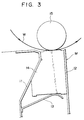
- Fig. 3 is a schematic view of an image sensor mounted in a facsimile.
- Figs. 4A and 4B show packs of image sensors constructed respectively in accordance with the prior art and the present invention.
- Fig. 5 is a cross-sectional view of the primary parts of an image sensor which is constructed in accordance with another embodiment of the present invention.
- Fig. 6 is an enlarged cross-sectional view of a base plate in the image sensor shown in Fig. 5.
- Fig. 7 is a side view of an image sensor constructed in accordance with still another embodiment of the present invention.
- Fig. 8 is a perspective view of a frame into which a transparent cover is being inserted, with some parts being omitted for clarification.
- Fig. 9 is a perspective view of a side plate being mounted on the end of the frame, with some parts being omitted for clarification.
- an image sensor which comprises a frame 1 of aluminum, a base plate 2 mounted in the lower portion of the frame 1 and a transparent cover 3 of glass mounted in the top portion of the frame 1.
- the base plate 2 includes a light emitting element 4 formed of an LED chip or the like formed thereon, a light receiving element 5 formed of a photodiode chip or the like similarly formed on the base plate 2, and any suitable wiring pattern formed over the surface of the base plate 2.
- An optical system (gradient index type lens array) 6 is biased and firmly held against the inner wall 1a of the frame 1 through a lens holding member 7 which is mounted in the frame 1.
- the light emitting element 4 is positioned vertically directly below the glass cover 3 while the optical system 6 is located having its optical axis inclined relative to the plane of the glass cover 3 by an angle q.
- the light receiving element 5 is positioned on the optical axis of the optical system 6.
- All of the light emitting element 4, light receiving element 5 and optical system 6 are elongated in the direction perpendicular to the plane of the drawing. Thus, the electrical signals will be obtained for one line at a time.
- data for the next line can be read out by the image sensor.
- the angle q included between the plane of the glass cover 3 and the optical axis of the optical system 6 is equal to about 60 degrees.
- a distance x from the original document W on the glass cover 3 to the surface of the base plate 2 receiving the reflected light rays (more accurately, the light receiving element 5) can be decreased to about 15% smaller than the conjugate length of the optical system 6. Therefore, the thickness of the image sensor can be reduced correpondingly. Since the light emitting and receiving elements 4 and 5 are located on the same base plate 2, the necessary number of base plates to be used in the same image sensor can be decreased. Since the light emitting and receiving elements 4 and 5 can be manufactured simultaneously on the same base plate, the number of steps for manufacturing the image sensor can be reduced. Even if the angle q is equal to any value other than 60 degrees, the distance x may be similarly reduced either more or less.
- the frame 1 has its cross-sectional configuration tapered toward the top thereof.
- the frame 1 has one inclined side wall which is engaged at its inner face by the rod lens array 6 having the optical axis that is inclined relative to the plane of the transparent cover 3.
- the image sensor 14 When the image sensor is to be assembled into an electronic instrument, for example, into a facsimile machine, the image sensor 14 can be simply and easily positioned in place only by inserting it between two opposed guides 11 and 12 which have been previously formed in the main body M of the facsimile machine, as shown in Fig. 3. The image sensor 14 can be firmly urged and held against a platen roller 15 under the influence of a leaf spring 13 which has been mounted on the guide 11. The image sensor 14 can be more easily installed into the electronic instrument because the outline of the image sensor 14 is used as a reference on assembling.
- the image sensors 14 of the present invention may be packed in the box 16 by one more than the number of the image sensors 17 according to the prior art. This is because the tapered image sensors of the present invention can be positioned alternately upside down.
- the tapered configuration of the frame 1 in the image sensor is variable depending on the desired purpose. Particularly, if the angle of the inclined rod lens array 6 is changed from one to another, the configuration of the frame 1 can be varied.
- the image sensor constructed in accordance with the above embodiment of the present invention has the frame having its cross-sectional configuration tapered toward the transparent cover on the top thereof, it provides the following advantages:
- Fig. 5 shows another embodiment of an image sensor constructed in accordance with the present invention.
- the base plate 2 is upwardly biased by means of a U-shaped leaf spring 7 which is located on the inner bottom of the frame 1.
- the top face of the base plate 2 is engaged, at its periphery, by a shoulder 1b which is formed on the inner wall of the frame 1.
- the top face of the base plate 2 which includes light emitting and receiving elements 4 and 5 as in the first mentioned embodiment, is used as a reference on assembling.
- the focusing of the light receiving element 5 relative to the rod lens array 6 can be better performed irrespectively of the accuracy in the frame 1.
- the U-shaped leaf spring 17 consists of two U-shaped leaf spring elements each of which has a length equal to one-half of the length of the image sensor and which is inserted into the interior of the frame 1 from each end.
- the frame 1 has an inner wall located to the right as viewed in Fig. 5, on which a reflection plate 9 is mounted to conduct the light rays from the light emitting element 4 to the original document W in an efficient manner.
- the lens holding member 8 has a flat wall opposed to the reflection plate 9 and formed to have a light reflecting property.
- the light emitting and receiving elements 4 and 5 on the base plate 2 linearly extend along the length of the base plate 2.
- the frame 1 is also elongated along the length thereof and closed by a cover at each end.
- Each of the covers includes an inner light reflecting surface. In this embodiment, therefore, the optical path from the light emitting element 4 to the glass cover 3 will be completely enclosed by the light reflecting walls which may be made of any colored material having a good reflectivity such as white-colored resist.
- the base plate 2 comprises first and second base plate sections 21, 22.
- the first base plate section 21 comprises a base material 23, a copper pattern portion 24 formed over the base material 23, a green-colored resist layer 25 formed over the copper pattern portion 24 and a white-colored resist layer 26 formed on the green-colored resist layer 25 around the light emitting element 4.
- the light emitting element 4 is mounted on the white-colored resist layer 26 while the light receiving element 5 is mounted on the green-colored resist layer 25.
- the light emitting element 4 is located directly below the glass cover 3.
- the optical path is enclosed by the light reflecting walls 8 and 9.
- the surface of the base plate 2 around the light emitting element 4 is white-colored.
- the light receiving element 5 is located on the optical axis of the rod lens array 6.
- the surface of the base plate 2 around the light receiving element 5 is green-colored.
- the light rays are further reflected by the original document W toward the rod lens array 6. After passing through the rod lens array 6, the light rays are received by the light receiving element 5 wherein they are converted into electrical signals. Light rays which enter the green-colored resist layer 25 rather than the light receiving element 5 are absorbed by the green-colored resist layer 25 so that the light receiving property of the light receiving element 5 will not be adversely affected by irregular reflection.
- Fig. 7 is a schematic side view of the image sensor shown in Fig. 5 with one end plate being removed.
- the glass cover 3 is in the form of a plate glass of rectangular cross-section, the opposite top side edges being chamfered.
- the inner top edges of the frame 1 extend inwardly to accommodate themselves to the chamfered plate glass.
- the frame 1 further includes three circular notches 1c, 1d and 1e which are formed therein at each end and used to mount the end plate on the frame 1 in such a manner as will be described later.
- the glass cover 3 can be mounted in the frame 1 by inserting the glass cover 3 into the top of the frame 1 from one end.
- the aforementioned accommodation between the glass cover 3 and the top of the frame 1 facilitates the insertion of the glass cover 3 into the top of the frame 1. This also means that any possible strain in the frame 1 is additionally corrected by the insertion of the glass cover 3.
- an end plate 10 identical with each end of the frame 1 in outline and size is mounted on the corresponding end of the frame 1 by inserting pin 10c, 10d and 10e on the end plate 10 into the respective notches 1c, 1d and 1e of the frame 1.
- the opposite ends of the frame 1 are closed with the glass cover 3 being firmly fixed to the frame 1.
- the frame 1 and the glass cover 3 There may be some play between the frame 1 and the glass cover 3. However, when the image sensor is actually assembled into the electronic instrument such as a facsimile machine, the glass cover 3 will be held down against the frame 1 by the platen roller to eliminate any such play. In addition, the end plates 10 may be adhered or screwed to the frame 1 rather than being held by the pin-notch attachment described.
- An image sensor has a frame, a transparent cover which is mounted on the top of the frame and on which an original document is to be placed, and a base plate disposed within the frame. On the base plate, there are mounted a light emitting section, a lens for condensing the reflective light and a light receiving section.
- the base plate is disposed within the frame so that the light emitting section is located directly below the transparent cover and the optical axis of the condensing lens is inclined relative to the plane of the transparent cover.
- Light rays emitted from the light emitting section enter the transparent cover in a direction substantially perpendicular to the plane thereof and are reflected by the transparent cover slantingly toward the light receiving section.
- the condensing lens inclined relative to the plane of the transparent cover By arranging the condensing lens inclined relative to the plane of the transparent cover, the vertical distance between the light receiving section and the transparent cover can be reduced.
- the entire configuration of the frame is tapered toward the transparent cover on the top thereof.
- the condensing lens can be mounted and held in a recess formed in the top of the frame without the need for any adhesive.
Abstract
Description
- The present invention relates to an image sensor suitable for use in facsimile machines, optical character reader and the like.
- One of the conventional image sensors is shown in Fig. 1 which is a cross-sectional view of the primary parts of the image sensor, taken along a plane perpendicular to a line-like light receiving element. The image sensor comprises a
frame 30, atransparent cover 31 of for instance, glass mounted on the top of the frame, alight emitting element 32 on abase plate 33 which is mounted in theframe 30, and alight receiving element 34 on abase plate 35 which is mounted on the bottom of theframe 30. Thebase plate 33 also supports aresilient member 37 which resiliently urges and holds an optical system (gradient index type lens array) 36 against the inner wall 30a of theframe 30. The optical axis of theoptical system 36 is perpendicular to theglass cover 31 andbase plate 35. Theresilient member 37 also supports a sphericalplastic lens 38 directly above thelight emitting element 32. - An object to be detected A (e.g. original document) is placed on the
glass cover 31. Light rays emitted from thelight emitting element 32 irradiate the original document A on theglass cover 31 through theplastic lens 38 with an angle of about 45 degrees relative to the plane of theglass cover 31. Light rays are then reflected by the document A toward theoptical system 36 in the vertical direction. After passed through theoptical system 36, the light rays are received by thelight receiving element 34 wherein they are converted into electrical signals. - In such an arrangement, it is essential that a distance y from the original document A to the light receiving plane (more accurately, the light receiving element 34) is equal to at least the conjugate length of the
optical system 36. This is the primary cause of precluding the prior art image sensors from being reduced in size. - Since the aforementioned arrangement of the
base plates elements respective base plates - As can be seen from Fig. 1, the
frame 30 in the conventional image sensor are usually of rectangular, square or similar cross-section. If such an image sensor is to be installed into an electronic instrument such as a facsimile machine or the like, it is required to utilize threaded apertures and/or reference apertures which have been accurately formed in the image sensor frame and electronic instrument, considering the alignment of the image sensor frame with the platen roller of the electronic instrument. Such an installing operation is very cumbersome with the positional alignment being very difficult to accomplished. - In the aforementioned image sensor, the
base plate 33 was usually coated with a green-colored resist. Thus, the reflectivity at thebase plate 33 would be reduced. In order to increase the amount of light irradiating the object to be scanned, the amount of current in the image sensor must be increased or the light emitting element must be improved in performance. This raises a problem with respect to power consumption or manufacturing cost. - In the aforementioned image sensor of the prior art, the
glass cover 31 is usually bonded at its peripheral edge 31b to thetop face 30b of theframe 30 through any suitable adhesive. - The adhesive tends to deposit at portions of the
glass cover 31 other than its peripheral edge. An excess of the adhesive used tends to be forced out inwardly from the marginal area of theglass cover 31. This adversely affects the characteristic of light detection in the light receiving element. Since the process cannot go to the next step until the adhesive is completely dried, the use of adhesive is disadvantageous in improving the productivity. - It is therefore an object of the present invention to provide a small-sized image sensor which has a decreased distance perpendicular to the transparent cover, which can be more easily installed into any electronic instrument and which has an improved efficiency in packaging and/or transporting.
- Another object of the present invention is to provide an image sensor which has a minimized light loss.
- Still another object of the present invention is to provide an image sensor in which the transparent cover can be mounted without the need for any adhesive.
- To this end, the present invention provides an image sensor for irradiating light rays onto an object to be detected and for converting the light rays reflected from the object to be detected into electrical signals, the image sensor comprising:
a transparent cover on which an object to be detected is placed;
a light emitting section for irradiating light rays onto the object to be detected through the transparent cover;
a condensing lens for receiving and condensing the light rays reflected from the object to be detected through the transparent cover; a frame for mounting said transparent cover on the one end and mounting said light emitting section, condensing lens and light receiving section therein; and
a light receiving section for receiving the light rays from the condensing lens and for converting the received light rays into electrical signals,
the light emitting section being so arranged that the light rays emitted therefrom will enter the surface of the transparent cover in a direction substantially perpendicular thereto, the condensing lens being so arranged that the optical axis thereof is inclined relative to the surface of the transparent cover, and the cross-section of the frame being tapered toward the transparent cover. - The image sensor can be more easily installed into any electronic instrument such as a facsimile machine or the like and can be packaged more efficiently.
- It is preferred that the peripheral surface of a base plate around the portion thereof on which the light emitting section is mounted is increased in reflectivity. This reduces the light loss around this area.
- The lower portion of the frame is provided with a projection which contacts part of the surface of the base plate. The base plate is biased against the projection through a leaf spring engaging the underside of the base plate. This can simplify the manufacturing process.
- The transparent cover is housed within a recess formed on the top of the frame. Thus, the transparent cover can be mounted in the frame without the need for any adhesive which would be forced out inwardly from the top of the frame to deteriorate the transmissivity in the transparent cover.
- By the use of such an image sensor, one can more easily obtain an electronic instrument.
- Fig. 1 is a cross-sectional view of the primary parts of an image sensor constructed in accordance with the prior art.
- Fig. 2 is a cross-sectional view of the primary parts of an image sensor which is constructed in accordance with one embodiment of the present invention.
- Fig. 3 is a schematic view of an image sensor mounted in a facsimile.
- Figs. 4A and 4B show packs of image sensors constructed respectively in accordance with the prior art and the present invention.
- Fig. 5 is a cross-sectional view of the primary parts of an image sensor which is constructed in accordance with another embodiment of the present invention.
- Fig. 6 is an enlarged cross-sectional view of a base plate in the image sensor shown in Fig. 5.
- Fig. 7 is a side view of an image sensor constructed in accordance with still another embodiment of the present invention.
- Fig. 8 is a perspective view of a frame into which a transparent cover is being inserted, with some parts being omitted for clarification.
- Fig. 9 is a perspective view of a side plate being mounted on the end of the frame, with some parts being omitted for clarification.
- Referring first to Fig. 2, there is shown an image sensor which comprises a frame 1 of aluminum, a
base plate 2 mounted in the lower portion of the frame 1 and atransparent cover 3 of glass mounted in the top portion of the frame 1. Thebase plate 2 includes alight emitting element 4 formed of an LED chip or the like formed thereon, alight receiving element 5 formed of a photodiode chip or the like similarly formed on thebase plate 2, and any suitable wiring pattern formed over the surface of thebase plate 2. - An optical system (gradient index type lens array) 6 is biased and firmly held against the inner wall 1a of the frame 1 through a
lens holding member 7 which is mounted in the frame 1. In this embodiment, thelight emitting element 4 is positioned vertically directly below theglass cover 3 while theoptical system 6 is located having its optical axis inclined relative to the plane of theglass cover 3 by an angle q. The light receivingelement 5 is positioned on the optical axis of theoptical system 6. - In such an arrangement, light rays emitted from the
light emitting element 4 as shown by an alternate long and short dashed line in Fig. 2 impinge on an original document W which is an object to be detected placed on theglass cover 3 in the direction substantially perpendicular to the plane of the document W. The light rays are then reflected by the original document W in a direction inclined relative to theglass cover 3 by the angle q. The reflected light rays pass through theoptical system 6 and thereafter are received by thelight receiving element 5 wherein the light rays are converted into electrical signals. - All of the
light emitting element 4,light receiving element 5 andoptical system 6 are elongated in the direction perpendicular to the plane of the drawing. Thus, the electrical signals will be obtained for one line at a time. When the original document W is moved to the right or left as viewed in Fig. 2, data for the next line can be read out by the image sensor. - In this embodiment, the angle q included between the plane of the
glass cover 3 and the optical axis of theoptical system 6 is equal to about 60 degrees. In such a case, a distance x from the original document W on theglass cover 3 to the surface of thebase plate 2 receiving the reflected light rays (more accurately, the light receiving element 5) can be decreased to about 15% smaller than the conjugate length of theoptical system 6. Therefore, the thickness of the image sensor can be reduced correpondingly. Since the light emitting and receivingelements same base plate 2, the necessary number of base plates to be used in the same image sensor can be decreased. Since the light emitting and receivingelements - The frame 1 has its cross-sectional configuration tapered toward the top thereof. In other words, the frame 1 has one inclined side wall which is engaged at its inner face by the
rod lens array 6 having the optical axis that is inclined relative to the plane of thetransparent cover 3. - When the image sensor is to be assembled into an electronic instrument, for example, into a facsimile machine, the
image sensor 14 can be simply and easily positioned in place only by inserting it between twoopposed guides image sensor 14 can be firmly urged and held against aplaten roller 15 under the influence of aleaf spring 13 which has been mounted on theguide 11. Theimage sensor 14 can be more easily installed into the electronic instrument because the outline of theimage sensor 14 is used as a reference on assembling. - If a plurality of image sensors having the same lateral width are to be packed into a
package box 16, as shown in Figs. 4A and 4B, theimage sensors 14 of the present invention may be packed in thebox 16 by one more than the number of theimage sensors 17 according to the prior art. This is because the tapered image sensors of the present invention can be positioned alternately upside down. - The tapered configuration of the frame 1 in the image sensor is variable depending on the desired purpose. Particularly, if the angle of the inclined
rod lens array 6 is changed from one to another, the configuration of the frame 1 can be varied. - Since the image sensor constructed in accordance with the above embodiment of the present invention has the frame having its cross-sectional configuration tapered toward the transparent cover on the top thereof, it provides the following advantages:
- (1) Since the outline of the image sensor can be used as a reference on assembling it into the electronic instrument, the image sensor may be easily assembled into the electronic instrument.
- (2) Since the number of image sensors which may be housed within a package box is increased, the efficiency of transportation may be improved.
- Fig. 5 shows another embodiment of an image sensor constructed in accordance with the present invention. In this embodiment, the
base plate 2 is upwardly biased by means of aU-shaped leaf spring 7 which is located on the inner bottom of the frame 1. The top face of thebase plate 2 is engaged, at its periphery, by a shoulder 1b which is formed on the inner wall of the frame 1. In such a manner, the top face of thebase plate 2, which includes light emitting and receivingelements light receiving element 5 relative to therod lens array 6 can be better performed irrespectively of the accuracy in the frame 1. TheU-shaped leaf spring 17 consists of two U-shaped leaf spring elements each of which has a length equal to one-half of the length of the image sensor and which is inserted into the interior of the frame 1 from each end. - The frame 1 has an inner wall located to the right as viewed in Fig. 5, on which a
reflection plate 9 is mounted to conduct the light rays from thelight emitting element 4 to the original document W in an efficient manner. Thelens holding member 8 has a flat wall opposed to thereflection plate 9 and formed to have a light reflecting property. - The light emitting and receiving
elements base plate 2 linearly extend along the length of thebase plate 2. On the other hand, the frame 1 is also elongated along the length thereof and closed by a cover at each end. Each of the covers includes an inner light reflecting surface. In this embodiment, therefore, the optical path from thelight emitting element 4 to theglass cover 3 will be completely enclosed by the light reflecting walls which may be made of any colored material having a good reflectivity such as white-colored resist. - The
base plate 2 comprises first and secondbase plate sections base plate section 21 comprises abase material 23, acopper pattern portion 24 formed over thebase material 23, a green-colored resistlayer 25 formed over thecopper pattern portion 24 and a white-colored resistlayer 26 formed on the green-colored resistlayer 25 around thelight emitting element 4. Thelight emitting element 4 is mounted on the white-colored resistlayer 26 while thelight receiving element 5 is mounted on the green-colored resistlayer 25. - In such an arrangement, the
light emitting element 4 is located directly below theglass cover 3. The optical path is enclosed by thelight reflecting walls base plate 2 around thelight emitting element 4 is white-colored. Thelight receiving element 5 is located on the optical axis of therod lens array 6. The surface of thebase plate 2 around thelight receiving element 5 is green-colored. Thus, light rays emitted from thelight emitting element 4 are repeatedly reflected by the white-colored resistlayer 26 andlight reflecting walls glass cover 3. This means that the loss of light between the light emittingelement 4 and the original document W can be minimized. - The light rays are further reflected by the original document W toward the
rod lens array 6. After passing through therod lens array 6, the light rays are received by thelight receiving element 5 wherein they are converted into electrical signals. Light rays which enter the green-colored resistlayer 25 rather than thelight receiving element 5 are absorbed by the green-colored resistlayer 25 so that the light receiving property of thelight receiving element 5 will not be adversely affected by irregular reflection. - Fig. 7 is a schematic side view of the image sensor shown in Fig. 5 with one end plate being removed. As seen from Fig. 7, the
glass cover 3 is in the form of a plate glass of rectangular cross-section, the opposite top side edges being chamfered. The inner top edges of the frame 1 extend inwardly to accommodate themselves to the chamfered plate glass. The frame 1 further includes three circular notches 1c, 1d and 1e which are formed therein at each end and used to mount the end plate on the frame 1 in such a manner as will be described later. - The
glass cover 3 can be mounted in the frame 1 by inserting theglass cover 3 into the top of the frame 1 from one end. The aforementioned accommodation between theglass cover 3 and the top of the frame 1 facilitates the insertion of theglass cover 3 into the top of the frame 1. This also means that any possible strain in the frame 1 is additionally corrected by the insertion of theglass cover 3. - As shown in Fig. 9, an
end plate 10 identical with each end of the frame 1 in outline and size is mounted on the corresponding end of the frame 1 by insertingpin 10c, 10d and 10e on theend plate 10 into the respective notches 1c, 1d and 1e of the frame 1. Thus, the opposite ends of the frame 1 are closed with theglass cover 3 being firmly fixed to the frame 1. - There may be some play between the frame 1 and the
glass cover 3. However, when the image sensor is actually assembled into the electronic instrument such as a facsimile machine, theglass cover 3 will be held down against the frame 1 by the platen roller to eliminate any such play. In addition, theend plates 10 may be adhered or screwed to the frame 1 rather than being held by the pin-notch attachment described. - The image sensor of this embodiment is advantageous in the following respects:
- (1) Since the transparent cover can be mounted in the frame without need for any adhesive, the light detection in the light receiving element will not be adversely affected by any excessive forced out adhesive.
- (2) Since no adhesive is used to mount the transparent cover on the frame, the assembled parts can be transferred to the subsequent step immediately after the transparent cover has been mounted on the frame. This improves the producibility.
- (3) Since the transparent cover is inserted into the top of the frame, any strain in the frame can be corrected.
- An image sensor has a frame, a transparent cover which is mounted on the top of the frame and on which an original document is to be placed, and a base plate disposed within the frame. On the base plate, there are mounted a light emitting section, a lens for condensing the reflective light and a light receiving section.
- The base plate is disposed within the frame so that the light emitting section is located directly below the transparent cover and the optical axis of the condensing lens is inclined relative to the plane of the transparent cover. Light rays emitted from the light emitting section enter the transparent cover in a direction substantially perpendicular to the plane thereof and are reflected by the transparent cover slantingly toward the light receiving section. By arranging the condensing lens inclined relative to the plane of the transparent cover, the vertical distance between the light receiving section and the transparent cover can be reduced. The entire configuration of the frame is tapered toward the transparent cover on the top thereof. Thus, the image sensor can be more easily assembled into any electronic instrument. The light emitting section is enclosed by walls which are increased in reflectivity, resulting in an increase of the amount of irradiating light. The condensing lens can be mounted and held in a recess formed in the top of the frame without the need for any adhesive.
Claims (14)
- An image sensor for irradiating light rays onto an object to be reproduced and for converting the light rays reflected from the object to be reproduced into electrical signals, said image sensor comprising:
a transparent cover on which an object to be reproduced is placed;
a light emitting section for irradiating light rays onto the object to be reproduced through the transparent cover;
a condensing lens for receiving and condensing the light rays reflected from the object to be reproduced through the transparent cover; a frame for mounting said transparent cover on the one end and mounting said light emitting section, condensing lens and light receiving section therein; and
a light receiving section for receiving the light rays from the condensing lens and for converting the received light rays into electrical signals,
said light emitting section being so arranged that the light rays emitted therefrom will enter the surface of said transparent cover in a direction substantially perpendicular thereto, said condensing lens being so arranged that the optical axis thereof is inclined relative to the surface of said transparent cover, and the cross-section of said frame being tapered toward the transparent cover. - An image sensor as defined in claim 1 wherein said frame has one inner side wall located on the side of said light emitting section and extending perpendicular to the plane of said transparent cover, with the other inner side wall located on the side of said light receiving section being inclined relative to the plane of said transparent cover.
- An image sensor as defined in claim 2 wherein the other inner side wall located on the side of said light receiving section supports said condensing lens.
- An image sensor as defined in claim 1 wherein said light emitting and receiving sections are mounted on a single base plate.
- An image sensor as defined in claim 4 wherein the surface of said base plate around said light emitting section has an increased reflectivity.
- An image sensor as defined in claim 5 wherein the surface of said base plate around said light emitting section is white-colored.
- An image sensor as defined in claim 6 wherein the lower portion of said frame includes an inwardly projecting portion formed therein to contact part of the surface of said base plate and wherein said base plate is urged and held against said inwardly projecting portion through a leaf spring engaging the underside of said base plate.
- An image sensor as defined in claim 4, further comprising a partition for dividing a space above said base plate into two space portions for the respective light emitting and receiving sections.
- An image sensor as defined in claim 8 wherein said partition also serves as a lens holding member for said condensing lens.
- An image sensor as defined in claim 9 wherein the surface of said lens holding member located on the side of said light emitting section has an increased reflectivity.
- An image sensor as defined in claim 10 wherein the inner wall of said frame opposed to the surface of said lens holding member located on the side of said light emitting section supports a light reflecting plate.
- An image sensor as defined in claim 1 wherein said transparent cover is housed within a recess formed in the top of said frame.
- An image sensor as defined in claim 12 wherein the top opposite side edges of said transparent cover are chamfered and wherein said recess is formed to match the chamfered side edges of said transparent cover so that the chamfered side edges of said transparent cover are covered by the inner top edges of said frame.
- An electronic instrument comprising an image sensor for irradiating light rays onto an object to be reproduced and for converting the light rays reflected from the object to be reproduced into electrical signals, said image sensor comprising:
a transparent cover on which an object to be reproduced is placed;
a light emitting section for irradiating light rays onto the object to be reproduced through the transparent cover;
a condensing lens for receiving and condensing the light rays reflected from the object to be reproduced through the transparent cover; a frame for mounting said transparent cover on the one end and mounting said light emitting section, condensing lens and light receiving section therein; and
a light receiving section for receiving the light rays from the condensing lens and for converting the received light rays into electrical signals,
said light emitting section being so arranged that the light rays emitted therefrom will enter the surface of said transparent cover in a direction substantially perpendicular thereto, said condensing lens being so arranged that the optical axis thereof is inclined relative to the surface of said transparent cover, and the cross-section of said frame being tapered toward the transparent cover.
Applications Claiming Priority (8)
| Application Number | Priority Date | Filing Date | Title |
|---|---|---|---|
| JP156366/91 | 1991-06-27 | ||
| JP3156366A JPH057279A (en) | 1991-06-27 | 1991-06-27 | Image sensor |
| JP24541791A JPH0583468A (en) | 1991-09-25 | 1991-09-25 | Image sensor |
| JP245417/91 | 1991-09-25 | ||
| JP245418/91 | 1991-09-25 | ||
| JP24541891A JPH0583469A (en) | 1991-09-25 | 1991-09-25 | Image sensor |
| JP3249537A JP3021120B2 (en) | 1991-09-27 | 1991-09-27 | Image sensor |
| JP249537/91 | 1991-09-27 |
Publications (3)
| Publication Number | Publication Date |
|---|---|
| EP0520430A2 true EP0520430A2 (en) | 1992-12-30 |
| EP0520430A3 EP0520430A3 (en) | 1993-06-09 |
| EP0520430B1 EP0520430B1 (en) | 1996-12-18 |
Family
ID=27473409
Family Applications (1)
| Application Number | Title | Priority Date | Filing Date |
|---|---|---|---|
| EP92110681A Expired - Lifetime EP0520430B1 (en) | 1991-06-27 | 1992-06-25 | Image sensor |
Country Status (2)
| Country | Link |
|---|---|
| EP (1) | EP0520430B1 (en) |
| DE (1) | DE69215974T2 (en) |
Cited By (6)
| Publication number | Priority date | Publication date | Assignee | Title |
|---|---|---|---|---|
| EP0573984A1 (en) * | 1992-06-11 | 1993-12-15 | Canon Kabushiki Kaisha | Contact type image sensor, producing method of the same, and information processing apparatus |
| EP0653876A1 (en) * | 1993-10-14 | 1995-05-17 | Canon Kabushiki Kaisha | Contact type image sensor |
| EP0874517A2 (en) * | 1997-04-25 | 1998-10-28 | Canon Kabushiki Kaisha | Image reading apparatus |
| US10524703B2 (en) | 2004-07-13 | 2020-01-07 | Dexcom, Inc. | Transcutaneous analyte sensor |
| US10610136B2 (en) | 2005-03-10 | 2020-04-07 | Dexcom, Inc. | System and methods for processing analyte sensor data for sensor calibration |
| US10813577B2 (en) | 2005-06-21 | 2020-10-27 | Dexcom, Inc. | Analyte sensor |
Citations (3)
| Publication number | Priority date | Publication date | Assignee | Title |
|---|---|---|---|---|
| DE3716809A1 (en) * | 1986-05-20 | 1987-11-26 | Sharp Kk | IMAGE READER |
| GB2228366A (en) * | 1989-02-21 | 1990-08-22 | Canon Kk | Photoelectric converter and image reading apparatus mounting the same |
| EP0438104A2 (en) * | 1990-01-17 | 1991-07-24 | Matsushita Electric Industrial Co., Ltd. | Image reading device |
-
1992
- 1992-06-25 EP EP92110681A patent/EP0520430B1/en not_active Expired - Lifetime
- 1992-06-25 DE DE69215974T patent/DE69215974T2/en not_active Expired - Fee Related
Patent Citations (3)
| Publication number | Priority date | Publication date | Assignee | Title |
|---|---|---|---|---|
| DE3716809A1 (en) * | 1986-05-20 | 1987-11-26 | Sharp Kk | IMAGE READER |
| GB2228366A (en) * | 1989-02-21 | 1990-08-22 | Canon Kk | Photoelectric converter and image reading apparatus mounting the same |
| EP0438104A2 (en) * | 1990-01-17 | 1991-07-24 | Matsushita Electric Industrial Co., Ltd. | Image reading device |
Cited By (42)
| Publication number | Priority date | Publication date | Assignee | Title |
|---|---|---|---|---|
| EP0573984A1 (en) * | 1992-06-11 | 1993-12-15 | Canon Kabushiki Kaisha | Contact type image sensor, producing method of the same, and information processing apparatus |
| US5489995A (en) * | 1992-06-11 | 1996-02-06 | Canon Kabushiki Kaisha | Contact type image sensor, producing method of the same, and information processing apparatus |
| EP0653876A1 (en) * | 1993-10-14 | 1995-05-17 | Canon Kabushiki Kaisha | Contact type image sensor |
| US5581076A (en) * | 1993-10-14 | 1996-12-03 | Canon Kabushiki Kaisha | Contact type image sensor with more-unified construction |
| EP0874517A2 (en) * | 1997-04-25 | 1998-10-28 | Canon Kabushiki Kaisha | Image reading apparatus |
| EP0874517A3 (en) * | 1997-04-25 | 1999-03-31 | Canon Kabushiki Kaisha | Image reading apparatus |
| US6295141B1 (en) | 1997-04-25 | 2001-09-25 | Canon Kabushiki Kaisha | Image reading apparatus |
| US10709363B2 (en) | 2004-07-13 | 2020-07-14 | Dexcom, Inc. | Analyte sensor |
| US10722152B2 (en) | 2004-07-13 | 2020-07-28 | Dexcom, Inc. | Analyte sensor |
| US11064917B2 (en) | 2004-07-13 | 2021-07-20 | Dexcom, Inc. | Analyte sensor |
| US10524703B2 (en) | 2004-07-13 | 2020-01-07 | Dexcom, Inc. | Transcutaneous analyte sensor |
| US11045120B2 (en) | 2004-07-13 | 2021-06-29 | Dexcom, Inc. | Analyte sensor |
| US10918315B2 (en) | 2004-07-13 | 2021-02-16 | Dexcom, Inc. | Analyte sensor |
| US11026605B1 (en) | 2004-07-13 | 2021-06-08 | Dexcom, Inc. | Analyte sensor |
| US10709362B2 (en) | 2004-07-13 | 2020-07-14 | Dexcom, Inc. | Analyte sensor |
| US10993642B2 (en) | 2004-07-13 | 2021-05-04 | Dexcom, Inc. | Analyte sensor |
| US11883164B2 (en) | 2004-07-13 | 2024-01-30 | Dexcom, Inc. | System and methods for processing analyte sensor data for sensor calibration |
| US10993641B2 (en) | 2004-07-13 | 2021-05-04 | Dexcom, Inc. | Analyte sensor |
| US10799158B2 (en) | 2004-07-13 | 2020-10-13 | Dexcom, Inc. | Analyte sensor |
| US10799159B2 (en) | 2004-07-13 | 2020-10-13 | Dexcom, Inc. | Analyte sensor |
| US10813576B2 (en) | 2004-07-13 | 2020-10-27 | Dexcom, Inc. | Analyte sensor |
| US10980452B2 (en) | 2004-07-13 | 2021-04-20 | Dexcom, Inc. | Analyte sensor |
| US10827956B2 (en) | 2004-07-13 | 2020-11-10 | Dexcom, Inc. | Analyte sensor |
| US10932700B2 (en) | 2004-07-13 | 2021-03-02 | Dexcom, Inc. | Analyte sensor |
| US10918314B2 (en) | 2004-07-13 | 2021-02-16 | Dexcom, Inc. | Analyte sensor |
| US10918313B2 (en) | 2004-07-13 | 2021-02-16 | Dexcom, Inc. | Analyte sensor |
| US10610137B2 (en) | 2005-03-10 | 2020-04-07 | Dexcom, Inc. | System and methods for processing analyte sensor data for sensor calibration |
| US11000213B2 (en) | 2005-03-10 | 2021-05-11 | Dexcom, Inc. | System and methods for processing analyte sensor data for sensor calibration |
| US10918316B2 (en) | 2005-03-10 | 2021-02-16 | Dexcom, Inc. | System and methods for processing analyte sensor data for sensor calibration |
| US10898114B2 (en) | 2005-03-10 | 2021-01-26 | Dexcom, Inc. | System and methods for processing analyte sensor data for sensor calibration |
| US10918318B2 (en) | 2005-03-10 | 2021-02-16 | Dexcom, Inc. | System and methods for processing analyte sensor data for sensor calibration |
| US10925524B2 (en) | 2005-03-10 | 2021-02-23 | Dexcom, Inc. | System and methods for processing analyte sensor data for sensor calibration |
| US10856787B2 (en) | 2005-03-10 | 2020-12-08 | Dexcom, Inc. | System and methods for processing analyte sensor data for sensor calibration |
| US10610136B2 (en) | 2005-03-10 | 2020-04-07 | Dexcom, Inc. | System and methods for processing analyte sensor data for sensor calibration |
| US10743801B2 (en) | 2005-03-10 | 2020-08-18 | Dexcom, Inc. | System and methods for processing analyte sensor data for sensor calibration |
| US10716498B2 (en) | 2005-03-10 | 2020-07-21 | Dexcom, Inc. | System and methods for processing analyte sensor data for sensor calibration |
| US10918317B2 (en) | 2005-03-10 | 2021-02-16 | Dexcom, Inc. | System and methods for processing analyte sensor data for sensor calibration |
| US10709364B2 (en) | 2005-03-10 | 2020-07-14 | Dexcom, Inc. | System and methods for processing analyte sensor data for sensor calibration |
| US10617336B2 (en) | 2005-03-10 | 2020-04-14 | Dexcom, Inc. | System and methods for processing analyte sensor data for sensor calibration |
| US11051726B2 (en) | 2005-03-10 | 2021-07-06 | Dexcom, Inc. | System and methods for processing analyte sensor data for sensor calibration |
| US10610135B2 (en) | 2005-03-10 | 2020-04-07 | Dexcom, Inc. | System and methods for processing analyte sensor data for sensor calibration |
| US10813577B2 (en) | 2005-06-21 | 2020-10-27 | Dexcom, Inc. | Analyte sensor |
Also Published As
| Publication number | Publication date |
|---|---|
| DE69215974T2 (en) | 1997-07-10 |
| EP0520430B1 (en) | 1996-12-18 |
| DE69215974D1 (en) | 1997-01-30 |
| EP0520430A3 (en) | 1993-06-09 |
Similar Documents
| Publication | Publication Date | Title |
|---|---|---|
| US5434682A (en) | Image sensor | |
| EP1659773B1 (en) | Contact-type image sensor | |
| US5182445A (en) | Contact type line image sensor | |
| US6259082B1 (en) | Image reading apparatus | |
| US9462150B2 (en) | Image read-in device with fastener to fasten transparent member retaining lens array assembly and light shield to board | |
| US9478090B2 (en) | Image sensor unit, image reading apparatus, and paper sheet distinguishing apparatus | |
| US6014231A (en) | Image sensor | |
| US9065961B2 (en) | Image sensor unit, image reading apparatus, and image forming apparatus | |
| EP1045329B1 (en) | Optical assembly having lens offset from optical axis | |
| JP2015073264A (en) | Illumination device, image sensor unit, image reading device and image formation device | |
| US7419274B2 (en) | Optical conduction unit and image reader using the same | |
| EP0520430B1 (en) | Image sensor | |
| US5965870A (en) | Image reading system with means for converging light from a plurality of light sources on a substantially same position to uniformly irradiate an object | |
| EP0100610B1 (en) | Illumination system | |
| US6081351A (en) | Image reading apparatus | |
| JPH1155456A (en) | Image reader | |
| US5157536A (en) | Optical apparatus having spring holding means for lenses | |
| JP4096421B2 (en) | Image reading device | |
| JPH05103157A (en) | Lighting device for image reader | |
| US20170295287A1 (en) | Manufacturing method of sensor unit and reading apparatus | |
| JP2000101781A (en) | Contact type image sensor unit | |
| JP3932068B2 (en) | Image reading device | |
| JP3058770B2 (en) | Image sensor | |
| JP2953595B2 (en) | Contact image sensor | |
| JP3307978B2 (en) | Image sensor |
Legal Events
| Date | Code | Title | Description |
|---|---|---|---|
| PUAI | Public reference made under article 153(3) epc to a published international application that has entered the european phase |
Free format text: ORIGINAL CODE: 0009012 |
|
| AK | Designated contracting states |
Kind code of ref document: A2 Designated state(s): DE FR GB |
|
| PUAL | Search report despatched |
Free format text: ORIGINAL CODE: 0009013 |
|
| AK | Designated contracting states |
Kind code of ref document: A3 Designated state(s): DE FR GB |
|
| 17P | Request for examination filed |
Effective date: 19930524 |
|
| 17Q | First examination report despatched |
Effective date: 19950612 |
|
| GRAG | Despatch of communication of intention to grant |
Free format text: ORIGINAL CODE: EPIDOS AGRA |
|
| GRAH | Despatch of communication of intention to grant a patent |
Free format text: ORIGINAL CODE: EPIDOS IGRA |
|
| GRAH | Despatch of communication of intention to grant a patent |
Free format text: ORIGINAL CODE: EPIDOS IGRA |
|
| GRAA | (expected) grant |
Free format text: ORIGINAL CODE: 0009210 |
|
| AK | Designated contracting states |
Kind code of ref document: B1 Designated state(s): DE FR GB |
|
| REF | Corresponds to: |
Ref document number: 69215974 Country of ref document: DE Date of ref document: 19970130 |
|
| ET | Fr: translation filed | ||
| PLBE | No opposition filed within time limit |
Free format text: ORIGINAL CODE: 0009261 |
|
| STAA | Information on the status of an ep patent application or granted ep patent |
Free format text: STATUS: NO OPPOSITION FILED WITHIN TIME LIMIT |
|
| 26N | No opposition filed | ||
| REG | Reference to a national code |
Ref country code: GB Ref legal event code: IF02 |
|
| PGFP | Annual fee paid to national office [announced via postgrant information from national office to epo] |
Ref country code: FR Payment date: 20080617 Year of fee payment: 17 |
|
| PGFP | Annual fee paid to national office [announced via postgrant information from national office to epo] |
Ref country code: GB Payment date: 20080625 Year of fee payment: 17 |
|
| PGFP | Annual fee paid to national office [announced via postgrant information from national office to epo] |
Ref country code: DE Payment date: 20090619 Year of fee payment: 18 |
|
| GBPC | Gb: european patent ceased through non-payment of renewal fee |
Effective date: 20090625 |
|
| REG | Reference to a national code |
Ref country code: FR Ref legal event code: ST Effective date: 20100226 |
|
| PG25 | Lapsed in a contracting state [announced via postgrant information from national office to epo] |
Ref country code: FR Free format text: LAPSE BECAUSE OF NON-PAYMENT OF DUE FEES Effective date: 20090630 |
|
| PG25 | Lapsed in a contracting state [announced via postgrant information from national office to epo] |
Ref country code: GB Free format text: LAPSE BECAUSE OF NON-PAYMENT OF DUE FEES Effective date: 20090625 |
|
| PG25 | Lapsed in a contracting state [announced via postgrant information from national office to epo] |
Ref country code: DE Free format text: LAPSE BECAUSE OF NON-PAYMENT OF DUE FEES Effective date: 20110101 |