EP0518524B1 - Ventil und seine Verwendung in einer Vorrichtung hergestellt aus Halbleitermaterial - Google Patents
Ventil und seine Verwendung in einer Vorrichtung hergestellt aus Halbleitermaterial Download PDFInfo
- Publication number
- EP0518524B1 EP0518524B1 EP19920304832 EP92304832A EP0518524B1 EP 0518524 B1 EP0518524 B1 EP 0518524B1 EP 19920304832 EP19920304832 EP 19920304832 EP 92304832 A EP92304832 A EP 92304832A EP 0518524 B1 EP0518524 B1 EP 0518524B1
- Authority
- EP
- European Patent Office
- Prior art keywords
- valve
- film
- gas
- substrate
- sacrifice layer
- Prior art date
- Legal status (The legal status is an assumption and is not a legal conclusion. Google has not performed a legal analysis and makes no representation as to the accuracy of the status listed.)
- Expired - Lifetime
Links
Images


Classifications
-
- F—MECHANICAL ENGINEERING; LIGHTING; HEATING; WEAPONS; BLASTING
- F16—ENGINEERING ELEMENTS AND UNITS; GENERAL MEASURES FOR PRODUCING AND MAINTAINING EFFECTIVE FUNCTIONING OF MACHINES OR INSTALLATIONS; THERMAL INSULATION IN GENERAL
- F16K—VALVES; TAPS; COCKS; ACTUATING-FLOATS; DEVICES FOR VENTING OR AERATING
- F16K99/00—Subject matter not provided for in other groups of this subclass
- F16K99/0001—Microvalves
-
- F—MECHANICAL ENGINEERING; LIGHTING; HEATING; WEAPONS; BLASTING
- F04—POSITIVE - DISPLACEMENT MACHINES FOR LIQUIDS; PUMPS FOR LIQUIDS OR ELASTIC FLUIDS
- F04B—POSITIVE-DISPLACEMENT MACHINES FOR LIQUIDS; PUMPS
- F04B43/00—Machines, pumps, or pumping installations having flexible working members
- F04B43/02—Machines, pumps, or pumping installations having flexible working members having plate-like flexible members, e.g. diaphragms
- F04B43/04—Pumps having electric drive
- F04B43/043—Micropumps
-
- F—MECHANICAL ENGINEERING; LIGHTING; HEATING; WEAPONS; BLASTING
- F15—FLUID-PRESSURE ACTUATORS; HYDRAULICS OR PNEUMATICS IN GENERAL
- F15C—FLUID-CIRCUIT ELEMENTS PREDOMINANTLY USED FOR COMPUTING OR CONTROL PURPOSES
- F15C5/00—Manufacture of fluid circuit elements; Manufacture of assemblages of such elements integrated circuits
-
- F—MECHANICAL ENGINEERING; LIGHTING; HEATING; WEAPONS; BLASTING
- F16—ENGINEERING ELEMENTS AND UNITS; GENERAL MEASURES FOR PRODUCING AND MAINTAINING EFFECTIVE FUNCTIONING OF MACHINES OR INSTALLATIONS; THERMAL INSULATION IN GENERAL
- F16K—VALVES; TAPS; COCKS; ACTUATING-FLOATS; DEVICES FOR VENTING OR AERATING
- F16K99/00—Subject matter not provided for in other groups of this subclass
- F16K99/0001—Microvalves
- F16K99/0003—Constructional types of microvalves; Details of the cutting-off member
- F16K99/0015—Diaphragm or membrane valves
-
- F—MECHANICAL ENGINEERING; LIGHTING; HEATING; WEAPONS; BLASTING
- F16—ENGINEERING ELEMENTS AND UNITS; GENERAL MEASURES FOR PRODUCING AND MAINTAINING EFFECTIVE FUNCTIONING OF MACHINES OR INSTALLATIONS; THERMAL INSULATION IN GENERAL
- F16K—VALVES; TAPS; COCKS; ACTUATING-FLOATS; DEVICES FOR VENTING OR AERATING
- F16K99/00—Subject matter not provided for in other groups of this subclass
- F16K99/0001—Microvalves
- F16K99/0034—Operating means specially adapted for microvalves
- F16K99/0042—Electric operating means therefor
- F16K99/0051—Electric operating means therefor using electrostatic means
-
- F—MECHANICAL ENGINEERING; LIGHTING; HEATING; WEAPONS; BLASTING
- F16—ENGINEERING ELEMENTS AND UNITS; GENERAL MEASURES FOR PRODUCING AND MAINTAINING EFFECTIVE FUNCTIONING OF MACHINES OR INSTALLATIONS; THERMAL INSULATION IN GENERAL
- F16K—VALVES; TAPS; COCKS; ACTUATING-FLOATS; DEVICES FOR VENTING OR AERATING
- F16K99/00—Subject matter not provided for in other groups of this subclass
- F16K2099/0073—Fabrication methods specifically adapted for microvalves
- F16K2099/0074—Fabrication methods specifically adapted for microvalves using photolithography, e.g. etching
-
- F—MECHANICAL ENGINEERING; LIGHTING; HEATING; WEAPONS; BLASTING
- F16—ENGINEERING ELEMENTS AND UNITS; GENERAL MEASURES FOR PRODUCING AND MAINTAINING EFFECTIVE FUNCTIONING OF MACHINES OR INSTALLATIONS; THERMAL INSULATION IN GENERAL
- F16K—VALVES; TAPS; COCKS; ACTUATING-FLOATS; DEVICES FOR VENTING OR AERATING
- F16K99/00—Subject matter not provided for in other groups of this subclass
- F16K2099/0082—Microvalves adapted for a particular use
-
- Y—GENERAL TAGGING OF NEW TECHNOLOGICAL DEVELOPMENTS; GENERAL TAGGING OF CROSS-SECTIONAL TECHNOLOGIES SPANNING OVER SEVERAL SECTIONS OF THE IPC; TECHNICAL SUBJECTS COVERED BY FORMER USPC CROSS-REFERENCE ART COLLECTIONS [XRACs] AND DIGESTS
- Y10—TECHNICAL SUBJECTS COVERED BY FORMER USPC
- Y10S—TECHNICAL SUBJECTS COVERED BY FORMER USPC CROSS-REFERENCE ART COLLECTIONS [XRACs] AND DIGESTS
- Y10S251/00—Valves and valve actuation
- Y10S251/901—Curtain type valves
-
- Y—GENERAL TAGGING OF NEW TECHNOLOGICAL DEVELOPMENTS; GENERAL TAGGING OF CROSS-SECTIONAL TECHNOLOGIES SPANNING OVER SEVERAL SECTIONS OF THE IPC; TECHNICAL SUBJECTS COVERED BY FORMER USPC CROSS-REFERENCE ART COLLECTIONS [XRACs] AND DIGESTS
- Y10—TECHNICAL SUBJECTS COVERED BY FORMER USPC
- Y10T—TECHNICAL SUBJECTS COVERED BY FORMER US CLASSIFICATION
- Y10T137/00—Fluid handling
- Y10T137/6416—With heating or cooling of the system
-
- Y—GENERAL TAGGING OF NEW TECHNOLOGICAL DEVELOPMENTS; GENERAL TAGGING OF CROSS-SECTIONAL TECHNOLOGIES SPANNING OVER SEVERAL SECTIONS OF THE IPC; TECHNICAL SUBJECTS COVERED BY FORMER USPC CROSS-REFERENCE ART COLLECTIONS [XRACs] AND DIGESTS
- Y10—TECHNICAL SUBJECTS COVERED BY FORMER USPC
- Y10T—TECHNICAL SUBJECTS COVERED BY FORMER US CLASSIFICATION
- Y10T137/00—Fluid handling
- Y10T137/8593—Systems
- Y10T137/87249—Multiple inlet with multiple outlet
Definitions
- the present invention relates to a valve and a semiconductor fabricating equipment using the same, and particularly, to an actuator for opening and closing action in a valve adapted to control a flow rate of fluid, and a semiconductor fabricating equipment for forming a semiconducting film on the surface of a substrate by switching different kinds of source gases using the valve.
- the actuator for a valve or the like used to control a flow rate of a trace of fluid, in Proceedings of the IEEE Micro ElectroMechanical System, pp95-98, 1990, wherein the actuator comprises a sheet having one end being fixed to serve as a valve body and an electrode which has a passage port and is disposed on the lower side of the sheet surface whereby the sheet is displaced by an electrostatic force for opening and closing the passage port.
- the above actuator is constituted of a dielectric with a passage port including a plate electrode on a silicon substrate, and a valve body made of a dielectric including a plate electrode for opening and closing the passage port, wherein the sheet is attracted to the electrode surface by an electrostatic force generated between the electrodes, to thereby close the passage port provided on a part of structure on the electrode side.
- the opening of the passage is effected by utilizing a restoring force of the sheet functioning as a spring.
- the time required for opening the passage port is restricted by the quickness of the returning of the sheet due to the restoring force thereof and is hence difficult to be made shortened.
- the electrostatic force acted in closing the passage port must be too large to resist the restoring force of the sheet functioning as a spring.
- the electrostatic force is inversely propotional to the square of the distance between the electrodes. Accordingly, in order to obtain a sufficient electrostatic force to resist the above restoring force, the above-mentioned conventional structure needs to makes smaller the distance between the sheet and the electrode located under the sheet up to a gap, for example, of several ten ⁇ m. Therefore, since a flow rate of fluid is restricted by the distance between the sheet and the electrode under the sheet, a valve using the conventional actuator has a difficulty to control a large flow rate of fluid.
- US 4 147 183 (on which the preamble of the claims 1 and 4 is based) describes a curtain value having a ribbon-like band which moves under the action of a pair of rollers, to cover and uncover the outlet port of the value.
- the band is bent into an S-shape around the rollers.
- the technique of forming a semiconducting film on a semiconductor substrate is an important process in the fabrication of semiconductor devices such as IC, and LSI.
- the epitaxial growth process requires switching of plural kinds of gases.
- the switching of gases in a semiconductor fabrication has been carried out with use of a valve 50 provided in a tube 51 connected with a gas bomb disposed separatedly from a vaccum chamber 49 internally including a substrate 48 (disclosed, for example, in Japanese Patent Laid-Open No. sho 63-136616).
- the epitaxial growth technique is required to form an extremely thinned film, for example, a superstructure having a layer thickness of at least 1 nm with accuracy of atomic order.
- the prior art includes a long pipe from a valve 50 to a vacuum chamber 49, which occurs a delay time between valve switching and gas-flow switching in the vacuum chamber, and which makes the change in gas pressure slow. Accordingly, for the purpose of forming a superstructure on a substrate by alternately introducing different kinds of gases within the vacuum chamber, the prior art has disadvantage of not sufficiently controlling the atomic arrangement of the superstructure and of taking a long period of time for film growth.
- the above-mentioned prior art has a large disadvantage accompanied by supplying gas from the gas introducing vessel.
- it has a difficulty to supply a reaction gas in a minimum amount required for epitaxial growth only in the vicinity of the surface of the substrate.
- This is due to the fact that there has been merely known such an opening and closing equipment as being in a grade of a shutter used in a Molecular Beam Epitaxy (MBE).
- MBE Molecular Beam Epitaxy
- the technique for making the semiconductor fabrication speedy, there has been proposed a technique of disposing a nozzle in the vicinity of a substrate to be processed, and of mechanically controlling the port of the nozzle for opening and closing action.
- the technique is disadvantageous in that the mechanical opening and closing action tends to yield pulsating current of fluid, that is, turbulent flow in a gas passage, which is unsatisfactory for the fabrication of the above mentioned micro-superstructure or the like.
- the present invention provides valves as set out in claims 1 and 4.
- the invention also provides a pump having such a valve
- valve defined by Claim 1 which includes a conductive film and electrodes as the film operating means disposed at both positions facing to upper and lower sides of the film surface, a voltage is applied from or to across the conductive film and the upper side electrode and to or from across the conductive film and the lower side electrode, thus crosswisely moving the inflexion point of the film with an electrostatic force.
- the valve includes a plurality of ports and by moving the inflexion point of the conductive film, the surface of the conductive film serves as a valve body for opening and closing the ports, to thereby form a valve for controlling a flow rate of fluid.
- the magnetic film of the valve defined by claim 4 can serve as a valve body for opening and closing the ports of that valve.
- the valve of the present invention functions to move the inflexion point of the film by the electrostatic force (or electromagnetic force) sequentially from the position where the film and electrode (or electromagnet) are in close proximity to each other. Consequently, even when the supporting means is long in height, that is, a distance between the upper and lower electrodes (or electromagnets) is enlarged, the film can be operated. Therefore, there can be suitably set the distance between the electrodes (or electromagnets) disposed on the upper and lower sides of the film to hence enlarge an interval between the passage port and the valve body, thus controlling a large flow rate of fluid. Furtheremore, since the opening and closing action in valve is irrespective of the restoring force of the film, it is possible to open and close the passage port of the valve with high speed by the electrostatic force (or electromagnetic force).
- the valve of the present invention comprises for example electrodes, an insulating layer and a metallic film and hence can be fabricated to the size of 10mm or less using semiconductor micro-processing technique. Also, a plurality of valves can be integrated in a unit structure. Furthermore, respective gas outlets of a plurality of the valves may have a matrix-like arrangement in a unit structure, which makes it possible to independently operate respective valves with electric signals.
- a channel with a depth of several 10 to 100 ⁇ m is formed on a silicon substrate by anisotropic etching, and an electrode pattern, insulating layer and fluid port are formed in the channel. Subsequently, a sacrifice layer is also formed in the channel, and a film serving as a valve body is formed on the sacrifice layer in such a manner as to be supported at both the ends by the silicon substrate other than the channel.
- the sacrifice layer under the film is selectively etched by solution. Consequently, the film is supported by the silicon substrate at only both the ends thereof, thus forming a film structure having an inflexion portion in the channel of the subsutrate. Subsequently, the thus film structure having the electrode pattern, insulating layer and fluid port is bonded with another substrate having an electrode pattern, insulating layer and fluid port, to thereby fabricate a micro-valve.
- the above-mentioned process is characterized by fabricating the micro-valve with use of two substrates.
- a silicon substrate formed with a hole by anisotropic etching or electric discharge machinning is assembled to a silicon substrate formed with a first sacrifice layer on the surface, thus obtaining a structure similar to the above-mentioned channel.
- a second sacrifice layer and a film are formed on the assembled substrates, thereby forming a film structure which is supported by the substrate at both the ends to thus form an inflexion portion, similarly to the above manner.
- the film structure thus fabricated may bonded with two substrates each having a fluid port and an insulating layer on an electrode pattern, to thus form a micro-valve.
- the present invention provides a semiconductor fabricating equipment or a thin-layer fabricating apparatus having at least one valve as defined above, wherein a sample substrate is mounted in a vacuum chamber and gas is supplied within the vacuum chamber by gas supplying means thus forming semiconducting layers on the surface of the substrate.
- the above gas supplying means includes: a first passage for introducing gas in the vacuum chamber; a valve of the present invention provided on the extreme end of the passage; a second passage for introducing exhaust gas outside the vacuum chamber.
- the above gas valve includes; a port through which necessary gas is supplied to the substrate out of the gas supplied through the first passage; a port through which exhaust gas is released in the second passage; and gas controlling means for controlling a ratio of necessary gas to exhaust gas.
- the above sample substrate and the valve are disposed within a vacuum chamber with an exhaust port.
- the valve is minituarized, and the gas port and housing thereof is made of a material with a chemival stability to withstand the baking temperature within the vacuum chamber.
- a plurality of ports for supplying gas to the sample substrate on the valve thus making the gas distribution in the vicinity of the surface of the substrate uniform.
- a valve mounting chamber for introducing the valve next to a semiconducting layer growth chamber.
- a micro-valve mounted at an extreme end of a pipe is baked under a vacuum similar to that of the growth chamber, and is then introduced into the thin film growth chamber.
- respective positions of the substrate and micro-valve can be suitably set.
- the semiconductor fabricating equipment of the present invention is so constituted that a valve is disposed in the vicinity of a sample stage to control the gas flow rate in the vicinity of the sample stage without any pipe.
- a valve is disposed in the vicinity of a sample stage to control the gas flow rate in the vicinity of the sample stage without any pipe.
- epitaxial growth can be effected with such a high speed as being comparable to that obtained by being injected through a nozzle.
- the valve is operated to distribute the gas supplied at a specified flow rate into a necessary gas for growth of semiconducting layers and an exhaust gas. Accordingly, there occurs no pulsating current of gas thereby stabilizing the gas supply, which enhances the accuracies of thickness of semiconducting layers and material composition.
- the valve is of the type defined in claim 1.
- the valve is thus small in the outer shape, has no friction of motion, and can be composed of heat resisting material being less liable to release gas from the surface, differently from an electromagnetic valve, air valve or the like. Accordingly, the valve can be directly mounted and operated within the vacuum chamber. As a result, since the valve can be located closely to the substrate within the vacuum chamber, reaction gas can be supplied to the necessary minimum space. This remarkably improves the controllability of gas pressure in the vicinity of the surface of the sample substrate, which makes it possible to accurately control the atomic arrangement of a growing superstructure, and also to shorten the time required for the film growth.
- each micro-valve can be independently opened and closed with electric signals. This provides such additional functions as selecting a gas to be introduced within a thin film growth chamber from several kinds of gases, and as introducing the selected gas to the thin film growth chamber from only a specified one among a plurality of outlets. Thus, a specified film can be formed on a specified region on the substrate.
- Figs. 1 and 2 is a perspective view including a partial cross section and a side cross sectional view showing an example of an actuator constituting a primary part of a valve according to the present invention, respectively.
- the actuator includes a ribbon-like conductive film 1, two film supporting structures 2-1 and 2-2 for supporting both the ends of the film, and upper and lower operating units 3-1 and 3-2 respectively supported by the supporting structures 2-1 and 2-2 for operating the film 1.
- the film 1 is supported in such a manner as to form a S-shaped inflexion portion within the film 1,and accordingly,the length of the film 1 is set to be longer than an interval between the film supporting structures 2-1 and 2-2 with a height of, for example, 3mm.
- the film 1 is operated by the operating units 3-1 and 3-2 in such a manner that the curved plane (inflexion portion) 1-S is moved.
- the operating units 3-1 and 3-2 are constituted such that the portions facing to the upper and lower surfaces of the film 1 are made to be flat, respectively.
- the lower surface of the film 1 being in contact with the upper surface of the lower operating unit 3-2 is separated from the operating unit 3-2 sequentially in the direction from the supporting structure 2-1 to 2-2 side, thus moving the curved plane 1-S to the supporting structure 2-2 side.
- the actuator includes the operating unit 3-1 having an electrode disposed on the upper side of the conductive film 1 through an insulating layer 4 of a thickness of 2 ⁇ m or less, and the operating unit 3-2 having an electrode disposed on the lower side of the conductive film through an disposed on the lower side of the conductive film through an insulating layer 5 of a thickness of 2 ⁇ m or less.
- the S-shaped inflexion portion 1-S of the film 1 supported by the film supporting structures 2-1 and 2-2 is crosswisely moved by the electrostatic force.
- a translucent electrode made of ITO (Indium Tin Oxide) may be used as the electrode of the electrostatic actuator, which makes easy the observation of movement of the S-shaped plane caused by the applied voltage to thereby support the maintenance.
- the height of the supporting structures 2-1 and 2-2 is determined based on the thickness of the film 1, curvature radius of the curved plane, loss resistance caused by fluid flow and the like. In general, with the thinned thickness of the film 1 , the reduced elastic coefficient, and the increased curvature radius of the curved plane, the height of the film 1 can be reduced.
- each of the insulating films 4 and 5 needs a thickness enough to resist against dielectric breakdown in applying a voltage across the conductive film 1 and the electrode for operating the film 1.
- the insulating layer 4 and 5 can be formed by using the conventional technique of evaporation or chemical reaction growth of an insulation material, holding of an insulating sheet, coating of insulating agent or the like.
- the insulating material may be coated not only on the electrodes of the operating units 3-1 and 3-2 but also on the surface of the film 1.
- the material of the conductive film there is used a film made of a composite material sticked with the above conductive material.
- the film comprises; a metallic film of aluminum, gold, platinum, chrome, iron, nickel, permalloy, or molybdenum; an alloy film made of a stainless steel or the like ; and a film of polyimide resin, polyester, silicon, silicon nitride, silicon oxide, PBN (Pyrolytic Boron Nitride) or the like, on a surface or surfaces of which such a metallic or alloy film is formed.
- Fig. 3 is a perspective view including a partial cross section showing another example of an actuator constituting a primary part of a valve according to the present invention.
- the film 1 includes two inflexion planes 1-1i and 1-2i each having an integral-sign-shape of a smooth slope,and the other structure is the same as in Fig. 1.
- Each of the two inflexion planes 1-1i and 1-2i has a smooth and simple curvature radius compared with the S-shaped plane, and is easily fabricated. Also, the curvature radius is made larger, and the gap of two operating units in which the film acts can be reduced. Therefore, the actuator of this example is adapted for miniaturization of the valve.
- the film 1 having the curved plane formed in a S-shape has an effect that, because the bend thereof is pushed between the surfaces of the operating units located on the upper and lower sides of the film, the film 1 is prevented from being deflected with its dead weight when not being attracted by the operating units. Accordingly, it has an advantage of enlarging the interval between two supporting structures twice in the case of the integral -sign-shape.
- the shape of the curved plane of the film 1 is selected to be the integral -sign-shape or the S-shape.
- Fig. 4 is a cross section showing a further example of an actuator constituting a primary part of a valve according to the present invention. This example is characterized by operating the inflexion plane of the film by utilizing electromagnetic force as the film operating means.
- a film 7 is composed of a magnetic metallic film made of permalloy having a thickness of 5 ⁇ m.
- An operating unit includes electromagnets 8-1 and 8-2 respectively disposed on the upper and lower sides of the magnetic film 7. By switching the current flow from or to the electromagnet 8-1 to or from the electromagnet 8-2 with a switching circuit 9, a S-shape plane 7-1 of the magnetic film 7 is crosswisely moved by the electromagnetic force.
- the magnetic film 7 is made of a magnetic film of iron, nickel, or an alloy thereof such as permalloy, or a composite material obtained by coating or evaporating the powder of the above metal or alloy or mixture thereof on the film of polyimide, polyester, silicon, silicon nitride, or silicon oxide.
- a superconductive material may be used as the magnetic material.
- an electro magnet or superconductive magnet may be used as the film operating unit to operate the film by applying current to a coil pattern formed on the upper and lower surfaces of the film.
- the film 7 may be made of a shape memory alloy.
- the film made of the shape memory alloy previously storing the flat shape is plastically deformed into a S-shape in low temperatures, and both the ends thereof are rigidly supported to thus assemble an actuator, and thereafter, the film is heated at a martensite transformation temperature or more.
- the actuator can be assembled while deforming the film into a S-shape, to thereby make easy the fabrication process.
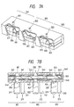
- Fig. 5 is a perspective view including a partial cross section showing an example of a valve according to the present invention.
- a valve in Fig. 5, includes a bendable metallic film 1 serving as a valve body, supporting structures 2 for supporting both the ends of the film 1, side walls 11 of the valve (the broken-out section shows the state of removing the side wall), and a pair of upper and lower plate electrodes 12 and 12' respectively each having an insulating film on the surface facing to the film 1.
- the flat electrodes 12 and 12' are provided with outlets 13 and an exhaust port 14, respectively.
- the outlets 13 and the exhaust port 14 can be opened and closed.
- a part of the film 1 serves as a valve body for opening and closing the passage ports 13 and 14.
- the metallic film 1 is made of stainless steel having a thickness of 5 ⁇ m.
- the flat electrodes 12 and 12′ are made of a single crystalline silicon wafer doped with impurities, and their surfaces to be brought in contact with the film 1 are insulated with thermal oxidized films having a thickness of approximately 1.5 ⁇ m, respectively.
- the valve is opened and closed by applying a direct voltage of several volts across the film 1 and upper or lower electrode, and consequently the flow-out of gas is switched to the outlets 13 or the exhaust port 14.
- the valve used for flow control, naturally needs to determine its material and dimensions based on the necessary flow rate, used pressure, kinds of gases and the like.
- the pressure drop and conductance in the passage is due to the cross section of the ports and the amount of the gap between two operating units for operating the film.
- the valve of this example has a feature of suitably determining these parameters.
- the time required for opening and closing the valve is to be within several tens milli-seconds.
- the material of the film 1 is preferably selected according to the kinds of the used gases.
- the thickness of the film 1 is preferably determined based on the magnitude of the load exerted on the film surface due to the pressure difference, and allowable deformed amount of the film surface.
- this example involves the structural modifications such as change in number of ports and in combination thereof, and functional alternation.
- Figs. 6A and 6B are schematic cross sectional views of the valve as shown in Fig. 5 for explaning the operation thereof.
- Fig. 6A shows the state where gas is made to flow-out from outlets 13 when a voltage is applied from a power supply 16 to a lower electrode 12'side.
- Fig. 6B shows the state where gas is made to flow-out from an exhaust port 14 when a voltage is applied from a power supply 17 to an upper electrode 12 side.
- the evacuation of the passage on the exhaust side can be effected, as required.
- the material used in the above-mentioned gas valve has the chemically stabilized surface enough to withstand the temperature of approximately 300°C of the baking carried out for increasing the degree of vacuum in a vacuum chamber.
- Figs. 7A and 7B are a perspective view including a partial cross-section and a cross sectional view of an example of an integrated gas valve according to the present invention.
- This embodiment is commonly provided with a plurality of valves in a matrix-like arrangement according to plural kinds of gases thereby alternately introducing gases into a semiconducting layer growth chamber.
- these figures show only the case in which three valves are integrated into a unit structure.
- valves 301, 302 and 303 operated according to the same principle are integrated, and are provided with gas supply pipings 311, 312 and 313, and exhaust pipings 321, 322 and 323, respectively.
- the valve 301 includes a bendable metallic film 331 serving as a valve body, and a pair of plate electrodes 341 and 344 each having an insulating layer 340 on the surface.
- a gas outlet 351 and exhaust port 356 are provided on the parts of a pair of the electrodes 341 and 344, respectively. Gas is supplied from a gas supply port 361.
- the metallic film 331 is made of stainless steel having a thickness of 5 ⁇ m.
- the plate electrode 341 is made of a single crystalline silicon wafer doped with impurities for reducing resistivity or a metallic thin film formed on a single crystalline silicon wafer.
- SiO 2 films each having a thickness of 0.5 to 2.5 ⁇ m on the surfaces of the plate electrodes 341 and 344 being contact with the metallic film 331.
- a SiC plate may be used in place of the above insulating layer.
- valve 301 by switching the voltage of 50 to 300 V applied across the film and the upper or lower electrode, the gas flow can be switched from or to the outlet 351 and to or from the exhaust port 356.
- the valves 302 and 303 are made of the same material as that of the valve 301, and are provided with metallic films 331 and 333, outlets 352 and 353, and exhaust ports 357 and 358, respectively.
- the exhaust ports 356, 357, 358 are connected with exhaust tubes 321, 322 and 323, respectively.
- the supply ports 361, 362 and 363 are connected with the gas supply tubes 311, 312 and 313, respectively.
- Fig. 7B only the gas 372 is introduced in a thin film growth chamber, and the other gases 371 and 372 are exhausted.
- the valve 302 shows the case where a voltage is applied across the lower electrode 344 and the film 332 which allows gas to flow-out from the outlet 352.
- the valve 303 shows the case where a voltage is applied across the upper electrode 343 and the film 333, which allows gas to flow-out from the exhaust port 358.
- the upper electrode, lower electrode and film of each valve are insulated from each other.
- the gas to be introduced into the thin film growth chamber can be selected.
- the integral valve of this example makes it possible to switch plural kinds of gases by the valve with a small capacity.
- a plurality of valves can be provided on the wall surface of the growth chamber or within the growth chamber.
- Fig. 8 is a cross sectional view of another example of a laminate type integrated gas valve according to the present invention.
- This is a laminated type integrated gas valve obtained by laminating the integrated valves as shown in Figs. 7A and 7B in a mutistage, and has such functions as of selecting the gas to be introduced into a semiconducting layer growth chamber from several kinds of gases 371, 372 and 373, and of introducing the selected gas from only the specified outlet among plural number of outlets 411, 412 and 413 to the thin film growth chamber.
- the laminated integrated valve includes two integrated valves 431 and 433, and a gas channel structure 432 for connecting the integrated valves 431 and 433 to each other.
- the integrated valve 433 includes three valves 441, 442 and 443.
- the gas to be introduced into a semiconducting layer growth chamber is selected from three kinds of gases 371, 372 and 373.
- FIG. 7A and 7B there is shown the case where only the gas 371 supplied to the valve 441 is introduced to the gas channel structure 432 and the other gases 372 and 373 are exhausted.
- the construction thereof is substantially similar to that of the integrated valves as shown in Figs. 7A and 7B. Accordingly, the same parts are indicated at the same numerals and the explanation thereof is omitted.
- the gas channel structure 432 includes a first gas channel for distributing the gas from a plurality of outlets of the integrated valve 433 into a plurality of supply ports 451, 452 and 453, and a second gas channel 470 for collectively exhausting (471) the gas from a plurality of exhaust ports of the integrated valve 431.
- the first gas channel and the second gas channel 470 are independently formed in the gas channel structure 432.
- the gas 371 selected by the integraed valve 433 is introduced to respective valves 446, 447 and 448 of the integrated valve 431 through the first channel of the gas channel structure 432 and a plurality of supply ports 451, 452 and 453 of the integrated valve 431.
- the gas 371 is then introduced from only the specified outlet among plural outlets 411, 412 and 413 to a semiconducting layer growth chamber.
- the upper integrated valve is constituted such that voltages applied on respective valves 446, 447 and 448 are controlled to switch the valves 446, 447 and 448. As a result, the outlets through which gas is introduced into the growth chamber can be selected.
- valve 8 shows the case where valves 446 and 448 are opened and the valve 447 is closed, which causes the selected gas 371 to be introduced into the growth chamber from the outlets 411 and 413.
- the gas not to be introduced into the thin fim growth chamber is exhausted through an exhaust channel 470 formed in the gas channel structure 432.
- the laminated type integrated valve makes it possible to select the gas to be introduced into the thin film growth chamber among various kinds of gases, and to introduce the selected gas into the growth chamber from the specified outlet among a plurality of outlets, thus enabling the formation of the thin film at the specified region on the substrate.
- the diameter and pitch of the outlet is spcified to be 10 ⁇ m and 1mm, respectively.
- the gas to be introduced into the thin film growth chamber using the laminated integrated valve approximately 10x10 ⁇ m 2 of the thin film is selectively formed on the substrate at a pitch of 1mm.
- the avarage free path of the gas introduced from the outlet is sufficiently long compared with the distance between the outlet and the substrate.
- Figs. 7A and 7B, and Fig. 8 respective valves are arranged in a single line to simplify the drawings; however, in actual, the outlets of a plurality of valves are set in a matrix-like arrangement toward a plane.
- Figs. 9a to 9k show fabricating processes of an example of a valve fabricating method according to the present invention. Hereinafter, the fabricating processes will be described in detail.
- a channel 120-1 having a cross width of 5mm, length of 10mm and depth of approximately 50 to 100 ⁇ m is formed on a silicon wafer 110-1 having a thickness of 39 ⁇ m by anisotropic etching.
- the etchant used in the anisotropic etching is a 40% potassium hydroxide, and the temperature of the solution is kept at 70°C.
- the crystal face orientation of the side wall of the channel is to be (111).
- a fluid port 125 and an aluminum electrode pattern 121 are formed in the channel 120-1 formed in (1) by photolithography, CVD, or sputtering.
- An insulating layer 122 made of a silicon oxide film or silicon nitride film is formed on the electrode pattern 121 to a thickness of several ⁇ m by sputtering or CVD.
- the fluid port 125 may be formed by techiniques other than etching, such as, electric discharge machinning.
- a photoresist 130-1 is spin coated on the silicon wafer 110-1 having the channel of a depth of approximately 50 to 100 ⁇ m formed with the electrode pattern and insulating layer, which are fabricated in (2).
- the viscosity of the photoresist and the rotational number of a spinner are determined in such a manner that the slope of the wall of the channel 120-1 is smoothly coated with the resist.
- the photoresist After coating on the silicon wafer, the photoresist is subjected to patterning by exposure and developing. Consequently, the photoresist 130-1 remains only on the channel 120-1 of the silicon wafer, which serves as a sacrifice layer.
- a metallic film 140 made of aluminum, nickel or the like to a thickness of several ⁇ m by evaporation, sputtering, CVD, or the like.
- the metallic thin film thus formed is subjected to pattering.
- the silicon wafer 110-1 is then dipped in an etching solution to selectively etch only the photoresist 130-1 under the metallic thin film, so that the metallic film is formed into such a bridge structure as to be supported at its both ends by the silicon wafer.
- Another silicon wafer 110-2 having a fluid port 125 and an insulating layer 122 on an electrode pattern 121 is bonded to the silicon wafer 110-1 having the metallic film in a matrix-like arrangement in the channel fabricated in (4), to thus fabricate a film electrostatic valve having a bend plane, as shown in Figs. 9i to 9k.
- the silicon wafer 110-2 is formed with a projection having a height equal to a depth of the channel 120 of the silicon wafer fabricated in (4).
- an adhesive agent there is used a polyimide resin capable of keeping its adhesiveness under high temperatures of 100 to 300°C or lead glass capable of acting as an adhesive under comparatively low temperatures of 300 to 400°C.
- Fig. 9k shows a three-way valve mechanism wherein fluid ports are provided on the upper and lower electrode plates, and gas inlets are provided on the upper and lower electrode plates or side walls of the valve, respectively.
- valve capable of discretly changing the gas flow accompanied by movement of the film. Also, by setting a plurality of the above-mentioned valves on the silicon wafer in a matrix-like arrangement, it is possible to fabricate the integrated flow control element.
- Figs. 10a to 10k show fabrication processes of another example of a valve fabricating method according to the present invention.
- the example as shown in Figs. 9a to 9k is characterized by fabricating the film having a S-shape plane in the channel 120-1 formed on the silicon wafer 10-1 by etching, and consequently has the following disadvantages:
- this example as shown in Figs. 10a to 10k uses two silicon wafers and two sacrifice layers and forms a micro-valve having the channel structure similar to the above-mentioned example as shown in Figs. 9a to 9k.
- a first thin silicon wafer 110-3 having a face orientation of (100) and a thickness of 220 ⁇ m is formed with a hole 150-1 using anisotropic etching or electric discharge machinning, as shown in Figs. 10a and 10b.
- the etchant used in the anisotropic etching is 40% potassium hydroxide, and the temperature of the solution is kept at 70°C .
- a photoresist 131-1 being a first sacrifice layer is spin coated on the surface of a second silicon wafer 110-4, as shown in Fig. 10i.
- the silicon wafer 110-3 having the hole 150-1 is then located on the photoresist 131-1 of the second wafer 110-4.
- the two silicon wafers are aligned to be then temporarily bonded, as shown in Fig. 10c.
- the thickness 220 ⁇ m of the silicon wafer 110-3 is equivalent to the stroke of the valve, to thus obtain the valve with a large stroke.
- a photoresist (second sacrifice layer) is spin coated on the two silicon wafers 110-3 and 110-4 having the channel with a depth of 220 ⁇ m fabricated in (1), as shown in Fig 10 d.
- the viscosity of the photoresist and rotational number of the spinner is determined so as to smoothly coat the wall slope of the channel with the resist. Subsequently, the photoresist is subjected to pattering by exposure and developing. Thus, the photoresist 130-2 (second sacrifice layer) remains only in the channel of the silicon wafer, which serves as the sacrifice layer, as shown in Fig. 10d.
- a metallic film 140 made of aluminum, nickel or the like is formed on the two silicon wafers after photoresist patterning fabricated in (2) to a thickness of several ⁇ m by evaporation, sputtering, CVD or the like. After that, the metallic film 140 is subjected to patterning by photolithography, as shown in Fig. 10e.
- the two silicon wafers 110-3 and 110-4 are dipped in an etching solution, so that only the photoresist 130-2 under the metallic film and the photoresist 131-1 between the silicon wafers 110-3 and 110-4 are selectively etched. Accordingly, the two silicon wafers are separated from each other, thus forming the metallic film having a bridge structure of being supported at only both the ends by the silicon wafer 110-3, as shown in Fig. 10f.
- Two silicon wafers 110-5 and 110-6 each having a port 125 and an insulating layer 122 on an electrode pattern 121 are aligned and bonded on both sides of the silicon wafer 110-3 (having the metallic thin film formed into a bridge shape at the hole portion) fabricated in (3), to thus fabricate the valve having the film with a bend portion, as shown in Figs. 10g, 10j, 10k and 10h.
- the silicon wafer 110-6 has a projection 180-2 with a height of 220 ⁇ m equal to the depth of the hole (thickness of the silicon wafer 110-3).
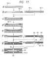
- FIGs. 11a to 11k show fabrication processes of a further example of a valve fabricating method according to the present invention.
- a film electrostatic micro-valve of this example is obtained by fabricating a S-shaped film using two silicon wafers in the same manner as shown in Example 8 expect the following point. Namely, as shown in Fig. 11b, when a silicon wafer 110-3 having a hole 150-1 is temporarily bonded on a silicon wafer 110-4 having a photoresist being a sacrifice layer, the bonded surface of the silicon wafer 110-3 is reversed to that shown in Fig. 10b.
- this example involves a difficulty in forming the photoresist 130-3 in a channel after bonding the two silicon wafers, as shown in Fig. 11d.
- this example has an effect that the film is less liable to be brought in close-contact with the slope of the hole.
- it is possible to easily fabricate a structure of supporting both the ends of the film by the silicon wafer, as shown in Fig. 11f.
- Figs. 12a to 12k show fabricating processes of a still further example of a valve fabricationg method capable of suitably setting the valve stroke described in the Examples 8 and 9.
- the fabrication methods according to Examples 8 and 9 are disadvantageous in that since the valve stroke is equivalent to the thickness of the silicon wafer 110-3 having a hole 150-1, it is determined by the thickness of the silicon wafer used.
- several types of processes of patterning, etching and the like are added to the processes shown in the Examples 8 and 9, to suitably determine the stroke of the micro-valve.
- this fabrication method will be described.
- a step 120-2 is formed on the rear surface of a silicon wafer 110-7 having a thickness of 390 ⁇ m by anisotropic etching, as shown in Fig. 12b. Subsequently, a hole 150-2 is formed on a part of the step 120-2 using anisotropic etching or electric discharge machinning again, as shown in Fig. 12b.
- the etchant used in the anisotropic etching is 40% potassium hydroxide, and the temperature of the solution is kept at 70 °C.
- the face orientation of the silicon wafer surface is (100), and the face orientation of the slope of the hole is (111).
- a photoresist 131-2 serving as a first sacrifice layer is spin coated on the surface of a silicon wafer 110-8 having a projection with a height equal to that of the step 120-2 formed on the rear surface of the silicon wafer 110-7, as shown in Fig. 12i.
- the silicon wafer 110-7 having the hole is located on the photoresist 131-2 of the silicon wafer 110-8, and the two wafers 110-7 and 110-8 are aligned and temporarily bonded, as shown in Fig. 12c.
- the two silicon wafers 110-7 and 110-8 there can be formed the same channel as that of Example 7 as shown in Figs. 9a to 9 b.
- the valve stroke is obtained by substracting the height of the step 120-2 formed on the rear surface from the thickness of the silicon wafer 110-7. Accordingly, by suitably controlling the etching amount for the rear surface, the valve stroke can be suitably determined.
- the stroke is 300 ⁇ m or 250 ⁇ m.
- a photoresist layer 130-3 (second sacrifice layer) is spin coated on the temperarily bonded two silicon wafers 110-7 and 110-8 having the channel 150-2 with, for example, a depth of 30 ⁇ m fabricated in (1), as shown in Fig. 12d.
- the viscosity of the photoresist and the rotational nember of a spinner is determined so as to smoothly coat the slope surface of the channel with the photoresist.
- the photoresist 130-3 (second sacrifice layer) remains only in the channel of the silicon wafer, which serves as a sacrifice layer.
- a metallic thin fim 140 made of aluminum, nickel or the like having a thickness of several ten ⁇ m is formed on the two silicon wafers 110-7 and 110-8 after photoresist patterning fabricated in (2) by evaporation, sputtering, CVD or the like.
- the metallic thin film is then subjected to patterning by photolithography, as shown in Fig 12e.
- the two silicon wafers 110-7 and 110-8 are dipped into etching solution so as to selectively etch only the photoresist 130-3 under the metallic thin film and the photoresist 131-2 between the silicon wafers 110-7 and 110-8. Consequently, the two silicon wafers are separated from each other, and the metallic thin film is formed into a bridge structure of being supported at both the ends by the silicon wafer 110-7, as shown in Fig. 12f.
- a channel (not shown) through which the etching solution for the sacrifice layer easily enters in the silicon wafer 110-8, so that the sacrifice layer can be uniformly etched for a shortened time.
- the silicon wafer 110-7 (having the metallic thin film formed into a bridge shape at a hole portion) fabricated in (3) is bonded on both the sides with a silicon wafer 110-9 having a fluid port and an electrode pattern covered with an insulating layer on the surface of a projection 190, and a silicon wafer 110-10 having a fluid port, an electrode covered with an insulating layer, and a projection 180-4, to thus fabricate a valve having the film with a bend plane, shown in Figs. 12f, 12g, 12h, 12j and 12k.
- the height of the projection 180-4 of the silicon wafer 110-10 is equivalent to the stroke of the valve.
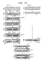
- Figs. 13a to 13m show fabricating processes of an additional example of a valve fabricating method according to the present invention.
- a channel 120-3 having a depth of a several ten ⁇ m is formed on a silicon wafer 110-11 having a thickness of 390 ⁇ m by anisotropic etching.
- the etchant used in the anisotropic etching is 40% potassium hydroxide, and the temperaturte of the solution is kept at 70 °C.
- a fluid port 125 and an aluminum electrode pattern 121 are formed in the channel 120-3 formed in (1) by photolithography, etching or the like. Subsequently, an insulating layer 122 made of silicon oxide film or silicon nitride film having a thickness of several ⁇ m or less by sputtering, CVD or the like, as shown in Fig. 13b.
- the resist on the surface of the substrate is removed.
- the resist exerts no effect on the mechanical and electrical properties of the metallic film fabricated in the later process, the resist does not needs to be removed.
- a metallic film 140 made of nickel or the like having a thickness of several ⁇ m is formed on the silicon wafer 110-11 with the sacrifice layer fabricated in (3) by evaporation, sputtering, CVD or the like.
- the step of the sacrifice layer can be uniformly formed with the metallic film.
- the metallic film is subjected to patterning by photolithography, as shown in Fig. 13f.
- the silicon wafer 110-11 (having the metallic film formed into a bridge shape in the channel) fabricated in (4) is aligned with another silicon wafer 110-12 having a fluid port and an insulating layer 122 on the electrode pattern 121, to thereby fabricate a S-shaped film electrostatic valve, as shown in Figs. 13h to 13j.
- the silicon wafer 110-12 has a projection 180-5 with a height equal to the depth of the channel 120-3 of the silicon wafer fabricated in (4).
- an adhesive agent there is used a polyimide resin having adhesiveness to withstand high temperatures of 100 to 300 °C or a lead glass capable of showing adhesiveness under relatively low temperatures of 300 to 400°C.
- the channel is formed within one silion wafer, and a film structure serving as a valve body is formed using the channel.
- the fabricating methods of Example 8 to 10 are applicable.
- Figs. 14a to 14m show an example of combining Example 8 with Example 11 of a valve fabricating method according to the present invention. As shown in Figs. 14a to 14m, there is provided a channel 100 for easily etching the sacrifice layer. In this figure, the same parts are indicated at the same numerals and the explanation thereof is omitted.
- the photoresist is used as the sacrifice layer, and the sacrifice layer is coated in the channel of the silicon wafer, to thus obtain a film structure.
- the sacrifice layer there may be used such a material as to be selectively etched against the valve structure, other than the above mentioned photoresist, aluminum and polysilicon.
- the film structure can be formed by combining the channel of the silicon wafer with dry etching and ion milling (ion beam machinning).
- Fig. 15 is a cross sectional view showing an example of a semiconductor fabricating equipment using the above valve according to the present invention.
- a superstructure crystal material having a structure of being artificially controlled to laminate films each having a thickness in atomic order
- a vacuum chamber semiconductor thin film growth chamber
- the substrate 20 is mounted on a sample stage 19 within the vaccum chamber 18.
- a plurality of kinds of gases are alternately introduced within the vacuum chamber 18 to grow the superstructure on the substrate 20, and consequently a plurality of gas valves are disposed according to the kinds of gases.
- this figure shows only two gas valves 21-1 and 21-2.
- the gas valves 21-1 and 21-2 are externally connected with gas supply tubes 22-1 and 22-2, gas exhaust tubes 23-1 and 23-2, three lead wires (not shown) adapted to apply a voltage for opening and closing the valves, lead wires (not shown) connected with heaters 24-1 and 24-2 for heating the whole valves to prevent deposition of reaction gas, and the like, respectively.
- These tubes and lead wires are introduced within the vacuum chamber 18 through flanges 27-1 and 27-2 removably attached to the wall surface of the vacuum chamber 18.
- the semiconductor fabricating equipment of this example is characterized by introducing a plurality of valves within the vacuum chamber.
- this equipment is advantageous in that the release of excess gas not to contribute to epitaxial growth on the substrate 20 is reduced and the rapid switching of the gases is realized.
- the gas flow in the passage is kept constant, and the rapid gas switching can be achieved without yielding the turbulent flow because the outlet 13 and exhaust port 14 are controlled to be switched by the metallic film 1 within the gas valves 21-1 and 21-2.
- Figs. 16A and 16B show the relationship between gas pressure and time with respect to gases A and B which is alternately supplied in the vicinity of a sample substrate controlled for epitaxial growth by the conventional equipment as shown in Fig. 23.
- Figs. 17A and 17B show the relationship between gas pressure and time with respect to the gases A and B in the vicinity of the substrate 20 controlled by the epitaxy equipment of this example.
- a plurality of outlets can be arranged in one gas valve.
- An effect lies in that gas molecules can be uniformly supplied from the gas valve 21 disposed in the vicinity of the substrate 20 for epitaxial growth to the surface of the substrate. In uniformly supplying gas on the surface of the substrate by injecting gas from a single port, there is required the sufficient distance between the port and the substrate. In this case, excess gas not to contribute the growth is released within the vacuum chamber, thus lowering the controllability. In this example, the release of the excess gas not to contribute is reduced thereby realizing the rapid gas switching performance.
- Another effect lies in that the gas flow is changeable by one gas valve 21.
- Fig. 18 is a cross sectional view showing another example of a valve of the present invention.
- An upper plate electrode 37-1 and lower plate electrode 37-2 are divided into a plurality of electrodes, respectively, and a voltage is selectively applied from a power supply38 to a part of, or all of the above divided electrodes, thus limiting the valve to partially or wholly opened and closed.
- Fig. 18 shows only the wiring form of the lower electrode 37-2 to avoid the complexity.
- a voltage from the power supply 38 is applied to respective divided electrodes of the lower plate electode 37-2 through switches S1, S2, S3...S7 provided according to the divided electrodes.
- the same wiring is effected on the upper electrode 37-1. Therefore, the electrostatic force can be exerted in the defined regions of the upper and lower electrodes, so that gas flow is changeable by selecting a part of a plurality of the outlets 33.
- gas flow is discretly controlled. Furthermore, by setting the outlets in a matrix-like arrangement, the range of controlling the flow of the used gas can be enlarged.
- the shape of the curved plane in the film 1 is determined. In this case, the film 1 can be commonly applicable with respect to the mechanism, material operation, control and the like except for the difference in the shape of the curved plane.
- Fig. 19 is a cross sectional view showing another example of a semiconductor fabricating equipment according to the present invention.
- a second vacuum chamber 42 is formed in a first vacuum chamber 41, and a sample substrate 48 for epitaxial growth is disposed in the vacuum chamber 42.
- Valves 43 and 44 are disposed on the wall surface of the second vacuum chamber 42. Gases alternately introduced through outlets of valves 43 and 44 into chamber 42 are then directly exhausted outside the equipment from an exhaust pipe 45. Gases not introduced through outlets of valves 43 and 44 into chamber 42 are exhausted outside the equipment from exhaust pipes of valves 43 and 44. While gas is released from the valve 43, the gas pressure within the second chamber 42 is kept to be 10 -3 Torr. Meanwhile, the interior of the first chamber is kept to be in an ultra-high vacuum of 10 -9 Torr by a main exhauster 46. In switching the kinds of gases, a film valve 43 is closed and also a film valve 47 connecting the first and second chambers 41 and 42 with each other is fully opened, to thereby rapidly exhaust the gas within the second chamber 42. After that, by immediately closing the valve 47 and opening the valve 44, a new gas is supplied into the second chamber 42 to grow the next epitaxial layer on the substrate 48. The operation is repeated, and therefore, it is possible to rapidly supply and exhaust gas in the vicinity of the substrate.
- Figs. 20A and 20B show a primary part of a further example of a semiconducting thin film fabricating equipment.
- the primary part of the thin film fabricating equipment includes a semiconducting layer growth chamber 201, valve mounting chamber 204, sample substrate 240 and a micro-valve 203.
- the thin film growth chamber 201 and the valve mounting chamber 204 are partitioned from each other by a gate valve 210.
- the micro-valve 203 for switching gases to be introduced in the thin film growth chamber 201 is attached at the extreme end of a pipe within the valve mounting chamber 204, and is baked in the same degree of vacuum as in the growth chamber, as shown in Fig. 20A. Then, the gate valve 210 partitioning the growth chamber from the valve mounting chamber is opened, and the micro-valve 203 is conveyed within the thin film growth chamber 201, as shown in Fig. 20B.
- the thin film fabricating equipment of this example, the valve 203 is mounted or dismounted within the valve mounting chamber disposed independently from the growth chamber, so that the valve 203 can be mounted or dismounted under the condition of keeping the growth chamber at an ultra-high vacuum.
- the switching of gases is effected in the vicinity of the substrate 240, similarly to the above-mentioned examples. Accordingly, it is possible to extremely reduce a dead space in the piping which has been troublesome and hence to rapidly supply and exhaust the gas to be introduced in the growth chamber. This enables the accurate control of crystallinity of a semiconducting thin film. Furtheremore, after exhausting the gas, the pressure in the thin film growth chamber can be returned to an ultra-high vaccum within a period of at least one second.
- valve is mounted on the wall of the growth chamber so that the mounting or dismounting needs to release the vaccum of the growth chamber once and evacuate it to an ultra-high vaccum again, and consequently the maintenance and exchange of the valve takes a period of several days.
- this example as shown in Figs. 20A and 20B includes the valve mounting chamber, which makes easy the mounting of the valve thereby reducing the period required for the mounting to be half a day.
- the distance between the micro-valve and the substrate can be suitably determined with use of a conveyance rod for the micro-valve. This makes it possible to control the distance between the micro-valve and the substrate based on the change in kinds of gases and pressure in the growth chamber, and hence to usually form an uniform thin film on the substrate.
- the gas is heated from room temperature to enhance the partial pressure thereof, and is then introduced in the vacuum chamber.
- gas is solidified to be deposited on the part, which often causes the trouble on operation of the equipment.
- a heater is disposed on the part of the valves for heating the whole mechanism thereof. The heater is energized from the external power supply to be heater. This mechanism eliminates blocking of the fine hole of the nozzle and generation of deposites on the surface of the film.
- a single crystalline silicon is used as the plate electrode; however, other material such as dielectric substance having a high dielectric constant may be used. Such material includes ceramic, such as SiC.
- the plate electrode made of such material needs no insulating treatment for its surface being in contact with the film. Meanwhile, current is allowed to flow between the film and the electrode thereby generating Joule's heat. With use of the Joule's heat, the whole valve structure can be heated, to thus prevent thee deposition of reaction gas on the passage.
- the valve using an electrostatic or electromagnetic force is adapted to control the flow rate of fluid, particularly, a rarefied gas used under a low pressure.
- the reason for this is that, by only changing the height of the film supporting structures, there can be suitably set an interval of a passage put between operating units formed on upper and lower sides of the film serving as a valve body.
- the opening and closing of the valve is irrespective of the restoring force of the film itself, it is possible to perform high speed opening and closing action in valve due to an electrostatic force or electromagnetic force.
- the film-like valve body has a function of covering particles or the like in a micron order, and hence promotes the effect of sealing passage ports when dust or the like exists between the valve body and the valve seat, which makes the leakage of gas extremely small.
- the valve is also miniaturized, and hence includes passage ports in a matrix-like arrangement in the small area, thus being adapted to control a rarefied gas in uniform diffusion and to discretely control a flow rate thereof.
- the above-mentioned equipment shortens the transient switching time in alternately introducing different gases within the vacuum chamber, to thereby shorten the time required for growth of the film.
- Figs. 21, and Figs. 22a to 22d show an example of a micro-pump using an electrostatic actuator of the present invention.
- Fig. 21 is a view of a primary part of the micro-pump
- Fig. 22a to 22d are views showing the operating principle thereof.
- the pump as shown in Fig. 21 has a structure obtained by laminating an electrostatic valve 501 and an electrostatic pump oprating unit 502, which are operated under the same operating principle.
- the valve 501 and pump operating unit 502 are independently operated by electric signals.
- the valve 501 is composed of a three-way valve having a piping for supporting fluid and a piping for exhausting fluid. In order to avoid the complexity, the pipings are not shown.
- the valve 501 includes a bendable metallic film 503-1 serving as a valve body, a pair of plate electrodes 505-1 and 505-2 each having an insulating film 504 formed on the surface.
- An outlet 506-2 and exhaust port 506-1 are provided on parts of a pair of plate electrodes, respectively. Fluid is supplied from a supply port (not shown) firmed on the part of the plate electrode having the exhaust port 506-1.
- a metallic film 503-1 is composed of stainless steel having a thickness of 5 ⁇ m.
- the material of the plate electrode 505 is composed of a single crystalline silicon wafer having the reduced resistivity upon doping with impurities, or a metallic film formed on the single crystalline silicon wafer.
- a thermal oxidized film having a thickness of 0.5 to 2.5 ⁇ m is formed on the surface of the plate electrode being in contact with the metallic film 503 to insulate the metallic film from the plate electrode.
- a SiC plate may be used in place of the above electrode and the insulating film.
- the valve 501 can switches the flow of fluid between the outlet side and the exhaust port side by switching the voltage of 50 to 300 V applied across the film 501 and the upper or lower electrode 505.
- valve 501 When the valve 501 is opearted with a.c. voltage, the film 503-1 serving as a valve bodys is vertically oscillated. Accordingly, by changing the frequency of the applied voltage, the flow of fluid passing through the valve 501 is made to be continuously changed.
- valve 501 With use of the above valve 501, fluid is introduced within the pump operating unit 502 laminated on the valve 501. When fluid is unnecessary to be introduced within the pump operating unit 502, the fluid is exhausted by switching the valve 501.
- the pump operating unit 502 laminated on the above valve 501 is operated by an electrostatic force similarly to the valve 501.
- the structure of the pump operating unit 502 is different from the above valve in the following points.
- Figs. 22a to 22d show a structure obtained by laminating a one-way valve 508 for preventing the counterflow of fluid and a switching valve 501 for introducing fluid to the pump operating unit on the upper and lower sides of the pump operating unit, respectively.
- the electrostatic valve 501 operated in the same principle as in the pump operating unit is provided on the lower side (fluid supply side to the pump) of the pump operating unit 502. Meanwhile, a one-way valve 508 is provided on the upper side (fluid exhaust side from the pump) of the pump operating unit 502. The operating procedure of the pump will be described below.
- the S-shaped plane of the film 503-1 is moved in the left direction.
- the outlet 506-2 of the valve 501 is opened and the exhaust port 506-1 is closed. Accordingly, the fluid supplied to the valve 501 is introduced to a chamber 509-1 within the pump operating unit 502 through the outlet 506-2.
- the port through which fluid is supplied to the valve 501 is omitted.
- the fluid is introduced through a supply port 506-4 and a hole 507 formed on the part of the film 503-2.
- the film 503-2 of the pump operating unit closes the outlet 506-3, as shown in Fig. 23a.
- the film 503-2 is moved thin the left direction, as shown in Fig. 23b.
- the pressure of the chamber 509-2 within the pump operating unit is changed accompanied by movement of the film of the pump operating unit, so that the film is exerted with a load due to the pressure difference between the chambers 509-1 and 509-2 in addition to the electrostatic force. Accordingly, in order to move the film from end to end, the electrostatic force is required to be larger than the load due to the pressure difference.
- a channel which connects the chamber 509-2 to the gas source (not shown) connected with the valve supply port 506-1, within the pump thereby preventing occurrence of the pressure difference between in the chambers 509-1 and 509-2.
- the fluid exhausted from the pump operating unit is, as required, introduced within the pump operating unit 502 by switching the valve 501 located under the pump operating unit, and is exhausted from the pump operating unit 502. Since the switching of the fluid exhausted from the pump operating unit is effected by the valve 50-1 laminated under the pump operating unit, the dead spare is made smaller and the gas can be rapidly exhausted from the pump.
- the integrated valve are connected with the pipes for supplying various kinds of gases thereto, and are electrically operated independently from each other, thus selecting the gas to be inroduced within the pump opertating units.
- the pump operating units are electrically operated independently from each other, thus exhausting the gas from the suitable position of the outlet of the pump operating units.
- Figs. 22a to 22d show the structure of laminating the electrostatic operated valve for preventing counterflow of the fluid and a one-way valve on the upper and lower sides of the pump operating unit, respectively.
- electrostatic valves operated with the same operating principle as the pump operating unit on the upper and lower sides of the pump operating unit, respectively.
- fluid is sequentially supplied.
- the above valve and pump By forming the above valve and pump to be several mm cube or less in side, and laminating them in multi-stages, there can be obtained a structure of supplying a small amount of fluid with electric signals.
- valve and pump are substantially the same structure, and can be integrated on the same substrate.
- an integrated flow control system integrated with flow elements such as the valve and pump operating unit on one substrate.
Claims (21)
- Ventil mit:- einem im Gebrauch mit Fluid gefüllten Aufnahmeraum;- einem bandähnlichen Film (1) mit mindestens einer innerhalb des Aufnahmeraums beweglichen Wendeverlaufsebene (1-S);- mehreren Öffnungen (13, 14), die in der Wand des Aufnahmeraums vorhanden sind; und- einer Filmbetätigungseinrichtung (3-1, 3-2) zum Öffnen und Schließen der Öffnungen (13, 14) durch eine Bewegung der Wendeverlaufsebene (1-S) des Films (1);dadurch gekennzeichnet, daß mindestens ein Teil des Films (1) leitend ist und die Filmbetätigungseinrichtung (3-1, 3-2) mindestens eine Elektrode (12), die einer Seite des Films (1) zugewandt ist, eine Einrichtung (17) zum Anlegen einer Spannung zwischen die Elektrode (12) und den Film (1) und eine Steuerschaltung zum Steuern der Spannung aufweist.
- Ventil nach Anspruch 1, bei dem der Film (1) und/oder die Elektrode (12) mit einem isolierenden Material (4) beschichtet ist.
- Ventil nach einem der Ansprüche 1 oder 2, bei dem die Elektrode (12) aus einem transmissiven Material besteht.
- Ventil mit:- einem im Gebrauch mit Fluid gefüllten Aufnahmeraum;- einem bandähnlichen Film (7) mit mindestens einer innerhalb des Aufnahmeraums beweglichen Wendeverlaufsebene (7-S);- mehreren Öffnungen (13, 14), die in der Wand des Aufnahmeraums vorhanden sind; und- einer Filmbetätigungseinrichtung (8-1, 8-2) zum Öffnen und Schließen der Öffnungen (13, 14) durch eine Bewegung der Wendeverlaufsebene (7-S) des Films (7);dadurch gekennzeichnet, daß mindestens ein Teil des Films (7) aus magnetischem Material besteht und die Filmbetätigungseinrichtung (8-1, 8-2) mindestens einen im Aufnahmeraum vorhandenen Elektromagnet, eine Einrichtung zum Zuführen von Strom zum Elektromagnet sowie eine Steuerschaltung zum Steuern des Stroms aufweist.
- Ventil nach Anspruch 1 oder Anspruch 4, das ferner eine Einrichtung (24-1, 24-2) zum Einstellen seiner Temperatur aufweist.
- Halbleiter-Herstelleinrichtung oder Dünnfilm-Herstellgerät mit mindestens einem Ventil (21-1) nach einem der Ansprüche 1 bis 5, um mindestens ein Gas in eine Arbeitskammer (18) für ein Substrat (20) einzulassen, das in der Einrichtung oder dem Gerät behandelt wird.
- Halbleiter-Herstelleinrichtung nach Anspruch 6, bei der das Gasventil (21-1) auf solche Weise angeordnet ist, daß im Gebrauch mehrere seiner Öffnungen zum Substrat (20) zeigen.
- Halbleiter-Herstelleinrichtung nach Anspruch 6 oder Anspruch 7, bei der das Gasventil an der Wandfläche der Arbeitskammer (42) angebracht ist und diese Arbeitskammer (42) innerhalb einer Vakuumkammer (41) angeordnet ist.
- Halbleiter-Herstelleinrichtung nach einem der Ansprüche 6 bis 8, bei der die Arbeitskammer eine Vakuumkammer ist.
- Pumpe mit mindestens einem Ventil nach Anspruch 1 oder Anspruch 4.
- Integriertes Ventil mit mehreren Ventilen (302, 302, 303) nach einem der Ansprüche 1 bis 5, wobei die Ventile in einer einstückigen Konstruktion integriert sind.
- Integriertes Ventil nach Anspruch 11, bei dem die jeweiligen Filmbetätigungseinrichtungen (341, 344) jedes Ventils unabhängig von den jeweiligen Filmbetätigungseinrichtungen des anderen Ventils (der anderen Ventile) betreibbar sind.
- Integriertes Ventil nach Anspruch 11 oder Anspruch 12, bei dem mindestens eine der mehreren Öffnungen in jedem der Ventile ein Auslaß ist und die in jeweiligen Ventilen vorhandenen Auslässe matrixförmig angeordnet sind.
- Integriertes Ventil nach einem der Ansprüche 11 bis 13, bei dem die mehreren Ventile in einem ersten und einem zweiten Array (431, 433) angeordnet sind und das integrierte Ventil ferner eine Gaskanalkonstruktion (432) zum wechselseitigen Verbinden des ersten und zweiten Ventilarrays aufweist, wobei die Gaskanalkonstruktion (432) mit folgendem versehen ist:- einem ersten Kanal zum Einleiten von Gas von mindestens einer von mehreren Auslässen des ersten Ventilarrays zu mehreren Gaszuführöffnungen des zweiten Ventilarrays; und- einem zweiten Kanal zum gemeinsamen Auslassen von Gas aus Auslaßöffnungen der Ventile des zweiten Ventilarrays zur Außenseite.
- Verfahren zum Herstellen eines Mikroventils mit mehreren Öffnungen in der Wand eines Aufnahmebehälters, einem Film mit einer Wendeverlaufsebene, die innerhalb des Aufnahmeraums beweglich ist, und Elektroden in der Wand des Aufnahmeraums, die mit einer isolierenden Schicht bedeckt sind, um die mehreren Öffnungen durch Bewegen der Wendeverlaufsebene des Films zu öffnen und zu schließen, umfassend:a. einen ersten Schritt des Bereitstellens eines ersten Substrats (110-1) mit einem Kanal (120-1) mit mindestens einer Öffnung (125) und einer Elektrode (121) an dessen Boden;b. einen zweiten Schritt des Herstellens einer löslichen Opferschicht (130-1) auf dem Bodenabschnitt des Kanals (120-1);c. einen dritten Schritt des Auflaminierens eines leitenden Materials auf die Opferschicht (130-1) und des anschließenden Entfernens der Opferschicht (130-1), um dadurch ein leitendes Filmelement (140) auszubilden, dessen beide Enden durch das erste Substrat (110-1) nahe dem Kanal (120-1) gehalten werden, und mit einem mittleren Abschnitt, der vom Bodenabschnitt des Kanals (120-1) beabstandet ist; undd. einen vierten Schritt des Ausrichtens und Verbindens eines zweiten Substrats (110-2) mit einer isolierenden Schicht (122), einer Elektrode (121) und einer Öffnung (125) mit dem ersten Substrat (110-1) an dessen Seite, die vom Bodenabschnitt des Kanals (120-1) in bezug auf das Filmelement (140) abgewandt ist, um dadurch einen Aufnahmeraum zu bilden.
- Verfahren nach Anspruch 15, bei dem der zweite Schritt die folgenden Schritte beinhaltet:- Herstellen einer ersten löslichen Opferschicht (160-1) am Boden des Kanals (120-3) sowie einer zweiten Opferschicht (161-1) auf der ersten Opferschicht (160-1);- Auftragen eines Resists (162) auf die zweite Opferschicht (161-1) und Ausführen eines Musterbildungsvorgangs hinsichtlich des Resists (162); und- Bearbeiten der Form der zweiten Opferschicht (161-1) unter Verwendung des gemusterten Resists (162) und Entfernen des Resists (162).
- Verfahren zum Herstellen eines Mikroventils nach Anspruch 15 oder Anspruch 16, bei dem das erste und das zweite Substrat aus Silizium bestehen.
- Verfahren zum Herstellen eines Mikroventils mit mehreren Öffnungen in der Wandfläche eines Aufnahmeraums, einem Film mit mindestens einer Wendeverlaufsebene innerhalb des Aufnahmeraums und Elektroden, die mit einer isolierenden Schicht bedeckt sind, um mehrere Öffnungen durch eine Bewegung der Wendepunktsebene des Films zu öffnen und zu schließen, umfassend:a. einen ersten Schritt des Herstellens eines Lochs (150-1) in einem ersten Substrat (110-3), das als Inneres des Aufnahmeraums dienen soll;b. einen zweiten Schritt des Herstellens einer ersten Opferschicht (131-1) auf einem zweiten Substrat (110-4) sowie des Ausrichtens des ersten Substrats (110-3) auf der ersten Opferschicht (131-1);c. einen dritten Schritt des Herstellens einer zweiten Opferschicht (130-2) am Boden eines Lochabschnitts, an dem die im zweiten Schritt erhaltene erste Opferschicht (131-1) einen Boden aufweist;d. einen vierten Schritt des Auflaminierens eines leitenden Materials auf die zweite Opferschicht (130-2) und des anschließenden Entfernens der ersten und der zweiten Opferschicht (131-1, 130-2) sowie auch des zweiten Substrats (110-4), um dadurch einen leitenden Film (140) herzustellen, dessen beiden Ende durch das erste Substrat (110-3) nahe den Seitenwänden des Lochs (150-1) gehalten werden;e. einen fünften Schritt des Bereitstellens eines dritten und eines vierten Substrats (110-5, 110-6), die jeweils eine Elektrode (121) und mindestens eine Öffnung (125) aufweisen; undf. einen sechsten Schritt des stabilen Befestigens des dritten und vierten Substrats (110-5, 110-6) zu den beiden Seiten des leitenden Films (140) am ersten Substrat (130-3).
- Verfahren nach Anspruch 18, bei dem der ersten Schritt die Herstellung einer Stufe in der Seitenwand des Lochs im ersten Substrat (110-7) in solcher Weise umfaßt, daß der Querschnitt eines unteren Abschnitts (120-2) des Lochs größer als in einem oberen Abschnitt (150-2) dieses Lochs ist; und der zweite Schritt die Herstellung eines Vorsprungs (190) auf der Fläche des zweiten Substrats (110-8) umfaßt, der breiter als der obere Abschnitt (150-2) des Lochs, aber schmaler als der untere Abschnitt (120-2) desselben ist.
- Verfahren nach Anspruch 18, bei dem der zweite Schritt den Schritt des Herstellens mehrerer Kanäle (100) im zweiten Substrat in der Dickenrichtung umfaßt, um Ätzlösung durch die Opferschicht (160-2) hindurchzuleiten.
- Verfahren nach einem der Ansprüche 18 bis 20, bei dem das erste, dritte und vierte Substrat (110-3, 110-5, 110-6) aus Silizium bestehen.
Applications Claiming Priority (4)
| Application Number | Priority Date | Filing Date | Title |
|---|---|---|---|
| JP12770591 | 1991-05-30 | ||
| JP127705/91 | 1991-05-30 | ||
| JP25072191 | 1991-09-30 | ||
| JP250721/91 | 1991-09-30 |
Publications (3)
| Publication Number | Publication Date |
|---|---|
| EP0518524A2 EP0518524A2 (de) | 1992-12-16 |
| EP0518524A3 EP0518524A3 (en) | 1994-07-13 |
| EP0518524B1 true EP0518524B1 (de) | 1996-09-04 |
Family
ID=26463594
Family Applications (1)
| Application Number | Title | Priority Date | Filing Date |
|---|---|---|---|
| EP19920304832 Expired - Lifetime EP0518524B1 (de) | 1991-05-30 | 1992-05-28 | Ventil und seine Verwendung in einer Vorrichtung hergestellt aus Halbleitermaterial |
Country Status (4)
| Country | Link |
|---|---|
| US (2) | US5284179A (de) |
| EP (1) | EP0518524B1 (de) |
| JP (1) | JP3039583B2 (de) |
| DE (1) | DE69213340T2 (de) |
Cited By (12)
| Publication number | Priority date | Publication date | Assignee | Title |
|---|---|---|---|---|
| US7727181B2 (en) | 2002-10-09 | 2010-06-01 | Abbott Diabetes Care Inc. | Fluid delivery device with autocalibration |
| US7922458B2 (en) | 2002-10-09 | 2011-04-12 | Abbott Diabetes Care Inc. | Variable volume, shape memory actuated insulin dispensing pump |
| US8029459B2 (en) | 2005-03-21 | 2011-10-04 | Abbott Diabetes Care Inc. | Method and system for providing integrated medication infusion and analyte monitoring system |
| US8047811B2 (en) | 2002-10-09 | 2011-11-01 | Abbott Diabetes Care Inc. | Variable volume, shape memory actuated insulin dispensing pump |
| US8112138B2 (en) | 2005-06-03 | 2012-02-07 | Abbott Diabetes Care Inc. | Method and apparatus for providing rechargeable power in data monitoring and management systems |
| US8344966B2 (en) | 2006-01-31 | 2013-01-01 | Abbott Diabetes Care Inc. | Method and system for providing a fault tolerant display unit in an electronic device |
| US8467972B2 (en) | 2009-04-28 | 2013-06-18 | Abbott Diabetes Care Inc. | Closed loop blood glucose control algorithm analysis |
| US8512246B2 (en) | 2003-04-28 | 2013-08-20 | Abbott Diabetes Care Inc. | Method and apparatus for providing peak detection circuitry for data communication systems |
| US8560082B2 (en) | 2009-01-30 | 2013-10-15 | Abbott Diabetes Care Inc. | Computerized determination of insulin pump therapy parameters using real time and retrospective data processing |
| US8579853B2 (en) | 2006-10-31 | 2013-11-12 | Abbott Diabetes Care Inc. | Infusion devices and methods |
| US8638220B2 (en) | 2005-10-31 | 2014-01-28 | Abbott Diabetes Care Inc. | Method and apparatus for providing data communication in data monitoring and management systems |
| US8798934B2 (en) | 2009-07-23 | 2014-08-05 | Abbott Diabetes Care Inc. | Real time management of data relating to physiological control of glucose levels |
Families Citing this family (114)
| Publication number | Priority date | Publication date | Assignee | Title |
|---|---|---|---|---|
| US5640995A (en) * | 1995-03-14 | 1997-06-24 | Baxter International Inc. | Electrofluidic standard module and custom circuit board assembly |
| US5705018A (en) * | 1995-12-13 | 1998-01-06 | Hartley; Frank T. | Micromachined peristaltic pump |
| US5669977A (en) * | 1995-12-22 | 1997-09-23 | Lam Research Corporation | Shape memory alloy lift pins for semiconductor processing equipment |
| US5897097A (en) * | 1996-09-06 | 1999-04-27 | Xerox Corporation | Passively addressable fluid valves having S-shaped blocking films |
| US5941501A (en) * | 1996-09-06 | 1999-08-24 | Xerox Corporation | Passively addressable cantilever valves |
| US5839722A (en) * | 1996-11-26 | 1998-11-24 | Xerox Corporation | Paper handling system having embedded control structures |
| US6123316A (en) * | 1996-11-27 | 2000-09-26 | Xerox Corporation | Conduit system for a valve array |
| US5971355A (en) * | 1996-11-27 | 1999-10-26 | Xerox Corporation | Microdevice valve structures to fluid control |
| US6328803B2 (en) * | 1997-02-21 | 2001-12-11 | Micron Technology, Inc. | Method and apparatus for controlling rate of pressure change in a vacuum process chamber |
| DE19719861A1 (de) * | 1997-05-12 | 1998-11-19 | Fraunhofer Ges Forschung | Verfahren zum Herstellen eines Mikromembranpumpenkörpers |
| TW420835B (en) | 1997-06-16 | 2001-02-01 | Matsushita Electric Ind Co Ltd | Semiconductor manufacture method and manufacturing device therefor |
| US6032923A (en) * | 1998-01-08 | 2000-03-07 | Xerox Corporation | Fluid valves having cantilevered blocking films |
| US6089534A (en) * | 1998-01-08 | 2000-07-18 | Xerox Corporation | Fast variable flow microelectromechanical valves |
| US5984258A (en) * | 1998-09-28 | 1999-11-16 | General Motors Corporation | Method and apparatus for control of a shape memory alloy actuator for a fuel injector |
| CA2350076C (en) * | 1998-11-06 | 2008-12-30 | Honeywell Inc. | Electrostatically actuated pumping array |
| JP4539898B2 (ja) * | 1999-05-17 | 2010-09-08 | フラウンホッファー−ゲゼルシャフト ツァ フェルダールング デァ アンゲヴァンテン フォアシュンク エー.ファオ | マイクロメカニック・ポンプ |
| US7064472B2 (en) * | 1999-07-20 | 2006-06-20 | Sri International | Electroactive polymer devices for moving fluid |
| US6470904B1 (en) | 1999-09-24 | 2002-10-29 | California Institute Of Technology | Normally closed in-channel micro check valve |
| US6334761B1 (en) * | 2000-03-02 | 2002-01-01 | California Institute Of Technology | Check-valved silicon diaphragm pump and method of fabricating the same |
| US6431212B1 (en) | 2000-05-24 | 2002-08-13 | Jon W. Hayenga | Valve for use in microfluidic structures |
| US6533951B1 (en) * | 2000-07-27 | 2003-03-18 | Eastman Kodak Company | Method of manufacturing fluid pump |
| SG94753A1 (en) * | 2001-02-06 | 2003-03-18 | Inst Of High Performance Compu | Microvalve devices |
| WO2002079703A2 (en) | 2001-02-13 | 2002-10-10 | Technology Applications, Inc. | Miniature reciprocating heat pumps and engines |
| US7280014B2 (en) * | 2001-03-13 | 2007-10-09 | Rochester Institute Of Technology | Micro-electro-mechanical switch and a method of using and making thereof |
| US6671078B2 (en) | 2001-05-23 | 2003-12-30 | Axsun Technologies, Inc. | Electrostatic zipper actuator optical beam switching system and method of operation |
| AU2002303933A1 (en) * | 2001-05-31 | 2002-12-09 | Rochester Institute Of Technology | Fluidic valves, agitators, and pumps and methods thereof |
| KR100400044B1 (ko) * | 2001-07-16 | 2003-09-29 | 삼성전자주식회사 | 간격 조절 장치를 가지는 웨이퍼 처리 장치의 샤워 헤드 |
| US7378775B2 (en) * | 2001-10-26 | 2008-05-27 | Nth Tech Corporation | Motion based, electrostatic power source and methods thereof |
| US7211923B2 (en) | 2001-10-26 | 2007-05-01 | Nth Tech Corporation | Rotational motion based, electrostatic power source and methods thereof |
| US6670071B2 (en) * | 2002-01-15 | 2003-12-30 | Quallion Llc | Electric storage battery construction and method of manufacture |
| JP3985899B2 (ja) * | 2002-03-28 | 2007-10-03 | 株式会社日立国際電気 | 基板処理装置 |
| US6838114B2 (en) | 2002-05-24 | 2005-01-04 | Micron Technology, Inc. | Methods for controlling gas pulsing in processes for depositing materials onto micro-device workpieces |
| US6821347B2 (en) | 2002-07-08 | 2004-11-23 | Micron Technology, Inc. | Apparatus and method for depositing materials onto microelectronic workpieces |
| US6955725B2 (en) * | 2002-08-15 | 2005-10-18 | Micron Technology, Inc. | Reactors with isolated gas connectors and methods for depositing materials onto micro-device workpieces |
| US6884296B2 (en) * | 2002-08-23 | 2005-04-26 | Micron Technology, Inc. | Reactors having gas distributors and methods for depositing materials onto micro-device workpieces |
| US20040040503A1 (en) * | 2002-08-29 | 2004-03-04 | Micron Technology, Inc. | Micromachines for delivering precursors and gases for film deposition |
| US20040040502A1 (en) * | 2002-08-29 | 2004-03-04 | Micron Technology, Inc. | Micromachines for delivering precursors and gases for film deposition |
| US7399401B2 (en) | 2002-10-09 | 2008-07-15 | Abbott Diabetes Care, Inc. | Methods for use in assessing a flow condition of a fluid |
| KR100498467B1 (ko) * | 2002-12-05 | 2005-07-01 | 삼성전자주식회사 | 배기 경로에서의 파우더 생성을 방지할 수 있는 원자층증착 장비 |
| JP4319434B2 (ja) * | 2003-03-11 | 2009-08-26 | 東京エレクトロン株式会社 | ゲートバルブ及び真空容器 |
| US7335396B2 (en) * | 2003-04-24 | 2008-02-26 | Micron Technology, Inc. | Methods for controlling mass flow rates and pressures in passageways coupled to reaction chambers and systems for depositing material onto microfeature workpieces in reaction chambers |
| EP1644639B1 (de) * | 2003-06-30 | 2009-02-11 | Nxp B.V. | Vorrichtung zur erzeugung lauten mit hilfe einer erzeugten medienströmung |
| FR2857427B1 (fr) * | 2003-07-10 | 2005-08-26 | Biomerieux Sa | Vanne a commande electrique comprenant une membrane microporeuse |
| GB2404718B (en) * | 2003-08-05 | 2006-11-29 | E2V Tech Uk Ltd | Microfluidic components |
| US7344755B2 (en) * | 2003-08-21 | 2008-03-18 | Micron Technology, Inc. | Methods and apparatus for processing microfeature workpieces; methods for conditioning ALD reaction chambers |
| US7235138B2 (en) | 2003-08-21 | 2007-06-26 | Micron Technology, Inc. | Microfeature workpiece processing apparatus and methods for batch deposition of materials on microfeature workpieces |
| US7422635B2 (en) * | 2003-08-28 | 2008-09-09 | Micron Technology, Inc. | Methods and apparatus for processing microfeature workpieces, e.g., for depositing materials on microfeature workpieces |
| US7217582B2 (en) | 2003-08-29 | 2007-05-15 | Rochester Institute Of Technology | Method for non-damaging charge injection and a system thereof |
| US7287328B2 (en) * | 2003-08-29 | 2007-10-30 | Rochester Institute Of Technology | Methods for distributed electrode injection |
| SE0302437D0 (sv) * | 2003-09-09 | 2003-09-09 | Joachim Oberhammer | Film actuator based RF MEMS switching circuits |
| US7056806B2 (en) | 2003-09-17 | 2006-06-06 | Micron Technology, Inc. | Microfeature workpiece processing apparatus and methods for controlling deposition of materials on microfeature workpieces |
| US7282239B2 (en) * | 2003-09-18 | 2007-10-16 | Micron Technology, Inc. | Systems and methods for depositing material onto microfeature workpieces in reaction chambers |
| US7323231B2 (en) * | 2003-10-09 | 2008-01-29 | Micron Technology, Inc. | Apparatus and methods for plasma vapor deposition processes |
| US7581511B2 (en) * | 2003-10-10 | 2009-09-01 | Micron Technology, Inc. | Apparatus and methods for manufacturing microfeatures on workpieces using plasma vapor processes |
| US7647886B2 (en) * | 2003-10-15 | 2010-01-19 | Micron Technology, Inc. | Systems for depositing material onto workpieces in reaction chambers and methods for removing byproducts from reaction chambers |
| US7258892B2 (en) * | 2003-12-10 | 2007-08-21 | Micron Technology, Inc. | Methods and systems for controlling temperature during microfeature workpiece processing, e.g., CVD deposition |
| US6988706B2 (en) * | 2003-12-17 | 2006-01-24 | General Electric Company | Piezoelectric microvalve |
| US7472432B2 (en) * | 2003-12-30 | 2009-01-06 | Letty Ann Owen | Bathtub insert “Take-Five” |
| US7906393B2 (en) * | 2004-01-28 | 2011-03-15 | Micron Technology, Inc. | Methods for forming small-scale capacitor structures |
| US8581308B2 (en) * | 2004-02-19 | 2013-11-12 | Rochester Institute Of Technology | High temperature embedded charge devices and methods thereof |
| US7584942B2 (en) * | 2004-03-31 | 2009-09-08 | Micron Technology, Inc. | Ampoules for producing a reaction gas and systems for depositing materials onto microfeature workpieces in reaction chambers |
| US20050249873A1 (en) * | 2004-05-05 | 2005-11-10 | Demetrius Sarigiannis | Apparatuses and methods for producing chemically reactive vapors used in manufacturing microelectronic devices |
| US8133554B2 (en) * | 2004-05-06 | 2012-03-13 | Micron Technology, Inc. | Methods for depositing material onto microfeature workpieces in reaction chambers and systems for depositing materials onto microfeature workpieces |
| US7699932B2 (en) * | 2004-06-02 | 2010-04-20 | Micron Technology, Inc. | Reactors, systems and methods for depositing thin films onto microfeature workpieces |
| JP4564349B2 (ja) * | 2004-12-22 | 2010-10-20 | 三井造船株式会社 | 原子層成膜装置 |
| US20060165873A1 (en) * | 2005-01-25 | 2006-07-27 | Micron Technology, Inc. | Plasma detection and associated systems and methods for controlling microfeature workpiece deposition processes |
| US20060208240A1 (en) * | 2005-03-15 | 2006-09-21 | Spittle R J | Electro-hydraulic hoisting apparatus |
| US7618391B2 (en) * | 2005-04-20 | 2009-11-17 | Children's Medical Center Corporation | Waveform sensing and regulating fluid flow valve |
| US20060237138A1 (en) * | 2005-04-26 | 2006-10-26 | Micron Technology, Inc. | Apparatuses and methods for supporting microelectronic devices during plasma-based fabrication processes |
| US20060243934A1 (en) * | 2005-04-28 | 2006-11-02 | Chung Bradley D | Methods and devices for modulating fluid flow in a micro-fluidic channel |
| US7768408B2 (en) | 2005-05-17 | 2010-08-03 | Abbott Diabetes Care Inc. | Method and system for providing data management in data monitoring system |
| US7517201B2 (en) * | 2005-07-14 | 2009-04-14 | Honeywell International Inc. | Asymmetric dual diaphragm pump |
| US20070074731A1 (en) * | 2005-10-05 | 2007-04-05 | Nth Tech Corporation | Bio-implantable energy harvester systems and methods thereof |
| GB0521359D0 (en) * | 2005-10-20 | 2005-11-30 | Bae Systems Plc | Microfabrication |
| DE102005062554A1 (de) * | 2005-12-27 | 2007-07-05 | Robert Bosch Gmbh | Mikromechanisches Bauelement mit Kappe mit Verschluss |
| US7505110B2 (en) * | 2006-03-14 | 2009-03-17 | International Business Machines Corporation | Micro-electro-mechanical valves and pumps |
| WO2007114912A2 (en) * | 2006-03-30 | 2007-10-11 | Wayne State University | Check valve diaphragm micropump |
| EP1918586B1 (de) * | 2006-10-28 | 2010-12-01 | Sensirion Holding AG | Multizelluläre Pumpe und Flüssigkeitsabgabevorrichtung |
| EP1916420B1 (de) * | 2006-10-28 | 2009-09-23 | Sensirion Holding AG | Mehrzellenpumpe |
| US20080166880A1 (en) * | 2007-01-08 | 2008-07-10 | Levy David H | Delivery device for deposition |
| US7789961B2 (en) * | 2007-01-08 | 2010-09-07 | Eastman Kodak Company | Delivery device comprising gas diffuser for thin film deposition |
| US9105449B2 (en) * | 2007-06-29 | 2015-08-11 | Lam Research Corporation | Distributed power arrangements for localizing power delivery |
| US8528498B2 (en) * | 2007-06-29 | 2013-09-10 | Lam Research Corporation | Integrated steerability array arrangement for minimizing non-uniformity |
| EP2174360A4 (de) | 2007-06-29 | 2013-12-11 | Artificial Muscle Inc | Wandler mit elektroaktivem polymer für anwendungen der sensorischen rückmeldung |
| US8211231B2 (en) * | 2007-09-26 | 2012-07-03 | Eastman Kodak Company | Delivery device for deposition |
| US8398770B2 (en) * | 2007-09-26 | 2013-03-19 | Eastman Kodak Company | Deposition system for thin film formation |
| JP5202050B2 (ja) * | 2008-03-14 | 2013-06-05 | 東京エレクトロン株式会社 | シャワーヘッド及び基板処理装置 |
| JP5179389B2 (ja) * | 2008-03-19 | 2013-04-10 | 東京エレクトロン株式会社 | シャワーヘッド及び基板処理装置 |
| DE102008024486B4 (de) * | 2008-05-21 | 2011-12-15 | Fraunhofer-Gesellschaft zur Förderung der angewandten Forschung e.V. | Plasmastempel, Plasmabehandlungsvorrichtung, Verfahren zur Plasmabehandlung und Herstellungsverfahren für einen Plasmastempel |
| US8931431B2 (en) * | 2009-03-25 | 2015-01-13 | The Regents Of The University Of Michigan | Nozzle geometry for organic vapor jet printing |
| EP2239793A1 (de) | 2009-04-11 | 2010-10-13 | Bayer MaterialScience AG | Elektrisch schaltbarer Polymerfilmaufbau und dessen Verwendung |
| JP5520552B2 (ja) * | 2009-09-11 | 2014-06-11 | 株式会社日立国際電気 | 半導体装置の製造方法及び基板処理装置 |
| US20110073788A1 (en) * | 2009-09-30 | 2011-03-31 | Marcus Michael A | Microvalve for control of compressed fluids |
| CA2828809A1 (en) | 2011-03-01 | 2012-09-07 | Francois EGRON | Automated manufacturing processes for producing deformable polymer devices and films |
| CN103703404A (zh) | 2011-03-22 | 2014-04-02 | 拜耳知识产权有限责任公司 | 电活化聚合物致动器双凸透镜系统 |
| US8975193B2 (en) | 2011-08-02 | 2015-03-10 | Teledyne Dalsa Semiconductor, Inc. | Method of making a microfluidic device |
| WO2013142552A1 (en) | 2012-03-21 | 2013-09-26 | Bayer Materialscience Ag | Roll-to-roll manufacturing processes for producing self-healing electroactive polymer devices |
| JP6304688B2 (ja) * | 2012-04-12 | 2018-04-04 | 国立大学法人 東京大学 | バルブ、マイクロ流体デバイス、マイクロ構造体、及びバルブシート、並びに、バルブシートの製造方法、及びマイクロ流体デバイスの製造方法 |
| US9761790B2 (en) | 2012-06-18 | 2017-09-12 | Parker-Hannifin Corporation | Stretch frame for stretching process |
| WO2014066576A1 (en) | 2012-10-24 | 2014-05-01 | Bayer Intellectual Property Gmbh | Polymer diode |
| JP6017396B2 (ja) * | 2012-12-18 | 2016-11-02 | 東京エレクトロン株式会社 | 薄膜形成方法および薄膜形成装置 |
| US9175389B2 (en) * | 2012-12-21 | 2015-11-03 | Intermolecular, Inc. | ALD process window combinatorial screening tool |
| DE112014006862A5 (de) * | 2014-10-14 | 2017-08-03 | Festo Ag & Co. Kg | Membranaktor |
| US10533252B2 (en) * | 2016-03-31 | 2020-01-14 | Taiwan Semiconductor Manufacturing Co., Ltd. | Showerhead, semicondcutor processing apparatus having the same and semiconductor process |
| FR3055429B1 (fr) * | 2016-09-01 | 2018-08-10 | Laclaree | Dispositif a actionnement electrostatique |
| US10403476B2 (en) * | 2016-11-09 | 2019-09-03 | Lam Research Corporation | Active showerhead |
| US10400332B2 (en) * | 2017-03-14 | 2019-09-03 | Eastman Kodak Company | Deposition system with interlocking deposition heads |
| US10501848B2 (en) * | 2017-03-14 | 2019-12-10 | Eastman Kodak Company | Deposition system with modular deposition heads |
| US20190142111A1 (en) * | 2017-11-10 | 2019-05-16 | Head Technology Gmbh | Liner for sports shoes |
| US10943768B2 (en) * | 2018-04-20 | 2021-03-09 | Applied Materials, Inc. | Modular high-frequency source with integrated gas distribution |
| US11121320B2 (en) * | 2018-06-18 | 2021-09-14 | Universal Display Corporation | Organic vapor jet print head with redundant groups of depositors |
| US11467669B2 (en) | 2020-10-08 | 2022-10-11 | Meta Platforms Technologies, Llc | Operational feedback using capacitive sensing |
| CN113251208B (zh) * | 2021-05-13 | 2022-09-23 | 哈尔滨工业大学 | 一种气控两位三通阀 |
| CN113895691A (zh) * | 2021-10-26 | 2022-01-07 | 江苏仅一联合智造有限公司 | 一种充氮吸尘快速切换装置 |
Family Cites Families (22)
| Publication number | Priority date | Publication date | Assignee | Title |
|---|---|---|---|---|
| CH298612A (de) * | 1943-11-05 | 1954-05-15 | Allg Feuerloescher Aktiengesel | Absperrvorrichtung für Rohrleitungen, Strahlrohre und dergleichen, insbesondere für Feuerlöschzwecke. |
| US2901623A (en) * | 1947-05-26 | 1959-08-25 | Louis F Wouters | Vapor valve |
| US3426800A (en) * | 1965-10-15 | 1969-02-11 | Bowles Eng Corp | Bistable fluid valves |
| US3981480A (en) * | 1974-12-19 | 1976-09-21 | The United States Of America As Represented By The United States Energy Research And Development Administration | Variable gas leak rate valve |
| US4147183A (en) * | 1977-12-19 | 1979-04-03 | Acf Industries, Incorporated | Valve using rolamite mechanism |
| US4474212A (en) * | 1981-05-11 | 1984-10-02 | Harper-Wyman Company | Proportional flow control valve |
| US4581624A (en) * | 1984-03-01 | 1986-04-08 | Allied Corporation | Microminiature semiconductor valve |
| US4530317A (en) * | 1984-04-20 | 1985-07-23 | Eaton Corporation | Variable displacement free piston engine |
| DE3425290A1 (de) * | 1984-07-10 | 1986-01-16 | Atlas Fahrzeugtechnik GmbH, 5980 Werdohl | Piezokeramische ventilplatte und verfahren zu deren herstellung |
| US4617952A (en) * | 1984-07-31 | 1986-10-21 | Yamatake-Honeywell Co. Limited | Switching valve and an electro-pneumatic pressure converter utilizing the same |
| US4647013A (en) * | 1985-02-21 | 1987-03-03 | Ford Motor Company | Silicon valve |
| US4756508A (en) * | 1985-02-21 | 1988-07-12 | Ford Motor Company | Silicon valve |
| JPH0729414B2 (ja) * | 1987-01-22 | 1995-04-05 | 株式会社テック | 弁素子及びその製造方法 |
| US4911616A (en) * | 1988-01-19 | 1990-03-27 | Laumann Jr Carl W | Micro miniature implantable pump |
| DE3814150A1 (de) * | 1988-04-27 | 1989-11-09 | Draegerwerk Ag | Ventilanordnung aus mikrostrukturierten komponenten |
| US4951603A (en) * | 1988-09-12 | 1990-08-28 | Daidousanso Co., Ltd. | Apparatus for producing semiconductors |
| JPH02138501A (ja) * | 1988-11-17 | 1990-05-28 | Smc Corp | ノズルフラッパ機構 |
| JPH02295116A (ja) * | 1989-05-10 | 1990-12-06 | Mitsubishi Electric Corp | 半導体製造装置 |
| US5069419A (en) * | 1989-06-23 | 1991-12-03 | Ic Sensors Inc. | Semiconductor microactuator |
| DE3926066A1 (de) * | 1989-08-07 | 1991-02-14 | Ibm Deutschland | Mikromechanische kompressorkaskade und verfahren zur druckerhoehung bei extrem niedrigem arbeitsdruck |
| US5082242A (en) * | 1989-12-27 | 1992-01-21 | Ulrich Bonne | Electronic microvalve apparatus and fabrication |
| US5244537A (en) * | 1989-12-27 | 1993-09-14 | Honeywell, Inc. | Fabrication of an electronic microvalve apparatus |
-
1992
- 1992-05-28 JP JP13662292A patent/JP3039583B2/ja not_active Expired - Fee Related
- 1992-05-28 DE DE1992613340 patent/DE69213340T2/de not_active Expired - Fee Related
- 1992-05-28 EP EP19920304832 patent/EP0518524B1/de not_active Expired - Lifetime
- 1992-05-29 US US07/890,711 patent/US5284179A/en not_active Expired - Lifetime
-
1993
- 1993-10-19 US US08/138,051 patent/US5380396A/en not_active Expired - Lifetime
Cited By (21)
| Publication number | Priority date | Publication date | Assignee | Title |
|---|---|---|---|---|
| US8047812B2 (en) | 2002-10-09 | 2011-11-01 | Abbott Diabetes Care Inc. | Variable volume, shape memory actuated insulin dispensing pump |
| US7922458B2 (en) | 2002-10-09 | 2011-04-12 | Abbott Diabetes Care Inc. | Variable volume, shape memory actuated insulin dispensing pump |
| US7993108B2 (en) | 2002-10-09 | 2011-08-09 | Abbott Diabetes Care Inc. | Variable volume, shape memory actuated insulin dispensing pump |
| US7993109B2 (en) | 2002-10-09 | 2011-08-09 | Abbott Diabetes Care Inc. | Variable volume, shape memory actuated insulin dispensing pump |
| US7727181B2 (en) | 2002-10-09 | 2010-06-01 | Abbott Diabetes Care Inc. | Fluid delivery device with autocalibration |
| US8029250B2 (en) | 2002-10-09 | 2011-10-04 | Abbott Diabetes Care Inc. | Variable volume, shape memory actuated insulin dispensing pump |
| US8029245B2 (en) | 2002-10-09 | 2011-10-04 | Abbott Diabetes Care Inc. | Variable volume, shape memory actuated insulin dispensing pump |
| US8343093B2 (en) | 2002-10-09 | 2013-01-01 | Abbott Diabetes Care Inc. | Fluid delivery device with autocalibration |
| US8047811B2 (en) | 2002-10-09 | 2011-11-01 | Abbott Diabetes Care Inc. | Variable volume, shape memory actuated insulin dispensing pump |
| US8512246B2 (en) | 2003-04-28 | 2013-08-20 | Abbott Diabetes Care Inc. | Method and apparatus for providing peak detection circuitry for data communication systems |
| US8029460B2 (en) | 2005-03-21 | 2011-10-04 | Abbott Diabetes Care Inc. | Method and system for providing integrated medication infusion and analyte monitoring system |
| US8343092B2 (en) | 2005-03-21 | 2013-01-01 | Abbott Diabetes Care Inc. | Method and system for providing integrated medication infusion and analyte monitoring system |
| US8029459B2 (en) | 2005-03-21 | 2011-10-04 | Abbott Diabetes Care Inc. | Method and system for providing integrated medication infusion and analyte monitoring system |
| US8112138B2 (en) | 2005-06-03 | 2012-02-07 | Abbott Diabetes Care Inc. | Method and apparatus for providing rechargeable power in data monitoring and management systems |
| US8638220B2 (en) | 2005-10-31 | 2014-01-28 | Abbott Diabetes Care Inc. | Method and apparatus for providing data communication in data monitoring and management systems |
| US8344966B2 (en) | 2006-01-31 | 2013-01-01 | Abbott Diabetes Care Inc. | Method and system for providing a fault tolerant display unit in an electronic device |
| US8579853B2 (en) | 2006-10-31 | 2013-11-12 | Abbott Diabetes Care Inc. | Infusion devices and methods |
| US9064107B2 (en) | 2006-10-31 | 2015-06-23 | Abbott Diabetes Care Inc. | Infusion devices and methods |
| US8560082B2 (en) | 2009-01-30 | 2013-10-15 | Abbott Diabetes Care Inc. | Computerized determination of insulin pump therapy parameters using real time and retrospective data processing |
| US8467972B2 (en) | 2009-04-28 | 2013-06-18 | Abbott Diabetes Care Inc. | Closed loop blood glucose control algorithm analysis |
| US8798934B2 (en) | 2009-07-23 | 2014-08-05 | Abbott Diabetes Care Inc. | Real time management of data relating to physiological control of glucose levels |
Also Published As
| Publication number | Publication date |
|---|---|
| EP0518524A3 (en) | 1994-07-13 |
| US5380396A (en) | 1995-01-10 |
| US5284179A (en) | 1994-02-08 |
| EP0518524A2 (de) | 1992-12-16 |
| DE69213340T2 (de) | 1997-03-27 |
| DE69213340D1 (de) | 1996-10-10 |
| JP3039583B2 (ja) | 2000-05-08 |
| JPH05302684A (ja) | 1993-11-16 |
Similar Documents
| Publication | Publication Date | Title |
|---|---|---|
| EP0518524B1 (de) | Ventil und seine Verwendung in einer Vorrichtung hergestellt aus Halbleitermaterial | |
| JP3272731B2 (ja) | アクチュエータおよび保持装置 | |
| US6386507B2 (en) | Microelectromechanical valves including single crystalline material components | |
| US5901939A (en) | Buckled actuator with enhanced restoring force | |
| US7192001B2 (en) | Thermopneumatic microvalve | |
| US6590267B1 (en) | Microelectromechanical flexible membrane electrostatic valve device and related fabrication methods | |
| US5065978A (en) | Valve arrangement of microstructured components | |
| US5029805A (en) | Valve arrangement of microstructured components | |
| US6494433B2 (en) | Thermally activated polymer device | |
| JP3147938B2 (ja) | 液体流出制御弁及びマイクロバルブ及び液体流出制御弁の制御方法 | |
| CA2320458C (en) | Mems variable optical attenuator | |
| US7356913B2 (en) | Process for manufacturing a microsystem | |
| US7195393B2 (en) | Micro fluidic valves, agitators, and pumps and methods thereof | |
| JPH04282085A (ja) | 多層構造のマイクロ弁 | |
| US6283440B1 (en) | Apparatus and method for regulating fluid flow with a micro-electro mechanical block | |
| JPH08114278A (ja) | マイクロアクチュエータ | |
| US5434127A (en) | Method for manufacturing superconducting device having a reduced thickness of oxide superconducting layer | |
| EP1296067B1 (de) | Passives Mikroventil | |
| Carlen et al. | Paraffin actuated surface micromachined valves | |
| US20180187668A1 (en) | Micropump with electrostatic actuation | |
| US20040251439A1 (en) | Micro-actuator, fabrication method thereof, and micro-actuating valve | |
| JP3368741B2 (ja) | マイクロバルブ及びその製造方法 | |
| US20190219193A1 (en) | Micro electrical mechanical system (mems) valve | |
| JPH05332247A (ja) | 電磁流体ポンプ | |
| Hartley | Micromachined peristaltic pump |
Legal Events
| Date | Code | Title | Description |
|---|---|---|---|
| PUAI | Public reference made under article 153(3) epc to a published international application that has entered the european phase |
Free format text: ORIGINAL CODE: 0009012 |
|
| 17P | Request for examination filed |
Effective date: 19920713 |
|
| AK | Designated contracting states |
Kind code of ref document: A2 Designated state(s): DE FR GB |
|
| RHK1 | Main classification (correction) |
Ipc: F16K 31/02 |
|
| PUAL | Search report despatched |
Free format text: ORIGINAL CODE: 0009013 |
|
| AK | Designated contracting states |
Kind code of ref document: A3 Designated state(s): DE FR GB |
|
| 17Q | First examination report despatched |
Effective date: 19950112 |
|
| GRAH | Despatch of communication of intention to grant a patent |
Free format text: ORIGINAL CODE: EPIDOS IGRA |
|
| GRAH | Despatch of communication of intention to grant a patent |
Free format text: ORIGINAL CODE: EPIDOS IGRA |
|
| GRAA | (expected) grant |
Free format text: ORIGINAL CODE: 0009210 |
|
| AK | Designated contracting states |
Kind code of ref document: B1 Designated state(s): DE FR GB |
|
| REF | Corresponds to: |
Ref document number: 69213340 Country of ref document: DE Date of ref document: 19961010 |
|
| ET | Fr: translation filed | ||
| PLBE | No opposition filed within time limit |
Free format text: ORIGINAL CODE: 0009261 |
|
| STAA | Information on the status of an ep patent application or granted ep patent |
Free format text: STATUS: NO OPPOSITION FILED WITHIN TIME LIMIT |
|
| 26N | No opposition filed | ||
| REG | Reference to a national code |
Ref country code: GB Ref legal event code: IF02 |
|
| PGFP | Annual fee paid to national office [announced via postgrant information from national office to epo] |
Ref country code: DE Payment date: 20080606 Year of fee payment: 17 |
|
| PGFP | Annual fee paid to national office [announced via postgrant information from national office to epo] |
Ref country code: GB Payment date: 20080424 Year of fee payment: 17 |
|
| GBPC | Gb: european patent ceased through non-payment of renewal fee |
Effective date: 20090528 |
|
| REG | Reference to a national code |
Ref country code: FR Ref legal event code: ST Effective date: 20100129 |
|
| PG25 | Lapsed in a contracting state [announced via postgrant information from national office to epo] |
Ref country code: FR Free format text: LAPSE BECAUSE OF NON-PAYMENT OF DUE FEES Effective date: 20090602 |
|
| PGFP | Annual fee paid to national office [announced via postgrant information from national office to epo] |
Ref country code: FR Payment date: 20080423 Year of fee payment: 17 |
|
| PG25 | Lapsed in a contracting state [announced via postgrant information from national office to epo] |
Ref country code: GB Free format text: LAPSE BECAUSE OF NON-PAYMENT OF DUE FEES Effective date: 20090528 |
|
| PG25 | Lapsed in a contracting state [announced via postgrant information from national office to epo] |
Ref country code: DE Free format text: LAPSE BECAUSE OF NON-PAYMENT OF DUE FEES Effective date: 20091201 |