EP0511711A2 - Programmable combinational logic circuit - Google Patents
Programmable combinational logic circuit Download PDFInfo
- Publication number
- EP0511711A2 EP0511711A2 EP92201158A EP92201158A EP0511711A2 EP 0511711 A2 EP0511711 A2 EP 0511711A2 EP 92201158 A EP92201158 A EP 92201158A EP 92201158 A EP92201158 A EP 92201158A EP 0511711 A2 EP0511711 A2 EP 0511711A2
- Authority
- EP
- European Patent Office
- Prior art keywords
- gating
- logic
- programming
- switches
- level
- Prior art date
- Legal status (The legal status is an assumption and is not a legal conclusion. Google has not performed a legal analysis and makes no representation as to the accuracy of the status listed.)
- Withdrawn
Links
Images


Classifications
-
- H—ELECTRICITY
- H03—ELECTRONIC CIRCUITRY
- H03K—PULSE TECHNIQUE
- H03K19/00—Logic circuits, i.e. having at least two inputs acting on one output; Inverting circuits
- H03K19/02—Logic circuits, i.e. having at least two inputs acting on one output; Inverting circuits using specified components
- H03K19/173—Logic circuits, i.e. having at least two inputs acting on one output; Inverting circuits using specified components using elementary logic circuits as components
- H03K19/1733—Controllable logic circuits
- H03K19/1738—Controllable logic circuits using cascode switch logic [CSL] or cascode emitter coupled logic [CECL]
-
- H—ELECTRICITY
- H03—ELECTRONIC CIRCUITRY
- H03K—PULSE TECHNIQUE
- H03K17/00—Electronic switching or gating, i.e. not by contact-making and –breaking
- H03K17/51—Electronic switching or gating, i.e. not by contact-making and –breaking characterised by the components used
- H03K17/56—Electronic switching or gating, i.e. not by contact-making and –breaking characterised by the components used by the use, as active elements, of semiconductor devices
- H03K17/687—Electronic switching or gating, i.e. not by contact-making and –breaking characterised by the components used by the use, as active elements, of semiconductor devices the devices being field-effect transistors
- H03K17/693—Switching arrangements with several input- or output-terminals, e.g. multiplexers, distributors
Landscapes
- Physics & Mathematics (AREA)
- Engineering & Computer Science (AREA)
- Computer Hardware Design (AREA)
- Computing Systems (AREA)
- General Engineering & Computer Science (AREA)
- Mathematical Physics (AREA)
- Logic Circuits (AREA)
Abstract
5n7 A programmable logic circuit for deriving any selected combinational logic function of a plurality of input logic signals, a particular logic function being established by programming signals supplied to the logic circuit. The circuit is a branching tree structure of successive gating levels, each gating level receiving a respective input logic signal and including one or more pairs of logic switches, each such gating switch being a bipolar transistor or a CMOS pair. Each pair of gating switches in a given gating level is coupled to one of the gating switches in the preceding gating level. A programming level following the highest gating level includes respective pairs of logic switches for the respective programming signals, each such pair driving one of the gating switches in the highest gating level. The logic circuit can serve as a prototype which can be programmed and reprogrammed during debugging of a programmable logic device (PLD) in which it is included. All combinational logic functions (AND, OR, XOR, etc.) can be established by appropriate logic values of the programming signals.
Description
- The present invention relates to semiconductor combinational logic circuits such as are employed in programmable logic devices (PLDs), and particularly to such a logic circuit which is programmable to provide any selected combinational logic function of a plurality of logic signals.
- A programmable logic device (PLD) is a integrated circuit having a large number of gates which can be programmably interconnected so as to provide a selected logic function. Such devices are available in bipolar, MOS and CMOS technologies, bipolar providing higher speed and MOS (particularly CMOS) having the advantage of lower power consumption. User programmability to establish the appropriate interconnections for a selected logic function may be achieved, for example, by supplying address signals to such interconnections which serves to open fusible links or establish charges on the gates of MOS or CMOS devices. Further description of PLDs can be found, for example, in U.S. Patent No. 4,442,072, issued December 20, 1988, U.S. Patent No. 4,257,745, issued February 16, 1983, and in the text "The Art of Electronics" by Horowitz et al, Cambridge Univ. Press, 2nd Edition, 1989, pp. 501-505. A problem encountered with PLDs is that in order to be capable of providing a large variety of selectable logic functions a large number of Fixed logic gates are necessary. Consequently, when programmed for a particular logic function, many of such gates are not used and so the circuit utilization efficiency is very low. The present invention reduces the requisite number of logic gates in order to obtain all possible logic function of a plurality of logic signals.
- The invention provides a programmable logic circuit which is capable of providing any selected combinational logic function of a plurality of input logic signals, a particular logic function being established by programming signals supplied to the circuit, and which can be realized in Bi CMOS technology so as to achieve both high speed operation and relatively low power consumption. Logic signal processing may be performed by bipolar transistors operating at small swings in voltage level, at or below those employed in ECL, while the programming signals are supplied to MOS or CMOS transistors requiring zero stand-by power and operating at rail-to-rail swings of such signals. Saturation of the bipolar transistors can be prevented, thereby improving switching speed, by including level shifters at the inputs or outputs of the logic circuit. The circuit can also be realized entirely in CMOS technology if somewhat lower operating speed is acceptable.
- A programmable logic circuit in accordance with the invention comprises a tree structure of successive serially connected gating levels, each level being for a respective input logic signal and having one or more pairs of logic switches. Each such gating level switch has at least one control terminal, a first current terminal and a second current terminal, the input logic signal for a given gating level being supplied, in complemented or non-complemented form, to the control terminals of the gating switches in that level. The gating switches in each pair are thereby alternatively conductive or non-conductive depending on the logic value, i.e. high or low, of the logic signal supplied thereto. The second current terminal of each gating switch in a given gating level is coupled in common to the first current terminals of both of a pair of gating switches in the next higher gating level, so that each successive gating level has twice as may pairs of gating switches as the preceding level.
- The logic circuit also includes a programming level made up of a plurality of pairs of logic switches, each programming switch having a control terminal and a first and second current terminal, each pair of programming switches receiving a respective programming signal in complemented or non-complemented form at the control terminals thereof, both of the first current terminals of each such pair of switches being coupled to the second current terminal of a respective gating switch in the highest gating level of the circuit. The programming switches are thereby controlled by the programming signals so that those in each pair are alternatively conductive or non-conductive depending on the logic value, i.e. high or low, of the relevant programming signal.
- The logic circuit also has an output terminal at which, depending on the logic values of the respective programming signals, the programming switches will produce a logic signal which constitutes a selected logical combination of the input logic signals to the circuit.
- A more complete description of the invention is given below with reference to the accompanying drawings, in which:
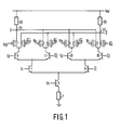
- Fig. 1 is a circuit diagram of a programmable BiMOS combinational logic circuit in accordance with the invention;
- Fig. 2 is a preferred modification of the circuit in Fig. 1;
- Fig. 3 is a level shifting arrangement for adjusting the DC level of the signal inputs to the logic circuit in Fig. 1 or 2 to avoid saturation of the bipolar transistors therein; and
- Fig. 4 is a circuit diagram of a programmable CMOS combinational logic circuit in accordance with the invention.
- Referring to Fig. 1, there is shown a logic circuit in accordance with the invention which is programmable to provide any selected combinational logic function of a plurality, in this case two, logic signals S1 and S2. The resulting output signal Q, and preferably also its complement Q, are produced at respective output terminals of the circuit.
- The circuit can be readily extended for any number of input logic signals, there being a respective gating level for each such signal. Each gating level includes one or more pairs of logic switches, which in the embodiment in Fig. 1 are in the form of NPN bipolar transistors which each have a control terminal, a first current terminal, and a second current terminal. More specifically, the control terminal is at the base and the first and second current terminals are respectively at the emitter and collector. It will be obvious that with appropriate changes of polarity of the various signals and power supply voltages PNP transistors could equally well be employed.
- The first logic signal S1 and its complement"S1 are respectively supplied to the control terminals, i.e. the bases of a pair of
transistors 1 and 3 in the first gating level of the circuit. It will be obvious that in lieu of employing NPN bipolar transistors the same results could be achieved using PNP transistors instead, with reversal of all voltage polarities. For simplicity of description, however, it will be assumed hereinafter that all of the bipolar transistors in Fig. 1 are NPN transistors. - The emitters of
transistors 1 and 3 are connected in common to a constant current source which may conveniently be an NPN transistor 5 in series with aresistor 7 which is connected to ground, the base of transistor 5 being supplied with a constant bias voltage Vb which results in adequate collector current so that thetransistors - The second gating level of the circuit in Fig. 1 receives the second logic signal S2 and comprises two pairs of bipolar NPN transistors; a
first pair 9 and 11 the emitters of which are connected in common to the collector of transistor 1 in the first gating level, and asecond pair transistor 3 in the first gating level. The second input signal S2 and its complement S2 are respectively supplied to the bases oftransistors 9 and 11 in the first pair and also to the bases oftransistors transistors - It will be apparent from the foregoing description that the logic circuit has the form of a branching tree structure of successive serially interconnected gating levels, each level being for a respective input logic signal. For (L) such signals there would be (L) gating levels, any nth level having 2n-1 pairs of logic switches.
- Alternatively to using signals S1 and S2, complementary to the signals S1 and S2, the input signals at the control terminals of the
relevant transistors - Programming of the logic circuit is provided by a programming level thereof which is coupled to the highest gating level and includes respective pairs of logic switches for the respective logic switches in the highest gating level. Each pair of logic switches in the programming level has at least one control terminal for receiving a logic programming signal, a first current terminal which is coupled to the collector of a respective transistor in the highest gating level, and a pair of second current terminals which are separately coupled to a supply voltage line Vdd via
resistors bipolar transistor 9 in the second gating level; a second pair of Pchannel MOS transistors channel MOS transistors transistor 13 in the second gating levels; and a fourth pair of Pchannel MOS transistors transistor 15 in the second gating level. The sources of each of the aforesaid pairs of MOS transistors constitute the above-referred to pair of second current terminals of each such pair. - A first programming signal goo and its complement goo are respectively applied to the gates of the first pair of programming switch MOS transistors 17 and 19, a second programming signal go and its complement 901 are respectively applied to the gates of the second pair of programming
switch MOS transistors switch MOS transistors 25ad 27, ad a fourth programming signal g11 and its complementg 11 are respectively applied to the gates of the fourth pair of programmingswitch MOS transistors junction point 33 which is coupled via a path including aresistor 35 to the positive voltage supply rail Vdd. The output signal Q of the logic circuit is thereby available atjunction point 33. The sources of those of the programming switch MOS transistors which receive complemented programming signals at their gates are all connected in common to ajunction point 37 which is coupled via a path including aresistor 39 to the positive voltage supply rail Vdd, and a complemented output signal Q of the logic circuit is available atjunction point 37. - Fig. 2 is a modified form of the circuit of Fig. 1 which further enhances the speed of operation. The layout and operation of the circuit is largely identical to that in Fig. 1, corresponding elements thereof having the same identifying numerals. The improvement over the circuit of Fig. 1 is that a
bipolar transistor 41 is included in cascode connection betweenjunction 33ad resistor 35, and similarly abipolar transistor 43 is connected in cascode connection betweenjunction point 37 andresistor 39. More specifically, the emitter oftransistor 41 is connected tojunction point 33 and the collector thereof is connected toresistor 35, and the emitter oftransistor 43 is connected tojunction point 37 and the collector thereof is connected toresistor 39. The bases oftransistors transistors - The presence of a constant current source, formed by the transistor 5 and the
resistor 7, further avoids saturation effects in the layer of transistors connected closest to the voltage supply line Vdd, whether these are the programming switches 17 to 31 as in Fig. 1, or thecascode transistors - The programming signals for implementing a selected combinational logic function of the input signals S1 and S2 may typically be obtained from a CMOS static memory wherein such signals are stored at respective addresses. Consequently, the programming signals will be enumerated herein as if they were binary addresses in such a memory. It will be noted that with (L) logic signals there will be (L) gating levels, any nth gating level having 2n logic switches and so 2n control terminals. Consequently, to cover all possible
combinational logic functions 2L programming signals will be required. That can be achieved, as shown in Fig. 1, by providing 2L programming signals along with the complements thereof. However, an equally suitable alternative would be to provide only non-complemented programming signals and to use complementary MOS transistors (CMOS-logic) in each pair of transistors which constitute the pairs of logic switches in the programming level of the logic circuit. Such a modification will be obvious to those skilled in the art. - The operation of the logic circuit in Fig. 1 will now be described. If the input logic signals S1 and S2 are both high (i.e., a logic "1 ") transistor 1 in the first gating level and
transistor 9 coupled thereto in the second gating level will both be in the conductive or "on" state.Transistors 3 and 11 will be "off". Astransistor 3 is "off", the state oftransistors junction point 37 andtransistor 43 tooutput load resistor 39, and so the voltage at thecollector transistor 43, which constitutes the complemented output signalQ , will be low or "0". The non-complemented output signal Q at the collector oftransistor 41 will be high, because since programming MOS transistor 17 is off there will be no current path throughresistor 35. If, on the other hand, the programming signal goo is low, its complement goo being high, the situation will be reversed and a current path will be established by transistor 17 viajunction point 33,transistor 41 andload resistor 35 to the Vdd supply rail. The output signal Q will therefore be low and the complemented output signalQ will be high. The logic function established by programming signal goo can therefore be expressed as

- A similar analysis applies to the remaining three pairs of programming MOS transistors and the programming signals applied thereto, so that the complete logic functions established by output signals Q and Q can be expressed as


- Since the logic value of an input logic signal can only be either "1" " or "0", each term in equation (1) can be generically expressed as

where ⊕ is the exclusive OR symbol and effectively serves to invert the associated S1 or S2 term when "i" or "j" is "1". The same is true for equation "2", except that gij is inverted tog ij. For example, if i and j are both "O, the above expression becomes goo.S1.S2, which is the first term in equation (1). If i = O and j = 1 the above expression becomes g01.S1.S 2, which is the second term in equation (1). The same relationships also apply to the remaining terms in equation (1). In general, for any number n of input logic signals in1, in2,...inn there will be 2n programming signals of the form giik...n. Consequently, equation (1) can be expressed as
- Referring back to equations (1) and (2), it is apparent therefrom that by appropriate choice of the programming signals gij, it is possible to implement all possible combinational logic functions of the input logic signals. For example, if the only non-complemented programming signal which is high is goo, equation (1) becomes Q = S1.S2 and so at the Q output the circuit functions as an AND gate. If the only complemented programming signal which is high is
g 11 equation (2) becomes Q = S, .S2, which is equivalent to Q = S1 + S2. Therefore, at the Q output the circuit functions as a OR gate. A NOR operation will be obtained at the Q output, as seen from equation (1), when the only non-complemented programming signal which is high is g11. An XOR operation which can be expressed as (S1.S 2) + (S 1.S2), will be provided at the Q output when, as seen from equation (2), the only complemented programming signals which are high are go and gio. More combinations and logic functions can be composed. With two input logic signals and four programming signals a total of sixteen combinations is possible. Several of these combinations are functionally identical. - The logic circuit of Fig. 1 can be employed as a prototype for a final version thereof to be included in a complete PLD, since it can be easily programmed and reprogrammed, even during operation, while debugging of the complete device is carried out. Eprom transistors or possibly fusible links can then be substituted for the programming switches. This mode of design makes it possible to significantly reduce the production cost of the final device.
- To prevent saturation of the bipolar transistors the dc level of the input logic signals S1 and S2 should be within predetermined limits. That can be achieved by providing a level shifter for each of the input logic signals and using the outputs of such level shifters as the actual logic signals which are input to the gating circuit. Such level shifters are well known, one example being shown in Fig. 3. Therein there are two diode- connected bipolar transistors in series between a
bipolar transistor 45, the collector of which is connected to Vdd, and a current level settingbipolar transistor 47 which is supplied with a fixed base bias voltage Vb. The emitter oftransistor 47 is returned to ground by aresistor 49. The input logic signal Vin is supplied to thebase transistor 45. The corresponding output signal can be taken at the emitter of any of such transistors, except thecurrent source transistor 47, and will be equal to Vin less a number of base-emitter voltage drops Vbe equal to the number of transistors up to and including that at which the output is taken. - Although the programmable logic circuit of Fig. 1 provides high speed operation by virtue of its BiMOS construction, the novel features thereof can also be implemented at lower cost entirely in CMOS if somewhat lower speed is acceptable. In that case, no level shifters will be required because the logic input signals will all be voltage swings from ground potential to Vdd. This embodiment of the invention is shown in Fig. 4.
- As in the BiMOS logic circuit of Fig. 1, the CMOS logic circuit in Fig. 4 has respective gating levels for the respective input logic signals. The first gating level has one pair of
switches S 1. The second gating level has two pairs of such logic switches, the first current terminals of each such pair being connected together and to the second current terminal of one of the logic switches in the first gating level. The first control terminals of each such pair receive the input logic signal S2, and the second control terminals of each such pair receive the complement logic signal S2. - More specifically, each logic switch consists of a pair of CMOS transistors connected in parallel, the sources thereof being connected together to constitute a first current terminal and the drains thereof being connected together to constitute a second current terminal, thereby forming two oppositely directed transmission paths, one direction for producing the non-complemented Q output signal of the gate circuit and the other direction for producing the complemented Q output signal. In the first gating level of the circuit, the
logic switch 54 includes Pchannel MOS transistor 51 and Nchannel MOS transistor 53, and thelogic switch 58 includes P channel MOS transistor 55 and Nchannel MOS transistor 57. The common drain connections of both of such switches are connected to anoutput terminal 59, at which the Q output signal of the logic circuit is produced. Aninverter 60 coupled toterminal 59 provides the non-complemented output signal Q. - The second gating level of the logic circuit in Fig. 3 comprises two pairs of logic switches, one
pair being switches switches CMOS transistors logic switch 54 in the first gating level, the latter connection constituting the second current terminal oflogic switch 54. - The common drain connections of the
switch pair CMOS transistors 55 and 57 oflogic switch 58 in the third gating level, the latter connection constituting the second current terminal oflogic switch 58. The common source connections of the respective logic switches 60, 61, 62 and 63, which constitute the second current terminals thereof, are respectively connected to the first current terminals of therespective CMOS gates - The first logic input signal S1, which controls the first gating level, is supplied to the gate of
N channel transistor 53 inlogic gate 54 and also to the gate of P channel transistor 55 inlogic gate 58. The complement"S1 of such input signal is supplied to the gates of the remainingcomplementary transistors logic gates logic gates - To comprehend the operation of the logic circuit in Fig. 3, it will be recalled that conduction between the source and drain of an N channel transistor requires that the gate thereof be positive relative to the source whereas conduction between the source and drain of a P channel transistor requires that the gate thereof be negative relative to the source. Consequently, a programming signal which is high (or I) can only render the N channel transistors of the relevant logic switches in the programming level conductive, whereas a low or "O" programming signal can only render the P channel transistors of such logic switches conductive. Similarly, an N channel transistor of a logic switch in the gating level will conduct in response to a "1" " logic signal at the gate thereof if its source is at the "O" signal level, and the P channel transistor of such logic switch will conduct in response to a "O" logic signal at the gate thereof if its source is at the "1" signal level. Consequently, the N channel transistor in the logic switches in the programming and gating levels establish conduction paths by which a "1" " programming signal can produce a "O"
signal terminal 59, and the P channel transistors establish conduction paths by which a "O" programming signal can produce a "1" " signal atterminal 59. - Considering the goo programming signal, for example, if it is a "1" it it will turn on the N channel transistor in
programming switch 64, and since the source of such transistor is connected to ground a "O" will be produced at the drain thereof. Such "O" is thereby supplied to the second current terminal ofswitch 60 in the second gating level, and thus to the sources of the transistors therein. If the input signal S2 is "1", the N channel transistor inswitch 60 will therefore conduct and produce a "O" at the drain thereof and so at the first current terminal ofswitch 60. A "O" is thereby applied to the second current terminal oflogic switch 54 in the first gating level. If the input signal S1 is "1", the "0" at the source at the N channel transistor inswitch 54 will be conveyed to the drain thereof and so to the first current terminal ofswitch 54. A "O" will therefore be produced atterminal 59, and so the logic circuit produces a Q = output signal. Applying the foregoing analysis for the situation in which the goo programming signal is a "0", a "1" " will be supplied to the second current terminal oflogic switch 60. If, as before, the logic signals Si and S2 are both "1 ", so that S1 and S2 are both "0", a "1" " will be produced atterminal 59 and so the logic circuit then produces a Q output signal. The circuit operation is therefore in accordance with the following logic functions:

- Comparing this with equations (1) and (2) above, it is in conformity therewith. Consequently, it will be apparent that the circuit in Fig. 3 provides the same combinational logic functions as those of the circuit in Fig. 1 as described above. The Q output is determined entirely by non-complemented programming signals which are high, and the Q output is determined entirely by complemented programming signals which are high. Since all programming signals in Fig. 3 are rail-to-rail swings between Vdd and ground, no level shifters are necessary.
- It should be understood that as used herein the term MOS transistor signifies any type of insulated gate field effect transistor, and not necessarily one in which the gate is a metal on oxide arrangement. In addition, while the invention has been described with reference to certain preferred embodiments, it will be apparent to those skilled in the art that various adaptations and extensions thereof can be made without departing from the essential teachings and scope of the invention as set forth in the ensuing claims.
Claims (6)
1. A programmable logic circuit for deriving any selected combinational logic function of plurality of logic signals which are input thereto, said logic circuit comprising: a succession of serially interconnected gating levels, each for a respective input logic signal and each including one or more pairs of logic gating switches, each such gating switch having a first current terminal and a second current terminal and at least one control terminal for receiving the input logic signal for the relevant gating level, each gating switch being adapted to establish or break a conductive connection between its current terminals depending on the logic value of the logic signal at its control terminal; the second current terminal of each gating switch in any given gating level being coupled in common to both of the first current terminals of a pair of gating switches in the next higher gating level, thereby forming a branching tree structure wherein each successive gating level has twice as many pairs of gating switches as the preceding gating level; and a programming level coupled to the highest gating level of said tree structure and which includes respective pairs of logic switches for respective programming signals; each such logic programming switch having a control terminal for receiving a programming signal, a first current terminal and a second current terminal, and being adapted to establish or break a connection between said current terminals depending on the logic value of the programming signal at its control terminal; the pair of first current terminals of each respective pair of programming switches being coupled in common to the second current terminal of a respective gating switch in the highest gating level of said logic circuit.
2. A programmable logic circuit as claimed in claim 1, wherein: each of said gating switches is a bipolar transistor having an emitter which constitutes one of said first and second current terminals of such gating switch, a collector which constitutes the other of said second current terminals, and a base which constitutes a control terminal of such gatinswitch; each of said programming switches is a field effect transistor having a source which constitutes one of said current terminals of such programming switch, a drain which constitutes the other of said current terminals, and a gate which constitutes the control terminal of such programming switch; the first gating level of said logic circuit includes a single pair of gating switches, the first current terminals thereof being connected in common to a source of substantially constant current; and corresponding ones of the second current terminals Oc all of said pairs of programming switches are coupled to a common connection terminal which constitutes an output terminal of said logic circuit; whereby said logic circuit produces at said output terminal a signal which constitutes a combinational logic function of all of said input logic signals, such combinational logic function being determined by the logic values of said programming signals.
3. A programmable logic circuit as claimed in claim 1, wherein: each of said gating switches is a CMOS pair of field effect transistors the sources of which are connected together to constitute one of said first and second current terminals of such gating switch and the drains of which are connected together to constitute the other of said current terminals, the gates of said field effect transistors constituting the control terminals of such gating switch; each of said programming switches is a field effect transistor, the pair of transistors which constitutes any of said pairs of programming switches being complementary; the source of each such transistor constituting one of said first and second current terminals of the relevant programming switch and the drain of such transistor constituting the other of said current terminals; programming signals for any given pair of programming switches are received at the gates of the transistors which constitute such pair of programming switches, the second current terminals of said pair of transistors being respectively connected to reference potential and to a source of supply potential; and the first gating level of said logic circuit includes a single pair of gating switches, the first current terminals of such pair of gating switches being coupled together to a common connection terminal, such common connection terminal constituting an output terminal of said logic circuit; whereby said logic circuit produces at said output terminal an output signal which is a combinational logic function of all of said input logic signals, such combinational logic function being determined by the logic values of said programming signals.
4. A programmable logic circuit for deriving any selected combinational logic function of a plurality of logic signals which are input thereto, said logic circuit comprising: a succession of serially interconnected gating levels, each for a respective input logic signal and each including one or more pairs of bipolar transistors, each of said transistors have a base, a first current terminal and a second current terminal; the first gating level comprising one of said pairs of bipolar transistors, said transistors respectively receiving at their bases a first of said input logic signals and the complement thereof; any nth gating level comprising 2n-1 of said pairs of bipolar transistors, the transistors in each such pair respectively receiving at their bases the nth logic signal and the complement thereof, the first current terminals of the transistors in each such pair being connected in common to the second current terminal of a respective transistor in the (n-1)st gating level; a programming level following the highest (L)th gating level and which includes 2L pairs of field effect transistors (FETs), each FET having a gate and a first and second current terminal, each such pair of FETs respectively receiving at the gates thereof a respective programming signal and its complement, the first current terminals of each such pair being connected in common to the second current terminal of a respective one of the transistors in the Lth gating level; and circuit means coupled in common to the second current terminal of one of the FETs in each of said 2L pairs of FETs in said programming level for providing a logic output signal from said gate circuit, said output signal being a combinational logic function of all of said input logic signals, such combinational logic function being determined by the logic values of said programming signals.
5. A programmable logic circuit as claimed in claim 4, wherein one of the second current terminals of each of said pairs of FETs in the programming level are connected to a common connection terminal, and said circuit means comprises an output bipolar transistor having its emitter and collector connected in cascode between a source of supply voltage and said common connection terminal, said output signal being produced at the collector of said output bipolar transistor.
6. A programmable logic circuit for deriving of any selected combinational logic function of a plurality n (n > 2) of logic signals which are input thereto, said logic circuit comprising: a succession of serially interconnected gating levels, each for a respective input logic signal and each including one or more pairs of logic switches; each such gating switch having a first and a second current terminal and including a pair of CMOS transistors the drains of which are both connected to one of said current terminals and the sources of which are both connected to the other of said current terminals, the gates of said CMOS transistors of a gating switch in any gating level respectively receiving the logic signal for that level and the complement thereof, the first gating level comprising one pair of said gating switches and any nth gating level comprising 2n-' pairs of said gating switches; the first current terminals of each pair of gating switches in any gating level above the first gating level being connected in common to the second current terminal of one of the gating switches in the preceding gating level, the first current terminals of the pair of gating switches in the first gating level being connected together to a terminal which is an output terminal of said logic circuit; and a programming level following the highest (L)th gating level and which includes 2L pairs of programming switches, each such programming switch having a first current terminal and a second current terminal and including a field effect transistor (FET), the source of the FET of a programming switch being connected to one of the current terminals of such programming switch and the drain of such FET being connected to the other of said current terminals, the FETs in each pair of programming switches being complementary; each respective pair of programming switches receiving a respective programming signal at the gates of the FETs therein, the first current terminals of such pair of programming switches being connected in common to the second current terminal of a gating switch in said (L)th gating level, and the second current terminals of such pair of programming switches being respectively connected to reference potential and a source of supply potential.
Applications Claiming Priority (2)
| Application Number | Priority Date | Filing Date | Title |
|---|---|---|---|
| US695036 | 1985-01-25 | ||
| US07/695,036 US5124588A (en) | 1991-05-01 | 1991-05-01 | Programmable combinational logic circuit |
Publications (2)
| Publication Number | Publication Date |
|---|---|
| EP0511711A2 true EP0511711A2 (en) | 1992-11-04 |
| EP0511711A3 EP0511711A3 (en) | 1995-03-15 |
Family
ID=24791289
Family Applications (1)
| Application Number | Title | Priority Date | Filing Date |
|---|---|---|---|
| EP92201158A Withdrawn EP0511711A3 (en) | 1991-05-01 | 1992-04-24 | Programmable combinational logic circuit |
Country Status (3)
| Country | Link |
|---|---|
| US (1) | US5124588A (en) |
| EP (1) | EP0511711A3 (en) |
| JP (1) | JPH05145405A (en) |
Cited By (2)
| Publication number | Priority date | Publication date | Assignee | Title |
|---|---|---|---|---|
| EP0898370A1 (en) * | 1997-08-19 | 1999-02-24 | Hewlett-Packard Company | Differential CMOS logic family |
| FR2792475A1 (en) * | 1999-04-16 | 2000-10-20 | St Microelectronics Sa | Comparator for digital value bits at CMOS voltage levels and bit with digital value at ECL voltage levels |
Families Citing this family (13)
| Publication number | Priority date | Publication date | Assignee | Title |
|---|---|---|---|---|
| US5686791A (en) | 1992-03-16 | 1997-11-11 | Microelectronics And Computer Technology Corp. | Amorphic diamond film flat field emission cathode |
| FR2724073A1 (en) * | 1994-08-31 | 1996-03-01 | Sgs Thomson Microelectronics | LOGIC CIRCUIT WITH DIFFERENTIAL STAGES |
| JP2728013B2 (en) * | 1995-03-10 | 1998-03-18 | 日本電気株式会社 | BiCMOS logic gate circuit |
| WO1997047088A1 (en) * | 1996-06-04 | 1997-12-11 | Hitachi, Ltd. | Semiconductor integrated circuit |
| GB2318665B (en) * | 1996-10-28 | 2000-06-28 | Altera Corp | Work group computing for electronic design automation |
| US6286114B1 (en) * | 1997-10-27 | 2001-09-04 | Altera Corporation | Enhanced embedded logic analyzer |
| US6408501B1 (en) | 1998-07-30 | 2002-06-25 | Central Corporation | Automatic system of manufacturing ball studs for vehicles |
| US6754862B1 (en) | 2000-03-09 | 2004-06-22 | Altera Corporation | Gaining access to internal nodes in a PLD |
| US7036046B2 (en) * | 2002-11-14 | 2006-04-25 | Altera Corporation | PLD debugging hub |
| US7076751B1 (en) | 2003-01-24 | 2006-07-11 | Altera Corporation | Chip debugging using incremental recompilation |
| US7539900B1 (en) | 2003-07-29 | 2009-05-26 | Altera Corporation | Embedded microprocessor for integrated circuit testing and debugging |
| US7206967B1 (en) | 2004-02-09 | 2007-04-17 | Altera Corporation | Chip debugging using incremental recompilation and register insertion |
| US8296604B1 (en) * | 2009-10-12 | 2012-10-23 | Xilinx, Inc. | Method of and circuit for providing temporal redundancy for a hardware circuit |
Citations (7)
| Publication number | Priority date | Publication date | Assignee | Title |
|---|---|---|---|---|
| US3691401A (en) * | 1971-03-10 | 1972-09-12 | Honeywell Inf Systems | Convertible nand/nor gate |
| US4069426A (en) * | 1975-10-06 | 1978-01-17 | Tokyo Shibaura Electric Co., Ltd. | Complementary MOS logic circuit |
| JPS59208943A (en) * | 1983-05-12 | 1984-11-27 | Matsushita Electric Ind Co Ltd | Logical circuit |
| GB2146863A (en) * | 1983-09-15 | 1985-04-24 | Ferranti Plc | Bipolar transistor logic circuits |
| JPS60113525A (en) * | 1983-11-24 | 1985-06-20 | Sharp Corp | Ecl gate circuit |
| JPS6165623A (en) * | 1984-09-07 | 1986-04-04 | Nippon Telegr & Teleph Corp <Ntt> | Cmos selector circuit |
| EP0187697A2 (en) * | 1985-01-04 | 1986-07-16 | Advanced Micro Devices, Inc. | Balanced CMOS logic circuits |
Family Cites Families (7)
| Publication number | Priority date | Publication date | Assignee | Title |
|---|---|---|---|---|
| JPS6018892A (en) * | 1983-07-12 | 1985-01-30 | Sharp Corp | Semiconductor decoding circuit |
| KR920011006B1 (en) * | 1983-08-22 | 1992-12-26 | 가부시끼가이샤 히다찌세이사꾸쇼 | Semiconductor integrated circuit device |
| FR2581811A1 (en) * | 1985-05-10 | 1986-11-14 | Radiotechnique Compelec | NUMERIC MULTIPLEXER MODULE WITH N INPUTS AND MULTIPLEXER WITH N2 INPUTS INCORPORATING SUCH MODULES |
| US4754173A (en) * | 1985-06-13 | 1988-06-28 | Digital Equipment Corporation | Emitter coupled logic latch with boolean logic input gating network |
| US4713560A (en) * | 1986-06-05 | 1987-12-15 | Fairchild Semiconductor Corporation | Switched impedance emitter coupled logic gate |
| US4963767A (en) * | 1988-08-25 | 1990-10-16 | National Semiconductor Corporation | Two-level ECL multiplexer without emitter dotting |
| DE3883389T2 (en) * | 1988-10-28 | 1994-03-17 | Ibm | Two-stage address decoding circuit for semiconductor memories. |
-
1991
- 1991-05-01 US US07/695,036 patent/US5124588A/en not_active Expired - Fee Related
-
1992
- 1992-04-24 EP EP92201158A patent/EP0511711A3/en not_active Withdrawn
- 1992-04-30 JP JP4111769A patent/JPH05145405A/en active Pending
Patent Citations (7)
| Publication number | Priority date | Publication date | Assignee | Title |
|---|---|---|---|---|
| US3691401A (en) * | 1971-03-10 | 1972-09-12 | Honeywell Inf Systems | Convertible nand/nor gate |
| US4069426A (en) * | 1975-10-06 | 1978-01-17 | Tokyo Shibaura Electric Co., Ltd. | Complementary MOS logic circuit |
| JPS59208943A (en) * | 1983-05-12 | 1984-11-27 | Matsushita Electric Ind Co Ltd | Logical circuit |
| GB2146863A (en) * | 1983-09-15 | 1985-04-24 | Ferranti Plc | Bipolar transistor logic circuits |
| JPS60113525A (en) * | 1983-11-24 | 1985-06-20 | Sharp Corp | Ecl gate circuit |
| JPS6165623A (en) * | 1984-09-07 | 1986-04-04 | Nippon Telegr & Teleph Corp <Ntt> | Cmos selector circuit |
| EP0187697A2 (en) * | 1985-01-04 | 1986-07-16 | Advanced Micro Devices, Inc. | Balanced CMOS logic circuits |
Non-Patent Citations (6)
| Title |
|---|
| IBM TECHNICAL DISCLOSURE BULLETIN, vol.26, no.7A, December 1983 pages 3515 - 3517 J. W. DAVIS ET AL.: 'Sixteen-input funnel utilizing five-level differential cascode current switch' * |
| IEEE JOURNAL OF SOLID-STATE CIRCUITS, vol.24, no.5, October 1989, NEW YORK, US pages 1265 - 1270 M. INO ET AL.: '30-ps 7.5-GHz GaAs MESFET Macrocell Array' * |
| PATENT ABSTRACTS OF JAPAN vol. 10, no. 233 (E-427) (2289) 13 August 1986 & JP-A-61 065 623 (NIPPON TELEGR & TELEPH CORP <NTT>) * |
| PATENT ABSTRACTS OF JAPAN vol. 9, no. 266 (E-352) (1989) 23 October 1985 & JP-A-60 113 525 (SHARP K. K.) 20 June 1985 * |
| PATENT ABSTRACTS OF JAPAN vol. 9, no. 75 (E-306) (1798) 4 April 1985 & JP-A-59 208 943 (MATSUSHITA DENKI SANGYO K. K.) 27 November 1984 * |
| RADIO FERNSEHEN ELEKTRONIK, vol.26, no.1, January 1977 pages 10 - 24 M. AUER ET AL.: 'Komplexe ECL-Schaltkreise' * |
Cited By (4)
| Publication number | Priority date | Publication date | Assignee | Title |
|---|---|---|---|---|
| EP0898370A1 (en) * | 1997-08-19 | 1999-02-24 | Hewlett-Packard Company | Differential CMOS logic family |
| US6008670A (en) * | 1997-08-19 | 1999-12-28 | Hewlett-Packard | Differential CMOS logic family |
| FR2792475A1 (en) * | 1999-04-16 | 2000-10-20 | St Microelectronics Sa | Comparator for digital value bits at CMOS voltage levels and bit with digital value at ECL voltage levels |
| US6335677B1 (en) | 1999-04-16 | 2002-01-01 | Stmicroelectronics S.A. | Comparator of a digital value having CMOS voltage levels with a digital value having ECL voltage levels |
Also Published As
| Publication number | Publication date |
|---|---|
| JPH05145405A (en) | 1993-06-11 |
| US5124588A (en) | 1992-06-23 |
| EP0511711A3 (en) | 1995-03-15 |
Similar Documents
| Publication | Publication Date | Title |
|---|---|---|
| US5124588A (en) | Programmable combinational logic circuit | |
| US7046041B1 (en) | Structures and methods of implementing a pass gate multiplexer with pseudo-differential input signals | |
| US4575648A (en) | Complementary field effect transistor EXCLUSIVE OR logic gates | |
| US5656948A (en) | Null convention threshold gate | |
| KR900003070B1 (en) | Logic circuit | |
| US4041326A (en) | High speed complementary output exclusive OR/NOR circuit | |
| US3551693A (en) | Clock logic circuits | |
| US5909127A (en) | Circuits with dynamically biased active loads | |
| JPH06169252A (en) | Programmable logic-circuit device | |
| US4408134A (en) | Unitary exclusive or-and logic circuit | |
| US4091293A (en) | Majority decision logic circuit | |
| EP0085569A2 (en) | Gallium arsenide logic circuit | |
| US5909187A (en) | Current steering circuit for a digital-to-analog converter | |
| KR890015425A (en) | Semiconductor integrated circuit using bipolar transistor and CMOS transistor | |
| US5664211A (en) | Null convention threshold gate | |
| US3660678A (en) | Basic ternary logic circuits | |
| US4943740A (en) | Ultra fast logic | |
| US4801819A (en) | Clocked CMOS circuit with at least one CMOS switch | |
| KR930004351B1 (en) | Level shift circuit | |
| US3430071A (en) | Logic circuit | |
| US5198704A (en) | Bi-CMOS output circuit with limited output voltage | |
| KR890008999A (en) | Digital integrated circuits | |
| US6255857B1 (en) | Signal level shifting circuits | |
| US6072413A (en) | Current output type digital-to-analog converter capable of suppressing output current fluctuation using a current mirror | |
| US4977338A (en) | High speed bipolar-MOS logic circuit including a series coupled arrangement of a bipolar transistor and a logic block having a MOSFET |
Legal Events
| Date | Code | Title | Description |
|---|---|---|---|
| PUAI | Public reference made under article 153(3) epc to a published international application that has entered the european phase |
Free format text: ORIGINAL CODE: 0009012 |
|
| AK | Designated contracting states |
Kind code of ref document: A2 Designated state(s): DE FR GB IT |
|
| PUAL | Search report despatched |
Free format text: ORIGINAL CODE: 0009013 |
|
| AK | Designated contracting states |
Kind code of ref document: A3 Designated state(s): DE FR GB IT |
|
| 17P | Request for examination filed |
Effective date: 19950915 |
|
| STAA | Information on the status of an ep patent application or granted ep patent |
Free format text: STATUS: THE APPLICATION HAS BEEN WITHDRAWN |
|
| 18W | Application withdrawn |
Withdrawal date: 19960409 |