EP0497097A2 - Switching system with time-stamped packet distribution input stage and packet sequencing output stage - Google Patents
Switching system with time-stamped packet distribution input stage and packet sequencing output stage Download PDFInfo
- Publication number
- EP0497097A2 EP0497097A2 EP92100201A EP92100201A EP0497097A2 EP 0497097 A2 EP0497097 A2 EP 0497097A2 EP 92100201 A EP92100201 A EP 92100201A EP 92100201 A EP92100201 A EP 92100201A EP 0497097 A2 EP0497097 A2 EP 0497097A2
- Authority
- EP
- European Patent Office
- Prior art keywords
- packet
- packets
- timeslot
- timeslot number
- output
- Prior art date
- Legal status (The legal status is an assumption and is not a legal conclusion. Google has not performed a legal analysis and makes no representation as to the accuracy of the status listed.)
- Granted
Links
Images


Classifications
-
- H—ELECTRICITY
- H04—ELECTRIC COMMUNICATION TECHNIQUE
- H04L—TRANSMISSION OF DIGITAL INFORMATION, e.g. TELEGRAPHIC COMMUNICATION
- H04L49/00—Packet switching elements
- H04L49/15—Interconnection of switching modules
- H04L49/1515—Non-blocking multistage, e.g. Clos
- H04L49/153—ATM switching fabrics having parallel switch planes
- H04L49/1538—Cell slicing
-
- H—ELECTRICITY
- H04—ELECTRIC COMMUNICATION TECHNIQUE
- H04L—TRANSMISSION OF DIGITAL INFORMATION, e.g. TELEGRAPHIC COMMUNICATION
- H04L49/00—Packet switching elements
- H04L49/15—Interconnection of switching modules
- H04L49/1553—Interconnection of ATM switching modules, e.g. ATM switching fabrics
-
- H—ELECTRICITY
- H04—ELECTRIC COMMUNICATION TECHNIQUE
- H04L—TRANSMISSION OF DIGITAL INFORMATION, e.g. TELEGRAPHIC COMMUNICATION
- H04L49/00—Packet switching elements
- H04L49/30—Peripheral units, e.g. input or output ports
-
- H—ELECTRICITY
- H04—ELECTRIC COMMUNICATION TECHNIQUE
- H04L—TRANSMISSION OF DIGITAL INFORMATION, e.g. TELEGRAPHIC COMMUNICATION
- H04L49/00—Packet switching elements
- H04L49/30—Peripheral units, e.g. input or output ports
- H04L49/3081—ATM peripheral units, e.g. policing, insertion or extraction
-
- H—ELECTRICITY
- H04—ELECTRIC COMMUNICATION TECHNIQUE
- H04L—TRANSMISSION OF DIGITAL INFORMATION, e.g. TELEGRAPHIC COMMUNICATION
- H04L12/00—Data switching networks
- H04L12/54—Store-and-forward switching systems
- H04L12/56—Packet switching systems
- H04L12/5601—Transfer mode dependent, e.g. ATM
- H04L2012/5638—Services, e.g. multimedia, GOS, QOS
- H04L2012/5646—Cell characteristics, e.g. loss, delay, jitter, sequence integrity
- H04L2012/565—Sequence integrity
-
- H—ELECTRICITY
- H04—ELECTRIC COMMUNICATION TECHNIQUE
- H04L—TRANSMISSION OF DIGITAL INFORMATION, e.g. TELEGRAPHIC COMMUNICATION
- H04L49/00—Packet switching elements
- H04L49/20—Support for services
-
- H—ELECTRICITY
- H04—ELECTRIC COMMUNICATION TECHNIQUE
- H04L—TRANSMISSION OF DIGITAL INFORMATION, e.g. TELEGRAPHIC COMMUNICATION
- H04L49/00—Packet switching elements
- H04L49/30—Peripheral units, e.g. input or output ports
- H04L49/3009—Header conversion, routing tables or routing tags
-
- H—ELECTRICITY
- H04—ELECTRIC COMMUNICATION TECHNIQUE
- H04L—TRANSMISSION OF DIGITAL INFORMATION, e.g. TELEGRAPHIC COMMUNICATION
- H04L49/00—Packet switching elements
- H04L49/50—Overload detection or protection within a single switching element
- H04L49/501—Overload detection
- H04L49/503—Policing
Definitions
- the present invention relates generally to packet switching systems, and more specifically to a fast packet switching system for ISDN (Integrated Services Digital Network).
- ISDN Integrated Services Digital Network
- the switching speed of the prior art packet switching systems is given by the relation N x V/K, where V is the line transmission speed, N the number of input ports, and K the number of packet segments into which each packet is bit-sliced.
- V the line transmission speed
- N the number of input ports
- K the number of packet segments into which each packet is bit-sliced.
- the line speed and the number of input ports can be increased by increasing the K value whose maximum value is equal to the bit length L.
- a packet switching system having a plurality of input ports and a plurality of output ports.
- the system comprises a plurality of packet distributers associated respectively with the input ports for receiving successive packets therefrom, each of the packet distributers attaching a timeslot number to each of the received packets, and uniformly distributing the packets to a plurality of output terminals thereof.
- a plurality of packet switches comprise the center stage of the system. These packet switches correspond in number to the output terminals of each of the packet distributers, and each of the packet switches has a plurality of input terminals corresponding in number to the packet distributers and a plurality of output terminals corresponding in number to the output ports.
- each packet switch is coupled to respective output terminals of the packet distributers for switching a packet from one of the input terminals thereof to one of the output terminals thereof in accordance with a destination address contained in the packet.
- a plurality of packet sequencers are associated respectively with the output ports.
- Each of the packet sequencers has a plurality of input terminals coupled to respective output terminals of the packet switches for examining the timeslot numbers attached to packets from the input terminals thereof and delivering the packets to the associated output port in accordance with the examined timeslot numbers.
- each of the packet switches For uniform distribution of packets to the center stage, each of the packet switches generates a traffic-related signal indicating the amount of packets outstanding in the packet switch.
- Each packet distributer receives the traffic-related signal from each packet switch and gives priority to the output terminals of the packet distributer according to the amounts of packets outstanding in the respective packet switches. In this way, packets from the associated input port are distributed with priority to those of the packet switches containing a smaller amount of outstanding packets.
- bit-slicing technique can be used for higher speed switching application. If bit-slicing technique is used for the center switching stage, the switching speed of the system can be decreased to N x V/P x L, where P is the number of switches of the center stage.
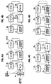
- the switching system has four input ports 101 through 104 for receiving packets of a predetermined bit length from user stations at a line clock rate specified by the system and switching the received packets to one of four output ports 141 through 144.
- Each packet contains a label indicating a destination user station.
- the system comprises a plurality of packet distributers 111 ⁇ 114 corresponding respectively to the input ports 101 ⁇ 104, a plurality of 4 x 4 self-routing packet switches 121 - 124 corresponding in number to the packet distributers, and a like plurality of packet sequencers 131 - 134 corresponding respectively to the output ports 141 ⁇ 144.
- Each packet distributer 11 i has four output terminals coupled respectively to the i th input terminals of all packet switches 12.
- the output terminals of each packet switch 12 i are coupled respectively to the i th input terminals of all packet sequences 13.
- each packet distributer 11 i On receiving a packet, each packet distributer 11 i extracts the label from the packet and uses it to reference a routing table 15 to attach an outgoing address identifying one of the output ports 14. The distributer proceeds to attach a timeslot number to the packet, selects one of the packet switches 12 and applies the packet to the selected packet switch so that packets received successively from a given user are distributed uniformly to the packet switches. To assign a timeslot number, a series of reference timeslot numbers is cyclically generated by a system time base 16 and supplied to all packet distributers 11. In each self-routing packet switch 12, each packet is examined for its destination and routed to one of the packet sequencers 13 according to the outgoing identifier contained in the label. Because of the paral!el switching of successive packets by packet switches 121 ⁇ 124, each packet switch is given an interval for switching which is four times longer than would otherwise be allowed if the burden is placed on a single packet switch.
- Packets destined to a given output port may arrive at the packet sequencer associated with that port at different times.
- each packet sequencer extracts the time stamp from each packet and uses it to rearrange successive packets in the original sequence.
- each packet distributer 11 i of Fig. 1 comprises a packet detector 20 coupled to the associated input port 10 i for extracting a label from each incoming packet and applies it to the routing table 15 to rewrite its label with an outgoing address obtained from the routing table and applies its output to a multiplexer 22. Simultaneously, it informs the arrival of a packet to a timeslot number (TSN) assignment circuit 21 to which the reference timeslot number is supplied from the time base 16.
- TSN timeslot number
- each of the packet switches may hold a sequence of a maximum of, say, 100 outstanding packets.
- timeslot numbers #1 through #100 are assigned respectively to one hundred packets of each successive sequence and the same numbers are cyclically used.
- the TSN assignment circuit 21 assigns a timeslot number to each packet in response to an output signal from packet detector 20 and applies the assigned number to multiplexer 22 so that the packet is multiplexed with the assigned timeslot number which is unique to the sequence of 100 packets to which it belongs.
- An input-port address generator 23 is also connected to multiplexer 22 to append an identifier identifying the input port 10 i . This identifier will be used by the packet sequencers constructed according to one embodiment of this invention.
- the output of multiplexer 22 is applied to a switch 24 which applies packets from multiplexer 22 to latches 26 in accordance with a switching signal supplied from a controller 25.
- the outputs of latches 261 ⁇ 264 of packet distributer 11 i are respectively connected to the i th input terminals of packet switches 121 ⁇ 124.
- Controller 25 sequentially selects latches 26 so that successive packets are sequentially distributed to all latches 26. At periodic clock intervals, the packets stored in latches 26 are simultaneously forwarded to the corresponding packet switches 12.
- each self-routing packet switch 12 i comprises a multiplexer 30 for multiplexing signals from the i th outputs of all packet distributers 11 and forwarding the multiplexed signal onto a common bus 31 to which are connected address filters 321 - 324 having filter addresses identifying respectively the output ports 141 ⁇ 144.
- First-in-first-out memories 331 ⁇ 334 are connected respectively to the outputs of address filters 321 - 324, the output of FIFO memories 331 ⁇ 334 of each packet switch 12 i being connected to the i th inputs of packet sequencers 131 - 134, respectively.
- Each address filter 32 examines the outgoing address contained in each of packets arriving from the different packet distributers 11 and detects a match or mismatch with the address of the filter 32. On detecting a match, each address filter 32 i allows a packet to be passed therethrough to corresponding FIFO memory 33 i .
- the outputs of FIFO memories 331, 332, 333 and 334 of packet switch 12 i are connected to the i th input terminals of packet sequencers 131, 132, 133 and 134, respectively.
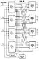
- Sequencer 13 i comprises a multiplexer 40 for multiplexing signals from the i th output terminals of packet switches 121 - 124 into a single data bit stream for coupling to a timeslot number detector 41 in which the timeslot number of each packet is removed from the packet and applied to a multiplexer 48, while packets destined to the same output port are supplied to a packet memory (dual-port RAM) in sequence.
- a write address generator 43 applies sequential write address data to memory 44 so that packets are stored into memory 44 in the order of arrival at the packet sequencer.
- the write address data is also applied to multiplexer 48 in which it is combined with a timeslot number to form a data set.
- Latches 491 - 49 n are connected in a series circuit to store and shift a data set from one latch to the next and from one latch to a corresponding one of compare-and-select circuits 501 ⁇ 50 n which are also connected in series between the output of multiplexer 48 and latch 49 n .
- a difference detector 45 is supplied with the reference timeslot number from time base 16 to detect the difference between it and the timeslot number contained in the output of latch 491.
- the output of difference detector 45 is applied to a comparator 46 in which it is compared with a threshold value which represents a maximum delay time allowable for each packet and corresponds to the maximum number of packets outstanding in the packet switches.
- Comparator 46 generates an output signal when the difference output from detector 45 is greater than the threshold value and enables a gate 47 for coupling the address component of a data set from latch 491 to RAM 44 as a read address pointer for reading a packet therefrom corresponding to the timeslot number of that data set.
- Compare-and-select circuit 501 compares the timeslot number of the output of multiplexer 48 with the timeslot number of a data set stored in latch 491 and transfers the data set from multiplexer 48 to the next compare-and-select circuit 502 if the timeslot number from multiplexer 48 is greater than the timeslot number from latch 491 and interchanges the compared data sets and transfers the data set from latch 491 to the next compare-and-select circuit if the timeslot number from multiplexer 48 is smaller than the other.
- each of the succeeding compare-and-select circuits 50 i compares the timeslot number of the output of the preceding compare-and-select circuit with the timeslot number of a data set stored in corresponding latch 49 i and transfers the data set from the preceding compare-and-select circuit to the next compare-and-select circuit if the timeslot number from the preceding circuit is greater than the timeslot number from the corresponding latch and interchanges the compared data sets and transfers the data set from the corresponding latch to the next compare-and-select circuit if the timeslot number from the preceding circuit is smaller than the other.
- compare-and-select circuit 501 in which the timeslot number "15" is compared with the timeslot number "10" of the data set stored in latch 491.
- Compare-and-select circuit 501 transfers the data set ("6"/"15") to the next circuit 502 for comparison with the timeslot number "20" stored in corresponding latch 492.
- Compare-and-select circuit 502 thus interchanges data sets with latch 492 and transfer data set("12"/"20") to compare-and-select circuit 503 (Fig. 4B) for making a comparison with the timeslot number "22" stored in corresponding latch 493.
- data sets in latch 493 and compare-and-select circuit 503 are interchanged and data set ("5"/"22") from latch 493 is transferred to the next compare-and-select circuit (Fig. 4C).
- data sets stored in latches 491 ⁇ 493 are arranged in the order of timeslot numbers with the timeslot number stored in latch 491 being always the smallest of all timeslot numbers stored in latches 49.
- the timeslot number stored in latch 491 is applied to the difference detector 45. If the difference between it and the reference timeslot number is greater than the threshold value, comparator 46 enables gate 47 to pass the address component of the data set stored in latch 491 to RAM 44 as a read address pointer for reading the given packet mentioned above. Simultaneously, data sets stored in all latches 49 are shifted to the left as shown in Fig. 4D.
- the output of difference detector 45 indicates the amount of time a packet has elapsed from the time at which a timeslot number is assigned to it by a packet distributer 11 i .
- each packet is read out of memory 44 following the detection of a maximum delay time within which an outstanding packet having a smaller timeslot number than any of the packets in the sequencer 13 i may possible exist in a packet switch 12.
- the packet read out of memory 44 is ensured that it is the earliest of all packets in a packet sequencer 13 i for a given instant of time.
- sequencer 13 i includes a multiplexer 60 in which the output signals from the i th output terminals of all packet switches 12 are multiplexed into a series of packets.
- the output of multiplexer 60 is connected to address filters 611 ⁇ 614 to which dual-port RAMs 621 - 624 are respectively connected.
- Each address filter 61 i examines each packet for the input-port address generated by the address generator 23 of a packet distributer 11 i (Fig. 2) and detects a match or mismatch with the own filter address.
- the address filter passes the matched packet to the associated memory 62. Therefore, packets coming from the same input port 10 i are passed through address filter 61 i and stored into packet memory 62 i .
- Memory controllers 63 i are associated respectively with address filters 61 i and packet memories 62 i to provide read/write control on associated packets for sequential delivery to a multiplexer 64 in which the packets having the same destination but coming from different input ports 11 are sequentially arranged and delivered to output port 14 i .
- Each memory controller 63 i comprises a timeslot number detector 65 coupled to the associated address filter 61 i to extract a timeslot number from each packet for coupling to a timeslot-to-address conversion table 66.
- the write address data from table 66 is applied to packet memory 62 i .
- a read control circuit 67 monitors the output of address filter 61 i to supply a read enable pulse to a read address generator 68 when the highest of timeslot numbers is reached to start sequential reading of packets from RAM 62 i . In this way, packets which might have arrived out of sequence are arranged into the right order.
- Sequencer 13 i includes first-in-first-out memories 701 ⁇ 704 for storing packets from the i th output terminals of packet switches 121 ⁇ 124, respectively.
- Timeslot number detectors 711 ⁇ 714 are respectively coupled to the end storage cell of the memories 701 ⁇ 704 for examining packets of earliest arrival to detect their timeslot numbers.
- the outputs of timeslot number detectors 711 ⁇ 714 are applied to a read control and minimum detection circuit 72 for detecting the smallest of the timeslot numbers supplied from timeslot number detectors 71 and applies a shift-out pulse to one of the FIFO memories corresponding to the smallest time slot number.
- a full empty detector 73 is connected to all FIFO memories 70 to disable the read control and minimum detection circuit 72 when at least one of the packet memories 70 is all empty to prevent an out-of-sequence situation which might occur if there is a packet outstanding in a packet switch 12 which is earlier than any of those in the FIFO memories 70.
- a third modification of the packet sequencer 13 i is illustrated as comprising timeslot number (TSN) detectors 801 - 804 connected respectively to the i th output terminals of all packet switches 12.
- TSN detectors 80 extract timeslot numbers from received packets and stores the timeslot numbers into TSN memories (FIFO) 821 - 824, respectively. With the timeslot numbers being removed, the packets from TSN detectors 801 - 804 are stored into FIFO memories 811 ⁇ 814, respectively, whose outputs are coupled together to output ports 14 i .
- a read control and sequential selection (RCSS) circuit 83 is connected to the output ends of TSN memories 82 to sequentially read the timeslot numbers of earliest arrivals and sequentially apply a select command signal to a shift pulse generator 8.
- the read timeslot numbers sequentially read out from memories 82 are supplied from RCSS circuit 83 to a comparator 85 for comparison with a timeslot number supplied from a local timeslot number generator 86.
- comparator 85 supplies an enable pulse to shift pulse generator 84 to allow it to apply the select command signal from RCSS circuit 83 to a packet memory 81 k to shift out the packet from that memory to output port 14 i .
- the same shift pulse is applied to the corresponding timeslot memory 82 k .
- comparator 85 causes timeslot number generator 86 to increment its value by one.
- a full empty detector 87 is provided for disabling the RCSS circuit 83 if at least one of the memories 81 is all empty to prevent the possible out-of-sequence situation as mentioned above.
- a fourth embodiment of the packet sequencer 13 i is shown in Fig. 8. Respective packets from the packet switches 12 are supplied to timeslot number detectors 901 ⁇ 904 on the one hand and stored into FIFO packet memories 911 - 914 on the other hand. To the output ends of FIFO memories 91 are respectively connected timeslot number detectors 92 whose outputs are, in turn, connected to a read control and sequential selection (RCSS) circuit 93 which sequentially read the outputs of timeslot detectors 92 for coupling to a comparator 94 in which it is compared with the output of a local timeslot number generator 95.
- RCSS read control and sequential selection
- the RCSS circuit 93 supplies a select command signal which is sequentially applied to a shift pulse generator 96 when enabled in response to the detection of a match by comparator 94 between the two timeslot numbers in a manner similar to the embodiment of Fig. 7, so that one of the packet memories 91 is shifted in response to a shift-out pulse supplied from generator 96.
- TSN generator 95 is incremented by one in response to the detection of a mismatch between the timeslot numbers by comparator 94.
- a full empty detector 98 is connected to all packet memories 91 to enable the TSN detectors 90 when at least one of the packet memories is empty, while disabling the RCSS circuit 93.
- the output of TSN generator 95 is further applied to a comparator 97 for comparison with the outputs of TSN detectors 90 when enabled by the full empty detector 98.
- TSN generator 95 is also incremented by one in response to an output signal from comparator 97 which is generated when the locally generated timeslot number is determined by the comparator as being smaller than any of the detected timeslot numbers.
- end-of-sequence detectors 991 ⁇ 994 To the outputs of packet memories 91 are respectively connected end-of-sequence detectors 991 ⁇ 994. Each of these end-of-sequence detectors 99 monitors successive output packets from the associated packet memory to detect the absence of a packet to follow. If the absence of a subsequent packet is detected, each end-of-sequence detector 99 causes the TSN generator 95 to increment its value by one.
- the packet memories 91 If one of the packet memories 91 is empty, a situation arises that a subsequent packet to fill that vacant memory will have a timeslot number greater than the current value of the locally generated timeslot number. If this is the case, the locally generated timeslot number is smaller than any of the detected timeslot numbers, and comparator 97 produces an output signal for incrementing TSN generator 95. On the other hand, when there is no subsequent output packet from one of the packet memories 91, the corresponding end-of-sequence detector 99 supplies an increment command signal to the TSN generator 95. By incrementing the TSN generator in this way, the total amount of time taken to process packets in the sequencers can be decreased.
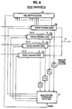
- Fig. 9 is a block diagram of a modified packet switching system in which each packet switch 12 produces a traffic load signal indicating the count of packets outstanding in the packet switch and transmits this signal to all packet distributers 11. The purpose of this modification is to evenly distribute packets over packet switches 12.
- each packet distributer includes a priority controller 100 which receives packet count signals from packet switches 121 ⁇ 124.
- each packet switch 12 is shown including a packet counter 110 having inputs coupled respectively to the FIFO memories 331 ⁇ 334. Packet counter 110 produces a signal indicating the total count of packets stored in the FIFO memories 33.
- the priority controller 100 uses the packet counts from all packet switches and controls the switch 24 for selecting the latches 26 so that those associated with the packet switches having a smaller number of outstanding packets are selected with higher priority than those associated with the packet switches in which a greater number of packets are outstanding More specifically, priority controller 100 determines whether the count of outstanding packets in one or more packet switches exceeds a predetermined value, and if so, it proceeds to select the packet switches other than the packet switch of which the packet count value is determined as exceeding the predetermined value.
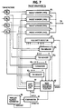
- each packet distributer 11 i is preferably provided with a destination address detector 120 coupled to the packet detector 20. The output of this detector is applied to a priority controller 121 to which traffic load signals are supplied from all packet switches. As shown in Fig. 13, each packet switch 12 includes a destination address detector 130 coupled to the FIFO memories 33 to detect the destination addresses of the packets stored therein. The packet counter 110 produces traffic load signals each indicating the packet count for each destination, so that the signal indicates the traffic condition the destination packet sequencer 13 as well as the intermediate packet switches.
- priority controller 121 uses the output of destination address detector 120 to analyze the traffic signals from packet switches 12 and makes a search through the packet switches 121 to 124 to determine one or more packet switches of which the packet count value of the same destination address exceeds a predetermined value. If this is the case, priority controller 121 selects the packet switches other than such modules with priority.
Abstract
Description
- The present invention relates generally to packet switching systems, and more specifically to a fast packet switching system for ISDN (Integrated Services Digital Network).
- Research effort has currently been focused on fast packet switching systems for transporting and switching all classes of information by segmenting signals into small packets and transporting them using simplified protocols. An architecture of such a fast packet switching system is described in a paper "A shared buffer memory switch for an ATM exchange", H. Kuwahara et al, (CH2655-9/89/0000-0118) 1989, IEEE. According to this technique, incoming packets are bit-sliced by a serial-to-parallel converters into packet segments for coupling to respective connection oriented sub-switching systems, and sequenced again by parallel-to-serial converters into the original packet at the output port. If the incoming packet has an L-bit length, it can be bit sliced to a maximum of L packet segments, allowing the sub-switching systems to operate at a speed 1/L of the speed of serial processing.
- The switching speed of the prior art packet switching systems is given by the relation N x V/K, where V is the line transmission speed, N the number of input ports, and K the number of packet segments into which each packet is bit-sliced. For a given switching speed, the line speed and the number of input ports can be increased by increasing the K value whose maximum value is equal to the bit length L. Typical values are N = 32, V = 4.8 Gbps, and L = K = 53 bytes for a switching speed of 362 Mbps. However, this value is still too high for implementing packet switching systems.
- It is therefore an object of the present invention to provide a packet switching system which is allowed to operate at a switching speed which is suitable for practical implementations.
- According to the present Invention, there is provided a packet switching system having a plurality of input ports and a plurality of output ports. The system comprises a plurality of packet distributers associated respectively with the input ports for receiving successive packets therefrom, each of the packet distributers attaching a timeslot number to each of the received packets, and uniformly distributing the packets to a plurality of output terminals thereof. A plurality of packet switches comprise the center stage of the system. These packet switches correspond in number to the output terminals of each of the packet distributers, and each of the packet switches has a plurality of input terminals corresponding in number to the packet distributers and a plurality of output terminals corresponding in number to the output ports. The input terminals of each packet switch are coupled to respective output terminals of the packet distributers for switching a packet from one of the input terminals thereof to one of the output terminals thereof in accordance with a destination address contained in the packet. A plurality of packet sequencers are associated respectively with the output ports. Each of the packet sequencers has a plurality of input terminals coupled to respective output terminals of the packet switches for examining the timeslot numbers attached to packets from the input terminals thereof and delivering the packets to the associated output port in accordance with the examined timeslot numbers.
- For uniform distribution of packets to the center stage, each of the packet switches generates a traffic-related signal indicating the amount of packets outstanding in the packet switch. Each packet distributer receives the traffic-related signal from each packet switch and gives priority to the output terminals of the packet distributer according to the amounts of packets outstanding in the respective packet switches. In this way, packets from the associated input port are distributed with priority to those of the packet switches containing a smaller amount of outstanding packets.
- Although self-routing switches are of benefit for certain applications, bit-slicing technique can be used for higher speed switching application. If bit-slicing technique is used for the center switching stage, the switching speed of the system can be decreased to N x V/P x L, where P is the number of switches of the center stage.
- The present invention will be described in further detail with reference to the accompanying drawings, in which:
- Fig. 1 is a block diagram of a packet switching system of the present invention;
- Fig. 2 is a block diagram showing details of each packet distributer of Fig. 1;
- Fig. 3 is a block diagram showing details of each packet switch;
- Fig. 4 is a block diagram showing one embodiment of a packet sequencer, Figs. 4A to 4D showing data sets moving through packet reordering circuit of the sequencer;
- Fig. 5 is a block diagram showing a first modification of the packet sequencer;
- Fig. 6 is a block diagram of a second modification of the packet sequencer;
- Fig. 7 is a block diagram of a third modification of the packet sequencer;
- Fig. 8 is a block diagram of a fourth modification of the packet sequencer;
- Fig. 9 is a block diagram of the packet switching system according to a second embodiment of this invention;
- Fig. 10 shows details of a packet distributer of Fig. 9;
- Fig. 11 shows details of a packet switch of Fig. 9;
- Fig. 12 shows details of a modified form of the packet distributer of Fig. 9; and
- Fig. 13 shows details of a modified form of the packet switch of Fig. 9 associated with the modified packet distributer of Fig. 12.
- Referring now to Fig. 1, there is shown a packet switching system according to one embodiment of the present invention. For purposes of illustration, the switching system has four
input ports 10₁ through 10₄ for receiving packets of a predetermined bit length from user stations at a line clock rate specified by the system and switching the received packets to one of fouroutput ports 14₁ through 14₄. Each packet contains a label indicating a destination user station. The system comprises a plurality ofpacket distributers 11₁ ∼ 11₄ corresponding respectively to theinput ports 10₁ ∼ 10₄, a plurality of 4 x 4 self-routing packet switches 12₁ - 12₄ corresponding in number to the packet distributers, and a like plurality of packet sequencers 13₁ - 13₄ corresponding respectively to theoutput ports 14₁ ∼ 14₄. Eachpacket distributer 11i has four output terminals coupled respectively to the ith input terminals of allpacket switches 12. The output terminals of eachpacket switch 12i are coupled respectively to the ith input terminals of allpacket sequences 13. - On receiving a packet, each
packet distributer 11i extracts the label from the packet and uses it to reference a routing table 15 to attach an outgoing address identifying one of the output ports 14. The distributer proceeds to attach a timeslot number to the packet, selects one of thepacket switches 12 and applies the packet to the selected packet switch so that packets received successively from a given user are distributed uniformly to the packet switches. To assign a timeslot number, a series of reference timeslot numbers is cyclically generated by asystem time base 16 and supplied to allpacket distributers 11. In each self-routing packet switch 12, each packet is examined for its destination and routed to one of thepacket sequencers 13 according to the outgoing identifier contained in the label. Because of the paral!el switching of successive packets bypacket switches 12₁ ∼ 12₄, each packet switch is given an interval for switching which is four times longer than would otherwise be allowed if the burden is placed on a single packet switch. - Packets destined to a given output port may arrive at the packet sequencer associated with that port at different times. To secure packet sequence integrity, each packet sequencer extracts the time stamp from each packet and uses it to rearrange successive packets in the original sequence.
- Details of the system components will now be described. In Fig. 2, each
packet distributer 11i of Fig. 1 comprises apacket detector 20 coupled to the associatedinput port 10i for extracting a label from each incoming packet and applies it to the routing table 15 to rewrite its label with an outgoing address obtained from the routing table and applies its output to amultiplexer 22. Simultaneously, it informs the arrival of a packet to a timeslot number (TSN)assignment circuit 21 to which the reference timeslot number is supplied from thetime base 16. In a practical embodiment, each of the packet switches may hold a sequence of a maximum of, say, 100 outstanding packets. In order to allow identification of packets arriving at a given packet sequencer, timeslot numbers #1 through #100 are assigned respectively to one hundred packets of each successive sequence and the same numbers are cyclically used. TheTSN assignment circuit 21 assigns a timeslot number to each packet in response to an output signal frompacket detector 20 and applies the assigned number tomultiplexer 22 so that the packet is multiplexed with the assigned timeslot number which is unique to the sequence of 100 packets to which it belongs. - An input-
port address generator 23 is also connected tomultiplexer 22 to append an identifier identifying theinput port 10i. This identifier will be used by the packet sequencers constructed according to one embodiment of this invention. - The output of
multiplexer 22 is applied to aswitch 24 which applies packets frommultiplexer 22 to latches 26 in accordance with a switching signal supplied from acontroller 25. The outputs oflatches 26₁ ∼ 26₄ ofpacket distributer 11i are respectively connected to the ith input terminals ofpacket switches 12₁ ∼ 12₄.Controller 25 sequentially selects latches 26 so that successive packets are sequentially distributed to all latches 26. At periodic clock intervals, the packets stored in latches 26 are simultaneously forwarded to thecorresponding packet switches 12. - As shown in Fig. 3, each self-
routing packet switch 12i comprises amultiplexer 30 for multiplexing signals from the ith outputs of allpacket distributers 11 and forwarding the multiplexed signal onto acommon bus 31 to which are connected address filters 32₁ - 32₄ having filter addresses identifying respectively theoutput ports 14₁ ∼ 14₄. First-in-first-outmemories 33₁∼33₄ are connected respectively to the outputs of address filters 32₁ - 32₄, the output ofFIFO memories 33₁∼33₄ of eachpacket switch 12i being connected to the ith inputs of packet sequencers 13₁ - 13₄, respectively. Each address filter 32 examines the outgoing address contained in each of packets arriving from thedifferent packet distributers 11 and detects a match or mismatch with the address of the filter 32. On detecting a match, each address filter 32i allows a packet to be passed therethrough to corresponding FIFO memory 33i. The outputs ofFIFO memories packet switch 12i are connected to the ith input terminals ofpacket sequencers - Fig. 4 shows one embodiment of
packet sequencer 13i.Sequencer 13i comprises amultiplexer 40 for multiplexing signals from the ith output terminals of packet switches 12₁ - 12₄ into a single data bit stream for coupling to atimeslot number detector 41 in which the timeslot number of each packet is removed from the packet and applied to amultiplexer 48, while packets destined to the same output port are supplied to a packet memory (dual-port RAM) in sequence. Awrite address generator 43 applies sequential write address data tomemory 44 so that packets are stored intomemory 44 in the order of arrival at the packet sequencer. The write address data is also applied tomultiplexer 48 in which it is combined with a timeslot number to form a data set. Latches 49₁ - 49n are connected in a series circuit to store and shift a data set from one latch to the next and from one latch to a corresponding one of compare-and-select circuits 50₁ ∼ 50n which are also connected in series between the output ofmultiplexer 48 and latch 49n. Adifference detector 45 is supplied with the reference timeslot number fromtime base 16 to detect the difference between it and the timeslot number contained in the output oflatch 49₁. The output ofdifference detector 45 is applied to acomparator 46 in which it is compared with a threshold value which represents a maximum delay time allowable for each packet and corresponds to the maximum number of packets outstanding in the packet switches.Comparator 46 generates an output signal when the difference output fromdetector 45 is greater than the threshold value and enables agate 47 for coupling the address component of a data set fromlatch 49₁ to RAM 44 as a read address pointer for reading a packet therefrom corresponding to the timeslot number of that data set. Compare-and-select circuit 50₁ compares the timeslot number of the output ofmultiplexer 48 with the timeslot number of a data set stored inlatch 49₁ and transfers the data set frommultiplexer 48 to the next compare-and-select circuit 50₂ if the timeslot number frommultiplexer 48 is greater than the timeslot number fromlatch 49₁ and interchanges the compared data sets and transfers the data set fromlatch 49₁ to the next compare-and-select circuit if the timeslot number frommultiplexer 48 is smaller than the other. Likewise, each of the succeeding compare-and-select circuits 50i compares the timeslot number of the output of the preceding compare-and-select circuit with the timeslot number of a data set stored in corresponding latch 49i and transfers the data set from the preceding compare-and-select circuit to the next compare-and-select circuit if the timeslot number from the preceding circuit is greater than the timeslot number from the corresponding latch and interchanges the compared data sets and transfers the data set from the corresponding latch to the next compare-and-select circuit if the timeslot number from the preceding circuit is smaller than the other. - The operation of this packet sequencer will best be understood with reference to Figs. 4A ∼ 4D. For purposes of simplicity, it is assumed that only three sets of compare-and-select circuits and corresponding latches are provided. Assume that a given packet has a timeslot number "15" and is stored in
RAM 44 in a location identified by write address data "6". This timeslot number is combined bymultiplexer 48 with the timeslot number "15" supplied fromwrite address generator 43 to produce a data set ("6"/"15"). Up to this point, data sets ("8"/"10"), ("12"/"20") and ("5"/"22") are assumed to have been stored respectively inlatches multiplexer 48 is applied to compare-and-select circuit 50₁ in which the timeslot number "15" is compared with the timeslot number "10" of the data set stored inlatch 49₁. Compare-and-select circuit 50₁ transfers the data set ("6"/"15") to thenext circuit 50₂ for comparison with the timeslot number "20" stored incorresponding latch 49₂. Compare-and-select circuit 50₂ thus interchanges data sets withlatch 49₂ and transfer data set("12"/"20") to compare-and-select circuit 50₃ (Fig. 4B) for making a comparison with the timeslot number "22" stored incorresponding latch 49₃. Thus, data sets inlatch 49₃ and compare-and-select circuit 50₃ are interchanged and data set ("5"/"22") fromlatch 49₃ is transferred to the next compare-and-select circuit (Fig. 4C). - In this way, data sets stored in
latches 49₁ ∼ 49₃ are arranged in the order of timeslot numbers with the timeslot number stored inlatch 49₁ being always the smallest of all timeslot numbers stored in latches 49. At the end of this process, the timeslot number stored inlatch 49₁ is applied to thedifference detector 45. If the difference between it and the reference timeslot number is greater than the threshold value,comparator 46 enablesgate 47 to pass the address component of the data set stored inlatch 49₁ to RAM 44 as a read address pointer for reading the given packet mentioned above. Simultaneously, data sets stored in all latches 49 are shifted to the left as shown in Fig. 4D. - Since the reference timeslot number represents the real time, the output of
difference detector 45 indicates the amount of time a packet has elapsed from the time at which a timeslot number is assigned to it by apacket distributer 11i. Thus, each packet is read out ofmemory 44 following the detection of a maximum delay time within which an outstanding packet having a smaller timeslot number than any of the packets in thesequencer 13i may possible exist in apacket switch 12. Thus, the packet read out ofmemory 44 is ensured that it is the earliest of all packets in apacket sequencer 13i for a given instant of time. - The packet sequencers are modified in several forms as shown in Figs. 5 to 8. In Fig. 5,
sequencer 13i includes amultiplexer 60 in which the output signals from the ith output terminals of all packet switches 12 are multiplexed into a series of packets. The output ofmultiplexer 60 is connected to addressfilters 61₁ ∼ 61₄ to which dual-port RAMs 62₁ - 62₄ are respectively connected. The address of each filter 61i (where i = 1, 2, 3, 4) corresponds to the address of theinput port 10i. Each address filter 61i examines each packet for the input-port address generated by theaddress generator 23 of a packet distributer 11i (Fig. 2) and detects a match or mismatch with the own filter address. If a match is detected, the address filter passes the matched packet to the associated memory 62. Therefore, packets coming from thesame input port 10i are passed through address filter 61i and stored into packet memory 62i. Memory controllers 63i are associated respectively with address filters 61i and packet memories 62i to provide read/write control on associated packets for sequential delivery to amultiplexer 64 in which the packets having the same destination but coming fromdifferent input ports 11 are sequentially arranged and delivered to output port 14i. - Each memory controller 63i comprises a
timeslot number detector 65 coupled to the associated address filter 61i to extract a timeslot number from each packet for coupling to a timeslot-to-address conversion table 66. There is a map in the conversion table 66 uniquely specifying relationships between all timeslot numbers and corresponding storage locations of memory 62i. It is seen therefore that conversion table 66 can produce a write address corresponding to each timeslot number, and hence all packets stored in RAM 62i can be sequentially readable. The write address data from table 66 is applied to packet memory 62i. Aread control circuit 67 monitors the output of address filter 61i to supply a read enable pulse to aread address generator 68 when the highest of timeslot numbers is reached to start sequential reading of packets from RAM 62i. In this way, packets which might have arrived out of sequence are arranged into the right order. - A simplified form of
sequencer 13i is shown in Fig. 6.Sequencer 13i includes first-in-first-out memories 70₁ ∼ 70₄ for storing packets from the ith output terminals ofpacket switches 12₁ ∼ 12₄, respectively.Timeslot number detectors 71₁ ∼ 71₄ are respectively coupled to the end storage cell of the memories 70₁ ∼ 70₄ for examining packets of earliest arrival to detect their timeslot numbers. The outputs oftimeslot number detectors 71₁ ∼ 71₄ are applied to a read control andminimum detection circuit 72 for detecting the smallest of the timeslot numbers supplied from timeslot number detectors 71 and applies a shift-out pulse to one of the FIFO memories corresponding to the smallest time slot number. In this way, a packet arriving earliest of those stored in the output ends of FIFO memories 70₁ ∼ 70₄ is shifted out of a FIFO memory 70k to output port 14i. The same process is repeated to deliver a packet of second arrival from the output end of another FIFO memory. A fullempty detector 73 is connected to all FIFO memories 70 to disable the read control andminimum detection circuit 72 when at least one of the packet memories 70 is all empty to prevent an out-of-sequence situation which might occur if there is a packet outstanding in apacket switch 12 which is earlier than any of those in the FIFO memories 70. - In Fig. 7, a third modification of the
packet sequencer 13i is illustrated as comprising timeslot number (TSN) detectors 80₁ - 80₄ connected respectively to the ith output terminals of all packet switches 12. TSN detectors 80 extract timeslot numbers from received packets and stores the timeslot numbers into TSN memories (FIFO) 82₁ - 82₄, respectively. With the timeslot numbers being removed, the packets from TSN detectors 80₁ - 80₄ are stored intoFIFO memories 81₁ ∼ 81₄, respectively, whose outputs are coupled together to output ports 14i. A read control and sequential selection (RCSS)circuit 83 is connected to the output ends of TSN memories 82 to sequentially read the timeslot numbers of earliest arrivals and sequentially apply a select command signal to ashift pulse generator 8. The read timeslot numbers sequentially read out from memories 82 are supplied fromRCSS circuit 83 to a comparator 85 for comparison with a timeslot number supplied from a localtimeslot number generator 86. When the timeslot numbers are equal, comparator 85 supplies an enable pulse to shiftpulse generator 84 to allow it to apply the select command signal fromRCSS circuit 83 to a packet memory 81k to shift out the packet from that memory to output port 14i. The same shift pulse is applied to the corresponding timeslot memory 82k. If they mismatch, comparator 85 causestimeslot number generator 86 to increment its value by one. A fullempty detector 87 is provided for disabling theRCSS circuit 83 if at least one of the memories 81 is all empty to prevent the possible out-of-sequence situation as mentioned above. - A fourth embodiment of the
packet sequencer 13i is shown in Fig. 8. Respective packets from the packet switches 12 are supplied totimeslot number detectors 90₁ ∼ 90₄ on the one hand and stored into FIFO packet memories 91₁ - 91₄ on the other hand. To the output ends of FIFO memories 91 are respectively connectedtimeslot number detectors 92 whose outputs are, in turn, connected to a read control and sequential selection (RCSS)circuit 93 which sequentially read the outputs oftimeslot detectors 92 for coupling to acomparator 94 in which it is compared with the output of a localtimeslot number generator 95. TheRCSS circuit 93 supplies a select command signal which is sequentially applied to ashift pulse generator 96 when enabled in response to the detection of a match bycomparator 94 between the two timeslot numbers in a manner similar to the embodiment of Fig. 7, so that one of the packet memories 91 is shifted in response to a shift-out pulse supplied fromgenerator 96.TSN generator 95 is incremented by one in response to the detection of a mismatch between the timeslot numbers bycomparator 94. - A full
empty detector 98 is connected to all packet memories 91 to enable the TSN detectors 90 when at least one of the packet memories is empty, while disabling theRCSS circuit 93. The output ofTSN generator 95 is further applied to acomparator 97 for comparison with the outputs of TSN detectors 90 when enabled by the fullempty detector 98.TSN generator 95 is also incremented by one in response to an output signal fromcomparator 97 which is generated when the locally generated timeslot number is determined by the comparator as being smaller than any of the detected timeslot numbers. - To the outputs of packet memories 91 are respectively connected end-of-
sequence detectors 99₁ ∼ 99₄. Each of these end-of-sequence detectors 99 monitors successive output packets from the associated packet memory to detect the absence of a packet to follow. If the absence of a subsequent packet is detected, each end-of-sequence detector 99 causes theTSN generator 95 to increment its value by one. - If one of the packet memories 91 is empty, a situation arises that a subsequent packet to fill that vacant memory will have a timeslot number greater than the current value of the locally generated timeslot number. If this is the case, the locally generated timeslot number is smaller than any of the detected timeslot numbers, and
comparator 97 produces an output signal for incrementingTSN generator 95. On the other hand, when there is no subsequent output packet from one of the packet memories 91, the corresponding end-of-sequence detector 99 supplies an increment command signal to theTSN generator 95. By incrementing the TSN generator in this way, the total amount of time taken to process packets in the sequencers can be decreased. - Fig. 9 is a block diagram of a modified packet switching system in which each
packet switch 12 produces a traffic load signal indicating the count of packets outstanding in the packet switch and transmits this signal to allpacket distributers 11. The purpose of this modification is to evenly distribute packets over packet switches 12. - As shown in Fig. 10, each packet distributer includes a
priority controller 100 which receives packet count signals frompacket switches 12₁ ∼ 12₄. In Fig. 11, eachpacket switch 12 is shown including apacket counter 110 having inputs coupled respectively to theFIFO memories 33₁ ∼ 33₄.Packet counter 110 produces a signal indicating the total count of packets stored in the FIFO memories 33. - Returning to Fig. 10, the
priority controller 100 uses the packet counts from all packet switches and controls theswitch 24 for selecting the latches 26 so that those associated with the packet switches having a smaller number of outstanding packets are selected with higher priority than those associated with the packet switches in which a greater number of packets are outstanding More specifically,priority controller 100 determines whether the count of outstanding packets in one or more packet switches exceeds a predetermined value, and if so, it proceeds to select the packet switches other than the packet switch of which the packet count value is determined as exceeding the predetermined value. - In Fig. 12, each
packet distributer 11i is preferably provided with adestination address detector 120 coupled to thepacket detector 20. The output of this detector is applied to apriority controller 121 to which traffic load signals are supplied from all packet switches. As shown in Fig. 13, eachpacket switch 12 includes adestination address detector 130 coupled to the FIFO memories 33 to detect the destination addresses of the packets stored therein. Thepacket counter 110 produces traffic load signals each indicating the packet count for each destination, so that the signal indicates the traffic condition thedestination packet sequencer 13 as well as the intermediate packet switches. In eachpacket distributer 11,priority controller 121 uses the output ofdestination address detector 120 to analyze the traffic signals frompacket switches 12 and makes a search through the packet switches 12₁ to 12₄ to determine one or more packet switches of which the packet count value of the same destination address exceeds a predetermined value. If this is the case,priority controller 121 selects the packet switches other than such modules with priority. - The foregoing description shows only preferred embodiments of the present invention. Various modifications are apparent to those skilled in the art without departing from the scope of the present invention which is only limited by the appended claims. Therefore, the embodiments shown and described are only illustrative, not restrictive.
Claims (14)
- A packet switching system having a plurality of input ports and a plurality of output ports, comprising:
a plurality of packet distributers associated respectively with the input ports for receiving successive packets therefrom, each of said packet distributers attaching a timeslot number to each of the received packets, and uniformly distributing the packets to a plurality of output terminals thereof;
a plurality of packet switches corresponding in number to the output terminals of each of the packet distributers, each of the packet switches having a plurality of input terminals corresponding in numbers to the packet distributers and a plurality of output terminals corresponding in number to said output ports, the input terminals of each packet switch being coupled to respective output terminals of said packet distributers for switching a packet from one of the input terminals thereof to one of the output terminals thereof in accordance with a destination address contained in the packet; and
a plurality of packet sequencers associated respectively with said output ports, each of the packet sequencers having a plurality of input terminals coupled to respective output terminals of the packet switches for examining the timeslot numbers attached to packets from the input terminals thereof and delivering the packets to the associated output port in accordance with the examined timeslot numbers. - A packet switching system as claimed in claim 1, wherein each of said packet switches comprises means for generating a traffic-related signal indicating the amount of packets outstanding in the packet switch, and wherein each of the packet distributers comprises means for receiving said traffic-related signal from each of the packet switches and giving priority of packet distribution to the output terminals of the packet distributer according to the amounts of packets outstanding in the respective packet switches so that packets from the associated input port are distributed with priority to those of the packet switches having a smaller amount of outstanding packets.
- A packet switching system as claimed in claim 1 or 2, wherein each of said packet switches comprises:
means for detecting destination addresses from packets respectively destined to said output ports; and
means for generating a traffic-related signal indicating the respective amounts of said packets having said detected destination addresses, and wherein each of the packet distributers comprises:
means for detecting the destination addresses of incoming packets from the associated input port; and
means for receiving said traffic-related signal from each of the packet switches and giving priority of packet distribution to the output terminals of the packet distributer according to the amounts of packets indicated by the traffic-related signal and according to the detected destination addresses of said incoming packets so that the incoming packets are distributed with priority to those of the packet switches having a smaller amount of packets containing the same destination address as said incoming packets. - A packet switching system as claimed in claim 1, 2, or 3, wherein each of said packet sequencers comprises:
multiplexer means for multiplexing packets from the input terminals thereof;
timeslot detector means for detecting the timeslot number of said multiplexed packets;
address generator means for generating address signals corresponding to said multiplexed packets, respectively;
memory means responsive to said address signals for storing said multiplexed packets in locations respectively identified by said address signals;
combiner means for combining the address signals and the detected timeslot numbers to produce data sets;
packet arranging means for arranging said data sets according to the timeslot numbers contained therein; and
gate means for applying the address signals contained in the arranged data sets to said memory means for reading packets stored therein. - A packet switching system as claimed in claim 4, wherein said packet arranging means comprises:
a plurality of latches series-connected in a first circuit; and
a like plurality of compare-and-select circuits series-connected in a second circuit, said compare-and-select circuits being connected to corresponding ones of said latches and to said combiner means for receiving the data set from the combiner means, each of the compare-and-select circuits comparing the timeslot number of each data set in said first circuit with the timeslot number of each data set in said second circuit and interchanging the data sets between said first and second circuits and applying the data set from the first circuit to a subsequent compare-and-select circuit when the timeslot number of the data set in said second circuit is smaller than the timeslot number of the data set in said first circuit, so that data sets stored in said latches are arranged according to the timeslot numbers thereof. - A packet switching system as claimed in claim 4 or 5, wherein said gate means comprises:
means for detecting a difference between the timeslot number of each data set stored in one of said latches and a reference timeslot number; and
means for comparing said difference with a threshold value and applying the address signal contained in the data set stored in said one of said latches to said memory means when said difference exceeds said threshold value. - A packet switching system as claimed in claim 6, wherein said threshold value represents a maximum number of packets outstanding in each of said packet switches.
- A packet switching system as claimed in any one of claims 1 to 7, wherein each of said packet distributers comprises means for attaching an input-port address identifying the associated input port, and wherein each of said packet sequencers comprises:
first multiplexer means for multiplexing packets from the input terminals of the packet sequencer;
a plurality of address filter means corresponding respectively to said input ports, each of the address filter means being coupled to said first multiplexer means and having the input-port address of the corresponding input port for detecting packets from the output of the multiplexer means having the same input-port address as the address filter means;
a plurality of memory means coupled respectively to said address filter means;
a plurality of memory control means associated respectively with said address filter means and with said memory means, each of the memory control means comprising means for detecting timeslot numbers from the packets detected by the associated address filter means, means for generating write address signals corresponding to said detected timeslot numbers for storing the packets detected by the associated address filter means into said associated memory means according to said write address signals, and means for sequentially generating read address signals for reading packets from the associated memory means according to said read address signals; and
second multiplexer means for multiplexing packets read out of said plural memory means. - A packet switching system as claimed in any one of claims 1 to 8, wherein each of said packet sequencers comprises:
a plurality of first-in-first-out memory means having input ends connected respectively to the input terminals of the packet sequencer and having output ends coupled together to the associated output port;
a plurality of timeslot number detectors connected respectively to the output ends of said first-in-first-out memory means; and
control means for detecting a minimum value of said detected timeslot numbers and shifting one of said first-in-first-out memories corresponding to the timeslot number of the detected minimum value. - A packet switching system as claimed in claim 9, wherein each of said packet sequencers further comprises means for detecting when at least one of said first-in-first-out memories is empty and disabling said control means.
- A packet switching system as claimed in any one of claims 1 to 10, wherein each of said packet sequencers comprises:
a plurality of timeslot number detectors coupled respectively to the input terminals of the packet sequencer for extracting timeslot numbers from packets arriving at said input terminals;
a first plurality of first-in-first-out memory means having input ends connected respectively to said timeslot number detectors for storing the packets from the timeslot number detectors and having output ends coupled together to the associated output port;
a second plurality of first-in-first-out memory means having input ends connected respectively to said timeslot number detectors for storing the timeslot numbers detected respectively by the timeslot number detectors;
timeslot number generator means for sequentially generating a local timeslot number; and
control means connected to the output ends of the first plurality of first-in-first-out memory means for sequentially reading the timeslot numbers stored in said output ends, comparing said local timeslot number and each of the timeslot numbers read out of said memory means to detect a match or mismatch therebetween, and shifting one of said first plurality of first-in-first-out memory means and one of said second plurality of first-in-first-out memory means when there is a match between said timeslot numbers and incrementing said timeslot number generator means when there is a mismatch between said timeslot numbers. - A packet switching system as claimed in claim 11, wherein wherein each of said packet sequencers further comprises means for detecting when at least one of said first plurality of first-in-first-out memories is empty and disabling said control means.
- A packet switching system as claimed in any one of claims 1 to 12, wherein each of said packet sequencers comprises:
a plurality of first-in-first-out memory means having input ends connected respectively to the input terminals of the packet sequencer and having output ends;
a first plurality of timeslot number detectors connected respectively to the output ends of said first-in-first-out memory means for detecting timeslot numbers from packets stored in said output ends;
timeslot number generator means for sequentially generating a local timeslot number;
control means connected to the first plurality of timeslot number detectors for sequentially reading the timeslot numbers detected by the first plurality of timeslot number detectors, comparing said local timeslot number and each of the timeslot numbers detected by the first plurality of timeslot number detectors to detect a match or mismatch therebetween, and shifting one of said first-in-first-out memory means when there is a match between said timeslot numbers and incrementing said timeslot number generator means when there is a mismatch between said timeslot numbers;
a second plurality of timeslot number detectors for detecting, when enabled, timeslot numbers from packets arriving at the input terminals of the packet sequencer;
means for detecting when at least one of said first-in-first-out memories is empty, disabling said control means and enabling said second plurality of timeslot number detectors to allow detection of said timeslot numbers;
means for detecting when each of the timeslot numbers detected by the second plurality of timeslot number detectors is greater than the local timeslot number and incrementing said timeslot number generator means; and
a plurality of end-of-sequence detector means connected respectively to the output ends of said first-in-first-out memory means for detecting when there is no packet to follow and incrementing said timeslot generator means. - A packet switching system as claimed in any one of claims 1 to 13, wherein each of said packet switches is a self-routing switch.
Applications Claiming Priority (6)
| Application Number | Priority Date | Filing Date | Title |
|---|---|---|---|
| JP52991 | 1991-01-08 | ||
| JP529/91 | 1991-01-08 | ||
| JP5797191A JP3163638B2 (en) | 1991-02-27 | 1991-02-27 | Packet switching method |
| JP57971/91 | 1991-02-27 | ||
| JP7282291A JP3163640B2 (en) | 1991-01-08 | 1991-04-05 | Packet switching method |
| JP72822/91 | 1991-04-05 |
Publications (3)
| Publication Number | Publication Date |
|---|---|
| EP0497097A2 true EP0497097A2 (en) | 1992-08-05 |
| EP0497097A3 EP0497097A3 (en) | 1992-09-09 |
| EP0497097B1 EP0497097B1 (en) | 1996-11-06 |
Family
ID=27274498
Family Applications (1)
| Application Number | Title | Priority Date | Filing Date |
|---|---|---|---|
| EP92100201A Expired - Lifetime EP0497097B1 (en) | 1991-01-08 | 1992-01-08 | Switching system with time-stamped packet distribution input stage and packet sequencing output stage |
Country Status (4)
| Country | Link |
|---|---|
| US (1) | US5253251A (en) |
| EP (1) | EP0497097B1 (en) |
| CA (1) | CA2059027C (en) |
| DE (1) | DE69214968T2 (en) |
Cited By (5)
| Publication number | Priority date | Publication date | Assignee | Title |
|---|---|---|---|---|
| EP0553798A2 (en) * | 1992-01-27 | 1993-08-04 | Nec Corporation | Low delay ATM switching system using stamped idle cells |
| WO1999007181A2 (en) * | 1997-07-14 | 1999-02-11 | Nokia Networks Oy | Switching fabric arrangement with time stamp function |
| EP1017248A1 (en) * | 1998-12-31 | 2000-07-05 | Alcatel | Method of resequencing data blocks in an asynchronous switching system |
| WO2002015489A2 (en) * | 2000-08-15 | 2002-02-21 | Conexant Systems, Inc. | Switches and routers, with parallel domains operating at a reduced speed |
| WO2004079961A2 (en) * | 2003-03-03 | 2004-09-16 | Xyratex Technology Limited | Apparatus and method for switching data packets |
Families Citing this family (98)
| Publication number | Priority date | Publication date | Assignee | Title |
|---|---|---|---|---|
| US5260935A (en) * | 1991-03-01 | 1993-11-09 | Washington University | Data packet resequencer for a high speed data switch |
| US5617547A (en) * | 1991-03-29 | 1997-04-01 | International Business Machines Corporation | Switch network extension of bus architecture |
| GB2258366B (en) * | 1991-08-02 | 1995-03-29 | Plessey Telecomm | An ATM switching arrangement |
| US5383181A (en) * | 1991-10-31 | 1995-01-17 | Nec Corporation | Packet switching system capable of reducing a delay time for each packet |
| JPH0646080A (en) * | 1992-07-22 | 1994-02-18 | Toshiba Corp | Delay aluctuation absorption control system |
| EP0602281B1 (en) * | 1992-11-30 | 2001-12-19 | Alcatel | Resequencing means for a cell switching system node |
| SE515419C2 (en) * | 1993-06-15 | 2001-07-30 | Ericsson Telefon Ab L M | Method and apparatus for travel sequencing |
| EP0639909A1 (en) * | 1993-08-17 | 1995-02-22 | ALCATEL BELL Naamloze Vennootschap | Resequencing system |
| US5444709A (en) * | 1993-09-30 | 1995-08-22 | Apple Computer, Inc. | Protocol for transporting real time data |
| US5481536A (en) * | 1993-10-29 | 1996-01-02 | Siemens Aktiengesellschaft | Method for restoring a prescribed sequence for unordered cell streams in ATM switching technology |
| US5602992A (en) * | 1993-11-29 | 1997-02-11 | Intel Corporation | System for synchronizing data stream transferred from server to client by initializing clock when first packet is received and comparing packet time information with clock |
| US5467349A (en) * | 1993-12-21 | 1995-11-14 | Trw Inc. | Address handler for an asynchronous transfer mode switch |
| US5412646A (en) * | 1994-05-13 | 1995-05-02 | At&T Corp. | Asynchronous transfer mode switch architecture |
| US5854898A (en) | 1995-02-24 | 1998-12-29 | Apple Computer, Inc. | System for automatically adding additional data stream to existing media connection between two end points upon exchange of notifying and confirmation messages therebetween |
| JPH0936912A (en) * | 1995-07-14 | 1997-02-07 | Fujitsu Ltd | Buffer control system |
| US6097718A (en) * | 1996-01-02 | 2000-08-01 | Cisco Technology, Inc. | Snapshot routing with route aging |
| US6147996A (en) * | 1995-08-04 | 2000-11-14 | Cisco Technology, Inc. | Pipelined multiple issue packet switch |
| US6917966B1 (en) | 1995-09-29 | 2005-07-12 | Cisco Technology, Inc. | Enhanced network services using a subnetwork of communicating processors |
| US7246148B1 (en) | 1995-09-29 | 2007-07-17 | Cisco Technology, Inc. | Enhanced network services using a subnetwork of communicating processors |
| US6182224B1 (en) | 1995-09-29 | 2001-01-30 | Cisco Systems, Inc. | Enhanced network services using a subnetwork of communicating processors |
| US6091725A (en) | 1995-12-29 | 2000-07-18 | Cisco Systems, Inc. | Method for traffic management, traffic prioritization, access control, and packet forwarding in a datagram computer network |
| US6035105A (en) | 1996-01-02 | 2000-03-07 | Cisco Technology, Inc. | Multiple VLAN architecture system |
| US6308148B1 (en) | 1996-05-28 | 2001-10-23 | Cisco Technology, Inc. | Network flow data export |
| US6243667B1 (en) | 1996-05-28 | 2001-06-05 | Cisco Systems, Inc. | Network flow switching and flow data export |
| US6434120B1 (en) | 1998-08-25 | 2002-08-13 | Cisco Technology, Inc. | Autosensing LMI protocols in frame relay networks |
| US6304546B1 (en) | 1996-12-19 | 2001-10-16 | Cisco Technology, Inc. | End-to-end bidirectional keep-alive using virtual circuits |
| US6122272A (en) * | 1997-05-23 | 2000-09-19 | Cisco Technology, Inc. | Call size feedback on PNNI operation |
| US6356530B1 (en) | 1997-05-23 | 2002-03-12 | Cisco Technology, Inc. | Next hop selection in ATM networks |
| US6862284B1 (en) | 1997-06-17 | 2005-03-01 | Cisco Technology, Inc. | Format for automatic generation of unique ATM addresses used for PNNI |
| US6078590A (en) * | 1997-07-14 | 2000-06-20 | Cisco Technology, Inc. | Hierarchical routing knowledge for multicast packet routing |
| US6330599B1 (en) | 1997-08-05 | 2001-12-11 | Cisco Technology, Inc. | Virtual interfaces with dynamic binding |
| US6512766B2 (en) | 1997-08-22 | 2003-01-28 | Cisco Systems, Inc. | Enhanced internet packet routing lookup |
| US6212183B1 (en) | 1997-08-22 | 2001-04-03 | Cisco Technology, Inc. | Multiple parallel packet routing lookup |
| US6157641A (en) * | 1997-08-22 | 2000-12-05 | Cisco Technology, Inc. | Multiprotocol packet recognition and switching |
| US6147991A (en) * | 1997-09-05 | 2000-11-14 | Video Network Communications, Inc. | Scalable high speed packet switch using packet diversion through dedicated channels |
| US6343072B1 (en) | 1997-10-01 | 2002-01-29 | Cisco Technology, Inc. | Single-chip architecture for shared-memory router |
| FR2771572B1 (en) * | 1997-11-21 | 2002-12-06 | Thomson Csf | PROCESS FOR DISPERSION AND ORDERING OF CELLS |
| US7570583B2 (en) | 1997-12-05 | 2009-08-04 | Cisco Technology, Inc. | Extending SONET/SDH automatic protection switching |
| US6424649B1 (en) | 1997-12-31 | 2002-07-23 | Cisco Technology, Inc. | Synchronous pipelined switch using serial transmission |
| US6111877A (en) | 1997-12-31 | 2000-08-29 | Cisco Technology, Inc. | Load sharing across flows |
| US6853638B2 (en) | 1998-04-01 | 2005-02-08 | Cisco Technology, Inc. | Route/service processor scalability via flow-based distribution of traffic |
| EP0957613A1 (en) * | 1998-05-13 | 1999-11-17 | Telefonaktiebolaget Lm Ericsson | Method and apparatus for increasing data throughput |
| US6920112B1 (en) | 1998-06-29 | 2005-07-19 | Cisco Technology, Inc. | Sampling packets for network monitoring |
| US6370121B1 (en) | 1998-06-29 | 2002-04-09 | Cisco Technology, Inc. | Method and system for shortcut trunking of LAN bridges |
| US6377577B1 (en) | 1998-06-30 | 2002-04-23 | Cisco Technology, Inc. | Access control list processing in hardware |
| US6351454B1 (en) | 1998-07-24 | 2002-02-26 | Cisco Technology, Inc. | Apparatus and method for maintaining packet ordering over parallel links of a crossbar based switch fabric |
| US6308219B1 (en) | 1998-07-31 | 2001-10-23 | Cisco Technology, Inc. | Routing table lookup implemented using M-trie having nodes duplicated in multiple memory banks |
| US6182147B1 (en) | 1998-07-31 | 2001-01-30 | Cisco Technology, Inc. | Multicast group routing using unidirectional links |
| US6101115A (en) * | 1998-08-07 | 2000-08-08 | Cisco Technology, Inc. | CAM match line precharge |
| US6389506B1 (en) | 1998-08-07 | 2002-05-14 | Cisco Technology, Inc. | Block mask ternary cam |
| EP0982970B1 (en) * | 1998-08-21 | 2006-10-04 | Nippon Telegraph and Telephone Corporation | ATM switch |
| US6396833B1 (en) | 1998-12-02 | 2002-05-28 | Cisco Technology, Inc. | Per user and network routing tables |
| US6643260B1 (en) | 1998-12-18 | 2003-11-04 | Cisco Technology, Inc. | Method and apparatus for implementing a quality of service policy in a data communications network |
| US6771642B1 (en) | 1999-01-08 | 2004-08-03 | Cisco Technology, Inc. | Method and apparatus for scheduling packets in a packet switch |
| US7382736B2 (en) * | 1999-01-12 | 2008-06-03 | Mcdata Corporation | Method for scoring queued frames for selective transmission through a switch |
| US6608819B1 (en) * | 1999-01-12 | 2003-08-19 | Mcdata Corporation | Method for scoring queued frames for selective transmission through a switch |
| US7065762B1 (en) | 1999-03-22 | 2006-06-20 | Cisco Technology, Inc. | Method, apparatus and computer program product for borrowed-virtual-time scheduling |
| US6757791B1 (en) | 1999-03-30 | 2004-06-29 | Cisco Technology, Inc. | Method and apparatus for reordering packet data units in storage queues for reading and writing memory |
| US6760331B1 (en) | 1999-03-31 | 2004-07-06 | Cisco Technology, Inc. | Multicast routing with nearest queue first allocation and dynamic and static vector quantization |
| US6603772B1 (en) | 1999-03-31 | 2003-08-05 | Cisco Technology, Inc. | Multicast routing with multicast virtual output queues and shortest queue first allocation |
| US6798746B1 (en) | 1999-12-18 | 2004-09-28 | Cisco Technology, Inc. | Method and apparatus for implementing a quality of service policy in a data communications network |
| US6728211B1 (en) | 2000-03-07 | 2004-04-27 | Cisco Technology, Inc. | Method and apparatus for delaying packets being sent from a component of a packet switching system |
| US6788689B1 (en) | 2000-03-07 | 2004-09-07 | Cisco Technology, Inc. | Route scheduling of packet streams to achieve bounded delay in a packet switching system |
| US6674721B1 (en) | 2000-03-07 | 2004-01-06 | Cisco Technology, Inc. | Method and apparatus for scheduling packets being sent from a component of a packet switching system |
| US6735173B1 (en) | 2000-03-07 | 2004-05-11 | Cisco Technology, Inc. | Method and apparatus for accumulating and distributing data items within a packet switching system |
| US6907041B1 (en) | 2000-03-07 | 2005-06-14 | Cisco Technology, Inc. | Communications interconnection network with distributed resequencing |
| US6747972B1 (en) | 2000-03-07 | 2004-06-08 | Cisco Technology, Inc. | Method and apparatus for reducing the required size of sequence numbers used in resequencing packets |
| US6654342B1 (en) | 2000-03-07 | 2003-11-25 | Cisco Technology, Inc. | Accumulating and distributing flow control information via update messages and piggybacked flow control information in other messages in a packet switching system |
| US6757284B1 (en) * | 2000-03-07 | 2004-06-29 | Cisco Technology, Inc. | Method and apparatus for pipeline sorting of ordered streams of data items |
| US6990063B1 (en) | 2000-03-07 | 2006-01-24 | Cisco Technology, Inc. | Distributing fault indications and maintaining and using a data structure indicating faults to route traffic in a packet switching system |
| US6816492B1 (en) | 2000-07-31 | 2004-11-09 | Cisco Technology, Inc. | Resequencing packets at output ports without errors using packet timestamps and timestamp floors |
| JP2002077238A (en) * | 2000-08-31 | 2002-03-15 | Fujitsu Ltd | Packet-switching device |
| US7012889B1 (en) | 2000-11-02 | 2006-03-14 | Cisco Technology, Inc. | Method and apparatus for controlling input rates within a packet switching system |
| US7106693B1 (en) | 2000-11-02 | 2006-09-12 | Cisco Technology, Inc. | Method and apparatus for pacing the flow of information sent from a device |
| US7012895B1 (en) | 2000-11-17 | 2006-03-14 | University Of Kentucky Research Foundation | Packet-switching network with symmetrical topology and method of routing packets |
| US7123623B2 (en) * | 2000-11-29 | 2006-10-17 | Tellabs Operations, Inc. | High-speed parallel cross bar switch |
| US7095741B1 (en) * | 2000-12-20 | 2006-08-22 | Cisco Technology, Inc. | Port isolation for restricting traffic flow on layer 2 switches |
| US6967926B1 (en) | 2000-12-31 | 2005-11-22 | Cisco Technology, Inc. | Method and apparatus for using barrier phases to limit packet disorder in a packet switching system |
| US7092393B1 (en) | 2001-02-04 | 2006-08-15 | Cisco Technology, Inc. | Method and apparatus for distributed reassembly of subdivided packets using multiple reassembly components |
| US6832261B1 (en) | 2001-02-04 | 2004-12-14 | Cisco Technology, Inc. | Method and apparatus for distributed resequencing and reassembly of subdivided packets |
| US6934760B1 (en) | 2001-02-04 | 2005-08-23 | Cisco Technology, Inc. | Method and apparatus for resequencing of packets into an original ordering using multiple resequencing components |
| US7027397B1 (en) | 2001-02-15 | 2006-04-11 | Cisco Technology, Inc. | Method and apparatus for accumulating and distributing traffic and flow control information in a packet switching system |
| US7016305B1 (en) | 2001-06-27 | 2006-03-21 | Cisco Technology, Inc | Method and apparatus for distributing information within a packet switching system |
| US7269139B1 (en) | 2001-06-27 | 2007-09-11 | Cisco Technology, Inc. | Method and apparatus for an adaptive rate control mechanism reactive to flow control messages in a packet switching system |
| US6687256B2 (en) * | 2001-12-19 | 2004-02-03 | Alliance Semiconductor Corporation | Recoverable cut-through buffer and method |
| US7613200B1 (en) | 2002-01-15 | 2009-11-03 | Cisco Technology, Inc. | Method and apparatus using a random indication to map items to paths and to recirculate or delay the sending of a particular item when a destination over its mapped path is unreachable |
| EP1504200B1 (en) * | 2002-04-24 | 2007-10-10 | DIACCON GmbH | Method for production of a slide element |
| US7075940B1 (en) | 2002-05-06 | 2006-07-11 | Cisco Technology, Inc. | Method and apparatus for generating and using dynamic mappings between sets of entities such as between output queues and ports in a communications system |
| US7404015B2 (en) * | 2002-08-24 | 2008-07-22 | Cisco Technology, Inc. | Methods and apparatus for processing packets including accessing one or more resources shared among processing engines |
| US7304999B2 (en) * | 2002-08-24 | 2007-12-04 | Cisco Technology Inc. | Methods and apparatus for processing packets including distributing packets across multiple packet processing engines and gathering the processed packets from the processing engines |
| US7051259B1 (en) | 2002-10-08 | 2006-05-23 | Cisco Technology, Inc. | Methods and apparatus for communicating time and latency sensitive information |
| US7313093B1 (en) | 2002-11-26 | 2007-12-25 | Cisco Technology, Inc. | Methods and apparatus for selectively discarding packets during overload conditions |
| KR100713394B1 (en) * | 2004-06-16 | 2007-05-04 | 삼성전자주식회사 | Method and apparatus for reordering uplink data packets in mobile telecommunication system using transmission sequence number and time stamp |
| US7551617B2 (en) | 2005-02-08 | 2009-06-23 | Cisco Technology, Inc. | Multi-threaded packet processing architecture with global packet memory, packet recirculation, and coprocessor |
| US7739426B1 (en) | 2005-10-31 | 2010-06-15 | Cisco Technology, Inc. | Descriptor transfer logic |
| CN101404616A (en) * | 2008-11-04 | 2009-04-08 | 北京大学深圳研究生院 | Load balance grouping and switching structure and its construction method |
| WO2011050541A1 (en) * | 2009-10-31 | 2011-05-05 | 北京大学深圳研究生院 | Load balancing packet switching structure with the minimum buffer complexity and construction method thereof |
| US20140050221A1 (en) * | 2012-08-16 | 2014-02-20 | Stmicroelectronics, Inc. | Interconnect arrangement |
Citations (11)
| Publication number | Priority date | Publication date | Assignee | Title |
|---|---|---|---|---|
| JPS55140347A (en) * | 1979-04-20 | 1980-11-01 | Oki Electric Ind Co Ltd | Information sequence security system |
| WO1986002511A1 (en) * | 1984-10-18 | 1986-04-24 | Hughes Aircraft Company | Load balancing for packet switching nodes |
| EP0224895A2 (en) * | 1985-12-04 | 1987-06-10 | AT&T Corp. | Data communication method and apparatus using multiple physical data links |
| EP0229299A2 (en) * | 1985-12-12 | 1987-07-22 | AT&T Corp. | A nonblocking self-routing packet and circuit switching network |
| JPS63246055A (en) * | 1987-03-31 | 1988-10-13 | Nec Corp | Packet transmitter-receiver |
| JPS6444148A (en) * | 1987-08-11 | 1989-02-16 | Canon Kk | Routing system in packet exchange network |
| EP0320714A2 (en) * | 1987-12-18 | 1989-06-21 | Alcatel SEL Aktiengesellschaft | Packet-switching devices |
| GB2211697A (en) * | 1987-10-15 | 1989-07-05 | Peter Newman | Self-routing switching element for an asynchronous time switch |
| EP0328854A1 (en) * | 1988-02-18 | 1989-08-23 | Fondazione Ugo Bordoni | NxN interconnection networks formed of delta networks and method for the establishment of inlet-outlet permutations |
| EP0336401A2 (en) * | 1988-04-06 | 1989-10-11 | Hitachi, Ltd. | Method and system for packet exchange |
| WO1991002419A1 (en) * | 1989-08-09 | 1991-02-21 | Alcatel N.V. | Resequencing system for a switching node |
Family Cites Families (6)
| Publication number | Priority date | Publication date | Assignee | Title |
|---|---|---|---|---|
| JPS62200594A (en) * | 1986-02-26 | 1987-09-04 | Fujitsu Ltd | Magnetic bubble memory controller |
| US4864558A (en) * | 1986-11-29 | 1989-09-05 | Nippon Telegraph And Telephone Corporation | Self-routing switch |
| BE905982A (en) * | 1986-12-19 | 1987-06-19 | Electronique Et Telecomm Bell | PACKET SWITCHING NETWORK. |
| US4899334A (en) * | 1987-10-19 | 1990-02-06 | Oki Electric Industry Co., Ltd. | Self-routing multistage switching network for fast packet switching system |
| JP2659421B2 (en) * | 1988-02-17 | 1997-09-30 | 日本電信電話株式会社 | Self-routing channel |
| US4891803A (en) * | 1988-11-07 | 1990-01-02 | American Telephone And Telegraph Company | Packet switching network |
-
1992
- 1992-01-08 US US07/817,893 patent/US5253251A/en not_active Expired - Lifetime
- 1992-01-08 DE DE69214968T patent/DE69214968T2/en not_active Expired - Lifetime
- 1992-01-08 CA CA002059027A patent/CA2059027C/en not_active Expired - Fee Related
- 1992-01-08 EP EP92100201A patent/EP0497097B1/en not_active Expired - Lifetime
Patent Citations (11)
| Publication number | Priority date | Publication date | Assignee | Title |
|---|---|---|---|---|
| JPS55140347A (en) * | 1979-04-20 | 1980-11-01 | Oki Electric Ind Co Ltd | Information sequence security system |
| WO1986002511A1 (en) * | 1984-10-18 | 1986-04-24 | Hughes Aircraft Company | Load balancing for packet switching nodes |
| EP0224895A2 (en) * | 1985-12-04 | 1987-06-10 | AT&T Corp. | Data communication method and apparatus using multiple physical data links |
| EP0229299A2 (en) * | 1985-12-12 | 1987-07-22 | AT&T Corp. | A nonblocking self-routing packet and circuit switching network |
| JPS63246055A (en) * | 1987-03-31 | 1988-10-13 | Nec Corp | Packet transmitter-receiver |
| JPS6444148A (en) * | 1987-08-11 | 1989-02-16 | Canon Kk | Routing system in packet exchange network |
| GB2211697A (en) * | 1987-10-15 | 1989-07-05 | Peter Newman | Self-routing switching element for an asynchronous time switch |
| EP0320714A2 (en) * | 1987-12-18 | 1989-06-21 | Alcatel SEL Aktiengesellschaft | Packet-switching devices |
| EP0328854A1 (en) * | 1988-02-18 | 1989-08-23 | Fondazione Ugo Bordoni | NxN interconnection networks formed of delta networks and method for the establishment of inlet-outlet permutations |
| EP0336401A2 (en) * | 1988-04-06 | 1989-10-11 | Hitachi, Ltd. | Method and system for packet exchange |
| WO1991002419A1 (en) * | 1989-08-09 | 1991-02-21 | Alcatel N.V. | Resequencing system for a switching node |
Non-Patent Citations (4)
| Title |
|---|
| ELECTRONIC AND COMMUNICATIONS IN JAPAN, vol. 73, no. 9, September 1990, pages 1-11, New York, US; R. KISHIMOTO et al.: "Self-routing benes network distributively controlled by dynamic load balance" * |
| PATENT ABSTRACTS OF JAPAN, vol. 013, no. 053 (E-713) 7th February 1989; & JP-A-63 246 055 (NEC CORP.) 13-10-1988 * |
| PATENT ABSTRACTS OF JAPAN, vol. 13, no. 243 (E-768), 7th June 1989; & JP-A-1 044 148 (CANON INC.) 16-02-1989 * |
| PATENT ABSTRACTS OF JAPAN, vol. 5, no. 11 (E-42)[683], 23rd January 1981; & JP-A-55 140 347 (OKI DENKI KOGYO K.K.) 01-11-1980 * |
Cited By (11)
| Publication number | Priority date | Publication date | Assignee | Title |
|---|---|---|---|---|
| EP0553798A2 (en) * | 1992-01-27 | 1993-08-04 | Nec Corporation | Low delay ATM switching system using stamped idle cells |
| EP0553798A3 (en) * | 1992-01-27 | 1996-12-27 | Nec Corp | Low delay atm switching system using stamped idle cells |
| WO1999007181A2 (en) * | 1997-07-14 | 1999-02-11 | Nokia Networks Oy | Switching fabric arrangement with time stamp function |
| WO1999007181A3 (en) * | 1997-07-14 | 1999-07-08 | Nokia Telecommunications Oy | Switching fabric arrangement with time stamp function |
| US6647017B1 (en) | 1997-07-14 | 2003-11-11 | Nokia Corporation | Switching fabric arrangement with time stamp function |
| EP1017248A1 (en) * | 1998-12-31 | 2000-07-05 | Alcatel | Method of resequencing data blocks in an asynchronous switching system |
| FR2788183A1 (en) * | 1998-12-31 | 2000-07-07 | Cit Alcatel | PROCESS FOR RESEQUENCING OF DATA BLOCKS, IN AN ASYNCHRONOUS SWITCHING SYSTEM, CORRESPONDING DATA BLOCKS, SWITCHING ELEMENT AND TERMINAL MODULE |
| WO2002015489A2 (en) * | 2000-08-15 | 2002-02-21 | Conexant Systems, Inc. | Switches and routers, with parallel domains operating at a reduced speed |
| WO2002015489A3 (en) * | 2000-08-15 | 2002-12-12 | Conexant Systems Inc | Switches and routers, with parallel domains operating at a reduced speed |
| WO2004079961A2 (en) * | 2003-03-03 | 2004-09-16 | Xyratex Technology Limited | Apparatus and method for switching data packets |
| WO2004079961A3 (en) * | 2003-03-03 | 2005-10-06 | Xyratex Tech Ltd | Apparatus and method for switching data packets |
Also Published As
| Publication number | Publication date |
|---|---|
| CA2059027C (en) | 1996-07-02 |
| DE69214968T2 (en) | 1997-05-28 |
| DE69214968D1 (en) | 1996-12-12 |
| CA2059027A1 (en) | 1992-08-09 |
| EP0497097A3 (en) | 1992-09-09 |
| EP0497097B1 (en) | 1996-11-06 |
| US5253251A (en) | 1993-10-12 |
Similar Documents
| Publication | Publication Date | Title |
|---|---|---|
| US5253251A (en) | Switching system with time-stamped packet distribution input stage and packet sequencing output stage | |
| US5337308A (en) | Low delay ATM switching system using idle cells stamped with reference time | |
| US5008878A (en) | High-speed modular switching apparatus for circuit and packet switched traffic | |
| RU2115254C1 (en) | PACKET-TYPE SWITCH, PORT No STORAGE AND PACK SWITCHING SYSTEM (VARIANTS) | |
| US5535197A (en) | Shared buffer switching module | |
| US5202885A (en) | Atm exchange with copying capability | |
| US5991295A (en) | Digital switch | |
| CA2022801C (en) | Switching network and switching-network module for an atm system | |
| US5144619A (en) | Common memory switch for routing data signals comprising ATM and STM cells | |
| EP0858718B1 (en) | Improvements in or relating to an atm switch | |
| CA2022798C (en) | Communication switching element and method for transmitting variable length cells | |
| EP0471344B1 (en) | Traffic shaping method and circuit | |
| EP0276349B1 (en) | Apparatus for switching information between channels for synchronous information traffic and asynchronous data packets | |
| Garcia-Haro et al. | ATM shared-memory switching architectures | |
| US6229789B1 (en) | Congestion avoidance in an ATM switch | |
| EP0603916A2 (en) | Packet switching system using idle/busy status of output buffers | |
| EP0415629B1 (en) | Interconnect fabric providing connectivity between an input and arbitrary output(s) of a group of outputs | |
| EP0828403B1 (en) | Improvements in or relating to an ATM switch | |
| US4955017A (en) | Growable packet switch architecture | |
| EP0886939A1 (en) | Efficient output-request packet switch and method | |
| IL124011A (en) | Atm switch | |
| EP0380368B1 (en) | Cell switching system | |
| US5199028A (en) | Asynchronous time division network | |
| US6493315B1 (en) | ATM switch for routing different cell types | |
| US5309266A (en) | Photonic switching matrix |
Legal Events
| Date | Code | Title | Description |
|---|---|---|---|
| PUAI | Public reference made under article 153(3) epc to a published international application that has entered the european phase |
Free format text: ORIGINAL CODE: 0009012 |
|
| PUAL | Search report despatched |
Free format text: ORIGINAL CODE: 0009013 |
|
| 17P | Request for examination filed |
Effective date: 19920205 |
|
| AK | Designated contracting states |
Kind code of ref document: A2 Designated state(s): DE FR GB |
|
| AK | Designated contracting states |
Kind code of ref document: A3 Designated state(s): DE FR GB |
|
| 17Q | First examination report despatched |
Effective date: 19930609 |
|
| GRAH | Despatch of communication of intention to grant a patent |
Free format text: ORIGINAL CODE: EPIDOS IGRA |
|
| GRAH | Despatch of communication of intention to grant a patent |
Free format text: ORIGINAL CODE: EPIDOS IGRA |
|
| GRAA | (expected) grant |
Free format text: ORIGINAL CODE: 0009210 |
|
| AK | Designated contracting states |
Kind code of ref document: B1 Designated state(s): DE FR GB |
|
| REF | Corresponds to: |
Ref document number: 69214968 Country of ref document: DE Date of ref document: 19961212 |
|
| ET | Fr: translation filed | ||
| PLBE | No opposition filed within time limit |
Free format text: ORIGINAL CODE: 0009261 |
|
| STAA | Information on the status of an ep patent application or granted ep patent |
Free format text: STATUS: NO OPPOSITION FILED WITHIN TIME LIMIT |
|
| 26N | No opposition filed | ||
| REG | Reference to a national code |
Ref country code: GB Ref legal event code: IF02 |
|
| PGFP | Annual fee paid to national office [announced via postgrant information from national office to epo] |
Ref country code: GB Payment date: 20060104 Year of fee payment: 15 |
|
| PGFP | Annual fee paid to national office [announced via postgrant information from national office to epo] |
Ref country code: FR Payment date: 20060110 Year of fee payment: 15 |
|
| GBPC | Gb: european patent ceased through non-payment of renewal fee |
Effective date: 20070108 |
|
| REG | Reference to a national code |
Ref country code: FR Ref legal event code: ST Effective date: 20070930 |
|
| PG25 | Lapsed in a contracting state [announced via postgrant information from national office to epo] |
Ref country code: GB Free format text: LAPSE BECAUSE OF NON-PAYMENT OF DUE FEES Effective date: 20070108 |
|
| PG25 | Lapsed in a contracting state [announced via postgrant information from national office to epo] |
Ref country code: FR Free format text: LAPSE BECAUSE OF NON-PAYMENT OF DUE FEES Effective date: 20070131 |
|
| PGFP | Annual fee paid to national office [announced via postgrant information from national office to epo] |
Ref country code: DE Payment date: 20110131 Year of fee payment: 20 |
|
| REG | Reference to a national code |
Ref country code: DE Ref legal event code: R071 Ref document number: 69214968 Country of ref document: DE |
|
| REG | Reference to a national code |
Ref country code: DE Ref legal event code: R071 Ref document number: 69214968 Country of ref document: DE |
|
| PG25 | Lapsed in a contracting state [announced via postgrant information from national office to epo] |
Ref country code: DE Free format text: LAPSE BECAUSE OF EXPIRATION OF PROTECTION Effective date: 20120109 |