EP0496984A2 - Measurement probe - Google Patents
Measurement probe Download PDFInfo
- Publication number
- EP0496984A2 EP0496984A2 EP91120991A EP91120991A EP0496984A2 EP 0496984 A2 EP0496984 A2 EP 0496984A2 EP 91120991 A EP91120991 A EP 91120991A EP 91120991 A EP91120991 A EP 91120991A EP 0496984 A2 EP0496984 A2 EP 0496984A2
- Authority
- EP
- European Patent Office
- Prior art keywords
- outer conductor
- measurement probe
- probe
- insulating material
- sleeve
- Prior art date
- Legal status (The legal status is an assumption and is not a legal conclusion. Google has not performed a legal analysis and makes no representation as to the accuracy of the status listed.)
- Granted
Links
Images

Classifications
-
- G—PHYSICS
- G01—MEASURING; TESTING
- G01R—MEASURING ELECTRIC VARIABLES; MEASURING MAGNETIC VARIABLES
- G01R1/00—Details of instruments or arrangements of the types included in groups G01R5/00 - G01R13/00 and G01R31/00
- G01R1/02—General constructional details
- G01R1/06—Measuring leads; Measuring probes
- G01R1/067—Measuring probes
- G01R1/06772—High frequency probes
Definitions
- the above described probe meets the standards for a measurement probe for floating high voltage measurements, it does not provide an electrical connection for removable adapters needing a ground referenced coaxial signal path. This is because the outer conductor, in the form of the conductive tube 36, is completely insulated from the user, whereas in conventional measurement probes like the low voltage probes previously described, the outer conductor is exposed near the probe tip for accepting a removable adapter, such as the BNC adapter previously described.
- notches 60 are formed in the insulating material 46 to expose the conductive tube 36 at a safe distance from the probe tip 30. Alternatively, the notches 60 may be formed in the plug of insulating material 32.
- the base and the height dimensions of the triangular shaped protrusion 96 are selected as a function of the amount of force to be applied by the spring biased fingers 74 at the domed shaped apex 82 of segment 80.
- the height of the triangular shaped protrusion 96 is increased at the expense of the length of segment 78 of the spring biased fingers 74.
- a radius 98 is formed at the interconnection that is a minimum of one forth the width of the spring biased fingers 72.
Abstract
Description
- The present invention relates to measurement probes and more particularly to electrical test probes for coupling electrical signals to testing equipment from a device under test.
- A variety of measurement probes, such as low and high voltage probes, current probes, temperature probes, and the like, have been developed for monitoring functions in devices under test. These probes have a signal input head connected to a termination output coupler via a flexible transmission line, or cable. The termination output coupler is connected to an input of an oscilloscope or other electrical test instrument and the signal input head is used to probe the device under test.
- Low voltage probes are generally used for monitoring voltages in electronic circuits. To reduce electromagnetic interference, EMI, and prevent the degrading of the electrical signal being monitored, low voltage probes have a probe tip coaxially disposed within one end of a elongate cylindrical outer conductor with one end of the probe tip extending beyond the end of the outer conductor for probing the device under test. An insulating plug is used to to secure the probe tip in the cylindrical outer conductor. Passive or active circuitry mounted on a substrate is disposed within the elongate cylindrical outer conductor and is electrically coupled to the other end of the probe tip. The transmission line is electrically connected to the substrate to couple the electrical signal from the signal input head to the termination output coupler, which is connected to the input of the test instrument. Insulating material surrounds a substantial portion of the elongate cylindrical outer conductor. A portion of the outer conductor is exposed near the probe tip to allow the placement of various probing adapters, such as a BNC type connector on the probe. A representative low voltage probe having the above characteristics is the P6106A Passive Voltage Probe, manufactured and sold by Tektronix, Inc., Beaverton, Oregon. A BNC type probe adapter for use with the P6106A probe is manufactured and sold by Tektronix, Inc., under part No. 013-0084-02.
- The BNC probe adapter has a BNC connector at one end and a cylindrical metal tube extending from the other end. The metal tube has a first inner diameter providing clearance for the insulating material surrounding the cylindrical outer conductor of the probe. A second inner diameter, proximate the BNC connector, is slightly smaller than the cylindrical outer conductor of the probe and has slots formed parallel to the axis of the tube creating fingers for gripping the end of the cylindrical outer conductor. The BNC connector has a central conductor coaxially disposed and electrically insulated from an outer conductor. The outer conductor of the BNC connector is electrically connected to the cylindrical metal tube. The probe tip of the probe mates with the central conductor of the BNC connector and the cylindrical metal tube engages the cylindrical outer conductor of the probe to provide a coaxial signal path for signals coupled through the BNC connector to the probe.
- Voltage measurement probes have a voltage rating to warn a user that potential life threatening electrical shock can occur if the probe is used beyond the specified rating. Arcing between the probe tip and the outer conductor of the probe is possible if the voltage rating of the probe is exceeded. Insulation standards have been set by Underwriters Laboratories, UL, for electrical and electronic measuring and test equipment (UL1244) that establishes minimum distances between conductive elements and between conductive elements and the user for particular voltage ratings. For example, electrical equipment having a peak AC voltage rating of between 212-315 volts must have a minimum distance separation through air of .140 inches and an over surface separation of .180 inches between conductive elements and between any exposed conductive element and a user. Generally, low voltage probes are single insulated devices. The UL standard for single insulation is two times the peak AC voltage rating of the probe plus 1,414 peak AC volts during 60 Hz high voltage testing. The standard for double insulated probes is 4 times the peak AC voltage rating of the probe plus 2,878 peak AC volts. As the voltage level rating for a probe increase so does the minimum distance separation standards. This causes high voltage probes to be much larger than low voltage probes.
- In most applications, voltage probing is performed with the voltage signal being referenced to a common voltage ground. The common voltage ground comes from the test instrument and is coupled to the signal input head through the termination output connector and the transmission line of the probe. Additionally, an electrical connection is provided at the signal input head for connecting the outer conductor of the signal input head to the common voltage ground of the device under test. Specially designed test equipment can perform floating measurements where the common voltage is no longer grounded, but can float to a non- ground voltage potential. In this case, the common voltage comes from the device under test and not the test instrument. An electrical connection is provided at the signal input head for connecting the outer conductor of the probe to a voltage source. For high voltage floating measurements, user safety requires that both the signal and the outer conductor of the measurement probe be shielded. In addition, UL standards require double insulation for probes making floating measurements.
- Conventional low voltage probes do not meet the strict safety requirements for floating measurements and floating measurement probes specifically designed for high voltage floating measurements cannot be used with probe adapters for common voltage ground measurements. What is needed is a measurement probe that is usable as a floating measurement probe and a low voltage probe with probe adapters.
- In accordance with the present invention a measurement probe has a probe tip coaxially disposed within one end of an elongate cylindrical outer conductor with the probe tip extending beyond the end of the outer conductor. A body of insulating material surrounds the elongate cylindrical outer conductor and a portion of the probe tip to provide electrical isolation between the probe tip and the outer conductor. A notch is formed in the insulating material distant from the probe tip to expose the outer conductor for providing a means for electrically connecting an outer conductor of removable adapter to the elongate cylindrical outer conductor of the measurement probe. Means are provided for an electrical connection between the elongate cylindrical outer conductor and an external electrical source. The removable adapter provides a coaxial signal path having a central conductor electrically connected to the probe tip of the measurement probe and an outer conductor electrically connected to the elongate cylindrical outer conductor of the measurement probe at the notch.
- In another aspect of the present invention, the removable adapter has a jack centrally disposed within and electrically insulated from the outer conductor. The outer conductor forms a sleeve having a spring biased finger formed therein for engaging the notch in the body of insulating material to make electrical contact with the elongate cylindrical outer conductor of the measurement probe. The jack makes electrical contact with the probe tip of the measurement probe and is electrically connected to a probing tip extending in a direction opposite the sleeve. The probing tip may be a current or temperature sensing device, a voltage coupling device, or the like.
- The objects, advantages and novel features of the present invention are apparent from the following detailed description when read in conjunction with the appended claims and attached drawings.
-
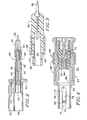
- Fig. 1 is a perspective view of the measurement probe according to the present invention.
- Fig. 2 is a cross-sectional view along the axis of the signal input head of the measurement probe according to the present invention.
- Fig. 3 is a cross-sectional view along the axis of the signal input head of the insulating plug of the measurement probe according to the present invention.
- Fig. 4 is a cross-sectional view along the axis of the removable adapter for use with the measurement probe according to the present invention.
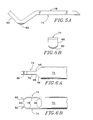
- Fig. 5A is a side view of the spring biased fingers on the removable adapter according to the present invention.
- Fig. 5B is an end view of the spring biased finger on the removable adapter according to the present invention
- Fig. 6A is a top view of an alternative sleeve structure for the removable adapter according to the present invention.
- Fig. 6B is a side view of the alternative sleeve structure for the removable adapter according to the present invention.
- Referring to Figs. 1-3, there is shown a
measurement probe 10 having asignal input head 12 connected to atermination output coupler 14 via a transmission line, or cable, 16. Thetermination output coupler 14 is connected to aninput connector 18 on anoscilloscope 20 or other type of electrical test equipment. Theoscilloscope 20 has the capability of performing floating measurements where the common voltage connection for themeasurement probe 10 is not connected to electrical ground. In an application of this type, thetermination output coupler 14 is insulated from the chassis of the instrument as well as being insulated from a user. - The
probe head 12 has aprobe tip 30 axially disposed within a plug of insulatingmaterial 32 with the probe tip extending beyond the ends of the insulatingplug 32. One end of theprobe tip 30 is used for probing a device under test while the other end is electrically connected to asubstrate 34 having electrical circuitry formed thereon. Thesubstrate 34 is disposed within an elongate electricallyconductive tube 36 that forms the outer coaxial conductor of thesignal input head 12 of themeasurement probe 10. An insulatingmaterial 38 surrounds thesubstrate 34 to prevent electrical arcing between thesubstrate 34 and theconductive tube 36. The other end of thesubstrate 34 is electrically connected to anelectrical jack 42 that accepts a mating electrical plug (not shown) on the end of thetransmission line 16. Theconductive tube 36 fits within aslot 40 formed in the insulatingplug 32. - Angularly depending and electrically connected to the
conductive tube 36 is anelectrical conductor 44 that is used for connecting the conductive tube to an electrical source for floating measurements or electrical ground for ground referenced measurements. Thesignal input head 12 is covered by an insulatingmaterial 46 that provides the shape for thesignal input head 12 and electrically isolates theconductive tube 36 from the user.Electrical jack 42 andelectrical connector 44 are respectively exposed withinapertures material 46 of thesignal input head 12. Afinger guard 52 extends radially around thesignal input head 12 and is positioned away from theprobe tip 30 to provide additional protection for the user. The above described measurement probe has been described with an insulatingplug 32 and insulatingmaterial 46 surrounding thesignal input head 12. These elements may be formed as a single element having the structure described above and here in after without departing from the scope of the invention as set forth in the appended claims. - The above described
measurement probe 10 may be used for making floating measurements where the outerconductive tube 36 is connected to an electrical source, such as one of the voltage phases of a three phase electrical power source. In order to provide the necessary protection for the user and the testing equipment while making such measurements, themeasurement probe 10 must meet the electrical and electronic measuring and test equipment standards (UL1244) set by Under- vriters Laboratories, UL, for minimum distances between conductive elements and between conductive elements and the user for particular voltage ratings. In the preferred embodiment of the present invention, themeasurement probe 10 has an AC peak voltage rating of 850 volts. To meet the UL standards for safety, there needs to be a minimum separation between conductive elements within themeasurement probe 10 and between the user and any exposed conductive element in theprobe 10 of .240 inches through air and .360 inches over surfaces. To meet these standards, the insulatingplug 32 into which theprobe tip 30 is axially disposed is formed withcentral aperture 54 in which theprobe tip 30 is exposed, as shown in Fig. 3. Surrounding the central aperture is an inner sleeve 56 which in conjunction with anouter sleeve 58 definesslot 40 into which theconductive tube 36 slidably fits. The distance between theprobe tip 30 exposed within thecentral aperture 54 and the outer edge of theinner sleeve 58 meets the minimum over surface separation set by Underwriters Laboratories. Likewise, the over surface distance and the through air distance between the end ofaperture 50 and theelectrical conductor 44 are greater than the minimums set by the UL standards for ameasurement probe 10 rated at 850 peak AC volts. Further, theprobe 10 meets the standard for double insulated probes, which is 4 times the peak voltage rating of the probe plus 2,878 peak AC volts during 60 Hz high voltage testing. This is equal to 6,228 peak AC volts or approximately 12KV peak-to-peak. The above described probe structure also meets the Institute of Electrical and Electronic Engineers probe tip rating standards IEEE 587 for transient surges, which are equivalent to the UL double insulation standards. - While the above described probe meets the standards for a measurement probe for floating high voltage measurements, it does not provide an electrical connection for removable adapters needing a ground referenced coaxial signal path. This is because the outer conductor, in the form of the
conductive tube 36, is completely insulated from the user, whereas in conventional measurement probes like the low voltage probes previously described, the outer conductor is exposed near the probe tip for accepting a removable adapter, such as the BNC adapter previously described. To provide for a ground referenced coaxial signal path,notches 60 are formed in the insulatingmaterial 46 to expose theconductive tube 36 at a safe distance from theprobe tip 30. Alternatively, thenotches 60 may be formed in the plug of insulatingmaterial 32. Thenotches 60 provide a means for electrically connecting anouter conductor 64 of aremovable adapter 62 to theconductive tube 36. As is shown in Figs. 1, 4 and 5A-B, theremovable adapter 62 has a BNC typeelectrical connector 66 having anouter conductor 68 and acentral conductor 70 at one end and a electrically conductivetubular sleeve 72 at the other.Sleeve 72 defines abore 73 into which themeasurement probe 10 is inserted. Springbiased fingers 74 are disposed withinslots 76 formed insleeve 72 for engaging thenotch 60 in the insulatingmaterial 46 of thesignal input head 12 of themeasurement probe 10 to make electrical contact withconductive tube 36 of theprobe 10. The springbiased fingers 74 have integrally formed first and second segments, respectively numbered 78 and 80, with one end of the first segment integrally formed withsleeve 72. To reduce the mechanical stresses between the springbiased fingers 74 andsleeve 72, the interconnections betweensegments 78 and thesleeve 72 are formed with aradius 75 that is a minimum of one forth the width of the spring biased fingers. The second segment angularly depends from the other end of the first segment into thebore 73 region and has a dome shapedapex 82 to prevent gouging of the insulatingmaterial 46 during placement of theremovable adapter 62 on themeasurement probe 10. In production manufacturing of thesleeve 72 with the springbiased fingers 74, a stamping process may be used to cut parallel slots in the sleeve and then deform the metal between the slots into the springbiased fingers 74. -
Sleeve 72 has aflange 84 formed at one end that mates with ashoulder 86 formed in theouter conductor 68 of theBNC type connector 66. Thecenter conductor 70 has ajack 88 at one end that is electrically insulated from theouter conductor 68 by insulatingmaterial 90. The other end of the central conductor is electrically insulated from theouter conductor 68 by insulatingmaterial 92 and forms a probingtip 94 that is coupled to a device under test for coupling voltages to themeasurement probe 10. - The
bore 73 of thetubular sleeve 72 allows theremovable adapter 62 to slidably mate with thesignal input head 12 of themeasurement probe 10. The springbiased fingers 74 on thetubular sleeve 72 engage thenotches 60 in the insulatingmaterial 46 to make electrical contact with theconductive tube 36. At the same time theprobe tip 30 engages thejack 88 in theremovable adapter 62 providing the electrical connection to the probingtip 94. - The
removable adapter 62 has been described with a BNC typeelectrical conductor 66. Other types of electrical connectors or devices may be used with theremovable adapter 62 of the present invention without departing from the scope of the invention as defined in the appended claims and equivalents thereof so long as theremovable adapter 62 has spring biasedfingers 74 for engaging the notch in themeasurement probe 10 and a jack for electrically connecting to the probe tip of theprobe 10. Other type of coaxial electrical connectors include SMA connectors, UHF, RCA and the like. Alternatively, the probing tip of theremovable adapter 62 may be a current or temperature sensing device. - An alternative structure for the
removable adapter 62 is shown in Figs. 6A-B. Instead of formingslots 76 within thesleeve 72 of theouter conductor 68 with the springbiased fingers 74 disposed within the slots, the sleeve is formed with approximately triangular shapedprotrusions 96 extending axially from the end of thesleeve 72. Extending from the apex of the triangular shapedprotrusions 96 are the springbiased fingers 74. The springbiased fingers 74 have the same structure as the fingers in the previously described embodiment. The base and the height dimensions of the triangular shapedprotrusion 96 are selected as a function of the amount of force to be applied by the springbiased fingers 74 at the domed shapedapex 82 ofsegment 80. For example, to increase the spring force of the springbiased fingers 74, the height of the triangular shapedprotrusion 96 is increased at the expense of the length ofsegment 78 of the springbiased fingers 74. Further, to reduce stress concentrations at the interconnection of thefirst segment 78 and the apex of the triangular shapedprotrusion 96, aradius 98 is formed at the interconnection that is a minimum of one forth the width of the springbiased fingers 72. - A measurement probe has been described having a elongate cylindrical outer conductor with a coaxially disposed probe tip extending beyond one end of the outer conductor. A body of insulating material surrounds the outer conductor and a portion of the probe tip to provide electrical isolation between the probe tip and the outer conductor. A notch is formed in the insulating material distant from the probe tip for exposing the outer conductor to provide a means for electrically connecting an outer conductor of a removable adapter to the outer conductor of the measurement probe. The removable adapter has a tubular sleeve that slidably mates with the measurement probe and has spring biased fingers formed therein for engaging the notch in the insulating material to make electrical contact with the outer conductor of the measurement probe. A central conductor disposed within the removable adapter has a jack formed on one end thereof for making electrical contact with the probe tip of the measurement probe. The measurement probe meets all the safety standards for floating measurements while at the same time having the capability providing a ground referenced coaxial signal path for ground referenced signal measurements. These and other aspects of the present invention are set forth in the appended claims.
Claims (19)
Applications Claiming Priority (2)
| Application Number | Priority Date | Filing Date | Title |
|---|---|---|---|
| US647315 | 1991-01-29 | ||
| US07/647,315 US5136237A (en) | 1991-01-29 | 1991-01-29 | Double insulated floating high voltage test probe |
Publications (3)
| Publication Number | Publication Date |
|---|---|
| EP0496984A2 true EP0496984A2 (en) | 1992-08-05 |
| EP0496984A3 EP0496984A3 (en) | 1993-06-02 |
| EP0496984B1 EP0496984B1 (en) | 1997-03-12 |
Family
ID=24596477
Family Applications (1)
| Application Number | Title | Priority Date | Filing Date |
|---|---|---|---|
| EP91120991A Expired - Lifetime EP0496984B1 (en) | 1991-01-29 | 1991-12-06 | Measurement probe |
Country Status (4)
| Country | Link |
|---|---|
| US (1) | US5136237A (en) |
| EP (1) | EP0496984B1 (en) |
| JP (1) | JPH087231B2 (en) |
| DE (1) | DE69125136T2 (en) |
Cited By (2)
| Publication number | Priority date | Publication date | Assignee | Title |
|---|---|---|---|---|
| GB2315169A (en) * | 1996-07-10 | 1998-01-21 | Hewlett Packard Co | Probe adapter with slotted body |
| WO2000039595A1 (en) * | 1998-12-30 | 2000-07-06 | Proteus Corporation | Dual-pin probe for testing circuit boards |
Families Citing this family (45)
| Publication number | Priority date | Publication date | Assignee | Title |
|---|---|---|---|---|
| US5338213A (en) * | 1993-02-01 | 1994-08-16 | Hubbell Incorporated | Submersible pump pothead test plug |
| US6028423A (en) * | 1997-12-11 | 2000-02-22 | Sanchez; Jorge | Isolation instrument for electrical testing |
| US5729150A (en) | 1995-12-01 | 1998-03-17 | Cascade Microtech, Inc. | Low-current probe card with reduced triboelectric current generating cables |
| US5914613A (en) | 1996-08-08 | 1999-06-22 | Cascade Microtech, Inc. | Membrane probing system with local contact scrub |
| US6034533A (en) | 1997-06-10 | 2000-03-07 | Tervo; Paul A. | Low-current pogo probe card |
| US6256882B1 (en) | 1998-07-14 | 2001-07-10 | Cascade Microtech, Inc. | Membrane probing system |
| US6578264B1 (en) | 1999-06-04 | 2003-06-17 | Cascade Microtech, Inc. | Method for constructing a membrane probe using a depression |
| US6255834B1 (en) | 1999-10-21 | 2001-07-03 | Dell Usa, L.P. | Test fixture having a floating self-centering connector |
| US6466044B1 (en) | 1999-10-21 | 2002-10-15 | Dell Products L.P. | Through connector circuit test apparatus |
| US6838890B2 (en) | 2000-02-25 | 2005-01-04 | Cascade Microtech, Inc. | Membrane probing system |
| US6605934B1 (en) * | 2000-07-31 | 2003-08-12 | Lecroy Corporation | Cartridge system for a probing head for an electrical test probe |
| US6965226B2 (en) | 2000-09-05 | 2005-11-15 | Cascade Microtech, Inc. | Chuck for holding a device under test |
| US6914423B2 (en) | 2000-09-05 | 2005-07-05 | Cascade Microtech, Inc. | Probe station |
| DE20114544U1 (en) | 2000-12-04 | 2002-02-21 | Cascade Microtech Inc | wafer probe |
| WO2003052435A1 (en) | 2001-08-21 | 2003-06-26 | Cascade Microtech, Inc. | Membrane probing system |
| US6724205B1 (en) | 2002-11-13 | 2004-04-20 | Cascade Microtech, Inc. | Probe for combined signals |
| KR100449204B1 (en) * | 2002-11-25 | 2004-09-18 | 리노공업주식회사 | Air Interface Apparatus for Use in High Frequency Probe |
| ATE424640T1 (en) | 2003-01-08 | 2009-03-15 | Tecey Software Dev Kg Llc | DEVICE AND METHOD FOR MEASURING DYNAMIC LASER SIGNALS |
| US7057404B2 (en) | 2003-05-23 | 2006-06-06 | Sharp Laboratories Of America, Inc. | Shielded probe for testing a device under test |
| US7492172B2 (en) | 2003-05-23 | 2009-02-17 | Cascade Microtech, Inc. | Chuck for holding a device under test |
| US7250626B2 (en) | 2003-10-22 | 2007-07-31 | Cascade Microtech, Inc. | Probe testing structure |
| JP2007517231A (en) | 2003-12-24 | 2007-06-28 | カスケード マイクロテック インコーポレイテッド | Active wafer probe |
| US7187188B2 (en) | 2003-12-24 | 2007-03-06 | Cascade Microtech, Inc. | Chuck with integrated wafer support |
| DE202005021435U1 (en) | 2004-09-13 | 2008-02-28 | Cascade Microtech, Inc., Beaverton | Double-sided test setups |
| US7656172B2 (en) | 2005-01-31 | 2010-02-02 | Cascade Microtech, Inc. | System for testing semiconductors |
| US7535247B2 (en) | 2005-01-31 | 2009-05-19 | Cascade Microtech, Inc. | Interface for testing semiconductors |
| US20060267608A1 (en) * | 2005-05-18 | 2006-11-30 | Robert Faust | Adaptive test meter probe system and method of operation |
| JP4231038B2 (en) * | 2005-08-22 | 2009-02-25 | 株式会社ケーヒン | High voltage measuring device |
| US7294995B1 (en) * | 2006-05-08 | 2007-11-13 | Tektronix, Inc. | Current probing system |
| US7723999B2 (en) | 2006-06-12 | 2010-05-25 | Cascade Microtech, Inc. | Calibration structures for differential signal probing |
| US7764072B2 (en) | 2006-06-12 | 2010-07-27 | Cascade Microtech, Inc. | Differential signal probing system |
| US7403028B2 (en) | 2006-06-12 | 2008-07-22 | Cascade Microtech, Inc. | Test structure and probe for differential signals |
| US7876114B2 (en) | 2007-08-08 | 2011-01-25 | Cascade Microtech, Inc. | Differential waveguide probe |
| US7888957B2 (en) | 2008-10-06 | 2011-02-15 | Cascade Microtech, Inc. | Probing apparatus with impedance optimized interface |
| US8410806B2 (en) | 2008-11-21 | 2013-04-02 | Cascade Microtech, Inc. | Replaceable coupon for a probing apparatus |
| US8319503B2 (en) | 2008-11-24 | 2012-11-27 | Cascade Microtech, Inc. | Test apparatus for measuring a characteristic of a device under test |
| CN102004173B (en) * | 2009-09-01 | 2014-02-19 | 鸿富锦精密工业(深圳)有限公司 | Probe |
| US9049351B2 (en) * | 2010-05-03 | 2015-06-02 | Inspectron, Inc. | Insulator design for video inspection devices |
| TW201248178A (en) * | 2011-05-23 | 2012-12-01 | Hon Hai Prec Ind Co Ltd | Apparatus for calibrating probes |
| TW201248157A (en) * | 2011-05-24 | 2012-12-01 | Hon Hai Prec Ind Co Ltd | Apparatus for measurement probes |
| US9575091B2 (en) * | 2013-03-15 | 2017-02-21 | Kenneth Mark Reeder, III | Testing device for electrical safety using wireless communication |
| US9188606B2 (en) | 2013-04-29 | 2015-11-17 | Keysight Technologies, Inc. | Oscilloscope current probe with interchangeable range and sensitivity setting modules |
| US10119992B2 (en) | 2015-04-01 | 2018-11-06 | Tektronix, Inc. | High impedance compliant probe tip |
| US9810715B2 (en) | 2014-12-31 | 2017-11-07 | Tektronix, Inc. | High impedance compliant probe tip |
| DE102019109129A1 (en) * | 2019-04-08 | 2020-10-08 | Lisa Dräxlmaier GmbH | Contact pin for a test device for testing an electrical contact and test device |
Citations (3)
| Publication number | Priority date | Publication date | Assignee | Title |
|---|---|---|---|---|
| US4209742A (en) * | 1976-10-13 | 1980-06-24 | Tektronix, Inc. | Modular probe system |
| GB2125236A (en) * | 1982-08-11 | 1984-02-29 | Tektronix Inc | Stress-isolating electrical connections |
| EP0222119A1 (en) * | 1985-10-28 | 1987-05-20 | International Business Machines Corporation | Coaxial probe |
Family Cites Families (2)
| Publication number | Priority date | Publication date | Assignee | Title |
|---|---|---|---|---|
| JPS57151114A (en) * | 1981-03-12 | 1982-09-18 | Mitsubishi Electric Corp | Resistance welding machine |
| JPS57207865A (en) * | 1981-06-17 | 1982-12-20 | Hitachi Ltd | Measuring terminal |
-
1991
- 1991-01-29 US US07/647,315 patent/US5136237A/en not_active Expired - Lifetime
- 1991-12-06 DE DE69125136T patent/DE69125136T2/en not_active Expired - Fee Related
- 1991-12-06 EP EP91120991A patent/EP0496984B1/en not_active Expired - Lifetime
-
1992
- 1992-01-29 JP JP4038735A patent/JPH087231B2/en not_active Expired - Fee Related
Patent Citations (3)
| Publication number | Priority date | Publication date | Assignee | Title |
|---|---|---|---|---|
| US4209742A (en) * | 1976-10-13 | 1980-06-24 | Tektronix, Inc. | Modular probe system |
| GB2125236A (en) * | 1982-08-11 | 1984-02-29 | Tektronix Inc | Stress-isolating electrical connections |
| EP0222119A1 (en) * | 1985-10-28 | 1987-05-20 | International Business Machines Corporation | Coaxial probe |
Cited By (3)
| Publication number | Priority date | Publication date | Assignee | Title |
|---|---|---|---|---|
| GB2315169A (en) * | 1996-07-10 | 1998-01-21 | Hewlett Packard Co | Probe adapter with slotted body |
| GB2315169B (en) * | 1996-07-10 | 2000-07-12 | Hewlett Packard Co | Probe adaptor |
| WO2000039595A1 (en) * | 1998-12-30 | 2000-07-06 | Proteus Corporation | Dual-pin probe for testing circuit boards |
Also Published As
| Publication number | Publication date |
|---|---|
| EP0496984A3 (en) | 1993-06-02 |
| DE69125136D1 (en) | 1997-04-17 |
| JPH0682480A (en) | 1994-03-22 |
| JPH087231B2 (en) | 1996-01-29 |
| EP0496984B1 (en) | 1997-03-12 |
| DE69125136T2 (en) | 1997-10-09 |
| US5136237A (en) | 1992-08-04 |
Similar Documents
| Publication | Publication Date | Title |
|---|---|---|
| US5136237A (en) | Double insulated floating high voltage test probe | |
| JP3172690B2 (en) | Connection device between measuring device and test lead | |
| US7909613B2 (en) | Coaxial connecting device | |
| US7015709B2 (en) | Ultra-broadband differential voltage probes | |
| US5490033A (en) | Electrostatic discharge protection device | |
| US7015708B2 (en) | Method and apparatus for a high frequency, impedance controlled probing device with flexible ground contacts | |
| US6175080B1 (en) | Strain relief, pull-strength termination with controlled impedance for an electrical cable | |
| KR100855208B1 (en) | High performance tester interface module | |
| AU2006252207A1 (en) | Separable electrical connector component having a voltage output branch and a direct access point | |
| KR950006472A (en) | Probe card, coaxial probe beam for probe card and manufacturing method thereof | |
| US6992495B2 (en) | Shielded probe apparatus for probing semiconductor wafer | |
| JPH0127101Y2 (en) | ||
| US11099215B2 (en) | Sensor with discrete impedance elements for high voltage connectors | |
| US5061892A (en) | Electrical test probe having integral strain relief and ground connection | |
| US5808475A (en) | Semiconductor probe card for low current measurements | |
| TWI700500B (en) | Test device | |
| US5488313A (en) | Test probe and circuit board arrangement for the circuit under test for microstrip circuitry | |
| CA1098984A (en) | Low-profile test clip adapter | |
| JP2944677B2 (en) | Conductive contact | |
| KR102447286B1 (en) | Adaptor for cable | |
| CN114207952B (en) | Inspection probe device and connector inspection method | |
| TWI837645B (en) | Cable adaptor | |
| GB2336948A (en) | BNC test connector | |
| EP0406192A1 (en) | A connecting device for coaxial conductors | |
| JPH0427873A (en) | Probe |
Legal Events
| Date | Code | Title | Description |
|---|---|---|---|
| PUAI | Public reference made under article 153(3) epc to a published international application that has entered the european phase |
Free format text: ORIGINAL CODE: 0009012 |
|
| AK | Designated contracting states |
Kind code of ref document: A2 Designated state(s): DE FR GB IT |
|
| PUAL | Search report despatched |
Free format text: ORIGINAL CODE: 0009013 |
|
| AK | Designated contracting states |
Kind code of ref document: A3 Designated state(s): DE FR GB IT |
|
| 17P | Request for examination filed |
Effective date: 19930915 |
|
| 17Q | First examination report despatched |
Effective date: 19950330 |
|
| GRAG | Despatch of communication of intention to grant |
Free format text: ORIGINAL CODE: EPIDOS AGRA |
|
| RAP1 | Party data changed (applicant data changed or rights of an application transferred) |
Owner name: TEKTRONIX, INC. |
|
| GRAH | Despatch of communication of intention to grant a patent |
Free format text: ORIGINAL CODE: EPIDOS IGRA |
|
| GRAH | Despatch of communication of intention to grant a patent |
Free format text: ORIGINAL CODE: EPIDOS IGRA |
|
| GRAA | (expected) grant |
Free format text: ORIGINAL CODE: 0009210 |
|
| AK | Designated contracting states |
Kind code of ref document: B1 Designated state(s): DE FR GB IT |
|
| REF | Corresponds to: |
Ref document number: 69125136 Country of ref document: DE Date of ref document: 19970417 |
|
| ITF | It: translation for a ep patent filed |
Owner name: SOCIETA' ITALIANA BREVETTI S.P.A. |
|
| ET | Fr: translation filed | ||
| PLBE | No opposition filed within time limit |
Free format text: ORIGINAL CODE: 0009261 |
|
| STAA | Information on the status of an ep patent application or granted ep patent |
Free format text: STATUS: NO OPPOSITION FILED WITHIN TIME LIMIT |
|
| 26N | No opposition filed | ||
| REG | Reference to a national code |
Ref country code: GB Ref legal event code: IF02 |
|
| PGFP | Annual fee paid to national office [announced via postgrant information from national office to epo] |
Ref country code: FR Payment date: 20031110 Year of fee payment: 13 |
|
| PGFP | Annual fee paid to national office [announced via postgrant information from national office to epo] |
Ref country code: GB Payment date: 20031118 Year of fee payment: 13 |
|
| PGFP | Annual fee paid to national office [announced via postgrant information from national office to epo] |
Ref country code: DE Payment date: 20031125 Year of fee payment: 13 |
|
| PG25 | Lapsed in a contracting state [announced via postgrant information from national office to epo] |
Ref country code: GB Free format text: LAPSE BECAUSE OF NON-PAYMENT OF DUE FEES Effective date: 20041206 |
|
| PG25 | Lapsed in a contracting state [announced via postgrant information from national office to epo] |
Ref country code: DE Free format text: LAPSE BECAUSE OF NON-PAYMENT OF DUE FEES Effective date: 20050701 |
|
| GBPC | Gb: european patent ceased through non-payment of renewal fee |
Effective date: 20041206 |
|
| PG25 | Lapsed in a contracting state [announced via postgrant information from national office to epo] |
Ref country code: FR Free format text: LAPSE BECAUSE OF NON-PAYMENT OF DUE FEES Effective date: 20050831 |
|
| REG | Reference to a national code |
Ref country code: FR Ref legal event code: ST |
|
| PG25 | Lapsed in a contracting state [announced via postgrant information from national office to epo] |
Ref country code: IT Free format text: LAPSE BECAUSE OF NON-PAYMENT OF DUE FEES;WARNING: LAPSES OF ITALIAN PATENTS WITH EFFECTIVE DATE BEFORE 2007 MAY HAVE OCCURRED AT ANY TIME BEFORE 2007. THE CORRECT EFFECTIVE DATE MAY BE DIFFERENT FROM THE ONE RECORDED. Effective date: 20051206 |