EP0492337A2 - Device for determining programmed states of fuses - Google Patents
Device for determining programmed states of fuses Download PDFInfo
- Publication number
- EP0492337A2 EP0492337A2 EP91121514A EP91121514A EP0492337A2 EP 0492337 A2 EP0492337 A2 EP 0492337A2 EP 91121514 A EP91121514 A EP 91121514A EP 91121514 A EP91121514 A EP 91121514A EP 0492337 A2 EP0492337 A2 EP 0492337A2
- Authority
- EP
- European Patent Office
- Prior art keywords
- negator
- programming
- transistor
- supply voltage
- node
- Prior art date
- Legal status (The legal status is an assumption and is not a legal conclusion. Google has not performed a legal analysis and makes no representation as to the accuracy of the status listed.)
- Withdrawn
Links
Images
Classifications
-
- G—PHYSICS
- G11—INFORMATION STORAGE
- G11C—STATIC STORES
- G11C17/00—Read-only memories programmable only once; Semi-permanent stores, e.g. manually-replaceable information cards
- G11C17/14—Read-only memories programmable only once; Semi-permanent stores, e.g. manually-replaceable information cards in which contents are determined by selectively establishing, breaking or modifying connecting links by permanently altering the state of coupling elements, e.g. PROM
- G11C17/18—Auxiliary circuits, e.g. for writing into memory
Definitions
- the invention relates to a circuit arrangement for detecting the programming state of burnout elements according to the preamble of claim 1. It can be used in static and dynamic semiconductor memories with random access, which have redundant structures that can be activated by means of programmed burnout elements.
- Redundancy structures are used to increase the yield in the manufacture of integrated RAM memory circuits. These are deliberately built-in additional elements that take over the function of defective elements if necessary. With the redundancy structures, point defects can be corrected, the effects of which only capture a small part of the memory; So cell failures, bit and word line failures of different sizes and combinations thereof. Since the redundancy structures are only used when errors occur, each element must have a programmable logic that realizes the assignment of a redundant structure to the separated defective structure. This is usually done using so-called redundancy decoders.
- 90 332 and 120 485 is the valuation of the Conductivity of the burn-through elements together, that the fuse resistance is significantly lower in the non-programmed state than in the programmed one. A relatively large forbidden resistance range is defined between the two states for reliable detection. So the fuse detection circuit according to EP application. 290 094 a controllable voltage divider connected between supply and reference voltage potential from the fuse and a discharge transistor. The node between them is fed back to the control electrode of the discharge transistor via a negator. The output of the negator carries the signal about the programming state of the fuse and at the same time controls the discharge of the named node. For electrical programming, a programming transistor is also connected in parallel with the discharge transistor, the control electrode of which is connected to an output of a programming decoder.
- a programming voltage is applied to the connection of the fuse.
- the burn-through elements can still have a residual conductivity, which is caused by layers that have not been completely removed and is in the prohibited area.
- the switching threshold of the downstream evaluation circuit for a non-programmed blowout element in the voltage divider can be exceeded, so that the otherwise correctly programmed blowout element is incorrectly evaluated. Accordingly, there is no assignment of redundancy structures to the defective addresses, so that the circuit in question cannot be obtained without errors despite redundancy programming.
- the invention has for its object to provide a circuit arrangement for detecting the programming state of blow-through elements, preferably in redundancy decoders, which enables the reliable determination of the programming state even with a higher residual conductivity of the programmed burn-through element, so that an increase the yield in the redundancy repair of static and dynamic semiconductor memories with random access, which are manufactured in particular in CMOS technology, where the programming of the redundant structures is carried out using burn-through elements.
- the object is achieved by a circuit arrangement with the features of claim 1.
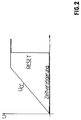
- the supply voltage of a circuit which contains the circuit arrangement according to the invention is switched on, it rises only slowly to the full value due to the total capacitance of the circuit. After reaching this value and possibly a further time delay, the reset signal jumps.
- the node at the output of the negator which represents the output of the circuit arrangement according to the invention, is charged via said transistor of the second conductivity type, so that the output of the circuit arrangement reliably leads to the level of the supply voltage when switched on.
- the discharge transistor is conductive, which creates a potential at the input of the negator, which is determined by the series resistor, the resistance of the blow-through element and the resistance of the open-controlled discharge transistor.
- the transistor inserted according to the invention brings about a safe preferred position of the negator when switched on.
- the programming status of the burn-through elements to be assessed can also be reliably determined in the case of a residual conductivity after programming, the remaining prohibited resistance range being orders of magnitude smaller than in the previously known solutions.
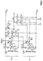
- the circuit arrangement 1.0 and 1.n each contain a series circuit comprising a series resistor 2, the blow-through element 3 and an nMOS discharge transistor 4, which are arranged between a supply voltage potential U CC and a reference potential U SS .
- a node K1 between the blow-through element 3 and the discharge transistor 4 is connected to the input of an inverter 5, the output of which as a node K2 represents the output of the circuit arrangement 1.0 or 1.n.
- the output of the negator 5 is led to the control electrode of the discharge transistor 4.
- a pMOS transistor 6 is connected between the supply voltage potential U CC and the node K2, and a reset signal RESET is applied to its control electrode.
- the reset signal RESET is generated in a circuit, not shown, when the supply voltage of the circuit is switched on. It is implemented as a step function which is delayed in comparison with the switch-on function of the supply voltage.
- the reset signal RESET now switches from low (U SS ) to high level (U CC ) only after this final value has been reached and a further delay time.
- the total time delay is chosen so large that the reset signal RESET only becomes active when the supply voltage inside the circuit safely carries the value of U CC .
- the time course of the reset signal RESET is shown again in FIG. 2.
- a programming transistor 7 is connected to the reference potential U SS at the node K1 of the circuit arrangements 1.0 or 1.n, that is to say in parallel with the discharge transistor 4.
- the control electrode of the programming transistor 7 is connected to an associated output of a programming decoder, which is not shown. Furthermore, a connection for a programming voltage U pr is provided at the node K3 between the series resistor 2 and the blow-through element 3. The series resistor 2 takes over the decoupling from the supply voltage potential U CC and the potential of the programming voltage U pr .
- the node K2 of the circuit arrangement 1.0 is led via a negator 8 to the input of a clocked negator 9. This consists of a series connection of two pMOS transistors 9.1; 9.2 and an nMOS transistor 9.3, which are arranged between the operating voltage potential U CC and the reference potential U SS .
- the interconnected control electrodes of transistors 9.2; 9.3 the input of the negator 9; a precharge clock T V is applied to the control electrode of transistor 9.1.
- the output of the negator 9 is specified as node K4 and represents the output of the redundancy decoder to a redundant address.
- a pMOS transistor 10 is connected between the supply voltage potential U CC and the node K4. Its control electrode is connected to node K4 via a negator 11.
- the transistor 10 serves to keep the high level active after the node K4 has been charged via the Precharge cycle T V. Between the node K4 and the reference potential U SS there are 2n series connections of two nMOS transistors 12.n; 13.n and 14.n; 15.n arranged.
- the nodes K2 as outputs of the circuit arrangements 1.n are connected to the control electrodes of the transistors 12.n and the associated nodes K2 are also connected to the control electrodes of the transistors 14.n, but in each case via a negator 16.n.
- the true addresses An are routed to the control electrodes of the transistors 13.n and the negated addresses / An are routed to the control electrodes of the transistors 15.n. Only for a certain address combination of addresses To; /
- the node K4 of the redundancy decoder is not unloaded and the node K4 can be evaluated in the redundancy decoder in the manner described.
Abstract
Description
Die Erfindung betrifft eine Schaltungsanordnung zur Erkennung des Programmierzustandes von Durchbrennelementen nach dem Oberbegriff des Anspruches 1. Sie ist in statischen und dynamischen Halbleiterspeichern mit wahlfreiem Zugriff, welche über vermittels programmierter Durchbrennelemente zuschaltbare redundante Strukturen verfügen, einsetzbar.The invention relates to a circuit arrangement for detecting the programming state of burnout elements according to the preamble of claim 1. It can be used in static and dynamic semiconductor memories with random access, which have redundant structures that can be activated by means of programmed burnout elements.
Zur Ausbeuteerhöhung bei der Herstellung integrierter RAM-Speicherschaltkreise werden Redundanzstrukturen eingesetzt. Dabei handelt es sich um bewußt eingebaute Zusatzelemente, die im Bedarfsfall die Funktion defekter Elemente übernehmen.
Mit den Redundanzstrukturen lassen sich Punktdefekte korrigieren, welche in ihren Auswirkungen nur einen kleinen Teil des Speichers erfassen; also Zellausfälle, Bit- und Wortleitungsausfälle unterschiedlichen Umfanges und Kombinationen hiervon.
Da die Redundanzstrukturen nur genutzt werden, wenn Fehler auftreten, muß jedes Element über eine programmierbare Logik verfügen, welche die Zuweisung einer redundanten Struktur zur abgetrennten defekten Struktur realisiert. Dies erfolgt üblicherweise über sogenannte Redundanzdekoder.
Als Programmiertechnik hat sich dabei die Zerstörung von Leitbahnelementen, den "Durchbrennelementen", auch als "fusible links" oder "fuse" bezeichnet, mittels Laserstrahl oder elektrischer Impulse (überhöhte Leistung) allgemein durchgesetzt.
Entsprechende Lösungen sind u. a. aus der US-PS 4.047.163 bzw. aus Fitzgerald, B. F.; Thoma, E. P.: "Circuit Implementation of Fusible Redundant Adresses on RAM's for Productivity Enhancement"; IBM Journal of Research and Developement; Vol. 24 Nr. 3, pp. 291-95 bekannt.
Die Programmierung der redundanten Strukturen greift dabei auf Schaltungen zurück, welche den Programmierzustand der Durchbrennelemente erkennen bzw. bewerten.
Diesen sogenannten "Fuseerkennungsschaltungen", dargelegt u. a. in den EP-Anm. 90 332 und 120 485, ist die Bewertung der Leitfähigkeit der Durchbrennelemente gemeinsam, daß der Fusewiderstand im nichtprogrammierten Zustand wesentlich geringer ist als im programmierten. Zum sicheren Erkennen ist zwischen den beiden Zuständen ein relativ großer verbotener Widerstandsbereich festgelegt.
So verwendet die Fuseerkennungsschaltung nach EP-Anm. 290 094 einen zwischen Versorgungs- und Bezugsspannungspotential geschalteten steuerbaren Spannungsteiler aus dem Fuse und einem Entladetransistor. Dabei ist der Knoten zwischen ihnen über einen Negator auf die Steuerelektrode des Entladetransistors rückgekoppelt.
Der Ausgang des Negators führt hierbei das Signal über den Programmierzustand des Fuse und steuert gleichzeitig die Entladung des genannten Knotens.
Für eine elektrische Programmierung ist dem Entladetransistor noch ein Programmiertransistor parallelgeschaltet, dessen Steuerelektrode an einem Ausgang eines Programmierdekoders angeschlossen ist. Eine Programmierspannung wird an den Anschluß des Fuse gelegt.
Nach dem Programmieren können die Durchbrennelemante jedoch noch eine Restleitfähigkeit besitzen, welche durch nicht restlos entfernte Schichten hervorgerufen wird und im verbotenen Bereich liegt.
In den bekannten Fuseerkennungsschaltung kann bei einer solchen Restleitfähigkeit die Schaltschwelle der nachgeordneten Auswerteschaltung für ein nichtprogrammiertes Durchbrennelement in dem Spannungsteiler überschritten werden, so daß eine fehlerhafte Auswertung des ansonsten richtig programmierten Durchbrennelementes erfolgt.
Dementsprechend erfolgt keine Zuordnung von Redundanzstrukturen zu den defekten Adressen, so daß der betreffende Schaltkreis trotz Redundanzprogrammierung nicht fehlerfrei zu erhalten ist.Redundancy structures are used to increase the yield in the manufacture of integrated RAM memory circuits. These are deliberately built-in additional elements that take over the function of defective elements if necessary.
With the redundancy structures, point defects can be corrected, the effects of which only capture a small part of the memory; So cell failures, bit and word line failures of different sizes and combinations thereof.
Since the redundancy structures are only used when errors occur, each element must have a programmable logic that realizes the assignment of a redundant structure to the separated defective structure. This is usually done using so-called redundancy decoders.
The destruction of interconnect elements, the "blow-through elements", also referred to as "fusible links" or "fuse", by means of laser beams or electrical impulses (excessive power) has become generally accepted as programming technology.
Corresponding solutions are, inter alia, from US Pat. No. 4,047,163 or from Fitzgerald, BF; Thoma, EP: "Circuit Implementation of Fusible Redundant Addresses on RAM's for Productivity Enhancement"; IBM Journal of Research and Development; Vol. 24 No. 3, pp. 291-95 known.
The programming of the redundant structures uses circuits that recognize or evaluate the programming status of the burn-through elements.
These so-called "fuse detection circuits", set forth inter alia in EP application. 90 332 and 120 485, is the valuation of the Conductivity of the burn-through elements together, that the fuse resistance is significantly lower in the non-programmed state than in the programmed one. A relatively large forbidden resistance range is defined between the two states for reliable detection.
So the fuse detection circuit according to EP application. 290 094 a controllable voltage divider connected between supply and reference voltage potential from the fuse and a discharge transistor. The node between them is fed back to the control electrode of the discharge transistor via a negator.
The output of the negator carries the signal about the programming state of the fuse and at the same time controls the discharge of the named node.
For electrical programming, a programming transistor is also connected in parallel with the discharge transistor, the control electrode of which is connected to an output of a programming decoder. A programming voltage is applied to the connection of the fuse.
After programming, however, the burn-through elements can still have a residual conductivity, which is caused by layers that have not been completely removed and is in the prohibited area.
In the known fuse detection circuit, with such a residual conductivity, the switching threshold of the downstream evaluation circuit for a non-programmed blowout element in the voltage divider can be exceeded, so that the otherwise correctly programmed blowout element is incorrectly evaluated.
Accordingly, there is no assignment of redundancy structures to the defective addresses, so that the circuit in question cannot be obtained without errors despite redundancy programming.
Der Erfindung liegt die Aufgabe zugrunde, eine Schaltungsanordnung zur Erkennung des Programmierzustandes von Durchbrennelementen, vorzugsweise in Redundanzdekodern, anzugeben, welche die sichere Feststellung des Programmierzustandes auch bei einer höheren Restleitfähigkeit des programmierten Durchbrennelementes ermöglicht, so daß eine Erhöhung der Ausbeute bei der Redundanzreparatur von statischen und dynamischen Halbleiterspeichern mit wahlfreiem Zugriff, welche insbesondere in CMOS-Technologie gefertigt werden, wo die Programmierung der redundanten Strukturen über Durchbrennelemente vorgenommen wird, erreicht wird.The invention has for its object to provide a circuit arrangement for detecting the programming state of blow-through elements, preferably in redundancy decoders, which enables the reliable determination of the programming state even with a higher residual conductivity of the programmed burn-through element, so that an increase the yield in the redundancy repair of static and dynamic semiconductor memories with random access, which are manufactured in particular in CMOS technology, where the programming of the redundant structures is carried out using burn-through elements.
Erfindungsgemäß wird die Aufgabe durch eine Schaltungsanordnung mit den Merkmalen des Patentanspruches 1 gelöst. Beim Einschalten der Versorgungsspannung eines Schaltkreises, welcher die erfindungsgemäße Schaltungsanordnung enthält, steigt diese aufgrund der Gesamtkapazität des Schaltkreises nur langsam auf den vollen Wert an. Nach dem Erreichen dieses Wertes und ggf. einer weiteren Zeitverzögerung erfolgt der Sprung des Rücksetzsignales.
Der Knoten am Ausgang des Negators, welcher den Ausgang der erfindungsgemäßen Schaltungsanordnung darstellt, wird über den genannten Transistor vom zweiten Leitfähigkeitstyp aufgeladen, so daß der Ausgang der Schaltungsanordnung beim Einschalten sicher den Pegel der Versorgungsspannung führt. Der Entladetransitor ist leitfähig, womit sich am Eingang des Negators ein Potential einstellt, das durch den Vorwiderstand, den Widerstand des Durchbrennelementes und den Widerstand des offengesteuerten Entladetransistors bestimmt wird.
Bei einem nichtprogrammierten Durchbrennelement ist es so groß, daß die Spannung über dem Entladetransistor den Negator öffnet. Bei einem programmierten Durchbrennelement ist diese Spannung so gering, daß der Negator sicher nicht aufgesteuert wird.
Wird nun das Rücksetzsignal aktiv, d. h. es schaltet auf den Pegel der Versorgungsspannung um, so wird der Ausgangsknoten des Negators nicht weiter über den Transistor aufgeladen. Damit ergibt sich der Ausgangspegel des Negators aus dem Potential an seinem Eingang.According to the invention the object is achieved by a circuit arrangement with the features of claim 1. When the supply voltage of a circuit which contains the circuit arrangement according to the invention is switched on, it rises only slowly to the full value due to the total capacitance of the circuit. After reaching this value and possibly a further time delay, the reset signal jumps.
The node at the output of the negator, which represents the output of the circuit arrangement according to the invention, is charged via said transistor of the second conductivity type, so that the output of the circuit arrangement reliably leads to the level of the supply voltage when switched on. The discharge transistor is conductive, which creates a potential at the input of the negator, which is determined by the series resistor, the resistance of the blow-through element and the resistance of the open-controlled discharge transistor.
In the case of a non-programmed burn-through element, it is so large that the voltage across the discharge transistor opens the negator. In the case of a programmed burn-through element, this voltage is so low that the negator is certainly not opened.
If the reset signal becomes active, ie it switches to the level of the supply voltage, the output node of the negator is no longer charged via the transistor. The output level of the negator thus results from the potential at its input.
Vorteilhafte Ausgestaltungen der Erfindung ergeben sich aus den Patentansprüchen 2 bis 4.
Dabei sind die Ausgestaltungsvarianten nach den Patentansprüchen 3 und 4 für eine elektrische Redundanzprogrammierung konfiguriert.Advantageous embodiments of the invention emerge from
The design variants are configured according to claims 3 and 4 for electrical redundancy programming.
Der erfindungsgemäß eingefügte Transistor bewirkt eine sichere Vorzugslage des Negators beim Einschalten.
Der Programmierzustand der zu bewertenden Durchbrennelemente kann auch bei einer Restleitfähigkeit nach der Programmierung sicher festgestellt werden, wobei der verbleibende verbotene Widerstandsbereich um Größenordnungen geringer ist als bei den bisher bekannten Lösungen.The transistor inserted according to the invention brings about a safe preferred position of the negator when switched on.
The programming status of the burn-through elements to be assessed can also be reliably determined in the case of a residual conductivity after programming, the remaining prohibited resistance range being orders of magnitude smaller than in the previously known solutions.
Die Erfindung sei nunmehr in einem Ausführungsbeispiel anhand zweier Zeichnungen näher erläutert.
Dabei zeigen:
- Fig. 1
- einen Redundanzdekoder mit der erfindungsgemäßen Schaltungsanordnung für das Hauptdurchbrennelement und ein Adreßdurchbrennelement
- Fig. 2
- den zeitlichen Verlauf des Rücksetzsignales.
Show:
- Fig. 1
- a redundancy decoder with the circuit arrangement according to the invention for the main blow-through element and an address blow-through element
- Fig. 2
- the time course of the reset signal.
In Fig. 1 ist ein Redundanzdekoder mit einer Schaltungsanordnung 1.0 zur Erkennung des Programmierzustandes des Hauptdurchbrennelementes und einer solchen Schaltungsanordnung 1.n für ein Adreßdurchbrennelement, welche gleich aufgebaut sind, dargestellt.
Die Schaltungsanordnungen 1.0 bzw. 1.n enthalten jeweils eine Reihenschaltung aus einem Vorwiderstand 2, dem Durchbrennelement 3 und einem nMOS-Entladetransistor 4, die zwischen einem Versorgungsspannungspotential UCC und einem Bezugspotential USS angeordnet sind. Ein Knoten K1 zwischen dem Durchbrennelement 3 und dem Entladetransistor 4 ist mit dem Eingang eines Negators 5 verbunden, dessen Ausgang als ein Knoten K2 den Ausgang der Schaltunganordnung 1.0 bzw. 1.n darstellt. Gleichzeitig ist der Ausgang des Negators 5 auf die Steuerelektrode des Entladetransistors 4 geführt.
Zwischen dem Versorgungsspannungspotential UCC und dem Knoten K2 ist ein pMOS-Transistor 6 geschaltet, an dessen Steuerelektrode ein Rücksetzsignal RESET gelegt ist.
Das Rücksetzsignal RESET wird in einer nicht dargestellten Schaltung beim Einschalten der Versorgungsspannung des Schaltkreises generiert. Es ist als eine gegenüber der Einschaltfunktion der Versorgungsspannung zeitverzögerte Sprungfunktion realisiert.1 shows a redundancy decoder with a circuit arrangement 1.0 for recognizing the programming state of the main blow-through element and such a circuit arrangement 1.n for an address blow-through element, which have the same structure.
The circuit arrangements 1.0 and 1.n each contain a series circuit comprising a
A
The reset signal RESET is generated in a circuit, not shown, when the supply voltage of the circuit is switched on. It is implemented as a step function which is delayed in comparison with the switch-on function of the supply voltage.
Beim Einschalten der Versorgungsspannung steigt diese aufgrund der hohen Gesamtkapazität des Schaltkreises nur langsam auf den endgültigen Wert an. Das Rücksetzsignal RESET schaltet nun erst nach Erreichen dieses endgültigen Wertes und einer weiteren Verzögerungszeit sprunghaft von Low-(USS) auf High-Pegel (UCC) um. Die gesamte Zeitverzögerung ist dabei so groß gewählt, daß das Rücksetzsignal RESET erst aktiv wird, wenn die Versorgungsspannung im Innern des Schaltkreises sicher den Wert von UCC führt.
Der zeitliche Verlauf des Rücksetzsignales RESET ist noch einmal in Fig. 2 gezeigt.
Für eine elektrische Redundanzprogrammierung, d. h. das Programmieren der Durchbrennelemente 4, ist am Knoten K1 der Schaltungsanordnungen 1.0 bzw. 1.n ein Programmiertransistor 7 gegen das Bezugspotential USS, also parallel zum Entladetransistor 4, geschaltet. Die Steuerelektrode des Programmiertransistors 7 ist an einem zugehörigen Ausgang eines Programmierdekoders, welcher nicht dargestellt ist, angeschlossen.
Weiterhin ist am Knoten K3 zwischen dem Vorwiderstand 2 und dem Durchbrennelement 3 ein Anschluß für eine Programmierspannung Upr vorgesehen. Der Vorwiderstand 2 übernimmt dabei die Entkopplung vom Versorgungsspannungspotential UCC und dem Potential der Programmierspannung Upr.
Der Knoten K2 der Schaltungsanordnung 1.0 ist über einen Negator 8 auf den Eingang eines getakteten Negators 9 geführt. Dieser besteht aus einer Reihenschaltung zweier pMOS-Transistoren 9.1; 9.2 und eines nMOS-Transistors 9.3, welche zwischen dem Betriebsspannungspotential UCC und dem Bezugspotential USS angeordnet sind. Dabei bilden die miteinander verbundenen Steuerelektroden der Transistoren 9.2; 9.3 den Eingang des Negators 9; an die Steuerelektrode des Transistors 9.1 ist ein Vorladetakt TV gelegt. Der Ausgang des Negators 9 ist als Knoten K4 angegeben und stellt den Ausgang des Redundanzdekoders zu einer redundanten Adresse dar. Zwischen dem Versorgungsspannungspotential UCC und dem Knoten K4 ist ein pMOS-Transistor 10 geschaltet. Seine Steuerelektrode ist, geführt über einen Negator 11, am Knoten K4 angeschlossen. Der Transistor 10 dient zum aktiven Halten des High-Pegels nach dem Aufladen des Knotens K4 über den Vorladetakt TV.
Zwischen dem Knoten K4 und dem Bezugspotential USS sind 2n Reihenschaltungen zu je zwei nMOS-Transistoren 12.n; 13.n bzw. 14.n; 15.n angeordnet.
Dabei sind an die Steuerelektroden der Transistoren 12.n die Knoten K2 als Ausgänge der Schaltungsanordnungen 1.n und an die Steuerelektroden der Transistoren 14.n ebenfalls die zugehörigen Knoten K2, jedoch jeweils über einen Negator 16.n, gelegt.
Auf die Steuerelektroden der Transistoren 13.n sind die wahren Adressen An und auf die Steuerelektroden der Transistoren 15.n die negierten Adressen /An geführt.
Nur bei einer bestimmten Adreßkombination der Adressen An; /An wird der Knoten K4 des Redundanzdekoders nicht entladen und es kann die Auswertung des Knotens K4 im Redundanzdekoder in der beschriebenen Art und Weise erfolgen.When the supply voltage is switched on, it rises only slowly to the final value due to the high total capacitance of the circuit. The reset signal RESET now switches from low (U SS ) to high level (U CC ) only after this final value has been reached and a further delay time. The total time delay is chosen so large that the reset signal RESET only becomes active when the supply voltage inside the circuit safely carries the value of U CC .
The time course of the reset signal RESET is shown again in FIG. 2.
For electrical redundancy programming, that is to say the programming of the burnout elements 4, a programming transistor 7 is connected to the reference potential U SS at the node K1 of the circuit arrangements 1.0 or 1.n, that is to say in parallel with the discharge transistor 4. The control electrode of the programming transistor 7 is connected to an associated output of a programming decoder, which is not shown.
Furthermore, a connection for a programming voltage U pr is provided at the node K3 between the
The node K2 of the circuit arrangement 1.0 is led via a
Between the node K4 and the reference potential U SS there are 2n series connections of two nMOS transistors 12.n; 13.n and 14.n; 15.n arranged.
In this case, the nodes K2 as outputs of the circuit arrangements 1.n are connected to the control electrodes of the transistors 12.n and the associated nodes K2 are also connected to the control electrodes of the transistors 14.n, but in each case via a negator 16.n.
The true addresses An are routed to the control electrodes of the transistors 13.n and the negated addresses / An are routed to the control electrodes of the transistors 15.n.
Only for a certain address combination of addresses To; / The node K4 of the redundancy decoder is not unloaded and the node K4 can be evaluated in the redundancy decoder in the manner described.
Claims (4)
Applications Claiming Priority (2)
| Application Number | Priority Date | Filing Date | Title |
|---|---|---|---|
| DE4041959 | 1990-12-24 | ||
| DE19904041959 DE4041959A1 (en) | 1990-12-24 | 1990-12-24 | CIRCUIT ARRANGEMENT FOR DETECTING THE PROGRAMMING STATE OF BLOW-ELEMENTS |
Publications (2)
| Publication Number | Publication Date |
|---|---|
| EP0492337A2 true EP0492337A2 (en) | 1992-07-01 |
| EP0492337A3 EP0492337A3 (en) | 1993-02-03 |
Family
ID=6421542
Family Applications (1)
| Application Number | Title | Priority Date | Filing Date |
|---|---|---|---|
| EP19910121514 Withdrawn EP0492337A3 (en) | 1990-12-24 | 1991-12-16 | Device for determining programmed states of fuses |
Country Status (2)
| Country | Link |
|---|---|
| EP (1) | EP0492337A3 (en) |
| DE (1) | DE4041959A1 (en) |
Cited By (1)
| Publication number | Priority date | Publication date | Assignee | Title |
|---|---|---|---|---|
| US5635854A (en) * | 1994-05-24 | 1997-06-03 | Philips Electronics North America Corporation | Programmable logic integrated circuit including verify circuitry for classifying fuse link states as validly closed, validly open or invalid |
Citations (3)
| Publication number | Priority date | Publication date | Assignee | Title |
|---|---|---|---|---|
| EP0274378A2 (en) * | 1987-01-06 | 1988-07-13 | Kabushiki Kaisha Toshiba | Semiconductor memory device |
| EP0290094A1 (en) * | 1987-05-08 | 1988-11-09 | Koninklijke Philips Electronics N.V. | Memory having redundant storage space |
| EP0376245A2 (en) * | 1988-12-27 | 1990-07-04 | Nec Corporation | Semiconductors memory device provided with an improved redundant decoder |
-
1990
- 1990-12-24 DE DE19904041959 patent/DE4041959A1/en not_active Withdrawn
-
1991
- 1991-12-16 EP EP19910121514 patent/EP0492337A3/en not_active Withdrawn
Patent Citations (3)
| Publication number | Priority date | Publication date | Assignee | Title |
|---|---|---|---|---|
| EP0274378A2 (en) * | 1987-01-06 | 1988-07-13 | Kabushiki Kaisha Toshiba | Semiconductor memory device |
| EP0290094A1 (en) * | 1987-05-08 | 1988-11-09 | Koninklijke Philips Electronics N.V. | Memory having redundant storage space |
| EP0376245A2 (en) * | 1988-12-27 | 1990-07-04 | Nec Corporation | Semiconductors memory device provided with an improved redundant decoder |
Cited By (1)
| Publication number | Priority date | Publication date | Assignee | Title |
|---|---|---|---|---|
| US5635854A (en) * | 1994-05-24 | 1997-06-03 | Philips Electronics North America Corporation | Programmable logic integrated circuit including verify circuitry for classifying fuse link states as validly closed, validly open or invalid |
Also Published As
| Publication number | Publication date |
|---|---|
| EP0492337A3 (en) | 1993-02-03 |
| DE4041959A1 (en) | 1992-06-25 |
Similar Documents
| Publication | Publication Date | Title |
|---|---|---|
| DE69724803T2 (en) | ANTI FUSE DETECTOR CIRCUIT | |
| DE19543834B4 (en) | Defect cell repair circuit and defect cell repair method for a semiconductor memory device | |
| DE69628196T2 (en) | DEVICE AND METHOD FOR SWITCHING ON A FUNCTION IN A MEMORY MODULE | |
| DE3911450C2 (en) | ||
| DE3227464A1 (en) | PROGRAMMABLE CIRCUIT | |
| DE3638632A1 (en) | SEMICONDUCTOR STORAGE | |
| DE3837800A1 (en) | Circuit arrangement for monitoring the condition of fusible conductor connections | |
| DE3138363A1 (en) | REDUNDANCY CIRCUIT FOR STORAGE | |
| DE102004041020A1 (en) | Repair device and method and associated semiconductor memory device | |
| EP0327861B1 (en) | Redundancy decoder for an integrated semiconductor memory | |
| DE3714980C2 (en) | ||
| DE19625904C2 (en) | Fuse signature circuit for electrical fuses of a semiconductor memory device | |
| DE10200671A1 (en) | Semiconductor device with electrical fuse link | |
| DE3405621C2 (en) | ||
| EP0170727B1 (en) | Integrated write-read memory | |
| DE3722421C2 (en) | ||
| DE19934297C1 (en) | Semiconductor integrated circuit with NMOS transistors | |
| DE102005009050B4 (en) | Differential readout circuit for fuse memory cells | |
| EP0492337A2 (en) | Device for determining programmed states of fuses | |
| EP0127015A2 (en) | Integrated digital MOS semiconductor circuit | |
| DE19823687A1 (en) | Fuselatch circuit | |
| DE102006019075B4 (en) | Integrated circuit for storing a date | |
| DE10109335C2 (en) | Integrated semiconductor memory device | |
| DE4216211C2 (en) | Redundancy circuitry for semiconductor memory devices | |
| DE10158004A1 (en) | Circuit for storing defective addresses for a semiconductor memory device |
Legal Events
| Date | Code | Title | Description |
|---|---|---|---|
| PUAI | Public reference made under article 153(3) epc to a published international application that has entered the european phase |
Free format text: ORIGINAL CODE: 0009012 |
|
| AK | Designated contracting states |
Kind code of ref document: A2 Designated state(s): AT BE CH DK ES FR GB GR IT LI LU NL SE |
|
| PUAL | Search report despatched |
Free format text: ORIGINAL CODE: 0009013 |
|
| AK | Designated contracting states |
Kind code of ref document: A3 Designated state(s): AT BE CH DK ES FR GB GR IT LI LU NL SE |
|
| 17P | Request for examination filed |
Effective date: 19930527 |
|
| RAP1 | Party data changed (applicant data changed or rights of an application transferred) |
Owner name: ZENTRUM MIKROELEKTRONIK DRESDEN GMBH |
|
| STAA | Information on the status of an ep patent application or granted ep patent |
Free format text: STATUS: THE APPLICATION IS DEEMED TO BE WITHDRAWN |
|
| 18D | Application deemed to be withdrawn |
Effective date: 19950703 |