EP0487055A1 - Matrix array substrate - Google Patents
Matrix array substrate Download PDFInfo
- Publication number
- EP0487055A1 EP0487055A1 EP91119766A EP91119766A EP0487055A1 EP 0487055 A1 EP0487055 A1 EP 0487055A1 EP 91119766 A EP91119766 A EP 91119766A EP 91119766 A EP91119766 A EP 91119766A EP 0487055 A1 EP0487055 A1 EP 0487055A1
- Authority
- EP
- European Patent Office
- Prior art keywords
- layer
- electrode
- alloy
- matrix array
- array substrate
- Prior art date
- Legal status (The legal status is an assumption and is not a legal conclusion. Google has not performed a legal analysis and makes no representation as to the accuracy of the status listed.)
- Granted
Links
Images

Classifications
-
- G—PHYSICS
- G02—OPTICS
- G02F—OPTICAL DEVICES OR ARRANGEMENTS FOR THE CONTROL OF LIGHT BY MODIFICATION OF THE OPTICAL PROPERTIES OF THE MEDIA OF THE ELEMENTS INVOLVED THEREIN; NON-LINEAR OPTICS; FREQUENCY-CHANGING OF LIGHT; OPTICAL LOGIC ELEMENTS; OPTICAL ANALOGUE/DIGITAL CONVERTERS
- G02F1/00—Devices or arrangements for the control of the intensity, colour, phase, polarisation or direction of light arriving from an independent light source, e.g. switching, gating or modulating; Non-linear optics
- G02F1/01—Devices or arrangements for the control of the intensity, colour, phase, polarisation or direction of light arriving from an independent light source, e.g. switching, gating or modulating; Non-linear optics for the control of the intensity, phase, polarisation or colour
- G02F1/13—Devices or arrangements for the control of the intensity, colour, phase, polarisation or direction of light arriving from an independent light source, e.g. switching, gating or modulating; Non-linear optics for the control of the intensity, phase, polarisation or colour based on liquid crystals, e.g. single liquid crystal display cells
- G02F1/133—Constructional arrangements; Operation of liquid crystal cells; Circuit arrangements
- G02F1/136—Liquid crystal cells structurally associated with a semi-conducting layer or substrate, e.g. cells forming part of an integrated circuit
- G02F1/1362—Active matrix addressed cells
- G02F1/1365—Active matrix addressed cells in which the switching element is a two-electrode device
Definitions
- the present invention relates to a matrix array substrate including a non-linear resistive device, more specifically as an MIM (Metal-Insulator-Metal) element, serving as a switching device, and a method of manufacturing the same.
- MIM Metal-Insulator-Metal
- liquid crystal display devices are used in relatively simple devices such as watches, calculators, various types of measuring instruments, and even in devices handling a great amount of data such as office automation terminal devices and television sets.
- improvement of the quality of images has been of the greatest interest.
- switching arrays proposed for those devices.
- one with a bi-terminal non-linear resistive device is very popular because of its simple structure and easy assembling procedure, and more specifically, an MIM type element array can be provided for its present commercial success.
- Fig. 1 is a cross section of a pixel of an array substrate having an MIM element, and the MIM element is produced as follows: A Ta film 2 is formed on a glass substrate by a thin film formation method such as spattering or vacuum deposition, or the like. Then, the Ta film 2 is patterned by a photo-lithography, thereby forming a wiring and one of the two electrodes of an MIM element. After that, the surface of the Ta film 2 is oxidized in an aqueous solution of citric acid by the anodic oxidation method, forming an oxide film 3. Further, a Cr film 4, which serves as the other electrode, is formed by the thin film formation method, thereby completing an MIM element. Lastly, a transparent picture element electrode 5 for image display is formed such that it is connected to the MIM element.
- a thin film formation method such as spattering or vacuum deposition, or the like.
- the Ta film 2 is patterned by a photo-lithography, thereby forming a wiring and one of
- PEJPA Published Examined Japanese Patent Application
- PUJPA Published Unexamined Japanese Patent Application
- the same metal is used for one of the electrodes and the wiring. Consequently, it is not always assured that a material having a small electric resistance is used.
- the ⁇ -type tantalum widely used is an excellent material for an MIM element, it has a high resistance. If the resistance of a wiring electrode is high, the waveform of a driving pulse applied from an external drive circuit is distorted. As a result, deterioration and decline of contrast occurs due to lack of writing. Especially, in the case where a display screen or display capacity is large, the width and length of the wiring become narrow and long, rendering the above problem occurred worse. Thus, in order to produce a device of a high performance, which can display a uniform image, it is essential in a practical sense that the resistance of the wiring electrode is reduced to a certain level.
- a matrix array substrate for a liquid crystal display device comprising a transparent substrate, a plurality of picture element electrodes formed on said transparent substrate and made of a transparent conductive material, and non-linear resistive devices formed on said transparent substrate, and each connected to each of the picture element electrodes, wherein each of said non-linear resistive devices includes a Ta first electrode formed on said transparent substrate, a second electrode, and an insulating layer located between the first and second electrodes, said first electrode being connected to another non-linear resistive device via a Ta interconnecting layer, and a transparent conductive layer is formed between said transparent substrate and interconnecting layer and is not formed between the transparent substrate and the first electrode.
- a method of preparing a matrix array substrate for a liquid crystal display device comprising the steps of forming a transparent conductive layer on a transparent substrate, forming a plurality of picture element electrodes and transparent conductive layers by patterning said transparent conductive interconnection layer, forming Ta first electrodes on regions of said transparent substrate where said non-linear resistive devices are to be formed, and Ta metal interconnection layers on said transparent conductive interconnection layers, forming insulating layers on said first electrodes, and forming second electrodes connected to said picture element electrodes, on said insulating layer, wherein said first electrodes, insulating layers, and second electrodes constitute the non-linear resistive devices, and are connected with each other.
- one of the electrodes, i.e. the first electrode, of the non-linear resistive device (MIM element), and the interconnection layer connected to the electrode are both made of tantalum, and a transparent conductive layer, for example, ITO (indium-tin oxide) film is provided underneath this interconnection layer.
- ITO indium-tin oxide
- the thickness of the Ta layer should preferably be in the range between 2000 ⁇ and 4000 ⁇ , and the thickness of the transparent conductive layer should be preferably be in the range between 500 ⁇ and 1500 ⁇ .
- the other one of the electrodes, i.e., the second electrode, of the MIM element can be any one selected from the group of Ti, Mo, Al, Ag, and Cr. It should be noted here that Ta, as of the first electrode, may be used also for the second electrode.
- the insulation layer located between the first and second electrodes can be formed by anodic oxidation of the first electrode.
- the transparent conductive layer located underneath the interconnection layer can be prepared by patterning the transparent conductive layer formed on the entire surface of the substrate. This preparation is carried out at the same time as formation of the picture element electrode connected to the other electrode (the second electrode) of the MIM element, before the formation of the Ta layer, and is not regarded as an additional complex exposing step.
- the Ta film formed on the transparent conductive layer exhibits properties similar to those of the ⁇ type crystal system (hexagonal crystal system) having a very low resistance, and this fact was experimentally proved as will be set forth later.
- formation of a transparent conductive layer underneath the interconnection layer influences the interconnection layer to reduce its resistance. Consequently, display with a large capacity, and fine quality can be achieved.
- the Ta film is of the ⁇ type crystal system (tetragonal crystal system). Consequently, structural change ( ⁇ -Ta ⁇ ⁇ -Ta) does not occur in Ta which construct the other one of the electrodes of the non-linear resistive device. Thus, excellent MIM properties can be expected from this device.
- the interconnection layer inevitably becomes narrower and longer, in which case, the resistance thereof should be further decreased, according to a general technique.
- the inventors of the present invention has discovered that when a simple metal layer is formed on the ITO film by a plating method, the ⁇ type of tantalum of the layer formed thereon is further prominent, and therefore, the resistance of an interconnection layer is remarkably reduced due to not only the metal layer, but also the type of tantalum.
- the plating layer formed only on the interconnection section of the ITO film and there should be no plating layer underneath the Ta layer which constructs the other one of the electrodes of the MIM element.
- An MIM element the first electrode of which is made of ⁇ type Ta, has a problem of large leak current, which causes deterioration of the switching property; therefore a pattern in which a section of the ITO film corresponding to the interconnection area is removed in advance, is first formed, the film is plated on the ITO film pattern, and then a pattern of the Ta layer is formed.
- the inventors of the present invention conducted experiments to analyze crystal types of the tantalum layer formed on a various kinds of substrates. The following are the results of the experiments.
- the resistivity of its interconnection layer need to be 60 ⁇ cm or less.
- Elements having a similar structure and size to that of an embodiment described later, can be prepared by anodic oxidation of the Ta films using the mentioned samples, and the MIM element characteristics I off (current flowing at 4V, the lower, the better) thereof:
- I on /I off In order to prepare an element exhibiting a contrast twice as much as that of a conventional liquid crystal display element of a 12-inch type I on /I off should be about 105, where I on is usually 10 ⁇ 8.
- the present invention has a structure in which a transparent conductive layer underneath the Ta interconnection layer; therefore even if some disconnection occurs within the interconnection layer, it can be recovered by the ITO film patterned for such a recovery. Further, formation of the picture element electrode and the ITO film is carried out prior to the formation of the Ta layer, and such a procedure makes formation of a film at a high temperature, and patterning thereof with a strong etchant, possible. This is another advantage of the invention in terms of process of the element.
- the plating layer which is an underlying layer for the Ta layer
- electrolytic plating metals of those which can be formed on the ITO film of the interconnection portion and some of the examples are single metals such as Cu, Ni, Cr, Zn, Sn, Au, Ag, etc., or alloys such as Cu-Zn, Sn-Co, Fe-W, Co-W, Fc-Mo, Fe-Ta, Ni-P, Ni-Ta, etc.
- laminated layers of the mentioned ones exhibit a similar effect.
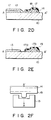
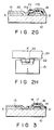
- Figs. 2A-2H illustrate steps for manufacturing a matrix array substrate according to an embodiment of the invention.
- Figs. 2A, 2B, 2D, 2E, and 2G show cross sections of the substrate plan views of which shown in Figs. 2C, 2F, and 2H, along the line A-A'.
- a transparent conductive layer 11 made of, for example, a 1,000 ⁇ -thick ITO film is formed on a transparent substrate 10 made of a 1.1mm-thick glass, with an alkali-protection film (not shown) of, for example, SiO2 provided on a surface thereof, by a spattering method.
- the temperature of the substrate is raised up to 250°C to enhance the transmissivity thereof, and sufficiently lower the resistance for a better etching processability.
- a resist photosensitive resin
- this layer 1 is exposed using a photomask.
- the layer 1 is then developed to obtain a resist pattern 12.
- the resist pattern 12 is formed on the transparent conductive layer 11 at the sections where a picture element electrode and an interconnection are to be formed, not at the section where a device is to be formed.
- etching solution water, hydrochloric acid, and nitric acid are mixed at the ratio of 1 : 1 : 0.1 (by volume) to prepare an etching solution.
- the etching solution is warmed up to 30°C, and with this solution, the transparent conductive layer 11 is etched using the resist pattern 12 as a mask.
- a picture electrode 13 and wiring layer 14 having the same pattern as the resist pattern 12 are prepared as is shown in Fig. 2C.
- the resist pattern 12 is removed.
- reference numeral 15 denotes the region where an MIM device is to be formed.
- a tantalum film 17 having the thickness of 0.3 ⁇ m is formed by a spattering method as can be seen Fig. 2D.
- this resist film is exposed using a photomask.
- the resist film is then developed to obtain a resist pattern 18.
- the Ta film 17 is etched using the resist pattern 18 as a mask. This etching is conducted in a plasma of a mixture gas of CF4 and O2 at an equivalent amount.
- the Ta film 17 is patterned, and the edge of this pattern is shaped into a taper-like slope. It has been proved that the picture element electrode 13 and wiring layer 14 which have been already made are not etched, or change their properties during this etching.
- the Ta film 17 is patterned into the first electrode 17a of the MIM element, and interconnection 17b connected thereto.
- anodic oxidation treatment is carried out in a acidic electrolytic solution (0.05 weight% citric acid solution) using the Ta films 17a and 17b as anodes.
- a acidic electrolytic solution 0.05 weight% citric acid solution
- an insulation layer 19 having an appropriate thickness are formed on the upper and side surfaces of the Ta layers 17a and 17b by controlling the voltage applied in the solution. In this embodiment, an voltage of 42 volts is applied, and the insulation layer 19 of the thickness of 700 ⁇ is thus obtained.
- the 280 ⁇ -thick Ta surface portions thereof are changed into 700 ⁇ -thick Ta2O5 surface portions.
- a Ti film 20 having the thickness of 1500 angstrom is formed on the entire surface of the product.
- a resist photosensitive resin
- this product is exposed using a photomask, and developed to obtain a resist pattern 21.
- the etching solution prepared by mixing 9g of EDTA (ethylene diamine tetra aceticazide), 400cc of water, 216cc of hydrogen peroxide solution, and 30ml of ammonia solution, is used to etch the Ti film 20 at room temperature using the resist pattern as a mask, to obtain the second electrode 22 of the MIM element, as shown in Fig. 2H.
- the resist of the surface portion is removed.
- a matrix array substrate is completed, and such a matrix array substrate has a structure in which MIM elements (non-linear resistive devices) 23 each of which has a metal-insulator-metal lamination, i.e., Ta film 17a - insulation layer 19 - Ti film 20, are arrayed on the transparent substrate 10, and a picture element electrode 13 is arranged in series to each of the non-linear resistive devices 22, and the lines of the array are connected with each other by the interconnection electrode 24 made of a laminate of the transparent conductive layer 14 and the Ta film 17b, and so are the columns thereof.
- MIM elements non-linear resistive devices
- the resistance of the product is lower than that of the conventional techniques in which layers are directly formed on a glass substrate. Since the transparent conductive layer 14 is not present at the region of the non-linear resistive device 22, that is, underneath the Ta layer 17a which is the first electrode of the non-linear resistive device 22, the MIM characteristics can be maintained at an excellent level. Further, the inter-connection electrode 24 has a double-layered structure made of the transparent conductive layer 14 and the Ta film 17b; therefore disconnection is less likely to take place than the case of an array of a Ta single layer structure.
- a orientation film made of a polyimide resin is further applied on the non-linear-resistive-device-formed surface of the matrix array substrate, followed by sintering.
- the orientation film is then rubbed to regulate the orientation of the liquid crystals.
- a common electrode made of, for example, ITO is formed on a substrate made of, for example, the same glass as used as the matrix array substrate, and at the same time, an opposed substrate in which the direction of the liquid crystal orientation is regulated by an orientation film made of polyimide resin, and rubbing, is prepared.
- the matrix array substrate and the opposed substrate are supported to have an interval of 5-20 ⁇ m therebetween so that the liquid crystals, injected therebetween, can be twisted by about 90° as regards the longitudinal direction of the molecules of the liquid crystals from the matrix array substrate to the opposed substrate.
- two polarized plate the polarization axis of each of which is twisted by about 90°.
- This embodiment has the same structure as the first one except that a metal plate layer is formed on the surface of the transparent conductive layer 14, which is one of the element of the interconnection electrode 24 besides the Ta layer 17b. Explanations of the same sections will be omitted here.
- electrolytic plating is carried out on the product having the structure shown in Fig. 2C in a plating solution prepared by mixing nickel nitride, nickel chloride, and boric acid (note that ITO film formed at a high temperature has a great resistance), thereby forming a metal thin film 16, formed of, for example, Ni on the transparent conductive layer 14, as shown in Fig. 3.
- a matrix array substrate as shown in Fig. 2H is completed, and such a matrix array substrate has a structure in which MIM elements (non-linear resistive devices) 23 each of which has a metal-insulator-metal lamination, i.e., Ta film 17a - insulation layer 19 - Ti film 20, are arrayed on the transparent substrate 10, and a picture element electrode 13 is arranged in series to each of the non-linear resistive devices 22, and the lines of the array are connected with each other by the interconnection electrode 24 made of a laminate of the transparent conductive layer 14 and the Ta film 17b, and so are the columns thereof.
- MIM elements non-linear resistive devices
- the interconnection electrode 24 includes the transparent conductive layer 14 and the metal thin film layer 15, the resistance of the interconnection electrode 24 can be made lower than that of the conventional techniques. Since the transparent conductive layer 14 and the metal thin film 15 are not present at the region of the non-linear resistive device 22, the MIM characteristics can be maintained at an excellent level. Further, the interconnection electrode 24 has a triple-layered structure made of the transparent conductive layer 14, metal thin film layer 16, and the Ta film 17b; therefore disconnection is less likely to take place than the case of an array of a Ta single layer structure.
- the present invention has realized lowering of the resistance of the interconnection electrode easily without deteriorating the characteristics of the non-linear resistive device, and is very advantageous when employed in matrix-type liquid crystal display devices of a large scale and fine images.
Abstract
Description
- The present invention relates to a matrix array substrate including a non-linear resistive device, more specifically as an MIM (Metal-Insulator-Metal) element, serving as a switching device, and a method of manufacturing the same.
- Recently, liquid crystal display devices are used in relatively simple devices such as watches, calculators, various types of measuring instruments, and even in devices handling a great amount of data such as office automation terminal devices and television sets. In the field of the liquid crystal devices, improvement of the quality of images has been of the greatest interest. Presently, there are many types of switching arrays proposed for those devices. Of all the types, one with a bi-terminal non-linear resistive device is very popular because of its simple structure and easy assembling procedure, and more specifically, an MIM type element array can be provided for its present commercial success.
- Fig. 1 is a cross section of a pixel of an array substrate having an MIM element, and the MIM element is produced as follows:
ATa film 2 is formed on a glass substrate by a thin film formation method such as spattering or vacuum deposition, or the like. Then, theTa film 2 is patterned by a photo-lithography, thereby forming a wiring and one of the two electrodes of an MIM element. After that, the surface of theTa film 2 is oxidized in an aqueous solution of citric acid by the anodic oxidation method, forming anoxide film 3. Further, aCr film 4, which serves as the other electrode, is formed by the thin film formation method, thereby completing an MIM element. Lastly, a transparentpicture element electrode 5 for image display is formed such that it is connected to the MIM element. - A basic technique of manufacturing such an array substrate is disclosed in Published Examined Japanese Patent Application (PEJPA) No. 1-35352, and a remodeled version of this technique is set forth in Published Unexamined Japanese Patent Application (PUJPA) No. 58-35352.
- In conventional MIM elements, as set forth in PEJPA No. 1-35352, the same metal is used for one of the electrodes and the wiring. Consequently, it is not always assured that a material having a small electric resistance is used. Although the β-type tantalum widely used is an excellent material for an MIM element, it has a high resistance. If the resistance of a wiring electrode is high, the waveform of a driving pulse applied from an external drive circuit is distorted. As a result, deterioration and decline of contrast occurs due to lack of writing. Especially, in the case where a display screen or display capacity is large, the width and length of the wiring become narrow and long, rendering the above problem occurred worse. Thus, in order to produce a device of a high performance, which can display a uniform image, it is essential in a practical sense that the resistance of the wiring electrode is reduced to a certain level.
- However, if different metals are used for the one of the electrodes of the MIM element, and the wiring electrode, some additional steps is required. Such addition of steps complicates the manufacturing procedure. Therefore, the reduction of the resistance must be achieved by a slightest possible modification to the conventional materials and procedure.
- It is an object of the present invention to provide a matrix array substrate in which the resistance of the wiring electrode can be lowered by using similar materials to those of the conventional technique, and without providing additional lithography steps thereto.
- It is another object of the invention to provide a method of manufacturing such a matrix array substrate.
- According to the present invention, there is provided a matrix array substrate for a liquid crystal display device, comprising a transparent substrate, a plurality of picture element electrodes formed on said transparent substrate and made of a transparent conductive material, and non-linear resistive devices formed on said transparent substrate, and each connected to each of the picture element electrodes, wherein each of said non-linear resistive devices includes a Ta first electrode formed on said transparent substrate, a second electrode, and an insulating layer located between the first and second electrodes, said first electrode being connected to another non-linear resistive device via a Ta interconnecting layer, and a transparent conductive layer is formed between said transparent substrate and interconnecting layer and is not formed between the transparent substrate and the first electrode.
- Further, according to the invention, there is also provided a method of preparing a matrix array substrate for a liquid crystal display device comprising the steps of forming a transparent conductive layer on a transparent substrate, forming a plurality of picture element electrodes and transparent conductive layers by patterning said transparent conductive interconnection layer, forming Ta first electrodes on regions of said transparent substrate where said non-linear resistive devices are to be formed, and Ta metal interconnection layers on said transparent conductive interconnection layers, forming insulating layers on said first electrodes, and forming second electrodes connected to said picture element electrodes, on said insulating layer, wherein said first electrodes, insulating layers, and second electrodes constitute the non-linear resistive devices, and are connected with each other.
- This invention can be more fully understood from the following detailed description when taken in conjunction with the accompanying drawings, in which:
- Fig. 1 is a cross sectional view showing a single picture element portion of a conventional matrix array substrate;
- Figs. 2A-2H are cross sectional views showing steps of manufacturing a matrix array substrate, according to an embodiment of the invention; and
- Fig. 3 is a cross sectional view showing one step of manufacturing a matrix array substrate procedure according to another embodiment of the invention.
- In the matrix array substrate of the present invention, one of the electrodes, i.e. the first electrode, of the non-linear resistive device (MIM element), and the interconnection layer connected to the electrode are both made of tantalum, and a transparent conductive layer, for example, ITO (indium-tin oxide) film is provided underneath this interconnection layer.
- The thickness of the Ta layer should preferably be in the range between 2000Å and 4000Å, and the thickness of the transparent conductive layer should be preferably be in the range between 500Å and 1500Å.
- The other one of the electrodes, i.e., the second electrode, of the MIM element can be any one selected from the group of Ti, Mo, Aℓ, Ag, and Cr. It should be noted here that Ta, as of the first electrode, may be used also for the second electrode. The insulation layer located between the first and second electrodes can be formed by anodic oxidation of the first electrode.
- The transparent conductive layer located underneath the interconnection layer can be prepared by patterning the transparent conductive layer formed on the entire surface of the substrate. This preparation is carried out at the same time as formation of the picture element electrode connected to the other electrode (the second electrode) of the MIM element, before the formation of the Ta layer, and is not regarded as an additional complex exposing step.
- The Ta film formed on the transparent conductive layer exhibits properties similar to those of the α type crystal system (hexagonal crystal system) having a very low resistance, and this fact was experimentally proved as will be set forth later. Thus, formation of a transparent conductive layer underneath the interconnection layer influences the interconnection layer to reduce its resistance. Consequently, display with a large capacity, and fine quality can be achieved.
- In the meantime, underneath the other electrode of the MIM electrode, no transparent conductive layer is formed; therefore the Ta film is of the β type crystal system (tetragonal crystal system). Consequently, structural change (β-Ta → α-Ta) does not occur in Ta which construct the other one of the electrodes of the non-linear resistive device. Thus, excellent MIM properties can be expected from this device.
- Further, as a display area enlarges and displayed image becomes finer, the interconnection layer inevitably becomes narrower and longer, in which case, the resistance thereof should be further decreased, according to a general technique. However, the inventors of the present invention has discovered that when a simple metal layer is formed on the ITO film by a plating method, the α type of tantalum of the layer formed thereon is further prominent, and therefore, the resistance of an interconnection layer is remarkably reduced due to not only the metal layer, but also the type of tantalum. Here, it should be noted that the plating layer formed only on the interconnection section of the ITO film, and there should be no plating layer underneath the Ta layer which constructs the other one of the electrodes of the MIM element. An MIM element, the first electrode of which is made of α type Ta, has a problem of large leak current, which causes deterioration of the switching property; therefore a pattern in which a section of the ITO film corresponding to the interconnection area is removed in advance, is first formed, the film is plated on the ITO film pattern, and then a pattern of the Ta layer is formed. With the above mentioned procedure, a matrix array substrate including an interconnection electrode of a lowered resistance, and having an MIM property equivalent to the conventional ones, can be prepared.
- The inventors of the present invention conducted experiments to analyze crystal types of the tantalum layer formed on a various kinds of substrates. The following are the results of the experiments.
-
- A: A substrate having a structure in which a Ta film having 3,000 angstrom is formed on a glass substrate by a spattering method.
- B: A substrate having a structure in which an ITO film having 3,000 angstrom is formed on a glass substrate by a spattering method, and then a Ta film having 3,000 angstrom is formed on the ITO film by a spattering method.
- C: A substrate having a structure in which an ITO film having 3,000 angstrom is formed on a glass substrate by a spattering method, an Ni film having 1,000 angstrom is formed thereon by an electrolytic plating method, and a Ta film having 3,000 angstrom is formed thereon by a spattering method.
- Crystal structure of the Ta film:
- Sample A :
- β - Ta
- Sample B :
- α - Ta (with a little bit of β - Ta mixed therein
- Sample C :
- α - Ta
- Resistivity of Ta film (influence of ITO and Ni has been subtracted by calculation)
- Sample A :
- 160-180 µΩ·cm
- Sample B :
- 50-100 µΩ·cm
- Sample C :
- 35-50 µΩ·cm
- In order to prepare a liquid crystal element of a finer image and higher quality than that of the conventional element of a 12-inch type, i.e., an element having a picture element pitch of 1/3 that of the conventional one, the resistivity of its interconnection layer need to be 60 µΩ·cm or less.
- Elements having a similar structure and size to that of an embodiment described later, can be prepared by anodic oxidation of the Ta films using the mentioned samples, and the MIM element characteristics Ioff (current flowing at 4V, the lower, the better) thereof:
- Sample A :
- to 10⁻¹³ A
- Sample B :
- to 10⁻¹⁰ A
- Sample C :
- to 10⁻¹⁰ A
- In order to prepare an element exhibiting a contrast twice as much as that of a conventional liquid crystal display element of a 12-inch type Ion/Ioff should be about 10⁵, where I on is usually 10⁻⁸.
- Further, the present invention has a structure in which a transparent conductive layer underneath the Ta interconnection layer; therefore even if some disconnection occurs within the interconnection layer, it can be recovered by the ITO film patterned for such a recovery. Further, formation of the picture element electrode and the ITO film is carried out prior to the formation of the Ta layer, and such a procedure makes formation of a film at a high temperature, and patterning thereof with a strong etchant, possible. This is another advantage of the invention in terms of process of the element.
- As the plating layer, which is an underlying layer for the Ta layer, many kinds of electrolytic plating metals of those which can be formed on the ITO film of the interconnection portion, and some of the examples are single metals such as Cu, Ni, Cr, Zn, Sn, Au, Ag, etc., or alloys such as Cu-Zn, Sn-Co, Fe-W, Co-W, Fc-Mo, Fe-Ta, Ni-P, Ni-Ta, etc. Besides these metals and alloys, laminated layers of the mentioned ones exhibit a similar effect.
- The following are explanations of preferred embodiments of the present inventions with reference to drawings.
- Figs. 2A-2H illustrate steps for manufacturing a matrix array substrate according to an embodiment of the invention. Figs. 2A, 2B, 2D, 2E, and 2G show cross sections of the substrate plan views of which shown in Figs. 2C, 2F, and 2H, along the line A-A'.
- First, as can be seen Fig. 2A, a transparent
conductive layer 11 made of, for example, a 1,000Å-thick ITO film is formed on atransparent substrate 10 made of a 1.1mm-thick glass, with an alkali-protection film (not shown) of, for example, SiO₂ provided on a surface thereof, by a spattering method. During this step, the temperature of the substrate is raised up to 250°C to enhance the transmissivity thereof, and sufficiently lower the resistance for a better etching processability. With the conventional techniques in which a picture element electrode is formed after formation of a device, the above-described step is impossible to perform appropriately because the device is damaged by heat. Therefore, in the conventional techniques, the substrate is heated only up to about 180°C to avoid a possible obstacle to stabilization of the film quality. - Next, as shown in Fig. 2B, after a resist (photosensitive resin) is applied on the entire surface of the transparent conductive layer 1, this layer 1 is exposed using a photomask. The layer 1 is then developed to obtain a resist
pattern 12. The resistpattern 12 is formed on the transparentconductive layer 11 at the sections where a picture element electrode and an interconnection are to be formed, not at the section where a device is to be formed. - Then, water, hydrochloric acid, and nitric acid are mixed at the ratio of 1 : 1 : 0.1 (by volume) to prepare an etching solution. The etching solution is warmed up to 30°C, and with this solution, the transparent
conductive layer 11 is etched using the resistpattern 12 as a mask. Thus, apicture electrode 13 andwiring layer 14 having the same pattern as the resistpattern 12 are prepared as is shown in Fig. 2C. After that, the resistpattern 12 is removed. As shown in Fig. 2C,reference numeral 15 denotes the region where an MIM device is to be formed. - Following the above, a
tantalum film 17 having the thickness of 0.3 µm is formed by a spattering method as can be seen Fig. 2D. After applying a resist on the entire surface of theTa layer 17, this resist film is exposed using a photomask. The resist film is then developed to obtain a resistpattern 18. Further, as shown in Fig. 2E, theTa film 17 is etched using the resistpattern 18 as a mask. This etching is conducted in a plasma of a mixture gas of CF₄ and O₂ at an equivalent amount. - After this etching, the
Ta film 17 is patterned, and the edge of this pattern is shaped into a taper-like slope. It has been proved that thepicture element electrode 13 andwiring layer 14 which have been already made are not etched, or change their properties during this etching. When theTa film 17 is patterned into thefirst electrode 17a of the MIM element, andinterconnection 17b connected thereto. - After removing the resist
pattern 18, anodic oxidation treatment is carried out in a acidic electrolytic solution (0.05 weight% citric acid solution) using theTa films insulation layer 19 having an appropriate thickness are formed on the upper and side surfaces of the Ta layers 17a and 17b by controlling the voltage applied in the solution. In this embodiment, an voltage of 42 volts is applied, and theinsulation layer 19 of the thickness of 700Å is thus obtained. On that surface of theTa films - Thereafter, as can be seen in Fig. 2G, a
Ti film 20 having the thickness of 1500 angstrom is formed on the entire surface of the product. After applying a resist (photosensitive resin) on the product, this product is exposed using a photomask, and developed to obtain a resistpattern 21. Then, the etching solution prepared by mixing 9g of EDTA (ethylene diamine tetra aceticazide), 400cc of water, 216cc of hydrogen peroxide solution, and 30mℓ of ammonia solution, is used to etch theTi film 20 at room temperature using the resist pattern as a mask, to obtain thesecond electrode 22 of the MIM element, as shown in Fig. 2H. Lastly, the resist of the surface portion is removed. - Thus, a matrix array substrate is completed, and such a matrix array substrate has a structure in which MIM elements (non-linear resistive devices) 23 each of which has a metal-insulator-metal lamination, i.e.,
Ta film 17a - insulation layer 19 -Ti film 20, are arrayed on thetransparent substrate 10, and apicture element electrode 13 is arranged in series to each of the non-linearresistive devices 22, and the lines of the array are connected with each other by theinterconnection electrode 24 made of a laminate of the transparentconductive layer 14 and theTa film 17b, and so are the columns thereof. - In this embodiment, since at least a part of the
Ta film 17b constituting theinterconnection electrode 24 is formed on the transparentconductive layer 14, the resistance of the product is lower than that of the conventional techniques in which layers are directly formed on a glass substrate. Since the transparentconductive layer 14 is not present at the region of the non-linearresistive device 22, that is, underneath theTa layer 17a which is the first electrode of the non-linearresistive device 22, the MIM characteristics can be maintained at an excellent level. Further, theinter-connection electrode 24 has a double-layered structure made of the transparentconductive layer 14 and theTa film 17b; therefore disconnection is less likely to take place than the case of an array of a Ta single layer structure. - Further, in order to manufacture a matrix-type liquid crystal display device from the matrix array substrate obtained as above, the following procedure may be suggested.
- First, a orientation film made of a polyimide resin is further applied on the non-linear-resistive-device-formed surface of the matrix array substrate, followed by sintering. The orientation film is then rubbed to regulate the orientation of the liquid crystals. In the meantime, a common electrode made of, for example, ITO, is formed on a substrate made of, for example, the same glass as used as the matrix array substrate, and at the same time, an opposed substrate in which the direction of the liquid crystal orientation is regulated by an orientation film made of polyimide resin, and rubbing, is prepared. Then, the matrix array substrate and the opposed substrate are supported to have an interval of 5-20 µm therebetween so that the liquid crystals, injected therebetween, can be twisted by about 90° as regards the longitudinal direction of the molecules of the liquid crystals from the matrix array substrate to the opposed substrate. Outside thus structured liquid crystal cell, there are provided two polarized plate the polarization axis of each of which is twisted by about 90°.
- The following is an explanation of another preferred embodiment according to the present invention.
- This embodiment has the same structure as the first one except that a metal plate layer is formed on the surface of the transparent
conductive layer 14, which is one of the element of theinterconnection electrode 24 besides theTa layer 17b. Explanations of the same sections will be omitted here. - In this embodiment, electrolytic plating is carried out on the product having the structure shown in Fig. 2C in a plating solution prepared by mixing nickel nitride, nickel chloride, and boric acid (note that ITO film formed at a high temperature has a great resistance), thereby forming a metal
thin film 16, formed of, for example, Ni on the transparentconductive layer 14, as shown in Fig. 3. - Thus, a matrix array substrate as shown in Fig. 2H is completed, and such a matrix array substrate has a structure in which MIM elements (non-linear resistive devices) 23 each of which has a metal-insulator-metal lamination, i.e.,
Ta film 17a - insulation layer 19 -Ti film 20, are arrayed on thetransparent substrate 10, and apicture element electrode 13 is arranged in series to each of the non-linearresistive devices 22, and the lines of the array are connected with each other by theinterconnection electrode 24 made of a laminate of the transparentconductive layer 14 and theTa film 17b, and so are the columns thereof. - In this embodiment, at least a part of the
interconnection electrode 24 includes the transparentconductive layer 14 and the metalthin film layer 15, the resistance of theinterconnection electrode 24 can be made lower than that of the conventional techniques. Since the transparentconductive layer 14 and the metalthin film 15 are not present at the region of the non-linearresistive device 22, the MIM characteristics can be maintained at an excellent level. Further, theinterconnection electrode 24 has a triple-layered structure made of the transparentconductive layer 14, metalthin film layer 16, and theTa film 17b; therefore disconnection is less likely to take place than the case of an array of a Ta single layer structure. - The present invention has realized lowering of the resistance of the interconnection electrode easily without deteriorating the characteristics of the non-linear resistive device, and is very advantageous when employed in matrix-type liquid crystal display devices of a large scale and fine images.
Claims (13)
- A matrix array substrate for a liquid crystal display device comprising:
a transparent substrate (10);
a plurality of picture element electrodes (13) formed on said transparent substrate (10) and made of a transparent conductive material; and
non-linear resistive devices formed on said transparent substrate (10), and each connected to each of the picture element electrodes (13);
wherein each of said non-linear resistive devices includes a Ta first electrode (17a) formed on said transparent substrate (10), a second electrode (20), and an insulating layer (19) located between the first and second electrodes (17a, 20), said first electrode (17a) being connected to another non-linear resistive device via a Ta interconnecting layer (17b), and a transparent conductive layer (14) is formed between said transparent substrate (10) and Ta interconnecting layer (17b) and is not formed between the transparent substrate (10) and the first electrode. - A matrix array substrate according to claim 1, characterized in that said second electrode (20) is a metal selected from the group consisting of Ti, Mo, Aℓ, Ag, Cr and Ta.
- A matrix array substrate according to claim 1, characterized in that said insulating layer (19) is tantalum oxide formed by anodic oxidation of the first electrode.
- A matrix array substrate according to claim 1, characterized in that said transparent conductive material is indium-tin oxide.
- A matrix array substrate according to claim 1, characterized in that a metal layer (16) is formed on the transparent conductive layer (14).
- A matrix array substrate according to claim 1, characterized in that said metal layer (16) is a metal selected from the group consisting of Cu, Ni, Cr, Zn, Sn, Au, Ag, Cu-Zn alloy, Sn-Co alloy, Fe-W alloy, Co-W alloy, Fe-Mo alloy, Fe-Ta alloy, Ni-P alloy, Ni-Ta alloy and a laminated body thereof.
- A method of preparing a matrix array substrate for a liquid crystal display device comprising the steps of:
forming a transparent conductive layer (11) on a transparent substrate (10);
forming a plurality of picture element electrodes (13) and transparent conductive interconnection layers (14) by patterning said transparent conductive layer (11);
forming Ta first electrodes (17a) on regions of said transparent substrate (10) where said non-linear resistive devices are to be formed, and Ta metal interconnection layers (17b) on said transparent conductive interconnection layers (14);
forming insulating layers (19) on said first electrodes (17a); and
forming second electrodes (20) connected to said picture element electrodes (13), on said insulating layer (19);
wherein said first electrodes (17a), insulating layers (19), and second electrodes (20) constitute the non-linear resistive devices, and the non-linear resistive devices are connected with each other. - A method of preparing a matrix array substrate according to claim 7, characterized in that said step of forming said first electrodes (17a) and metal interconnection layers (17b) is carried out by patterning a Ta layer (11) after Ta is applied on an entire surface thereof.
- A method of preparing a matrix array substrate according to claim 7, characterized in that said step of forming insulating layers (19) on said first electrodes (17a) is carried out through anodic oxidation of surfaces of said first electrodes (17a) and Ta interconnection layer (17b).
- A method of preparing a matrix array substrate according to claim 7, characterized in that said second electrode (20) is a metal selected from the group of Ti, Mo, Aℓ, Ag, Cr, and Ta.
- A method of preparing a matrix array substrate according to claim 7, characterized in that said transparent conductive layer (11) is formed of indium-tin oxide.
- A method of preparing a matrix array substrate according to claim 7, characterized by further comprising the step of forming metal layer (16) on surface of said transparent conductive interconnection layer (14).
- A method of preparing a matrix array substrate according to claim 7, characterized in that said step of forming said metal layer (16) is carried out by plating said transparent conductive interconnection layer with a metal selected from the group consisting of Cu, Ni, Cr, Zn, Sn, Au, Ag, Cu-Zn alloy, Sn-Co alloy, Fe-W alloy, Co-W alloy, Fe-Mo alloy, Fe-Ta alloy, Ni-P alloy, Ni-Ta alloy and a laminated body thereof.
Applications Claiming Priority (4)
| Application Number | Priority Date | Filing Date | Title |
|---|---|---|---|
| JP31436790A JP2585465B2 (en) | 1990-11-21 | 1990-11-21 | Matrix array substrate |
| JP314367/90 | 1990-11-21 | ||
| JP119973/91 | 1991-05-24 | ||
| JP3119973A JPH04346319A (en) | 1991-05-24 | 1991-05-24 | Matrix array substrate and manufacture thereof |
Publications (2)
| Publication Number | Publication Date |
|---|---|
| EP0487055A1 true EP0487055A1 (en) | 1992-05-27 |
| EP0487055B1 EP0487055B1 (en) | 1996-05-22 |
Family
ID=26457620
Family Applications (1)
| Application Number | Title | Priority Date | Filing Date |
|---|---|---|---|
| EP91119766A Expired - Lifetime EP0487055B1 (en) | 1990-11-21 | 1991-11-19 | Matrix array substrate |
Country Status (5)
| Country | Link |
|---|---|
| US (1) | US5274482A (en) |
| EP (1) | EP0487055B1 (en) |
| KR (1) | KR950002288B1 (en) |
| DE (1) | DE69119709T2 (en) |
| TW (1) | TW201343B (en) |
Cited By (1)
| Publication number | Priority date | Publication date | Assignee | Title |
|---|---|---|---|---|
| EP1587139A2 (en) * | 2004-04-15 | 2005-10-19 | Hewlett-Packard Development Company, L.P. | Method of making a tantalum layer and apparatus using a tantalum layer |
Families Citing this family (6)
| Publication number | Priority date | Publication date | Assignee | Title |
|---|---|---|---|---|
| JP2915732B2 (en) * | 1993-02-01 | 1999-07-05 | シャープ株式会社 | Active matrix substrate |
| JPH06310492A (en) * | 1993-04-23 | 1994-11-04 | Fuji Xerox Co Ltd | Etchant for titanium thin film and manufacture semiconductor device |
| WO1996014599A1 (en) * | 1994-11-08 | 1996-05-17 | Citizen Watch Co., Ltd. | Liquid crystal display |
| US6086777A (en) * | 1998-07-02 | 2000-07-11 | Advanced Micro Devices, Inc. | Tantalum barrier metal removal by using CF4 /o2 plasma dry etch |
| JP2001075501A (en) * | 1999-07-02 | 2001-03-23 | Seiko Instruments Inc | Display device and method for inspection of display device |
| JP3376969B2 (en) * | 1999-09-02 | 2003-02-17 | 株式会社村田製作所 | Surface acoustic wave device and method of manufacturing the same |
Citations (1)
| Publication number | Priority date | Publication date | Assignee | Title |
|---|---|---|---|---|
| US5000545A (en) * | 1987-05-28 | 1991-03-19 | Canon Kabushiki Kaisha | Liquid crystal device with metal electrode partially overlying transparent electrode |
Family Cites Families (8)
| Publication number | Priority date | Publication date | Assignee | Title |
|---|---|---|---|---|
| JPS57205712A (en) * | 1981-06-12 | 1982-12-16 | Seiko Epson Corp | Production of liquid crystal display body |
| JPS5838923A (en) * | 1981-09-01 | 1983-03-07 | Seiko Epson Corp | Manufacture of liquid crystal display substrate |
| JPS6420539A (en) * | 1987-07-15 | 1989-01-24 | Konishiroku Photo Ind | Silver halide photographic sensitive material with improved writing and erasing properties |
| US4859036A (en) * | 1987-05-15 | 1989-08-22 | Canon Kabushiki Kaisha | Device plate having conductive films selected to prevent pin-holes |
| JPH0666016B2 (en) * | 1987-05-28 | 1994-08-24 | キヤノン株式会社 | Liquid crystal element |
| JP2746403B2 (en) * | 1989-02-13 | 1998-05-06 | コニカ株式会社 | Liquid crystal display device and manufacturing method thereof |
| US5128784A (en) * | 1989-03-23 | 1992-07-07 | Seiko Epson Corporation | Active matrix liquid crystal display device and method for production thereof |
| JP2795883B2 (en) * | 1989-03-24 | 1998-09-10 | シチズン時計株式会社 | Nonlinear element in liquid crystal display |
-
1991
- 1991-11-15 TW TW080108990A patent/TW201343B/zh active
- 1991-11-19 DE DE69119709T patent/DE69119709T2/en not_active Expired - Fee Related
- 1991-11-19 EP EP91119766A patent/EP0487055B1/en not_active Expired - Lifetime
- 1991-11-21 KR KR1019910020889A patent/KR950002288B1/en not_active IP Right Cessation
- 1991-11-21 US US07/796,248 patent/US5274482A/en not_active Expired - Fee Related
Patent Citations (1)
| Publication number | Priority date | Publication date | Assignee | Title |
|---|---|---|---|---|
| US5000545A (en) * | 1987-05-28 | 1991-03-19 | Canon Kabushiki Kaisha | Liquid crystal device with metal electrode partially overlying transparent electrode |
Non-Patent Citations (4)
| Title |
|---|
| MOLECULAR CRYSTALS AND LIQUID CRYSTALS. vol. 193, December 1990, CHUR, CH pages 1 - 5; A.SMIRNOV ET AL.: 'High multiplexed MIM-addressed LCD' * |
| PATENT ABSTRACTS OF JAPAN vol. 14, no. 581 (P-114)26 December 1990 * |
| PATENT ABSTRACTS OF JAPAN vol. 7, no. 121 (P-199)25 May 1983 & JP-A-58 038 923 ( SUWA SEIKOSHA ) 7 March 1983 * |
| PATENT ABSTRACTS OF JAPAN vol. 7, no. 60 (P-182)12 March 1983 & JP-A-57 205 712 ( SUWA SEIKOSHA ) 16 December 1982 * |
Cited By (3)
| Publication number | Priority date | Publication date | Assignee | Title |
|---|---|---|---|---|
| EP1587139A2 (en) * | 2004-04-15 | 2005-10-19 | Hewlett-Packard Development Company, L.P. | Method of making a tantalum layer and apparatus using a tantalum layer |
| EP1587139A3 (en) * | 2004-04-15 | 2006-05-24 | Hewlett-Packard Development Company, L.P. | Method of making a tantalum layer and apparatus using a tantalum layer |
| US7445810B2 (en) | 2004-04-15 | 2008-11-04 | Hewlett-Packard Development Company, L.P. | Method of making a tantalum layer and apparatus using a tantalum layer |
Also Published As
| Publication number | Publication date |
|---|---|
| KR950002288B1 (en) | 1995-03-16 |
| DE69119709D1 (en) | 1996-06-27 |
| TW201343B (en) | 1993-03-01 |
| EP0487055B1 (en) | 1996-05-22 |
| DE69119709T2 (en) | 1996-10-31 |
| US5274482A (en) | 1993-12-28 |
Similar Documents
| Publication | Publication Date | Title |
|---|---|---|
| EP0898785B1 (en) | Active matrix displays and method of making | |
| US4543573A (en) | Display panel | |
| US5485294A (en) | Process for producing MIM elements by electrolytic polymerization | |
| EP0506117A2 (en) | Thin-film transistor | |
| EP0487055B1 (en) | Matrix array substrate | |
| US5539549A (en) | Active matrix substrate having island electrodes for making ohmic contacts with MIM electrodes and pixel electrodes | |
| JP2778746B2 (en) | Liquid crystal display device and method of manufacturing electrode substrate | |
| JPH06160877A (en) | Thin-film wiring structure and liquid crystal display device formed by using the structure | |
| JPH04346319A (en) | Matrix array substrate and manufacture thereof | |
| JP3384022B2 (en) | Liquid crystal device and nonlinear resistance element | |
| JPH052191A (en) | Production of matrix substrate | |
| KR100278695B1 (en) | Liquid crystal display element and method of fabricating electrode substrate for use in the liquid crystal display element | |
| JPH07168208A (en) | Active matrix system liquid crystal display | |
| JP2845929B2 (en) | Manufacturing method of nonlinear element | |
| JPH0511277A (en) | Production of matrix array substrate | |
| JP3196986B2 (en) | Manufacturing method of array substrate | |
| JPH052192A (en) | Matrix array substrate and production thereof | |
| JPH04253033A (en) | Liquid crystal display device | |
| JPH06160911A (en) | Liquid crystal display device | |
| JPH06324355A (en) | Liquid crystal display panel and its production | |
| JP3341346B2 (en) | Manufacturing method of nonlinear element | |
| JPS5840527A (en) | Production of substrate for liquid crystal panel | |
| JPH06337440A (en) | Mim type nonlinear element and manufacture thereof | |
| JPH05203996A (en) | Production of matrix array substrate | |
| JPH05297415A (en) | Liquid crystal display device and its production |
Legal Events
| Date | Code | Title | Description |
|---|---|---|---|
| PUAI | Public reference made under article 153(3) epc to a published international application that has entered the european phase |
Free format text: ORIGINAL CODE: 0009012 |
|
| 17P | Request for examination filed |
Effective date: 19911216 |
|
| AK | Designated contracting states |
Kind code of ref document: A1 Designated state(s): DE FR GB |
|
| 17Q | First examination report despatched |
Effective date: 19940725 |
|
| GRAH | Despatch of communication of intention to grant a patent |
Free format text: ORIGINAL CODE: EPIDOS IGRA |
|
| GRAA | (expected) grant |
Free format text: ORIGINAL CODE: 0009210 |
|
| AK | Designated contracting states |
Kind code of ref document: B1 Designated state(s): DE FR GB |
|
| REF | Corresponds to: |
Ref document number: 69119709 Country of ref document: DE Date of ref document: 19960627 |
|
| ET | Fr: translation filed | ||
| PLBE | No opposition filed within time limit |
Free format text: ORIGINAL CODE: 0009261 |
|
| STAA | Information on the status of an ep patent application or granted ep patent |
Free format text: STATUS: NO OPPOSITION FILED WITHIN TIME LIMIT |
|
| 26N | No opposition filed | ||
| REG | Reference to a national code |
Ref country code: GB Ref legal event code: 746 Effective date: 19980917 |
|
| REG | Reference to a national code |
Ref country code: FR Ref legal event code: D6 |
|
| PGFP | Annual fee paid to national office [announced via postgrant information from national office to epo] |
Ref country code: FR Payment date: 19991109 Year of fee payment: 9 |
|
| PGFP | Annual fee paid to national office [announced via postgrant information from national office to epo] |
Ref country code: GB Payment date: 19991117 Year of fee payment: 9 |
|
| PGFP | Annual fee paid to national office [announced via postgrant information from national office to epo] |
Ref country code: DE Payment date: 19991119 Year of fee payment: 9 |
|
| PG25 | Lapsed in a contracting state [announced via postgrant information from national office to epo] |
Ref country code: GB Free format text: LAPSE BECAUSE OF NON-PAYMENT OF DUE FEES Effective date: 20001119 |
|
| GBPC | Gb: european patent ceased through non-payment of renewal fee |
Effective date: 20001119 |
|
| PG25 | Lapsed in a contracting state [announced via postgrant information from national office to epo] |
Ref country code: FR Free format text: LAPSE BECAUSE OF NON-PAYMENT OF DUE FEES Effective date: 20010731 |
|
| PG25 | Lapsed in a contracting state [announced via postgrant information from national office to epo] |
Ref country code: DE Free format text: LAPSE BECAUSE OF NON-PAYMENT OF DUE FEES Effective date: 20010801 |
|
| REG | Reference to a national code |
Ref country code: FR Ref legal event code: ST |