EP0479500A2 - Connector assembly with a series of electrical contacts - Google Patents
Connector assembly with a series of electrical contacts Download PDFInfo
- Publication number
- EP0479500A2 EP0479500A2 EP91308846A EP91308846A EP0479500A2 EP 0479500 A2 EP0479500 A2 EP 0479500A2 EP 91308846 A EP91308846 A EP 91308846A EP 91308846 A EP91308846 A EP 91308846A EP 0479500 A2 EP0479500 A2 EP 0479500A2
- Authority
- EP
- European Patent Office
- Prior art keywords
- contacts
- lead frame
- connector assembly
- ground
- housing block
- Prior art date
- Legal status (The legal status is an assumption and is not a legal conclusion. Google has not performed a legal analysis and makes no representation as to the accuracy of the status listed.)
- Granted
Links
Images


Classifications
-
- H—ELECTRICITY
- H01—ELECTRIC ELEMENTS
- H01R—ELECTRICALLY-CONDUCTIVE CONNECTIONS; STRUCTURAL ASSOCIATIONS OF A PLURALITY OF MUTUALLY-INSULATED ELECTRICAL CONNECTING ELEMENTS; COUPLING DEVICES; CURRENT COLLECTORS
- H01R13/00—Details of coupling devices of the kinds covered by groups H01R12/70 or H01R24/00 - H01R33/00
- H01R13/02—Contact members
- H01R13/04—Pins or blades for co-operation with sockets
-
- H—ELECTRICITY
- H01—ELECTRIC ELEMENTS
- H01R—ELECTRICALLY-CONDUCTIVE CONNECTIONS; STRUCTURAL ASSOCIATIONS OF A PLURALITY OF MUTUALLY-INSULATED ELECTRICAL CONNECTING ELEMENTS; COUPLING DEVICES; CURRENT COLLECTORS
- H01R13/00—Details of coupling devices of the kinds covered by groups H01R12/70 or H01R24/00 - H01R33/00
- H01R13/46—Bases; Cases
- H01R13/514—Bases; Cases composed as a modular blocks or assembly, i.e. composed of co-operating parts provided with contact members or holding contact members between them
-
- H—ELECTRICITY
- H01—ELECTRIC ELEMENTS
- H01R—ELECTRICALLY-CONDUCTIVE CONNECTIONS; STRUCTURAL ASSOCIATIONS OF A PLURALITY OF MUTUALLY-INSULATED ELECTRICAL CONNECTING ELEMENTS; COUPLING DEVICES; CURRENT COLLECTORS
- H01R12/00—Structural associations of a plurality of mutually-insulated electrical connecting elements, specially adapted for printed circuits, e.g. printed circuit boards [PCB], flat or ribbon cables, or like generally planar structures, e.g. terminal strips, terminal blocks; Coupling devices specially adapted for printed circuits, flat or ribbon cables, or like generally planar structures; Terminals specially adapted for contact with, or insertion into, printed circuits, flat or ribbon cables, or like generally planar structures
- H01R12/70—Coupling devices
- H01R12/77—Coupling devices for flexible printed circuits, flat or ribbon cables or like structures
- H01R12/771—Details
- H01R12/775—Ground or shield arrangements
-
- H—ELECTRICITY
- H01—ELECTRIC ELEMENTS
- H01R—ELECTRICALLY-CONDUCTIVE CONNECTIONS; STRUCTURAL ASSOCIATIONS OF A PLURALITY OF MUTUALLY-INSULATED ELECTRICAL CONNECTING ELEMENTS; COUPLING DEVICES; CURRENT COLLECTORS
- H01R13/00—Details of coupling devices of the kinds covered by groups H01R12/70 or H01R24/00 - H01R33/00
- H01R13/648—Protective earth or shield arrangements on coupling devices, e.g. anti-static shielding
-
- H—ELECTRICITY
- H01—ELECTRIC ELEMENTS
- H01R—ELECTRICALLY-CONDUCTIVE CONNECTIONS; STRUCTURAL ASSOCIATIONS OF A PLURALITY OF MUTUALLY-INSULATED ELECTRICAL CONNECTING ELEMENTS; COUPLING DEVICES; CURRENT COLLECTORS
- H01R12/00—Structural associations of a plurality of mutually-insulated electrical connecting elements, specially adapted for printed circuits, e.g. printed circuit boards [PCB], flat or ribbon cables, or like generally planar structures, e.g. terminal strips, terminal blocks; Coupling devices specially adapted for printed circuits, flat or ribbon cables, or like generally planar structures; Terminals specially adapted for contact with, or insertion into, printed circuits, flat or ribbon cables, or like generally planar structures
- H01R12/70—Coupling devices
- H01R12/77—Coupling devices for flexible printed circuits, flat or ribbon cables or like structures
- H01R12/778—Coupling parts carrying sockets, clips or analogous counter-contacts
-
- H—ELECTRICITY
- H01—ELECTRIC ELEMENTS
- H01R—ELECTRICALLY-CONDUCTIVE CONNECTIONS; STRUCTURAL ASSOCIATIONS OF A PLURALITY OF MUTUALLY-INSULATED ELECTRICAL CONNECTING ELEMENTS; COUPLING DEVICES; CURRENT COLLECTORS
- H01R13/00—Details of coupling devices of the kinds covered by groups H01R12/70 or H01R24/00 - H01R33/00
- H01R13/648—Protective earth or shield arrangements on coupling devices, e.g. anti-static shielding
- H01R13/658—High frequency shielding arrangements, e.g. against EMI [Electro-Magnetic Interference] or EMP [Electro-Magnetic Pulse]
- H01R13/6581—Shield structure
- H01R13/6585—Shielding material individually surrounding or interposed between mutually spaced contacts
-
- H—ELECTRICITY
- H01—ELECTRIC ELEMENTS
- H01R—ELECTRICALLY-CONDUCTIVE CONNECTIONS; STRUCTURAL ASSOCIATIONS OF A PLURALITY OF MUTUALLY-INSULATED ELECTRICAL CONNECTING ELEMENTS; COUPLING DEVICES; CURRENT COLLECTORS
- H01R13/00—Details of coupling devices of the kinds covered by groups H01R12/70 or H01R24/00 - H01R33/00
- H01R13/648—Protective earth or shield arrangements on coupling devices, e.g. anti-static shielding
- H01R13/658—High frequency shielding arrangements, e.g. against EMI [Electro-Magnetic Interference] or EMP [Electro-Magnetic Pulse]
- H01R13/6591—Specific features or arrangements of connection of shield to conductive members
- H01R13/6597—Specific features or arrangements of connection of shield to conductive members the conductive member being a contact of the connector
Definitions
- the invention relates to a connector assembly for connection to conductive wires to form a cable assembly.
- a connector assembly disclosed in U.S. Patent 4,875,877 comprises, a conductive ground bus, for connection to ground wires of at least one electrical cable, and conductive signal contacts for connection to signal wires of at least one electrical cable, the signal contacts being joined to the ground bus, an insulative housing block applied over the contacts, at least a selected one of the contacts being detached from the ground bus, and at least one of the signal contacts remaining joined to the ground bus.
- the connector assembly is constructed for ease of manufacture. For example, the contacts and the ground bus are joined together in a lead frame to eliminate separate parts.
- the housing block advantageously holds the contacts in desired positions when the contacts are connected to the wires.
- the contacts are held on pitch spacings that correspond to the pitch spacings of contact receiving cavities of an insulative housing.
- the contacts are assembled into the cavities of the housing as a group, rather than as individual contacts.
- the contacts on the lead frame being fabricated of thin metal, are easily deflected to misaligned positions.
- a housing can be applied over the contacts by injection molding fluent plastic material over portions of the contacts. The solidified plastic material is relied on to hold the contacts in their positions. If the contacts are misaligned while the housing is applied, the contacts will be held by the housing in misaligned positions.
- the invention results from a need to guide the contacts during insertion into corresponding cavities of an insulative housing.
- the contacts are formed with tapered fins.
- the fins are used for guiding the contacts into precisely oriented positions within cavities of an insulative housing.
- the fins enter slits in the housing.
- the slits urge the fins in guided progressive movement within the housing.
- the fins urge the contacts to positions that are precisely aligned within corresponding cavities of the housing.
- the cooperation between the fins and the slits will move misaligned contacts into desired positions, and thereafter will hold and retain the contacts in those positions. Assembly of the contacts into the housing is accomplished without forcible insertion of the contacts, thereby averting damage to the contacts.
- At least one electrical cable 1 is constructed with an elongated signal wire 2 or center conductor concentrically encircled by a dielectric 3, in turn encircled by a flexible insulative outer jacket 4 or sheath.
- a corresponding, elongated and conductive ground wire 5 or drain wire extends along the exterior of the dielectric 3 and is within the jacket 4.
- the cable may include a single ground wire 5, as shown, or may include first and second ground wires 5 to provide a combination of a signal wire 2 between two ground wires 5.
- the invention applies to either cable construction, or to any other cable construction, not shown.
- the cable construction is cut to expose and to project the signal wire 2, the dielectric 3 and the corresponding ground wire 5 from the jacket 4.
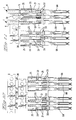
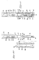
- an electrical connector assembly 6 is to be connected to one or multiple cables 1 in a manner described below. Construction of the connector assembly 6 begins with a row of electrical contacts 9. With reference to Figures 1 and 2, the contacts 9 project forwardly from a corresponding, elongated ground bus 10. A series of pilot holes 11 extend through the ground bus 10. The contacts 9 when joined to the ground bus 10 provide a lead frame, correspondingly numbered 12 or 12A, shown in Figure 2, known as an array of conductive paths for conducting electricity, with the paths joined together and cut out from a strip of metal. Each of the contacts 9 includes a pair of spaced apart fingers 13 defining an electrical receptacle 14 at a front end. The fingers 13 are cut out from the strip of metal while the metal is in a flat plane.
- each of the contacts 9 are formed by bending, such that the fingers 13 are pivoted out of the plane of the metal to oppose each other and to define therebetween the receptacle 14.
- the contacts 9 are on pitch spacings, that are the repeated spacings between longitudinal axes of the multiple contacts 9 in a row.
- the fingers 13 are cut out of portions of the metal strip that bridge between adjacent contacts 9.
- two lead frames 12, 12A with attached contacts 9 can be stacked and superimposed, laid one on the other, to provide a series of contacts 9 in a row.
- the pitch spacing of the series of contacts 9 in the row is desirably decreased to attain a compact size, when two lead frames 12A, 12B are superimposed.
- a construction is depicted wherein one of the contacts 9 is depicted in phantom outline to indicate that the contact 9 can be removed from the corresponding lead frame 12A and eliminated from the series of contacts 9.
- the contacts 9 of the lead frame 12A alternate with the contacts 9 of the second lead frame 12B in an alternating series of said contacts 9.
- Figure 13 shows a series of contacts 9 wherein no contact 9 is eliminated from the series of contacts 9.
- an insulative housing block 16 is applied to each contact 9 that remains joined to a corresponding frame 12A, 12B.
- the housing block 16 is formed by injection molding a fluent plastics material that embeds the contacts 9.
- a front end 17 of the housing block is formed with a front wall 18 extending transverse to the row of contacts.
- the housing block 16 extends to a rear wall 20 from which each ground bus 10 projects.
- Wire connecting portions 21 of the contacts 9 appear at corresponding spaced apart, openings 22 formed by molding the housing block 16.
- the housing block 16 holds all the contacts 9 on a desired pitch spacing.
- the contacts 9 are on the first and second lead frames 12A, 12B, and comprise a series of contacts 9 in a row wherein the contacts 9 of the first lead frame 12A, 12B, and the contacts 9 of the second lead frame 12A, 12B, are in the row.
- Wire receiving channels 25, formed by molding the housing block 16, extend from the rear wall 20 and forwardly and axially of corresponding contacts 9.
- the signal wire 2 of the cable 1 and each corresponding ground wire 5 of the cable 1 extend along corresponding channels 25.
- the signal wire 2 extends along the channel 25 to the wire connecting portion 21 of a corresponding contact 9.
- Each corresponding ground wire 5 extends along a corresponding channel 25 to the wire connecting portion 21 of a corresponding contact 9.
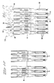
- each contact 9 that is connected to a signal wire 2 is designated a signal contact 9A.
- Each contact 9 that is connected to a ground wire is designated a ground contact 9B.
- Each contact 9 is joined to a corresponding lead frame 12A, 12B by a removable portion 38 in the form of a narrow portion of the lead frame 12A, 12B.
- an advantage of the invention resides in all the signal contacts 9A being removably joined to one lead frame 12A by the corresponding removable portions 38.
- the advantage becomes more evident with reference to Figures 10 and 11, which depict the signal contacts 9A as being separated from the remainder of the lead frame 12A, and from one another, for example, by severing and removing the removable portions 38 and the ground bus 10 from the signal contacts 9. The remainder of the lead frame 12A is discarded when no longer needed.
- another advantage of the invention is that the lead frames 12, 12A are bent, as shown at 7, to bring the contacts 9 of both lead frames 12, 12A into a common plane.
- a common plane for the contacts 9 contributes to the object of achieving precise location of the contacts 9, especially important for locating the contacts precisely, and especially important to prevent damage to the contacts 9 when they are connected to corresponding wires 2 and 5 and when they are inserted into an insulative housing 39.
- precise alignment of the contacts 9 is achieved further in the following manner.
- the removable portions 38 are attached and extend between the contacts 9 and the corresponding ground busses 10.
- the removable portions 38 are bent along their lengths to bring their forward ends into a common plane. Thereby, the bent removable portions 38 orient the contacts 9 of both lead frames 12, 12A in coplanar relationship.
- the coplanar contacts 9 are held in precise alignment when the insulative material of the housing block 16 is applied.
- the insulative material is applied by an injection molding process, with molding dies 8, 15 of a conventional, injection molding apparatus 19 holding the contacts 9 along a parting line 23 of the dies 8, 15 while the insulative material is injected into die cavities 24, 26 to form the housing block 16.
- the metal thickness of the contacts 9 is clamped between the dies 8, 15 and is held stationary. The metal thickness, where clamped, blocks the flow of fluent insulative material.
- the insulative material is blocked from covering over the wire connecting portions 21 of the contacts 9 and those portions of the contacts 9 that project from the front end 14 and from the rear wall 20 of the housing block 16.
- the solidified housing block 16 holds the contacts 9 in desired positions, including desired pitch spacings, after ejection from the dies 8, 15.
- the row of contacts 9 in Figures 10 and 11 are arranged in a series of contacts 9 wherein each of the contacts 9 of the first lead frame 12 alternates in the series with a contact 9 of the second lead frame 12. Upon removal of the first lead frame 12, the corresponding contacts 9 will be separate from one another and are designated signal contacts 9A.
- the contacts 9 of the second lead frame 12B are designated ground contacts 9 connected to the ground bus 10 of the second lead frame 12B.
- the series of contacts 9 is arranged in a desired pattern of a signal alternating with a ground or reference. The pattern can be repeated along the series. The pattern is useful in a construction wherein the pitch spacings are close together, and each signal contact 9A is required to be adjacent to at least one ground contact 9B connected to a reference potential.
- each ground contact 9B tends to shield a corresponding signal contact 9A from electrical influences that would induce an undesired voltage in the signal contact 9A.
- a construction is shown in Figure 11 wherein two ground wires 5 of two different cables 1 are connected to the same ground contact 9. Other constructions are permitted, for example, with one ground wire 5 connected to one ground contact 9.
- first ground bus 10 and the second ground bus 10 are connected, for example, by a welding operation or a soldering operation.
- At least one contact 9 of the first lead frame 12A remains joined to the ground bus 10 of the first lead frame 12A and thereby becomes a ground contact 9B.
- Figure 13 discloses a construction wherein selected contacts 9A are removed from a respective lead frame 12A, 12B and both lead frames 12A, 12B provide a conductive ground bus 10 connected to respective contacts 9B remaining joined to the lead frames 12A, 12B.
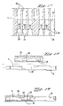
- the contacts 9 have corresponding fins 27 which project in the plane of the metal thickness laterally of the longitudinal axes of the contacts 9.
- the fins 27 of the contacts 9 of both the first lead frame 12 and second lead frame 12B are urged into a common plane prior to applying the insulative housing block 16, and prior to retaining the fins 27 in the common plane by the housing block 16.
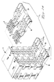
- the contacts 9 project forward of the housing block 16 for assembly with an insulative housing 39.
- the housing 39 includes multiple contact receiving cavities 40 spaced apart on pitch spacings corresponding to that of the series of contacts 9.
- a group of contacts 9 is shown fully assembled in corresponding cavities 40 in a representative row, Figure 14, with the front end 17 of the housing block 10 engaging a rear 41 of the housing 39.
- the cables 1 that are connected to the contacts 9 are omitted from Figure 14.
- the fins 27 are inserted along corresponding slits 29 in the housing 39 to guide the contacts 9 into alignment along corresponding cavities 40.
- the front edges 30 of the fins 27 are tapered to reduce frictional resistance to insertion of the tapered surfaces 30 along corresponding slits 29.
- Each of the fins 27 includes a laterally projecting barb 31 that extends diagonally rearward and penetrates the housing 39, Figure 21, to resist withdrawal of the contacts 9 in a rearward direction.
- the barbs 31 are dimensioned laterally with an interference fit with the sides of the corresponding slits 29.
- the barbs 31 are rearward of the fingers 13, which allows the contacts 9 to be inserted along the cavities 40 before the barbs 31 engage the sides of the slits 29.
- Each fin 27 is stepped laterally wider to provide a forward facing shoulder 32 that faces a rear facing shoulder 34 at a stepped wider portion of each slit 29.
- the front end 17 of the housing block 16 engages the housing 39.
- the fins 27 in the slits 29 hold flat sides 36, Figures 18 and 19, of the corresponding contacts 9 against flat side walls 35 of the cavities 40, and resist rotation of the contacts 9 in corresponding cavities 40.
- the contacts 9 are held in precise locations within corresponding cavities 40.
Abstract
Description
- The invention relates to a connector assembly for connection to conductive wires to form a cable assembly.
- A connector assembly disclosed in U.S. Patent 4,875,877 comprises, a conductive ground bus, for connection to ground wires of at least one electrical cable, and conductive signal contacts for connection to signal wires of at least one electrical cable, the signal contacts being joined to the ground bus, an insulative housing block applied over the contacts, at least a selected one of the contacts being detached from the ground bus, and at least one of the signal contacts remaining joined to the ground bus. The connector assembly is constructed for ease of manufacture. For example, the contacts and the ground bus are joined together in a lead frame to eliminate separate parts. The housing block advantageously holds the contacts in desired positions when the contacts are connected to the wires. The contacts are held on pitch spacings that correspond to the pitch spacings of contact receiving cavities of an insulative housing. The contacts are assembled into the cavities of the housing as a group, rather than as individual contacts.
- The contacts on the lead frame, being fabricated of thin metal, are easily deflected to misaligned positions. A concern exists that, the contacts will be held by a housing block in these misaligned positions. For example, a housing can be applied over the contacts by injection molding fluent plastic material over portions of the contacts. The solidified plastic material is relied on to hold the contacts in their positions. If the contacts are misaligned while the housing is applied, the contacts will be held by the housing in misaligned positions.
- A concern exists that, when the contacts are ready for assembly into contact receiving cavities of the housing, the contacts will be out of alignment with the contact receiving cavities. Some degree of misalignment of the contacts and the cavities would be present, due to dimensional tolerance differences in such contacts and in such cavities. More pronounced misalignment could be present because of difficulties experienced in applying the housing block to the contacts, as described in the previous paragraph of text. The misaligned contacts can be damaged by forced insertion within the cavities. In addition, the contacts can be misaligned while in the cavities. Thus, there is a need to prevent damage to contacts during insertion in the cavities, and to reduce the manufacturing time expended to assure careful insertion of the contacts. Further, a need exists to prevent rotation, a form of misalignment, of the contacts in the cavities.
- The invention results from a need to guide the contacts during insertion into corresponding cavities of an insulative housing. The contacts are formed with tapered fins. The fins are used for guiding the contacts into precisely oriented positions within cavities of an insulative housing. The fins enter slits in the housing. The slits urge the fins in guided progressive movement within the housing. In turn, the fins urge the contacts to positions that are precisely aligned within corresponding cavities of the housing. The cooperation between the fins and the slits will move misaligned contacts into desired positions, and thereafter will hold and retain the contacts in those positions. Assembly of the contacts into the housing is accomplished without forcible insertion of the contacts, thereby averting damage to the contacts.
- For a better understanding of the invention, reference will now be made, by way of example, to the accompanying drawings, in which:
- FIGURE 1 is a fragmentary perspective view of an insulative housing block and two lead frames of a connector assembly;
- FIGURE 2 is a plan view of the two lead frames shown in Figure 1;
- FIGURE 3 is a side view of the structure shown in Figure 1;
- FIGURE 4 is an enlarged view of a portion of the structure shown in Figure 3;
- FIGURE 5 is a fragmentary plan view of the structure shown in Figure 1;
- FIGURE 6 is a section view taken along the line 6-6 of Figure 1;
- FIGURE 7 is a section view taken along the line 7-7 of Figure 1;
- FIGURE 8 is a section view taken along the line 8-8 of Figure 1;
- FIGURE 9 is a section view taken along the line 9-9 of Figure 1;
- FIGURE 10 is a plan view of an insulative housing block of a connector assembly, with ground contacts connected to a ground bus, and a ground bus shown removed from signal contacts;
- FIGURE 11 is a plan view of the structure shown in Figure 9 with each of three of the contacts connected to a corresponding electrical cable;
- FIGURE 12 is a plan view of an insulative housing block of a connector assembly, with ground contacts and signal contacts and without a ground bus;
- FIGURE 13 is a plan view of an insulative housing block of a connector assembly, with ground contacts connected to a corresponding ground bus and signal contacts separated from a corresponding ground bus;
- FIGURE 14 is a perspective view of an insulative housing receiving corresponding electrical contacts of a type as shown in Figure 1;
- FIGURE 15 is a perspective view of an insulative housing of a connector assembly with contact receiving cavities;
- FIGURE 16 is a front elevation view of the housing shown in Figure 14;
- FIGURE 17 is a fragmentary section view taken along the line 17-17 of Figure 16;
- FIGURES 18 and 19 are fragmentary section views of the housing taken along the line 18-18 of Figure 16, and further illustrating a corresponding contact as shown in Figure 10; and
- FIGURES 20 and 21 are fragmentary section views of the housing shown in Figure 16, and further illustrating a corresponding contact as shown in Figure 10.
- With reference to Figure 11, at least one
electrical cable 1 is constructed with anelongated signal wire 2 or center conductor concentrically encircled by a dielectric 3, in turn encircled by a flexible insulativeouter jacket 4 or sheath. A corresponding, elongated andconductive ground wire 5 or drain wire extends along the exterior of the dielectric 3 and is within thejacket 4. The cable may include asingle ground wire 5, as shown, or may include first andsecond ground wires 5 to provide a combination of asignal wire 2 between twoground wires 5. The invention applies to either cable construction, or to any other cable construction, not shown. The cable construction is cut to expose and to project thesignal wire 2, the dielectric 3 and thecorresponding ground wire 5 from thejacket 4. - With reference to Figure 14, an
electrical connector assembly 6 is to be connected to one ormultiple cables 1 in a manner described below. Construction of theconnector assembly 6 begins with a row ofelectrical contacts 9. With reference to Figures 1 and 2, thecontacts 9 project forwardly from a corresponding,elongated ground bus 10. A series ofpilot holes 11 extend through theground bus 10. Thecontacts 9 when joined to theground bus 10 provide a lead frame, correspondingly numbered 12 or 12A, shown in Figure 2, known as an array of conductive paths for conducting electricity, with the paths joined together and cut out from a strip of metal. Each of thecontacts 9 includes a pair of spaced apartfingers 13 defining anelectrical receptacle 14 at a front end. Thefingers 13 are cut out from the strip of metal while the metal is in a flat plane. Thefingers 13 of each of thecontacts 9 are formed by bending, such that thefingers 13 are pivoted out of the plane of the metal to oppose each other and to define therebetween thereceptacle 14. Thecontacts 9 are on pitch spacings, that are the repeated spacings between longitudinal axes of themultiple contacts 9 in a row. Thefingers 13 are cut out of portions of the metal strip that bridge betweenadjacent contacts 9. - As shown in Figure 2, two
lead frames contacts 9 can be stacked and superimposed, laid one on the other, to provide a series ofcontacts 9 in a row. The pitch spacing of the series ofcontacts 9 in the row is desirably decreased to attain a compact size, when twolead frames contacts 9 is depicted in phantom outline to indicate that thecontact 9 can be removed from thecorresponding lead frame 12A and eliminated from the series ofcontacts 9. Thecontacts 9 of thelead frame 12A alternate with thecontacts 9 of thesecond lead frame 12B in an alternating series of saidcontacts 9. Figure 13 shows a series ofcontacts 9 wherein nocontact 9 is eliminated from the series ofcontacts 9. - With reference to Figures 1, 3, 4 and 5, an
insulative housing block 16 is applied to eachcontact 9 that remains joined to acorresponding frame housing block 16 is formed by injection molding a fluent plastics material that embeds thecontacts 9. Afront end 17 of the housing block is formed with afront wall 18 extending transverse to the row of contacts. Thehousing block 16 extends to arear wall 20 from which eachground bus 10 projects.Wire connecting portions 21 of thecontacts 9 appear at corresponding spaced apart,openings 22 formed by molding thehousing block 16. Thehousing block 16 holds all thecontacts 9 on a desired pitch spacing. Thecontacts 9 are on the first and second lead frames 12A, 12B, and comprise a series ofcontacts 9 in a row wherein thecontacts 9 of thefirst lead frame contacts 9 of thesecond lead frame -
Wire receiving channels 25, formed by molding thehousing block 16, extend from therear wall 20 and forwardly and axially ofcorresponding contacts 9. With reference to Figure 11, thesignal wire 2 of thecable 1 and eachcorresponding ground wire 5 of thecable 1 extend along correspondingchannels 25. Thesignal wire 2 extends along thechannel 25 to thewire connecting portion 21 of acorresponding contact 9. Eachcorresponding ground wire 5 extends along a correspondingchannel 25 to thewire connecting portion 21 of acorresponding contact 9. - Further details of construction of the
housing block 16 are described in U.S. Patent 4,875,877, according to which,wire gripping portions 33 of thehousing block 16 are provided for gripping and positioning thewires wire connecting portions 21, and further according to which, the connection between acorresponding wire wire connecting portion 21 is accomplished by a welding operation or a soldering operation. As shown in Figure 11, eachcontact 9 that is connected to asignal wire 2 is designated asignal contact 9A. Eachcontact 9 that is connected to a ground wire is designated aground contact 9B. Eachcontact 9 is joined to acorresponding lead frame removable portion 38 in the form of a narrow portion of thelead frame - With reference to Figure 2, an advantage of the invention resides in all the
signal contacts 9A being removably joined to onelead frame 12A by the correspondingremovable portions 38. The advantage becomes more evident with reference to Figures 10 and 11, which depict thesignal contacts 9A as being separated from the remainder of thelead frame 12A, and from one another, for example, by severing and removing theremovable portions 38 and theground bus 10 from thesignal contacts 9. The remainder of thelead frame 12A is discarded when no longer needed. - With reference to Figures 3 and 4, another advantage of the invention is that the lead frames 12, 12A are bent, as shown at 7, to bring the
contacts 9 of both lead frames 12, 12A into a common plane. A common plane for thecontacts 9 contributes to the object of achieving precise location of thecontacts 9, especially important for locating the contacts precisely, and especially important to prevent damage to thecontacts 9 when they are connected to correspondingwires insulative housing 39. With reference to Figures 3 and 4, precise alignment of thecontacts 9 is achieved further in the following manner. Theremovable portions 38 are attached and extend between thecontacts 9 and the corresponding ground busses 10. Theremovable portions 38 are bent along their lengths to bring their forward ends into a common plane. Thereby, the bentremovable portions 38 orient thecontacts 9 of both lead frames 12, 12A in coplanar relationship. - With reference to Figures 6, 7, 8 and 9, the
coplanar contacts 9 are held in precise alignment when the insulative material of thehousing block 16 is applied. For example, the insulative material is applied by an injection molding process, with molding dies 8, 15 of a conventional, injection molding apparatus 19 holding thecontacts 9 along aparting line 23 of the dies 8, 15 while the insulative material is injected into die cavities 24, 26 to form thehousing block 16. The metal thickness of thecontacts 9 is clamped between the dies 8, 15 and is held stationary. The metal thickness, where clamped, blocks the flow of fluent insulative material. In this matter, the insulative material is blocked from covering over thewire connecting portions 21 of thecontacts 9 and those portions of thecontacts 9 that project from thefront end 14 and from therear wall 20 of thehousing block 16. The solidifiedhousing block 16 holds thecontacts 9 in desired positions, including desired pitch spacings, after ejection from the dies 8, 15. - The row of
contacts 9 in Figures 10 and 11 are arranged in a series ofcontacts 9 wherein each of thecontacts 9 of thefirst lead frame 12 alternates in the series with acontact 9 of thesecond lead frame 12. Upon removal of thefirst lead frame 12, the correspondingcontacts 9 will be separate from one another and are designatedsignal contacts 9A. Thecontacts 9 of thesecond lead frame 12B are designatedground contacts 9 connected to theground bus 10 of thesecond lead frame 12B. The series ofcontacts 9 is arranged in a desired pattern of a signal alternating with a ground or reference. The pattern can be repeated along the series. The pattern is useful in a construction wherein the pitch spacings are close together, and eachsignal contact 9A is required to be adjacent to at least oneground contact 9B connected to a reference potential. Thereby eachground contact 9B tends to shield acorresponding signal contact 9A from electrical influences that would induce an undesired voltage in thesignal contact 9A. A construction is shown in Figure 11 wherein twoground wires 5 of twodifferent cables 1 are connected to thesame ground contact 9. Other constructions are permitted, for example, with oneground wire 5 connected to oneground contact 9. - With reference to Figure 12, another construction is disclosed wherein the
second lead frame 12B is disconnected from theground contacts 9B to separate theground contacts 9B from one another and to eliminate thecorresponding ground bus 10. This construction allows eachground contact 9B to be connected to acorresponding ground wire 5 without a bus connection toother ground contacts 9B. - With reference to Figure 13, another construction is disclosed wherein the
first ground bus 10 and thesecond ground bus 10 are connected, for example, by a welding operation or a soldering operation. At least onecontact 9 of thefirst lead frame 12A remains joined to theground bus 10 of thefirst lead frame 12A and thereby becomes aground contact 9B. Anycontact 9 that is separated from the lead frames 12A or 12B, for example, by removal of a correspondingremovable portion 38, becomes asignal contact 9A that is separated from both leadframes other contacts 9. Thereby, Figure 13 discloses a construction wherein selectedcontacts 9A are removed from arespective lead frame frames conductive ground bus 10 connected torespective contacts 9B remaining joined to the lead frames 12A, 12B. - As shown in Figures 20 and 21, the
contacts 9 have correspondingfins 27 which project in the plane of the metal thickness laterally of the longitudinal axes of thecontacts 9. Thefins 27 of thecontacts 9 of both thefirst lead frame 12 and secondlead frame 12B are urged into a common plane prior to applying theinsulative housing block 16, and prior to retaining thefins 27 in the common plane by thehousing block 16. - A feature of the invention will now be described with reference to Figures 14, 15, 16, 17, 18, 19, 20 and 21. The
contacts 9 project forward of thehousing block 16 for assembly with aninsulative housing 39. Thehousing 39 includes multiplecontact receiving cavities 40 spaced apart on pitch spacings corresponding to that of the series ofcontacts 9. A group ofcontacts 9 is shown fully assembled in correspondingcavities 40 in a representative row, Figure 14, with thefront end 17 of thehousing block 10 engaging a rear 41 of thehousing 39. For illustration purposes, thecables 1 that are connected to thecontacts 9 are omitted from Figure 14. - With reference to Figures 18, 19, 20 and 21, insertion of the
contacts 9 into correspondingcavities 40 will now be described. Generous dimensional clearances, shown at 28, exist between thecavities 40 and thefingers 13 of thecontacts 9 to permit insertion of thefingers 13 into thecavities 40 without undue frictional resistance. Further, theclearances 28 permit movement of thefingers 13 in response to insertion of conductive terminal posts, not shown, into thereceptacles 14. Theclearances 28 would permit undesired movement of thecontacts 9 in thecavities 40. As further described below, thefins 27 hold thecontacts 9 in thecavities 40 against undesired movement. - The
fins 27 are inserted along correspondingslits 29 in thehousing 39 to guide thecontacts 9 into alignment along correspondingcavities 40. The front edges 30 of thefins 27 are tapered to reduce frictional resistance to insertion of the tapered surfaces 30 along corresponding slits 29. Each of thefins 27 includes a laterally projectingbarb 31 that extends diagonally rearward and penetrates thehousing 39, Figure 21, to resist withdrawal of thecontacts 9 in a rearward direction. Thebarbs 31 are dimensioned laterally with an interference fit with the sides of the corresponding slits 29. Thebarbs 31 are rearward of thefingers 13, which allows thecontacts 9 to be inserted along thecavities 40 before thebarbs 31 engage the sides of theslits 29. Eachfin 27 is stepped laterally wider to provide a forward facingshoulder 32 that faces arear facing shoulder 34 at a stepped wider portion of each slit 29. To resist movement of thecontact 9 in a forward direction, thefront end 17 of thehousing block 16 engages thehousing 39. Thefins 27 in theslits 29 holdflat sides 36, Figures 18 and 19, of thecorresponding contacts 9 againstflat side walls 35 of thecavities 40, and resist rotation of thecontacts 9 in correspondingcavities 40. Thus, thecontacts 9 are held in precise locations within correspondingcavities 40.
Claims (5)
- A connector assembly for connection to conductive wires to form a cable assembly comprising, conductive signal contacts (9) for connection to wires (2,5) of at least one electrical cable (1), an insulative housing block (16) applied to the contacts (9) and holding the contacts (9) during connection to wires (2,5) of at least one electrical cable (1), characterized by:
the housing block (16) holding all the contacts (9) on a desired pitch spacing, the contacts (9) being on first and second lead frames (12A,12B) and the contacts (9) comprise a series of contacts (9) in a row wherein the contacts (9) of the first lead frame (12A) and the contacts (9) of the second lead frame (12B) are in the row, the lead frames (12A,12B) are bent for positioning the contacts (9) parallel with one another, and the housing block (16) holds the contacts (9) parallel with one another. - A connector assembly as recited in claim 1, further characterized by;
a ground bus (10) on the second lead frame (12B) connected to all of the contacts (9) of the second lead frame (12B) and the contacts (9) of the first lead frame (12A) being removably joined to a disposable remainder of the first lead frame (12A). - A connector assembly as recited in claim 2, characterized in that; each of the contacts (9) of the second lead frame (12B) is between two contacts (9) of the first lead frame (12A).
- A connector assembly as recited in claim 2 or 3, characterized in that; each of the contacts (9) of the first lead frame (12A) alternate with the contacts (9) of the second lead frame (12B) in an alternating series of said contacts (9).
- A connector assembly as recited in claim 1,2,3 or 4, further characterized in that; selected contacts (9) are removed from respective lead frames (12A,12B) and each of the lead frames (12A,12B) provides a conductive ground bus (10,10) connected to respective contacts (9) remaining joined to the lead frames (12A,12B).
Applications Claiming Priority (2)
| Application Number | Priority Date | Filing Date | Title |
|---|---|---|---|
| US07/592,012 US5030138A (en) | 1990-10-02 | 1990-10-02 | MLG connector for weld termination |
| US592012 | 1990-10-02 |
Publications (3)
| Publication Number | Publication Date |
|---|---|
| EP0479500A2 true EP0479500A2 (en) | 1992-04-08 |
| EP0479500A3 EP0479500A3 (en) | 1993-04-21 |
| EP0479500B1 EP0479500B1 (en) | 1996-01-03 |
Family
ID=24368907
Family Applications (1)
| Application Number | Title | Priority Date | Filing Date |
|---|---|---|---|
| EP91308846A Expired - Lifetime EP0479500B1 (en) | 1990-10-02 | 1991-09-27 | Connector assembly with a series of electrical contacts |
Country Status (5)
| Country | Link |
|---|---|
| US (1) | US5030138A (en) |
| EP (1) | EP0479500B1 (en) |
| JP (1) | JP3124332B2 (en) |
| KR (1) | KR970003363B1 (en) |
| DE (1) | DE69116064T2 (en) |
Cited By (2)
| Publication number | Priority date | Publication date | Assignee | Title |
|---|---|---|---|---|
| EP1041676A2 (en) * | 1999-03-31 | 2000-10-04 | Yazaki Corporation | Press-contact joint connector |
| GB2395372B (en) * | 2002-11-13 | 2005-08-31 | Contour Electronics Ltd | Connector |
Families Citing this family (27)
| Publication number | Priority date | Publication date | Assignee | Title |
|---|---|---|---|---|
| US5267875A (en) * | 1993-04-27 | 1993-12-07 | The Whitaker Corporation | Electrical connector assembly |
| US5267874A (en) * | 1993-04-28 | 1993-12-07 | The Whitaker Corporation | Connector with wire guiding fixture |
| US5435757A (en) * | 1993-07-27 | 1995-07-25 | The Whitaker Corporation | Contact and alignment feature |
| US5761805A (en) * | 1996-03-28 | 1998-06-09 | The Whitaker Corporation | Method of making a high density electrical connector |
| US5807142A (en) * | 1996-05-10 | 1998-09-15 | Molex Incorporated | Electrical connector having terminals with improved retention means |
| US5692928A (en) * | 1996-05-10 | 1997-12-02 | Molex Incorporated | Electrical connector having terminals with improved retention means |
| KR980002429A (en) * | 1996-06-14 | 1998-03-30 | ||
| KR100391974B1 (en) * | 1996-06-14 | 2003-11-28 | 주식회사 코오롱 | Aromatic polyamide pulp, method of manufacturing the same and refiner disk therefor |
| JPH1126101A (en) * | 1997-06-20 | 1999-01-29 | Molex Inc | Electric connector and its manufacture |
| JP3530046B2 (en) | 1998-11-13 | 2004-05-24 | 矢崎総業株式会社 | Joint connector |
| JP2000150106A (en) * | 1998-11-13 | 2000-05-30 | Yazaki Corp | Manufacture of connecting terminal |
| US6129589A (en) * | 1998-11-24 | 2000-10-10 | Molex Incorporated | Terminal retention system |
| JP2000173689A (en) | 1998-12-07 | 2000-06-23 | Yazaki Corp | Joint connector and manufacture of connection terminal metal fitting |
| US6273753B1 (en) * | 2000-10-19 | 2001-08-14 | Hon Hai Precision Ind. Co., Ltd. | Twinax coaxial flat cable connector assembly |
| CN201438553U (en) * | 2009-06-12 | 2010-04-14 | 富士康(昆山)电脑接插件有限公司 | Electric connector and electric conduction terminal thereof |
| JP5557377B2 (en) * | 2010-03-23 | 2014-07-23 | 矢崎総業株式会社 | Connection structure for terminal wires |
| JP5212499B2 (en) * | 2010-09-08 | 2013-06-19 | 第一精工株式会社 | Electrical connector and manufacturing method thereof |
| JP5569442B2 (en) * | 2011-03-15 | 2014-08-13 | 住友電装株式会社 | Connector for equipment |
| JP2013168302A (en) * | 2012-02-16 | 2013-08-29 | Yazaki Corp | Joint terminal and joint connector |
| JP2013225475A (en) * | 2012-03-19 | 2013-10-31 | Fujitsu Component Ltd | Contact, connector, and manufacturing method of connector |
| DE102013216472A1 (en) * | 2013-08-20 | 2015-02-26 | Brose Fahrzeugteile GmbH & Co. Kommanditgesellschaft, Würzburg | Electrical contact arrangement for an electric motor and method of manufacture |
| WO2015081010A1 (en) * | 2013-11-26 | 2015-06-04 | Samtec, Inc. | Direct-attach connector |
| JP2015115108A (en) * | 2013-12-09 | 2015-06-22 | 古河電気工業株式会社 | Connection structure and connection method of wire |
| DE102014202316B4 (en) * | 2014-02-07 | 2021-04-01 | Te Connectivity Germany Gmbh | Contact carrier with a base body and at least one contact element, tool for injection molding a contact carrier and method for producing a contact carrier |
| US9877404B1 (en) | 2017-01-27 | 2018-01-23 | Ironwood Electronics, Inc. | Adapter apparatus with socket contacts held in openings by holding structures |
| US11710918B2 (en) * | 2020-06-19 | 2023-07-25 | Te Connectivity Solutions Gmbh | Cable receptacle connector for a communication system |
| US11616327B2 (en) | 2021-03-22 | 2023-03-28 | Te Connectivity Solutions Gmbh | Contact assembly with ground structure |
Citations (6)
| Publication number | Priority date | Publication date | Assignee | Title |
|---|---|---|---|---|
| US3865462A (en) * | 1973-03-07 | 1975-02-11 | Amp Inc | Preloaded contact and latchable housing assembly |
| US4593463A (en) * | 1983-10-31 | 1986-06-10 | Amp Incorporated | Method of making a contact assembly |
| EP0218435A2 (en) * | 1985-09-30 | 1987-04-15 | E.I. Du Pont De Nemours And Company | Multi-contact electrical connector and method of assembling same |
| US4875877A (en) * | 1988-09-12 | 1989-10-24 | Amp Incorporated | Discrete cable assembly |
| US4880388A (en) * | 1988-07-12 | 1989-11-14 | Amp Incorporated | Electrical connector assembly with lead frame |
| EP0374904A2 (en) * | 1988-12-21 | 1990-06-27 | Burndy Corporation | Bi-level card edge connector |
Family Cites Families (17)
| Publication number | Priority date | Publication date | Assignee | Title |
|---|---|---|---|---|
| US3482201A (en) * | 1967-08-29 | 1969-12-02 | Thomas & Betts Corp | Controlled impedance connector |
| US3691509A (en) * | 1970-08-17 | 1972-09-12 | Malco Mfg Co Inc | Shielded flat cable connector assembly |
| US4083615A (en) * | 1977-01-27 | 1978-04-11 | Amp Incorporated | Connector for terminating a flat multi-wire cable |
| US4379361A (en) * | 1979-09-13 | 1983-04-12 | Chabin Corporation | Method for making molded electrical connector |
| US4310208A (en) * | 1979-09-13 | 1982-01-12 | Chabin Corporation | Molded electrical connector |
| US4437723A (en) * | 1980-12-30 | 1984-03-20 | Thomas & Betts Corporation | Three-row connector for mass terminating flat cable |
| US4442594A (en) * | 1980-12-30 | 1984-04-17 | Thomas & Betts Corporation | Method for making an electrical connector |
| US4586769A (en) * | 1981-12-30 | 1986-05-06 | Chabin Corporation | Electrical connector terminator |
| US4484792A (en) * | 1981-12-30 | 1984-11-27 | Chabin Corporation | Modular electrical connector system |
| US4464003A (en) * | 1982-11-01 | 1984-08-07 | Amp Incorporated | Insulation displacing connector with programmable ground bussing feature |
| US4682840A (en) * | 1983-09-26 | 1987-07-28 | Amp Incorporated | Electrical connection and method of making same |
| US4602831A (en) * | 1983-09-26 | 1986-07-29 | Amp Incorporated | Electrical connector and method of making same |
| US4579404A (en) * | 1983-09-26 | 1986-04-01 | Amp Incorporated | Conductor-terminated card edge connector |
| US4602830A (en) * | 1984-09-20 | 1986-07-29 | Amp Incorporated | Double row electrical connector |
| US4655515A (en) * | 1985-07-12 | 1987-04-07 | Amp Incorporated | Double row electrical connector |
| US4649636A (en) * | 1985-10-04 | 1987-03-17 | Amp Incorporated | Wire deploying apparatus and method of using |
| US4975069A (en) * | 1989-11-01 | 1990-12-04 | Amp Incorporated | Electrical modular connector |
-
1990
- 1990-10-02 US US07/592,012 patent/US5030138A/en not_active Expired - Fee Related
-
1991
- 1991-09-27 DE DE69116064T patent/DE69116064T2/en not_active Expired - Fee Related
- 1991-09-27 EP EP91308846A patent/EP0479500B1/en not_active Expired - Lifetime
- 1991-10-02 KR KR1019910017250A patent/KR970003363B1/en not_active IP Right Cessation
- 1991-10-02 JP JP03280366A patent/JP3124332B2/en not_active Expired - Fee Related
Patent Citations (6)
| Publication number | Priority date | Publication date | Assignee | Title |
|---|---|---|---|---|
| US3865462A (en) * | 1973-03-07 | 1975-02-11 | Amp Inc | Preloaded contact and latchable housing assembly |
| US4593463A (en) * | 1983-10-31 | 1986-06-10 | Amp Incorporated | Method of making a contact assembly |
| EP0218435A2 (en) * | 1985-09-30 | 1987-04-15 | E.I. Du Pont De Nemours And Company | Multi-contact electrical connector and method of assembling same |
| US4880388A (en) * | 1988-07-12 | 1989-11-14 | Amp Incorporated | Electrical connector assembly with lead frame |
| US4875877A (en) * | 1988-09-12 | 1989-10-24 | Amp Incorporated | Discrete cable assembly |
| EP0374904A2 (en) * | 1988-12-21 | 1990-06-27 | Burndy Corporation | Bi-level card edge connector |
Cited By (4)
| Publication number | Priority date | Publication date | Assignee | Title |
|---|---|---|---|---|
| EP1041676A2 (en) * | 1999-03-31 | 2000-10-04 | Yazaki Corporation | Press-contact joint connector |
| EP1041676A3 (en) * | 1999-03-31 | 2002-02-13 | Yazaki Corporation | Press-contact joint connector |
| US6461201B1 (en) | 1999-03-31 | 2002-10-08 | Yazaki Corporation | Press-contact joint connector |
| GB2395372B (en) * | 2002-11-13 | 2005-08-31 | Contour Electronics Ltd | Connector |
Also Published As
| Publication number | Publication date |
|---|---|
| JP3124332B2 (en) | 2001-01-15 |
| DE69116064T2 (en) | 1996-08-29 |
| KR920009000A (en) | 1992-05-28 |
| EP0479500A3 (en) | 1993-04-21 |
| US5030138A (en) | 1991-07-09 |
| JPH0864314A (en) | 1996-03-08 |
| DE69116064D1 (en) | 1996-02-15 |
| EP0479500B1 (en) | 1996-01-03 |
| KR970003363B1 (en) | 1997-03-17 |
Similar Documents
| Publication | Publication Date | Title |
|---|---|---|
| EP0479500B1 (en) | Connector assembly with a series of electrical contacts | |
| US5060372A (en) | Connector assembly and contacts with severed webs | |
| US4601530A (en) | Electrical connector and wire assembly method | |
| US5163849A (en) | Lead frame and electrical connector | |
| US4260209A (en) | Transmission cable connector | |
| JP3565166B2 (en) | Electrical cable connector | |
| US5964620A (en) | Insulation displacement connector | |
| KR970001616B1 (en) | Solder post alignment and retention system | |
| EP0383881B1 (en) | Electrical connector assembly for discrete cables | |
| US5203717A (en) | Coax connector assembly | |
| EP0330366B1 (en) | Method and apparatus for terminating flexible wires | |
| EP0390450A1 (en) | Back-to-back stackable connector for interface bus | |
| EP0699355B1 (en) | Wire management adapters for terminating a cable | |
| US3955873A (en) | Electrical connector and contacts therefor | |
| US4676576A (en) | Communications connector | |
| EP0740372B1 (en) | Electrical connector | |
| JP2579149B2 (en) | Electrical connector | |
| CA1063690A (en) | Insulation piercing electrical connector | |
| US5267874A (en) | Connector with wire guiding fixture | |
| US4279074A (en) | Method of terminating flat multi-conductor transmission cable | |
| JPH02299181A (en) | Electric connector device and its insulated bitetype terminal | |
| EP0194288B1 (en) | An electrical connector and wire assembly method | |
| JP3016045B2 (en) | Cable connector | |
| US4540224A (en) | Grounding clip for use with shielded, jacketed flat cable | |
| US4011647A (en) | Electrical connector and contacts therefor |
Legal Events
| Date | Code | Title | Description |
|---|---|---|---|
| PUAI | Public reference made under article 153(3) epc to a published international application that has entered the european phase |
Free format text: ORIGINAL CODE: 0009012 |
|
| AK | Designated contracting states |
Kind code of ref document: A2 Designated state(s): DE FR GB IT NL |
|
| PUAL | Search report despatched |
Free format text: ORIGINAL CODE: 0009013 |
|
| RAP1 | Party data changed (applicant data changed or rights of an application transferred) |
Owner name: THE WHITAKER CORPORATION |
|
| AK | Designated contracting states |
Kind code of ref document: A3 Designated state(s): DE FR GB IT NL |
|
| 17P | Request for examination filed |
Effective date: 19930904 |
|
| 17Q | First examination report despatched |
Effective date: 19941109 |
|
| GRAA | (expected) grant |
Free format text: ORIGINAL CODE: 0009210 |
|
| AK | Designated contracting states |
Kind code of ref document: B1 Designated state(s): DE FR GB IT NL |
|
| ITF | It: translation for a ep patent filed |
Owner name: BUZZI, NOTARO&ANTONIELLI D'OULX |
|
| REF | Corresponds to: |
Ref document number: 69116064 Country of ref document: DE Date of ref document: 19960215 |
|
| ET | Fr: translation filed | ||
| PLBE | No opposition filed within time limit |
Free format text: ORIGINAL CODE: 0009261 |
|
| STAA | Information on the status of an ep patent application or granted ep patent |
Free format text: STATUS: NO OPPOSITION FILED WITHIN TIME LIMIT |
|
| 26N | No opposition filed | ||
| PGFP | Annual fee paid to national office [announced via postgrant information from national office to epo] |
Ref country code: NL Payment date: 19990630 Year of fee payment: 9 |
|
| PG25 | Lapsed in a contracting state [announced via postgrant information from national office to epo] |
Ref country code: NL Free format text: LAPSE BECAUSE OF NON-PAYMENT OF DUE FEES Effective date: 20010401 |
|
| NLV4 | Nl: lapsed or anulled due to non-payment of the annual fee |
Effective date: 20010401 |
|
| PGFP | Annual fee paid to national office [announced via postgrant information from national office to epo] |
Ref country code: GB Payment date: 20010807 Year of fee payment: 11 |
|
| PGFP | Annual fee paid to national office [announced via postgrant information from national office to epo] |
Ref country code: FR Payment date: 20010831 Year of fee payment: 11 |
|
| PGFP | Annual fee paid to national office [announced via postgrant information from national office to epo] |
Ref country code: DE Payment date: 20010927 Year of fee payment: 11 |
|
| REG | Reference to a national code |
Ref country code: GB Ref legal event code: IF02 |
|
| PG25 | Lapsed in a contracting state [announced via postgrant information from national office to epo] |
Ref country code: GB Free format text: LAPSE BECAUSE OF NON-PAYMENT OF DUE FEES Effective date: 20020927 |
|
| PG25 | Lapsed in a contracting state [announced via postgrant information from national office to epo] |
Ref country code: DE Free format text: LAPSE BECAUSE OF NON-PAYMENT OF DUE FEES Effective date: 20030401 |
|
| GBPC | Gb: european patent ceased through non-payment of renewal fee |
Effective date: 20020927 |
|
| PG25 | Lapsed in a contracting state [announced via postgrant information from national office to epo] |
Ref country code: FR Free format text: LAPSE BECAUSE OF NON-PAYMENT OF DUE FEES Effective date: 20030603 |
|
| REG | Reference to a national code |
Ref country code: FR Ref legal event code: ST |
|
| PG25 | Lapsed in a contracting state [announced via postgrant information from national office to epo] |
Ref country code: IT Free format text: LAPSE BECAUSE OF NON-PAYMENT OF DUE FEES Effective date: 20050927 |