-
The present invention is directed generally to data processing systems, and in particular to a processor unit having one portion of the logic circuitry clocked at one clock frequency, and another clocked at a different clock frequency.
-
Many, if not all, processor units in use today are synchronous machines in that operations are performed in synchronous fashion, to the tune of a periodic clock signal ("clock"). Thus, for example, instructions are executed, data transferred, signals generated, in response to transitions from one level to another of the clock.
-
Typically, all portions of a synchronous processor unit are operated at the same clock speed. However, it is well known that certain processor operations occur much more frequently than other processor operations; in fact, it has been established that as much as 95% of the more frequently occurring operations are often performed, for example, in about 50% of the logic circuitry making up the processor unit. Thus, operation of the processor unit can be enhanced by running that section of the circuitry performing the majority of processor operations with a faster clock, while operating the remainder of the logic circuitry with a slower clock. This allows the slower-run section to be run in a manner that consumes less electrical power, emits less electrical noise, generates less thermal power, necessitating less heat sinking capability, and can be implemented in less expensive technology, and fabricated in less semiconductor area. At the same time, the overall processor speed (i.e., work throughput) is increased.
-
According to the present invention, a processor unit is generally divided into two sections, each section separately operated at a different clock frequency. One section, running with a faster clock, preferably contains that circuitry most frequently used in processor operations: An execution unit for executing instructions and performing, for example, various logic and arithmetic functions, and a memory unit for storing instructions and data. The second section, running with a slower clock, includes those circuit elements that are subject to relatively less frequent use in processor operation, such as those typically associated with handling external communications for the processor unit. Two data buses, one for each section, are provided for communicating information (e.g., instructions, commands, and data) between the section elements. One, a main data bus, communicates information between the elements of the faster clock section containing the execution unit and memory, and an extended data bus that communicates the circuit elements of the second slower clock section of the processor unit to one another. A buffer mechanism selectively couples the main data bus and the extended data bus to one another for selectively permitting information exchanges between the two sections.
-
A clock generator provides independent "fast" and "slow" clocks for the two sections, respectively. The clock generator includes detection logic that monitors the instructions being executed by the execution unit. Detection, by the clock generator detection logic, of those instructions that require information to be communicated between the two sections will cause the clock generator to synchronize the fast and slow clocks, and enable the buffer to permit a synchronized information communication between the two sections on the main data bus and the extended data bus.
-
A number of advantages are achieved by the present invention. First, using two or more different clock signals permits certain portions of the processor unit to be operated at a higher speed than other portions. The slower-operated portions can, thereby, be treated differently in light of the fact that they consume less power, require less heat sinking, and are subject to less stringent design requirements. The slower clock components can be implemented in less expensive circuitry in smaller semiconductor areas. Slower operation will also result in reduced electromagnetic interference generation.
-
Further, the invention permits existing processor designs to be easily modified so that sections of the design can operate at different clock speeds without undue and expensive modifications. Thereby, the work throughput of an existing processor design may be increased without the necessity of substantial redesign.
-
These and other features and advantages of the invention will become apparent to those skilled in the art upon a reading of the following detailed description, which should be taken in conjunction with the accompanying drawings.
- Fig. 1 is simplified block diagram of a processor unit, divided into two sections, incorporating the present invention;
- Fig. 2A is a block diagram of the clock generator logic used to implement the present invention in Fig. 1;
- Fig. 2B is a simplified timing diagram illustrating operation of a portion of the clock generation logic of Fig. 2A;
- Fig. 3 is the state diagram of the state machine used to implement the clock generator logic shown in Figs. 1 and 2, illustrating the state transitions for synchronizing the clock signals of the two sections of the processor unit of Fig. 1; and
- Figs. 4 and 5 are timing diagrams illustrating operation of the clock generation logic to form the various clocks used to implement the present invention.
-
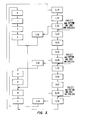
Turning now to the drawings, and in particular Fig. 1, there is illustrated a processor unit, designated generally with the reference numeral 10, constructed according to the teachings of the present invention. As illustrated, the various circuit elements of the processor unit 10 are divided into two sections, preferably, according to usage in processor operations: A "fast" section 12, containing those elements most often used in processor operations, and a "slow" section 14, containing circuit elements enjoying relatively less frequent use. As will be seen, a defining characteristic of the fast and slow sections 12, 14 is the frequency of the clock signals used to operate the respective sections. As the labels indicate, the fast section 12 will be operated with clock signals having a frequency higher than those used to operate the circuitry forming the slow section 14.
-
Continuing, the fast section 12 includes an instruction execution unit 20 coupled to memory circuits, comprising a cache memory 22 and a 32 megabyte main memory 24, by a main data bus 26 and an address bus 28. The cache memory 22 functions as the control store for the instruction execution unit 20, containing the control instructions, as well as data, that effect operation of the instruction execution unit 20.
-
The instruction execution unit 20 is of generally conventional design in that it operates in response to central instructions accessed from the cache 22 to perform the various arithmetic, logic and control functions necessary for the processor unit 10 to operate as a processor. In fact, except for those circuit elements incorporated in the processor unit 10 to form the present invention, the processor unit itself is of conventional design.
-
The main memory 24 includes address logic 30 that develops the addresses for memory access from information communicated on the main data bus 26 and the address bus 28. A memory control unit (MCU) 31 produces the signals necessary for access (e.g., read or write) with appropriate timing. Preferably, the main memory 24 is a dynamic random access memory (DRAM). Thus, MCU 31 will also produce the required refresh signals. Typically it is the cache memory 22 that is more often accessed, also via addresses communicated on the address bus 28.
-
Information as to the type of instruction being executed by the instruction execution unit 20 is produced and carried on a status (STAT) bus 32 in the form of a 4-bit nibble plus parity. Although not specifically shown, the information on the STAT bus is used by the cache memory 22, via a decode circuit (not shown), to determine when an access will be made of the cache memory 22, and the type of information that will be accessed (e.g., control instruction, data, etc.).
-
As indicated above, the slow section 14 preferably encompasses those elements of the processor unit 10 that are subject to less frequent use during processor operation, such as input/output operations. The present invention is designed for use in a multi-processor configuration in which processor- to-processor communications are conducted on redundant interprocessor buses. An illustration of such a multi-processor system can be found in U.S. Patent No. 4,228,496 or 4,888,684. The processor unit 10, therefore, includes logic for interfacing with each of the interprocessor buses (IPBs) X and Y in the form of IPB interface units 50 and 52.
-
For communication between the processor unit 10 and various peripheral units, such as additional storage in the form of magnetic disk and/or tape, printers, terminals and the like, an input/output channel (IOC) 54 connects the processor unit 10 to an I/O bus 55.
-
Also included in the slow section 14 is a maintenance diagnostic processor MDP 56. MDP 56 is a separate, special-purpose processor unit responsible for handling various maintenance/diagnostic functions to ensure the credibility of the processor unit 10. Most functions, with one exception, performed by the MDP 56 are not relevant to the present invention. That exception is the assertion of EXEC signal which, when received at multiple locations within the processor unit 10, enables operation of the processor unit.
-
The individual elements of the slow section 14, i.e., the IPBs 50, 52, the IOC 54, and the MDP 56, are coupled to one another for communication by an extended data bus 60. The elements of the slow section 14 typically do not communicate with one another, with one exception: On every slow clock cycle unused for communication between the fast and slow section 12, 14, one of the units 50 - 56 will transmit a data word on the extended data bus 60 for receipt by the other units. Data words transmitted on the extended data bus 60 (as well as the main data bus 26) are each accompanied by parity for error checking purposes. For this reason, the units of the slow section 14 communicate with one another, solely for error checking. Information transfers are conducted between the fast section 12 (i.e., the execution unit 20) and the elements of the slow section 14. For this purpose the extended data bus 60 is coupled to the main data bus 26 by a tri-state buffer unit 62 that is controlled by a 2-bit buffer control (BUFFER CTRL) signal. When BUFFER CTRL is asserted, the two data buses 26, 60 are electronically coupled to one another for communicating information from one to the other of the main and extended data buses 26, 60. BUFFER CTRL will also identify the direction of communication (e.g., from the fast section 12 to the slow section 14). When the BUFFER CTRL signal is not asserted, the main data bus 26 is effectively decoupled from the extended data bus 60 so that information flow on the extended data bus 60 will not interfere with that on the main data bus 26, and vice versa, when the two sections are operating independently.
-
According to the present invention, fast and slow sections 12, 14 are clocked by clock signals having different frequencies. It is only when information is to be passed between the two separate sections that synchronization between the clocks must be effected, and the data buses 26 and 60 intercoupled.
-
The clock signals used by each section are produced by a clock generator 70 that operates in response to a periodic, 15-nanosecond master clock signal (MCLK) produced by a master oscillator 72. The clock generator 70 produces, from MCLX, those clocking signals necessary for synchronous operation of the elements of the fast section 12 and the slow section 14. The major clocks are FAST CLK and 2XFAST CLK for the fast section 12, and SLOW CLK for the slow section 14. The IN CLK and OUT CLK signal is used to latch status information in the in-latch 80 synchronous to operation of the instruction execution unit 20, as will be described below. Similarly, the OUT CLK signal provided by the clock generator 70 operates to synchronously (relative to the slow section 14) load the out-latch 76 with address and control information.
-
The preferred embodiment of the invention has a ratio of 3:2 for the frequencies of FAST CLK to SLOW CLK although it should be evident that other ratios may be used. The FAST CLK signal is used for synchronous operation of the instruction execution unit 20, as well as other circuitry of the fast section 12, including operation of the cache and main memories 22 and 24 and associated circuitry. The 2XFAST CLK signal is used by the MCU 31 for various timing purposes.
-
The SLOW CLK is used for effecting synchronous operation of the elements of the slow section 14.
-
Digressing for a moment, synchronous operation of processor units, such as processor unit 10 (not implementing the features of the present invention) typically have state changes on one or another of the transitions between the LOW and HIGH levels of a periodic clock signal. For example, in prior conventional designs not utilizing the teachings of the present invention, data would be transferred from the instruction execution unit 20 to the IOC by the same clock signal, and relative to the same transition (e.g., LOW to HIGH) of that clock signal. Asynchronous transfers (between synchronously operated units) may be effected, obviating the need for the information transfer to occur relative to a specified clock transition, but this requires the logic to be specifically designed for such transfers, and it is a slower technique.
-
Unless otherwise specified, the major (clocked) elements of the processor 10 will change state on the LOW to HIGH transition ("rising edge") of FAST CLK (for those elements of the fast section 12), or SLOW CLK (for those elements of the slow section 14). Thus, in order for there to be a synchronous transfer of information between the fast and slow sections 12, 14, via the respective main and extended data buses 26, 60, the transfer operation (e.g., assertion of the information on the bus, accepting the information from the bus, etc.) must be conducted relative to the same rising edge. For example, assume data is to be transferred from the fast section 12 to the slow section 14 via the main and extended data buses 26, 60. The instruction that will effect that transfer begins execution (an instruction cycle) in the instruction execution unit 20, with the rising edge of FAST CLK. During that instruction cycle the data will be placed on the main/extended data bus 26/60. That data must be accepted by the slow section 12 before (or with) the next successive rising edge of FAST CLK before the next instruction cycle (initiated with the next successive rising edge of FAST CLK) will take over the main data bus 26.
-
Since there is a 3:2 ratio between the FAST CLK and SLOW CLK signals, rising edges of those two signals may not coincide when needed (e.g., see Fig. 4). Thus, the FAST CLK and SLOW CLK signals must be "synchronized;" that is, rising edges of the two signals must be made to coincide when a communication of information is to occur between the two sections 12 and 14. This, as will be seen, is the function of the clock generator 70.
-
Information transfers between the fast and slow sections 12, 14 of the processor unit 10 are not limited to utilizing the main and extended data buses 26, 60. Selection and control information is communicated from the fast section 12 to the slow section 14 via the out latch 76. Thus, a 5-bit portion of the address bus 28, and the information appearing on the STAT bus 32, are communicated to the slow section 14 via an out latch 76. The STAT information is latched in the out latch 76 with OUT CLK, from which it is passed to a decode unit 78. The decode unit 78 operates to produce the BUFFER CTRL signals that control the buffer 62 as well as the SELECT signals, carried by signal lines 79, for enabling one of the slow section functional units 50, ..., 56. The address information is conducted from the out latch 76 by a bus 80 to the elements of the slow section 14, identifying the function to be performed by the selected unit when it is placed in communication with the instruction execution unit 20.
-
Further, every information transfer cycle between the fast and slow section 12, 14 on the main and extended data buses 26, 60 invokes a return of status information from the selected unit. This return status information is communicated on three signal lines 81 from the slow section 14 to the fast section 12 via a 3-bit in-latch 80, and latched therein by the IN CLK which is synchronized to the SLOW CLK. The IN CLK, as will be explained more fully below, is present only when the FAST CLK and SLOW CLK signals are synchronized.
-
Turning now to Fig. 2A of the drawings, the clock generator 70 is illustrated in greater detail in block diagram form. As shown, the clock generator 70 includes a state machine 90 that cycles through various states, dependent upon input signals FAST ERR, EXEC, STAT, and a delayed version of EXEC, EXEC DLD. The state machine 90 is responsible for synchronizing the FAST CLK and SLOW CLK signals when information is to be transferred between the fast and slow sections of the processor unit 10 via the main and extended data buses 26, 60. A state diagram for the state machine 90 is shown in Fig. 3. Fig. 4 illustrates the various waveforms produced by the clock generator 70 when no synchronization between FAST CLK and SLOW CLK is needed. Fig. 5 illustrates the three unique waveform patterns (i.e., the three forms of synchronization that can occur - labeled A, B and C in Fig. 5) that are formed by the clock generator 70 when transitions of the FAST CLK and SLOW CLK signals are matched for synchronization.
-
With continued reference to Fig. 2A, in addition to the state machine 90, the clock generator 70 includes a state decode logic 92 that receives the 6-bit output from the state machine 90, defining each state entered by the state machine. State decode logic 92, in turn, produces, for each state assumed, the proper level for each of the signals generated by the clock generator 70.
-
Output lines 94 of the state decode logic 92, each of which carries one of the clock signals generated by the clock generator 70 (e.g., FAST CLK, IN CLK, etc.) are each applied to a respective input of a D-type flip-flop, cumulatively represented in Fig. 2A at 96. Each of the D-type flip-flops is clocked by the master clock signal (MCLX) produced by the master oscillator 72.
-
The state machine 90 will change state upon each rising transition of MCLK. As a result, the various stages of the state machine 90 most likely will change at different rates, causing the corresponding outputs of the state machine to change levels at different times. In turn, the state decode logic 92 will most likely produce multiple transitions between HI and LOW levels before settling to a signal state representative of the proper state of the state machine 90. This is the reason for the D-type flip-flops 96: To mask these transitions during each change of state machine 90. In effect, use of the D-type flip-flops will delay, one period of the MCLK signal, the actual state change, as it results in the signals produced by the clock generator 70.
-
Continuing with Fig. 2A, the clock generator 70 includes a D-type flip-flop 100 that is used to develop a delayed, synchronized version of the EXEC signal for diagnostic purposes. The EXEC signal is applied to the data (D) input of the flip-flop 100, and the SLOW CLK signal is applied to the clock (CK) input. The output (Q) of the flip-flop 100 produces the EXEC_DLD signal.
-
The EXEC signal is produced by the MDP 56 (Fig. 1) and, in effect is an enable signal that enables operation of the processor unit 10 when asserted. When not asserted, the processor unit 10 is disabled. EXEC is synchronized to the SLOW CLK signal, and is asserted/de-asserted for simultaneous start/stop of all elements of the processor unit 10 so that operation begins or ends in a consistent manner.
-
The EXEC_DLD signal is used for single-stepping the processor unit 10. Thus, the first instruction cycle following assertion of EXEC will always be a synchronized slow cycle - independent of the value carried by the STAT bus 32. The timing diagram of Fig. 2B shows the relationship between EXEC and EXEC DLD relative to SLOW CLK.
-
Fig. 3 illustrates the states assumed by the state machine 90 to produce the various signals shown in Fig. 1, including versions of FAST CLK synchronized (i.e., a LOW to HI transition aligned) with a rising edge of SLOW CLK. When there is no data bus information transfer between the fast and slow sections 12, 14, the state machine 90 will sequence through only those states labeled 0_FC, 1_FC, ... 11_FC to produce the various waveforms shown in Fig. 4. The states assumed by the state machine 90 are identified along the bottom of Fig. 4, and correspond to the states labeled in Fig. 3. As an example, the first HIGH portion 201 of the FAST CLK waveform 200 is produced by the states 0_FC, 1_FC; the immediately following LOW portion 202 of the waveform is derived from the states 2_FC, 3_FC. In similar fashion the next two successive periods of FAST CLK are produced by the states 4 FC - 7_FC and 8 FC - 11 FC. The state machine 90 returns to state 0 FC to begin over again. Each of the states 0_FC, ..., 11_FC, as well as the other states illustrated in Fig. 3, are assumed for a 15 nanosecond period, the period of the MCLK produced by the master oscillator 72.
-
A FAST CLK period is developed from four MCLK periods. Instructions are executed one per FAST CLK cycle. Fig. 3 exhibits this relationship: The twelve states 0_FC, ..., 11_FC assumed by the state machine 90 represent execution of three instructions. Thus, when the fast section 12 is operating only in the fast mode (i.e., no synchronisation with the slow section 14 is required), an instruction is executed in each of the three instruction execution cycles defined by the states 0 FC - 3_FC, 4 FC - 7_FC and 8_FC - 11_FC.
-
Each instruction execution cycle is entered assuming that it will be completed within four sequential state transitions of the state machine 90. This is a correct assumption if the FAST CLK and SLOW CLK signals do not require synchronization. If, however, the two signals require synchronization, completion of FAST CLK will require more than four states. It is during the third state of each fast clock instruction cycle (i.e., the states 2_FC, 6_FC, and 10_FC) that a determination is made of whether the instruction being executed by the instruction execution unit 20 will require an information transfer between the fast and slow sections 12, 14 - necessitating synchronization. The execution cycle will continue along the path of normal FAST CLK generation as long as the value (hex) of the four bits carried by the STAT bus 32 are not an E or an F, and the FAST_ERR signal is not asserted, and the EXEC and EXEC DLD are TRUE. If, however, an information transfer is to be made between the fast and slow sections 12, 14, rising edges of the FAST CLK and SLOW CLK signals must be aligned, i.e., the two must be synchronized. Such a transfer will be indicated by a value of E or F (hex) on the STAT bus 32.
-
As will be seen, only the FAST CLK is modified to achieve the synchronization between FAST CLK and SLOW CLK. The rising edge of FAST CLK will be delayed, relative to the immediately preceding falling edge, by an amount of time dependent upon which of the three instruction execution cycles will call for synchronization; e.g., during of the states 2_FC, 6_FC, or 10_FC it is determined that the instruction being then executed will require an information transfer between the fast and slow sections 12, 14. The SLOW CLK signal is not modified for synchronization.
-
Thus, if the determination is made during the state 2_FC that synchronization is required, the state machine will traverse from state 2 FC to 3_SC, rather than as would be normal (when synchronization is not required) to the state 3_FC. From there, (i.e., state 3_SC), the state machine 90 will pass through idle states 10 and 11, during which the level of FAST CLK is held LOW, returning to the 0_FC state to produce the next occurring rising edge 206 (Fig. 5) of the FAST CLK waveform 200a. Note, as Fig. 5 indicates, that the rising edge 204 of SLOW CLK coincides with the rising edge 206 of FAST CLK. Without the travel of the state machine 90 through the additional states 3_SC, 10, and 11, the rising edge would have occurred during the fast clock state 4_FC, approximately 30 nanoseconds (two MCLK periods) before that of SLOW CLK (see Fig. 4). Note also that 2XFAST CLK is also modified to align the rising transition of that signal with SLOW CLK and FAST CLK.
-
Similarly, if the determination is made by the state machine 90 that the instruction being executed during the instruction cycle of fast clock states 4_FC - 7_FC is made, the third state, 6_FC, of that execution cycle will be followed by the delay states 7_SC, 8, 9, 10 and 11 (i.e., waveform pattern B, Fig. 5), as Fig. 3 indicates. Note that there are too additional states, 8 and 9, traversed, when compared to the delay added to the execution cycle of 0_FC - 3 FC. This is the result, again, of the phase relationships between the FAST CLK and SLOW CLK signals that exist at the time the determination is made. Similarly, the longest delay for synchronization of rising edges of the FAST CLK and SLOW CLK signals are produced if the determination for the necessity of synchronization is made during the state (10_FC). The state machine 90 then passes through the states 11 SC, 0, 1, 2, 3, 10 and 11, as indicated in Fig. 3 (and Fig. 5 - waveform pattern C).
-
Selection of the synchronization path depends upon the state of several signals applied to the state machine 90, as indicated in Fig. 3. First, is the information carried by the STAT bus 32. If the instruction execution unit 20 is executing an instruction that will use the extended data bus 60, the state of the STAT bus 32 will be an E or an F (hex). If it is anything else, the next state assumed by the state machine 90 will be 3_FC, 7_FC, or 11_FC (assuming the other signals, discussed below, permit this change).
-
EXEC, as explained above, enables operation of the processor unit. If EXEC is LOW, the processor unit 10 is disabled and not operating. This does not mean, however, that clock signals need not be generated. The main memory, for example, will need to maintain its refresh cycle. Thus, even though the processor is disabled, with EXEC not asserted, the FAST CLK signal continues, but in the slow cycle loop 0_FC, 1_FC, 2_FC, 3_SC, 10 and 11.
-
The processor unit 10 contains, in both the fast and slow sections 12 and 14, circuitry (not shown) that will monitor various operating parameters. If this circuitry detects an error, an error flag of one sort or another will be raised. When such error detection occurs, is desirable to halt operation of the processor unit. In the case of the present invention, it is desirable to halt the fast and slow sections 12, 14 at the same time, i.e., on the same rising edge. Thus, when one of the error conditions occur within the fast section 12, the FAST_ERR signal will be asserted to halt operation of the processor unit 10. When asserted, the FAST ERR signal will cause the state machine 90 to take one of the synchronization paths, so that when the rising edges of FAST CLK and SLOW CLK coincide, EXEC can be dropped, thereby halting both sections at the same time.
-
Many of today's data processing systems are designed to include circuitry for diagnostic operation, and the processor unit 10 is no exception. One such diagnostic is the ability to perform single-step operation; that is, to let the instruction execution unit 20 execute one instruction and then to stop operation. To do this, the MDP 56 will raise the EXEC signal for one execution cycle, and bring it down at the completion of that cycle. Since EXEC was LOW prior to its assertion, its derivative, EXEC DLD, developed by the flip-flop 100, will also be LOW. The purpose of the delayed version of EXEC, EXEC_DLD, is to ensure that the single-step operation of the fast section 12 will be a slow cycle and terminate with that of the slow section. Thus, when EXEC is raised (with the rising edge of SLOW CLK, since the MDP is clocked by SLOW CLK), the fact that EXEC DLD is LOW will ensure that a desired slow cycle is taken. When the single-step operation is completed, the MDP 56 will bring down EXEC and the state machine will remain locked into a slow cycle routine (e.g., for memory refresh operation, as explained above) until EXEC is again asserted.
-
Returning for the moment to Fig. 1, note that the IN CLK signal operates the in-latch 80 to temporarily store three bits of information (e.g., interrupts, status, and the like) communicated from the slow section 14. As mentioned above, the latching operation is synchronized to operation of the execution unit 20, i.e., to the FAST CLK signal. Accordingly, as illustrated in Figs. 4 and 5 by the waveforms 208 and 210, the IN CLK signal is produced by (1) the idle states 10 and 11, (2) the fast clock states 10_FC and 11_FC, or (3) the fast clock state 10_FC and the initial synchronizing state 11_SC. Latches used in the design of the present invention are level-sensitive, and are of the type in which the outputs follow the inputs while the control signal is HIGH; and the input is latched when the control signal goes LOW. Since it is obviously undesirable to have the output of a latch changing state when it is attempted to be read, the need for synchronizing the in-latch 80 to operation of the instruction execution unit 20 is evident. Thus, the IN CLK signal is produced, relative to FAST CLK, so that data will be held steady in the in-latch 80 a sufficient set-up time for the destination circuits (e.g., instruction execution 20).
-
In similar fashion, the out latch 76 is synchronized to the operation of the elements of the slow section 14. When there is no synchronizing activity between the FAST CLK and SLOW CLK signals, the OUT CLK is produced by the fast clock states 0 FC - 1_FC and 6 FC - 7_FC. Depending upon the synchronization cycle assumed, the OUT CLK signal will also be produced by the states 6FC - 7 SC and the idle states 0 - 1. The information carried by the address and STAT buses 28, 32 will change on the rising edge (LOW to HIGH transition) of FAST CLK. But the slow section 14 elements, being edge-triggered devices (as are most elements of the fast section 12) accept the information on the rising edge of SLOW CLK. Thus, OUT CLK holds the data in the out-latch 76 steady to allow it to set up for rising edges of SLOW CLK; thereafter, OUT CLK goes HIGH, permitting the output of the out-latch 76 to follow the input. See Fig. 5.