EP0477566A2 - Improvements in or relating to light modulation - Google Patents
Improvements in or relating to light modulation Download PDFInfo
- Publication number
- EP0477566A2 EP0477566A2 EP91114435A EP91114435A EP0477566A2 EP 0477566 A2 EP0477566 A2 EP 0477566A2 EP 91114435 A EP91114435 A EP 91114435A EP 91114435 A EP91114435 A EP 91114435A EP 0477566 A2 EP0477566 A2 EP 0477566A2
- Authority
- EP
- European Patent Office
- Prior art keywords
- modulation
- modulating
- elements
- modulating elements
- amplitude
- Prior art date
- Legal status (The legal status is an assumption and is not a legal conclusion. Google has not performed a legal analysis and makes no representation as to the accuracy of the status listed.)
- Granted
Links
Images

Classifications
-
- G—PHYSICS
- G02—OPTICS
- G02F—OPTICAL DEVICES OR ARRANGEMENTS FOR THE CONTROL OF LIGHT BY MODIFICATION OF THE OPTICAL PROPERTIES OF THE MEDIA OF THE ELEMENTS INVOLVED THEREIN; NON-LINEAR OPTICS; FREQUENCY-CHANGING OF LIGHT; OPTICAL LOGIC ELEMENTS; OPTICAL ANALOGUE/DIGITAL CONVERTERS
- G02F2/00—Demodulating light; Transferring the modulation of modulated light; Frequency-changing of light
-
- G—PHYSICS
- G09—EDUCATION; CRYPTOGRAPHY; DISPLAY; ADVERTISING; SEALS
- G09G—ARRANGEMENTS OR CIRCUITS FOR CONTROL OF INDICATING DEVICES USING STATIC MEANS TO PRESENT VARIABLE INFORMATION
- G09G3/00—Control arrangements or circuits, of interest only in connection with visual indicators other than cathode-ray tubes
- G09G3/20—Control arrangements or circuits, of interest only in connection with visual indicators other than cathode-ray tubes for presentation of an assembly of a number of characters, e.g. a page, by composing the assembly by combination of individual elements arranged in a matrix no fixed position being assigned to or needed to be assigned to the individual characters or partial characters
- G09G3/34—Control arrangements or circuits, of interest only in connection with visual indicators other than cathode-ray tubes for presentation of an assembly of a number of characters, e.g. a page, by composing the assembly by combination of individual elements arranged in a matrix no fixed position being assigned to or needed to be assigned to the individual characters or partial characters by control of light from an independent source
- G09G3/3433—Control arrangements or circuits, of interest only in connection with visual indicators other than cathode-ray tubes for presentation of an assembly of a number of characters, e.g. a page, by composing the assembly by combination of individual elements arranged in a matrix no fixed position being assigned to or needed to be assigned to the individual characters or partial characters by control of light from an independent source using light modulating elements actuated by an electric field and being other than liquid crystal devices and electrochromic devices
- G09G3/346—Control arrangements or circuits, of interest only in connection with visual indicators other than cathode-ray tubes for presentation of an assembly of a number of characters, e.g. a page, by composing the assembly by combination of individual elements arranged in a matrix no fixed position being assigned to or needed to be assigned to the individual characters or partial characters by control of light from an independent source using light modulating elements actuated by an electric field and being other than liquid crystal devices and electrochromic devices based on modulation of the reflection angle, e.g. micromirrors
-
- G—PHYSICS
- G02—OPTICS
- G02B—OPTICAL ELEMENTS, SYSTEMS OR APPARATUS
- G02B26/00—Optical devices or arrangements for the control of light using movable or deformable optical elements
- G02B26/001—Optical devices or arrangements for the control of light using movable or deformable optical elements based on interference in an adjustable optical cavity
-
- G—PHYSICS
- G02—OPTICS
- G02B—OPTICAL ELEMENTS, SYSTEMS OR APPARATUS
- G02B26/00—Optical devices or arrangements for the control of light using movable or deformable optical elements
- G02B26/06—Optical devices or arrangements for the control of light using movable or deformable optical elements for controlling the phase of light
-
- G—PHYSICS
- G02—OPTICS
- G02B—OPTICAL ELEMENTS, SYSTEMS OR APPARATUS
- G02B26/00—Optical devices or arrangements for the control of light using movable or deformable optical elements
- G02B26/08—Optical devices or arrangements for the control of light using movable or deformable optical elements for controlling the direction of light
- G02B26/0816—Optical devices or arrangements for the control of light using movable or deformable optical elements for controlling the direction of light by means of one or more reflecting elements
- G02B26/0833—Optical devices or arrangements for the control of light using movable or deformable optical elements for controlling the direction of light by means of one or more reflecting elements the reflecting element being a micromechanical device, e.g. a MEMS mirror, DMD
- G02B26/0841—Optical devices or arrangements for the control of light using movable or deformable optical elements for controlling the direction of light by means of one or more reflecting elements the reflecting element being a micromechanical device, e.g. a MEMS mirror, DMD the reflecting element being moved or deformed by electrostatic means
-
- G—PHYSICS
- G09—EDUCATION; CRYPTOGRAPHY; DISPLAY; ADVERTISING; SEALS
- G09F—DISPLAYING; ADVERTISING; SIGNS; LABELS OR NAME-PLATES; SEALS
- G09F9/00—Indicating arrangements for variable information in which the information is built-up on a support by selection or combination of individual elements
- G09F9/30—Indicating arrangements for variable information in which the information is built-up on a support by selection or combination of individual elements in which the desired character or characters are formed by combining individual elements
- G09F9/37—Indicating arrangements for variable information in which the information is built-up on a support by selection or combination of individual elements in which the desired character or characters are formed by combining individual elements being movable elements
- G09F9/372—Indicating arrangements for variable information in which the information is built-up on a support by selection or combination of individual elements in which the desired character or characters are formed by combining individual elements being movable elements the positions of the elements being controlled by the application of an electric field
-
- G—PHYSICS
- G09—EDUCATION; CRYPTOGRAPHY; DISPLAY; ADVERTISING; SEALS
- G09G—ARRANGEMENTS OR CIRCUITS FOR CONTROL OF INDICATING DEVICES USING STATIC MEANS TO PRESENT VARIABLE INFORMATION
- G09G2300/00—Aspects of the constitution of display devices
- G09G2300/04—Structural and physical details of display devices
- G09G2300/0439—Pixel structures
- G09G2300/0443—Pixel structures with several sub-pixels for the same colour in a pixel, not specifically used to display gradations
Definitions
- the desired amplitude, A, and net phase angle, ⁇ must be selected. Once those two variables are set, the angles for the individual modulating elements must be determined, in step 110.
- the complete analytical description of the optical distribution transmitted by, or reflected by, the full complex pixel is given by equation (1): where w x and w y are the widths of the modulating elements in the horizontal and vertical direction, W is the width of the entire square pixel region, and ⁇ 1 and ⁇ 2 are the phase setting of the individual modulators.
Abstract
Description
- The present invention relates to methods of light modulation and spatial light modulators, including phase modulators and full complex light modulators.
- Spatial light modulators (SLMs) are devices used to control the distribution of light in an optical system. Spatial light modulators are divided into one- or two-dimensional arrays of modulation elements called pixels, or picture elements, that represent the smallest addressable unit within the device. The SLM pixel is used to modify either the amplitude or the phase of the light distribution within the optical system.
- In practice, the light modulation characteristics of most prior art SLMs are coupled combinations of amplitude and phase changes. The modulation characteristic of a pixel is controlled by a single applied signal, either an electrical voltage, current or incident optical intensity level, so the amplitude and phase characteristics of the pixel can not be independently set.
- There are numerous applications, especially in optical information processing, in which controlling amplitude and phase independently is essential. Phase modulation is essential since most of the signal information is contained in the phase terms. The additional control of amplitude provides means for rejecting noise in the filter plane for improved system performance.
- Four major types of modulators are presently being used for phase modulation; liquid crystal, photorefractive, magnetooptic, and deformable mirror. All have coupled phase and amplitude modulation characteristics.
- Liquid crystals allow for phase and amplitude modulation, but phase modulation has extremely narrow ranges for the electric fields applied for uniform realignment, making it hard to control. Amplitude modulation is also difficult since the nonuniform realignment causing the amplitude modulation also contributes to phase modulation, resulting in a phase-amplitude coupled modulation.
- Photorefractive modulators work for phase-only modulation only at extremely high voltages. Birefringence caused in nonuniform alignment produces amplitude modulation. But since photorefractive, like liquid crystal, modulates by a change in the refractive index, phase modulation accompanies amplitude modulation.
- Magnetooptic modulators produce a binary change in the polarization of light, but are hard to control in operation. Kast, et al., in their article in Applied Optics, 15 March 1989, describe a method for ternary operation of magnetooptic modulators, but it has a very limited range of amplitude- or phase-only modulations, none of which are independently controlled.
- Present deformable mirror devices could be effective if the resolution of the optical system was fine enough to resolve the mirror element separate from the background. But, the normal setting for resolution of optical systems is the Nyquist frequency, causing the mirror to be mixed with the background. Amplitude modulation results from the interference between the two distributions.
- Two other methods of phase-only modulation have been used. The first method was introduced by Brown and Lohmann in Applied Optics, 1966. Their technique, detour phase, requires very tight system alignment and limited field-of-view for the phase encoding approximations to be valid. The second was introduced by Hansche, et al., in their article in Applied Optics, 15 November, 1989. Their approach allows for different amplitudes to be produced, but requires a lowered resolution in the optical system.
- According to the present invention in a first aspect thereof, a method for modulation of light comprises the following steps:
- a) dividing a picture element into a number of modulating elements;
- b) providing addressing circuitry for each said modulating element;
- c) selecting the desired phase angle and amplitude of modulation;
- d) determining appropriate displacement angles of said modulating elements to achieve said phase angle and amplitude;
- e) addressing said modulating elements to achieve desired angle; and
- f) resolving said modulation elements as said picture element preferably said addressing of said modulating elements consists of applying a predetermined voltage to an electrode; located directly under said modulating element. The said modulation may be amplitude modulation or full complex modulation.
- According to the present invention in a second output thereof a spatial light modulator, comprises:
- a) a plurality of picture elements formed in a layered structure, each pixel being divided into a number of modulating elements;
- b) said layered structure including a substrate, a spacer layer on said substrate, a reflecting layer on said spacer, and electrical addressing circuitry;
- c) each of said modulating elements being an electrostatically deflectable element formed in said reflecting layer, and said spacer defining a well located between said deflectable element and a plurality of activation electrodes arranged to affect said electrostatic deflection; and
- d) electrical addressing circuitry such that each of said modulating elements are independently addressable.
- As part of this application an exemplary method and apparatus for full complex light modulation is described. Full complex light modulation allows the modulation of a signal with independent control of phase and amplitude.
- The method described uses a standard picture element. The picture element is then divided into a number of smaller modulating elements. Each modulating element is provided with its own circuitry for addressing. The net phase angle, Φ, and the desired resultant amplitude, A, must be selected. Through a series of calculations using A and Φ, a number of angles can be found. These angles, ϑ₁, ϑ₂, etc. are for the individual modulating elements.
- The addressing circuitry for the individual modulating elements is then activated in such a way as to cause the modulation at the angle ϑx. The light signal is then directed to the picture element and its individual modulating elements. The final step in the process occurs when the optical system scans the modulating elements and resolves them as if they were the whole picture element.
- The preferred embodiment shown uses a deformable mirror device (DMD) as the picture element. A flexure beam DMD is cut into a number, for example two, of smaller flexure beam DMDs. The addressing circuitry in this case is electrodes, which are located underneath each half of the picture element. The angles, ϑ₁, and ϑ₂, are caused when a voltage is applied to the electrodes. The value of the voltage applied determines the value of the angle. The preferred embodiment shows only two modulating elements but it is possible to use this method for more than two angles.
- For a more complete understanding of the present invention, and the advantages thereof, reference is now made to the following description, given by way of example only, taken in conjunction with the accompanying drawings, in which:
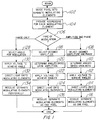
- FIGURE 1 shows the flow chart of the process for full complex light modulation;
- FIGURE 2 shows a perspective view of a prior art flexure beam deformable mirror device (DMD);
- FIGURE 3 shows a perspective view of a divided flexure beam DMD according to the present invention;
- FIGURE 4 is a top view of the divided DMD; and
- FIGURE 5 shows one example of a DMD divided into more than two modulating element.
- The flowchart for the process of full complex light modulation is illustrated in FIGURE 1. In
step 102, the pixel is divided into however many modulating elements are desired within a pixel. Step 104 provides for addressing circuitry for each modulating element within the pixel, so each is individually addressable. Step 106 is the point at which the type of modulation must be selected. - If amplitude and phase modulation is desired, it is possible to perform both simultaneously. The process continues in this case to step 108.
- In this step, the desired amplitude, A, and net phase angle, Φ, must be selected. Once those two variables are set, the angles for the individual modulating elements must be determined, in
step 110. The complete analytical description of the optical distribution transmitted by, or reflected by, the full complex pixel is given by equation (1):
where wx and wy are the widths of the modulating elements in the horizontal and vertical direction, W is the width of the entire square pixel region, and ϑ₁ and ϑ₂ are the phase setting of the individual modulators. - With the optical system resolution set to pass the 0,0 diffraction order Nyquist passband for array elements of width W, the net response of this pixel is determined by equation (2):

where the asterisk represents a two-dimensional convolution. This equation represents a complicated spatial distribution that cannot be simplified. However, the distribution is essentially a two-dimensional sinc function of width slightly greater that 2W and a peak complex amplitude given by equation (3):

where A and Φ are the amplitude and phase values of the net pixel response resulting from the coherent mixing of the two phase modulator responses. - At any specific net phase value Φ, there is a maximum possible net amplitude, A. The maximum value occurs when the two modulator phase settings are equal,
ϑ₁ = ϑ₂ = ϑ giving:

However, to specify this maximum value, it is first necessary to determine the proper phase setting ϑ to find the net phase angle Φ. The geometrical analysis to make this determination is quite involved resulting in the following relationship
This expression gives two values for the phase angle ϑ corresponding to angles in the upper or lower half plane. The proper choice is the angle that lies in the same half plane as Φ. The geometrical analysis again gives the prescription for specifying the phase settings, ϑ₁ and ϑ₂, to achieve the desired net amplitude and phase values, A and Φ. These phase settings are


where
and
These formulas are the specific ones for two halves of a given pixel. It is possible to use this method of analysis for more than two angles. - Step 112 requires the application of the voltages in order to deflect the appropriate modulating elements to achieve the phase angles calculated in
step 110. The voltage to achieve a certain angle can be found by the following relationship:
where V is the applied voltage, K is the spring constant of the DMD hinge, ϑ is the angle of deflection, d₀ is the distance of the DMD from the electrode before deflection, λ is the wavelength of the incident light, and ε₀ is the electrical permittivity of free space. - Step 114 is the part of the process that an actual optical signal is applied to the set elements by the system. Step 116 allows all of the independently addressed modulating elements to be integrated into one pixel. In this context, integration is the actual scanning done by the optical system, where the individual elements are grouped back into the original pixel. That is, the modulating elements, taken together are scanned by the optical system as though they were a single pixel.
- If amplitude-only modulation is desired, the process steps to 118. The modulated amplitude, A, is selected. Using equations 6, 7, 8, and 9, it is possible to again solve for the individual angles, ϑ₁ and ϑ₂, in step 120. The relationship for the voltage set out in equation 10 is again used to determine the amount of applied voltage necessary for the proper deflection and applied in step 122. Step 124 again requires the direction of light, and step 126 is the integration of the modulation elements into the original pixel.
- With the embodiment described phase-only modulation is also possible. The process moves to step 128. The angle selected for phase modulation is the angle for the individual modulating elements. Using equation 10 to determine the proper voltage, all individual modulating elements are set to that angle in step 130. After directing the light onto the modulating elements in step 132, each individual piece of the original pixel is treated as its own pixel. For example, if there existed an original array of N x N pixels, and each pixel was divided into two modulating elements, the system would scan an array of N x 2N pixels at step 134.
- FIGURE 2 shows a prior art configuration of a flexure beam DMD. An addressing
electrode 206 is built onto asubstrate 202. Amirror element 210 is built onto a spacer covering the layer containing 206. The spacer layer is then etched away. This leaves a layer of support posts 204A, 204B, 204C, and 204D, with an gap between themirror element 210 and theelectrode 206. When a pre-determined voltage is applied toelectrode 206,mirror element 210 is electrostatically attracted to it. The flexure hinges 208A, 208B, 208C, and 208D, allow the mirror to deflect downwards. Because all four corners are supported, the mirror deflects with a piston-like movement. - FIGURE 3 illustrates a divided DMD with two individual modulating elements. If a voltage is applied to address
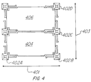
electrodes 302, then mirror 310 will deflect downwards flexing onhinges Mirror 312 will not deflect unless a voltage is applied to addresselectrode 310, allowing independent operation of the two mirror elements. As in FIGURE 2, the flexure hinges 306A, 306B, 306C, 306D, 306E, and 306F, are supported bysupport posts mirror elements electrodes - The top view of the divided pixel is shown in FIGURE 4. The variables used in the above equations are shown. Wx is along the horizontal axis, as indicated by the double-headed
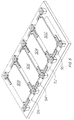
arrow 401, the distance from support post 402A to supportpost 402B. Wy is along the vertical axis, indicated by the double-headed arrow 403, either fromsupport post 402B to 402C, or from support post 402C to support post 402D. In this case, the pixel was divided horizontally into two parts, so there are two wy to one wx.Mirror elements - FIGURE 5 shows an example of one possible other division of a pixel. The pixel is divided into two individual elements, which are in turn divided into two pieces. The
mirror 502 has addressingelectrode 510, and each other modulating element has a corresponding element, making all of them individually addressable. - A feature of the present invention is that it may be applied to existing systems by replacing picture elements with divided picture elements in accordance with the present invention, for example prior art DMDs with divided DMDs. The optical arrangement of such existing system will inherently resolve such a divided pixel as a single picture atempt. Thus full complex modulation capability may be added to the existing system.
said modulator is divided into two halves. Advantageously said addressing circuitry includes a plurality of activation electrodes; one electrode corresponding to each modulating element.
Claims (9)
- A method for modulation of light comprising the following steps:a) dividing a picture element into a number of modulating elements;b) providing addressing circuitry for each said modulating element;c) selecting the desired phase angle and amplitude of modulation;d) determining appropriate displacement angles of said modulating elements to achieve said phase angle and amplitude;e) addressing said modulating elements to achieve desired angle; andf) resolving said modulation elements as said picture element.
- The method of claim 1, wherein:a) said addressing of said modulating elements consists of applying a predetermined voltage to an electrode; located directly under said modulating element.
- A method as claimed in claim 1 or claim 2 and wherein said modulation is amplitude modulation.
- A method as claimed in claim 1 or claim 2 and wherein said modulation is full complex modulation.
- A spatial light modulator, comprising:a) a plurality of picture elements formed in a layered structure, each pixel being divided into a number of modulating elements;b) said layered structure including a substrate, a spacer layer on said substrate, a reflecting layer on said spacer, and electrical addressing circuitry;c) each of said modulating elements being an electrostatically deflectable element formed in said reflecting layer, and said spacer defining a well located between said deflectable element and a plurality of activation electrodes arranged to affect said electrostatic deflection; andd) electrical addressing circuitry such that each of said modulating elements are independently addressable.
- The modulator of claim 5, wherein:a) said modulator is divided into two halves.
- The modulator of claim 1, 5 or claim 6, wherein:a) said addressing circuitry includes a plurality of activation electrodes; one electrode corresponding to each modulating element.
- A picture element modulator divided into a number of individual modulating elements.
- A deformable mirror device divided into a number of individual modulating elements.
Applications Claiming Priority (2)
| Application Number | Priority Date | Filing Date | Title |
|---|---|---|---|
| US07/590,405 US5148157A (en) | 1990-09-28 | 1990-09-28 | Spatial light modulator with full complex light modulation capability |
| US590405 | 1990-09-28 |
Publications (3)
| Publication Number | Publication Date |
|---|---|
| EP0477566A2 true EP0477566A2 (en) | 1992-04-01 |
| EP0477566A3 EP0477566A3 (en) | 1992-05-13 |
| EP0477566B1 EP0477566B1 (en) | 1996-12-18 |
Family
ID=24362124
Family Applications (1)
| Application Number | Title | Priority Date | Filing Date |
|---|---|---|---|
| EP91114435A Expired - Lifetime EP0477566B1 (en) | 1990-09-28 | 1991-08-28 | Improvements in or relating to light modulation |
Country Status (5)
| Country | Link |
|---|---|
| US (1) | US5148157A (en) |
| EP (1) | EP0477566B1 (en) |
| JP (1) | JP3155307B2 (en) |
| KR (1) | KR100231123B1 (en) |
| DE (1) | DE69123676T2 (en) |
Cited By (21)
| Publication number | Priority date | Publication date | Assignee | Title |
|---|---|---|---|---|
| EP0539889A2 (en) * | 1991-10-30 | 1993-05-05 | Steinbichler, Hans, Dr. | Micromechanical actuator |
| EP0568801A1 (en) * | 1992-04-03 | 1993-11-10 | Texas Instruments Incorporated | Methods for multiple phase light modulation, systems and devices |
| EP0657760A1 (en) * | 1993-09-15 | 1995-06-14 | Texas Instruments Incorporated | Image simulation and projection system |
| WO1999067671A1 (en) * | 1998-06-24 | 1999-12-29 | Silicon Light Machines | Method and apparatus for modulating an incident light beam for forming a two-dimensional image |
| EP1215168A1 (en) * | 2000-12-07 | 2002-06-19 | Agere Systems Guardian Corporation | Magnetically packaged optical mems device and method for making the same |
| US6714337B1 (en) | 2002-06-28 | 2004-03-30 | Silicon Light Machines | Method and device for modulating a light beam and having an improved gamma response |
| US6712480B1 (en) | 2002-09-27 | 2004-03-30 | Silicon Light Machines | Controlled curvature of stressed micro-structures |
| US6767751B2 (en) | 2002-05-28 | 2004-07-27 | Silicon Light Machines, Inc. | Integrated driver process flow |
| US6782205B2 (en) | 2001-06-25 | 2004-08-24 | Silicon Light Machines | Method and apparatus for dynamic equalization in wavelength division multiplexing |
| US6785001B2 (en) | 2001-08-21 | 2004-08-31 | Silicon Light Machines, Inc. | Method and apparatus for measuring wavelength jitter of light signal |
| US6801354B1 (en) | 2002-08-20 | 2004-10-05 | Silicon Light Machines, Inc. | 2-D diffraction grating for substantially eliminating polarization dependent losses |
| US6800238B1 (en) | 2002-01-15 | 2004-10-05 | Silicon Light Machines, Inc. | Method for domain patterning in low coercive field ferroelectrics |
| US6806997B1 (en) | 2003-02-28 | 2004-10-19 | Silicon Light Machines, Inc. | Patterned diffractive light modulator ribbon for PDL reduction |
| US6813059B2 (en) | 2002-06-28 | 2004-11-02 | Silicon Light Machines, Inc. | Reduced formation of asperities in contact micro-structures |
| US6829077B1 (en) | 2003-02-28 | 2004-12-07 | Silicon Light Machines, Inc. | Diffractive light modulator with dynamically rotatable diffraction plane |
| US6829092B2 (en) | 2001-08-15 | 2004-12-07 | Silicon Light Machines, Inc. | Blazed grating light valve |
| US6839479B2 (en) | 2002-05-29 | 2005-01-04 | Silicon Light Machines Corporation | Optical switch |
| US7046420B1 (en) | 2003-02-28 | 2006-05-16 | Silicon Light Machines Corporation | MEM micro-structures and methods of making the same |
| WO2007044528A1 (en) * | 2005-10-07 | 2007-04-19 | Lucent Technologies Inc. | Apparatus for modulating one or both of spectral phase and amplitude of an optical signal |
| WO2009130603A2 (en) * | 2008-04-24 | 2009-10-29 | Micronic Laser Systems Ab | Spatial light modulator with structured mirror surfaces |
| US8472103B2 (en) | 2007-10-19 | 2013-06-25 | Seereal Technologies S.A. | Complex-valued spatial light modulator |
Families Citing this family (71)
| Publication number | Priority date | Publication date | Assignee | Title |
|---|---|---|---|---|
| US5083857A (en) * | 1990-06-29 | 1992-01-28 | Texas Instruments Incorporated | Multi-level deformable mirror device |
| GB9024979D0 (en) * | 1990-11-16 | 1991-01-02 | Rank Cintel Ltd | Digital mirror spatial light modulator |
| US6219015B1 (en) | 1992-04-28 | 2001-04-17 | The Board Of Directors Of The Leland Stanford, Junior University | Method and apparatus for using an array of grating light valves to produce multicolor optical images |
| US5416618A (en) * | 1992-11-10 | 1995-05-16 | The United States Of America As Represented By The Administrator Of The National Aeronautics & Space Administration | Full complex modulation using two one-parameter spatial light modulators |
| US6674562B1 (en) | 1994-05-05 | 2004-01-06 | Iridigm Display Corporation | Interferometric modulation of radiation |
| US5457493A (en) * | 1993-09-15 | 1995-10-10 | Texas Instruments Incorporated | Digital micro-mirror based image simulation system |
| US7460291B2 (en) * | 1994-05-05 | 2008-12-02 | Idc, Llc | Separable modulator |
| US7138984B1 (en) | 2001-06-05 | 2006-11-21 | Idc, Llc | Directly laminated touch sensitive screen |
| US6680792B2 (en) * | 1994-05-05 | 2004-01-20 | Iridigm Display Corporation | Interferometric modulation of radiation |
| US5793600A (en) * | 1994-05-16 | 1998-08-11 | Texas Instruments Incorporated | Method for forming high dielectric capacitor electrode structure and semiconductor memory devices |
| US5712912A (en) * | 1995-07-28 | 1998-01-27 | Mytec Technologies Inc. | Method and apparatus for securely handling a personal identification number or cryptographic key using biometric techniques |
| US6560018B1 (en) * | 1994-10-27 | 2003-05-06 | Massachusetts Institute Of Technology | Illumination system for transmissive light valve displays |
| US5841579A (en) | 1995-06-07 | 1998-11-24 | Silicon Light Machines | Flat diffraction grating light valve |
| US5740276A (en) * | 1995-07-27 | 1998-04-14 | Mytec Technologies Inc. | Holographic method for encrypting and decrypting information using a fingerprint |
| US6525750B1 (en) | 1996-03-08 | 2003-02-25 | Duke University | Projection display for computers |
| US5768242A (en) * | 1996-04-05 | 1998-06-16 | The United States Of America As Representd By The Administrator Of The National Aeronautics And Space Administration | Apparatus and method for focusing a light beam in a three-dimensional recording medium by a dynamic holographic device |
| US5833360A (en) * | 1996-10-17 | 1998-11-10 | Compaq Computer Corporation | High efficiency lamp apparatus for producing a beam of polarized light |
| US6390626B2 (en) | 1996-10-17 | 2002-05-21 | Duke University | Image projection system engine assembly |
| US6243152B1 (en) | 1996-12-17 | 2001-06-05 | Duke University | Contrast polymer dispersed liquid crystal projection display system |
| US5868480A (en) * | 1996-12-17 | 1999-02-09 | Compaq Computer Corporation | Image projection apparatus for producing an image supplied by parallel transmitted colored light |
| US5977942A (en) * | 1996-12-20 | 1999-11-02 | Compaq Computer Corporation | Multiplexed display element sequential color LCD panel |
| US6313893B1 (en) | 1996-12-27 | 2001-11-06 | Duke University | Compensation for DC balancing of liquid crystal displays |
| US5982553A (en) | 1997-03-20 | 1999-11-09 | Silicon Light Machines | Display device incorporating one-dimensional grating light-valve array |
| CA2203212A1 (en) | 1997-04-21 | 1998-10-21 | Vijayakumar Bhagavatula | Methodology for biometric encryption |
| US5867251A (en) * | 1997-05-02 | 1999-02-02 | The General Hospital Corp. | Scanning ophthalmoscope with spatial light modulators |
| US5963367A (en) * | 1997-09-23 | 1999-10-05 | Lucent Technologies, Inc. | Micromechanical xyz stage for use with optical elements |
| US6088102A (en) | 1997-10-31 | 2000-07-11 | Silicon Light Machines | Display apparatus including grating light-valve array and interferometric optical system |
| SE9800665D0 (en) * | 1998-03-02 | 1998-03-02 | Micronic Laser Systems Ab | Improved method for projection printing using a micromirror SLM |
| US6816302B2 (en) | 1998-03-02 | 2004-11-09 | Micronic Laser Systems Ab | Pattern generator |
| WO1999052006A2 (en) | 1998-04-08 | 1999-10-14 | Etalon, Inc. | Interferometric modulation of radiation |
| US8928967B2 (en) | 1998-04-08 | 2015-01-06 | Qualcomm Mems Technologies, Inc. | Method and device for modulating light |
| US6271808B1 (en) | 1998-06-05 | 2001-08-07 | Silicon Light Machines | Stereo head mounted display using a single display device |
| US6130770A (en) | 1998-06-23 | 2000-10-10 | Silicon Light Machines | Electron gun activated grating light valve |
| US6101036A (en) | 1998-06-23 | 2000-08-08 | Silicon Light Machines | Embossed diffraction grating alone and in combination with changeable image display |
| US6303986B1 (en) | 1998-07-29 | 2001-10-16 | Silicon Light Machines | Method of and apparatus for sealing an hermetic lid to a semiconductor die |
| US6624880B2 (en) | 2001-01-18 | 2003-09-23 | Micronic Laser Systems Ab | Method and apparatus for microlithography |
| JP2002331416A (en) * | 2001-05-08 | 2002-11-19 | Ogura:Kk | Bar-shaped member cutter |
| US6747781B2 (en) | 2001-06-25 | 2004-06-08 | Silicon Light Machines, Inc. | Method, apparatus, and diffuser for reducing laser speckle |
| US6485150B1 (en) | 2001-07-03 | 2002-11-26 | The United States Of America As Represented By The Secretary Of The Navy | Tunable spectral source |
| CN100410725C (en) * | 2001-09-12 | 2008-08-13 | 麦克罗尼克激光系统公司 | Improved method and apparatus using an SLM |
| US6618185B2 (en) * | 2001-11-28 | 2003-09-09 | Micronic Laser Systems Ab | Defective pixel compensation method |
| US6950194B2 (en) * | 2001-12-07 | 2005-09-27 | Micronic Laser Systems Ab | Alignment sensor |
| SE0104238D0 (en) * | 2001-12-14 | 2001-12-14 | Micronic Laser Systems Ab | Method and apparatus for patterning a workpiece |
| US7106490B2 (en) * | 2001-12-14 | 2006-09-12 | Micronic Laser Systems Ab | Methods and systems for improved boundary contrast |
| US20030233630A1 (en) * | 2001-12-14 | 2003-12-18 | Torbjorn Sandstrom | Methods and systems for process control of corner feature embellishment |
| US6573850B1 (en) | 2002-05-24 | 2003-06-03 | Wolfson Microelectronics Limited | Digital-to-analogue converter circuits |
| US6728023B1 (en) | 2002-05-28 | 2004-04-27 | Silicon Light Machines | Optical device arrays with optimized image resolution |
| US6822797B1 (en) | 2002-05-31 | 2004-11-23 | Silicon Light Machines, Inc. | Light modulator structure for producing high-contrast operation using zero-order light |
| US6829258B1 (en) | 2002-06-26 | 2004-12-07 | Silicon Light Machines, Inc. | Rapidly tunable external cavity laser |
| CN1695150B (en) * | 2002-10-01 | 2011-06-15 | 麦克罗尼克激光系统公司 | Methods and systems for process control of corner feature embellishment |
| US7755657B2 (en) | 2003-06-12 | 2010-07-13 | Micronic Laser Systems Ab | Method for high precision printing of patterns |
| US6833854B1 (en) * | 2003-06-12 | 2004-12-21 | Micronic Laser Systems Ab | Method for high precision printing of patterns |
| US7186486B2 (en) * | 2003-08-04 | 2007-03-06 | Micronic Laser Systems Ab | Method to pattern a substrate |
| WO2005081070A1 (en) * | 2004-02-25 | 2005-09-01 | Micronic Laser Systems Ab | Methods for exposing patterns and emulating masks in optical maskless lithography |
| JP2006119601A (en) * | 2004-09-24 | 2006-05-11 | Canon Inc | Light modulator and optical apparatus using the same |
| US7808703B2 (en) | 2004-09-27 | 2010-10-05 | Qualcomm Mems Technologies, Inc. | System and method for implementation of interferometric modulator displays |
| US7535466B2 (en) | 2004-09-27 | 2009-05-19 | Idc, Llc | System with server based control of client device display features |
| US7920135B2 (en) | 2004-09-27 | 2011-04-05 | Qualcomm Mems Technologies, Inc. | Method and system for driving a bi-stable display |
| US7369294B2 (en) | 2004-09-27 | 2008-05-06 | Idc, Llc | Ornamental display device |
| US7653371B2 (en) | 2004-09-27 | 2010-01-26 | Qualcomm Mems Technologies, Inc. | Selectable capacitance circuit |
| US7317568B2 (en) | 2004-09-27 | 2008-01-08 | Idc, Llc | System and method of implementation of interferometric modulators for display mirrors |
| US7583429B2 (en) | 2004-09-27 | 2009-09-01 | Idc, Llc | Ornamental display device |
| US7586484B2 (en) | 2004-09-27 | 2009-09-08 | Idc, Llc | Controller and driver features for bi-stable display |
| US7460246B2 (en) | 2004-09-27 | 2008-12-02 | Idc, Llc | Method and system for sensing light using interferometric elements |
| US7916980B2 (en) | 2006-01-13 | 2011-03-29 | Qualcomm Mems Technologies, Inc. | Interconnect structure for MEMS device |
| US7582952B2 (en) | 2006-02-21 | 2009-09-01 | Qualcomm Mems Technologies, Inc. | Method for providing and removing discharging interconnect for chip-on-glass output leads and structures thereof |
| US7903047B2 (en) | 2006-04-17 | 2011-03-08 | Qualcomm Mems Technologies, Inc. | Mode indicator for interferometric modulator displays |
| US8451450B2 (en) * | 2009-09-14 | 2013-05-28 | Bio-Rad Laboratories, Inc. | Near real time optical phase conjugation |
| US8539395B2 (en) | 2010-03-05 | 2013-09-17 | Micronic Laser Systems Ab | Method and apparatus for merging multiple geometrical pixel images and generating a single modulator pixel image |
| JP6593623B2 (en) * | 2015-03-30 | 2019-10-23 | 株式会社ニコン | Spatial light modulator setting method, drive data creation method, exposure apparatus, exposure method, and device manufacturing method |
| DE102016217785A1 (en) | 2016-09-16 | 2018-03-22 | Fraunhofer-Gesellschaft zur Förderung der angewandten Forschung e.V. | Optical arrangement for generating light field distributions and method for operating an optical arrangement |
Citations (2)
| Publication number | Priority date | Publication date | Assignee | Title |
|---|---|---|---|---|
| EP0332953A2 (en) * | 1988-03-16 | 1989-09-20 | Texas Instruments Incorporated | Spatial light modulator and method |
| US4954789A (en) * | 1989-09-28 | 1990-09-04 | Texas Instruments Incorporated | Spatial light modulator |
Family Cites Families (5)
| Publication number | Priority date | Publication date | Assignee | Title |
|---|---|---|---|---|
| US3886310A (en) * | 1973-08-22 | 1975-05-27 | Westinghouse Electric Corp | Electrostatically deflectable light valve with improved diffraction properties |
| US4229732A (en) * | 1978-12-11 | 1980-10-21 | International Business Machines Corporation | Micromechanical display logic and array |
| US4420897A (en) * | 1982-03-18 | 1983-12-20 | General Electric Company | Electroscopic display devices |
| US4661809A (en) * | 1982-05-05 | 1987-04-28 | Litton Systems, Inc. | Magneto-optic chip with gray-scale capability |
| US4793699A (en) * | 1985-04-19 | 1988-12-27 | Canon Kabushiki Kaisha | Projection apparatus provided with an electro-mechanical transducer element |
-
1990
- 1990-09-28 US US07/590,405 patent/US5148157A/en not_active Expired - Lifetime
-
1991
- 1991-08-28 EP EP91114435A patent/EP0477566B1/en not_active Expired - Lifetime
- 1991-08-28 DE DE69123676T patent/DE69123676T2/en not_active Expired - Fee Related
- 1991-09-20 KR KR1019910016547A patent/KR100231123B1/en not_active IP Right Cessation
- 1991-09-27 JP JP24949191A patent/JP3155307B2/en not_active Expired - Fee Related
Patent Citations (2)
| Publication number | Priority date | Publication date | Assignee | Title |
|---|---|---|---|---|
| EP0332953A2 (en) * | 1988-03-16 | 1989-09-20 | Texas Instruments Incorporated | Spatial light modulator and method |
| US4954789A (en) * | 1989-09-28 | 1990-09-04 | Texas Instruments Incorporated | Spatial light modulator |
Non-Patent Citations (1)
| Title |
|---|
| OPTICAL ENGINEERING vol. 22, no. 6, December 1983, pages 675 - 681; D.R. PAPE & L.J. HORNBEEK: 'Characteristics of the deformable mirror device for optical information processing' * |
Cited By (27)
| Publication number | Priority date | Publication date | Assignee | Title |
|---|---|---|---|---|
| EP0539889A3 (en) * | 1991-10-30 | 1993-07-28 | Steinbichler, Hans, Dr. | Micromechanical actuator |
| US5408355A (en) * | 1991-10-30 | 1995-04-18 | Labor Dr. Hans Steinbichler | Micromechanical transducer |
| EP0539889A2 (en) * | 1991-10-30 | 1993-05-05 | Steinbichler, Hans, Dr. | Micromechanical actuator |
| EP0568801A1 (en) * | 1992-04-03 | 1993-11-10 | Texas Instruments Incorporated | Methods for multiple phase light modulation, systems and devices |
| EP0657760A1 (en) * | 1993-09-15 | 1995-06-14 | Texas Instruments Incorporated | Image simulation and projection system |
| US5508841A (en) * | 1993-09-15 | 1996-04-16 | Texas Instruments Incorporated | Spatial light modulator based phase contrast image projection system |
| WO1999067671A1 (en) * | 1998-06-24 | 1999-12-29 | Silicon Light Machines | Method and apparatus for modulating an incident light beam for forming a two-dimensional image |
| EP1215168A1 (en) * | 2000-12-07 | 2002-06-19 | Agere Systems Guardian Corporation | Magnetically packaged optical mems device and method for making the same |
| US6782205B2 (en) | 2001-06-25 | 2004-08-24 | Silicon Light Machines | Method and apparatus for dynamic equalization in wavelength division multiplexing |
| US6829092B2 (en) | 2001-08-15 | 2004-12-07 | Silicon Light Machines, Inc. | Blazed grating light valve |
| US6785001B2 (en) | 2001-08-21 | 2004-08-31 | Silicon Light Machines, Inc. | Method and apparatus for measuring wavelength jitter of light signal |
| US6800238B1 (en) | 2002-01-15 | 2004-10-05 | Silicon Light Machines, Inc. | Method for domain patterning in low coercive field ferroelectrics |
| US6767751B2 (en) | 2002-05-28 | 2004-07-27 | Silicon Light Machines, Inc. | Integrated driver process flow |
| US6839479B2 (en) | 2002-05-29 | 2005-01-04 | Silicon Light Machines Corporation | Optical switch |
| US6714337B1 (en) | 2002-06-28 | 2004-03-30 | Silicon Light Machines | Method and device for modulating a light beam and having an improved gamma response |
| US6813059B2 (en) | 2002-06-28 | 2004-11-02 | Silicon Light Machines, Inc. | Reduced formation of asperities in contact micro-structures |
| US6801354B1 (en) | 2002-08-20 | 2004-10-05 | Silicon Light Machines, Inc. | 2-D diffraction grating for substantially eliminating polarization dependent losses |
| US6712480B1 (en) | 2002-09-27 | 2004-03-30 | Silicon Light Machines | Controlled curvature of stressed micro-structures |
| US6806997B1 (en) | 2003-02-28 | 2004-10-19 | Silicon Light Machines, Inc. | Patterned diffractive light modulator ribbon for PDL reduction |
| US6829077B1 (en) | 2003-02-28 | 2004-12-07 | Silicon Light Machines, Inc. | Diffractive light modulator with dynamically rotatable diffraction plane |
| US7046420B1 (en) | 2003-02-28 | 2006-05-16 | Silicon Light Machines Corporation | MEM micro-structures and methods of making the same |
| WO2007044528A1 (en) * | 2005-10-07 | 2007-04-19 | Lucent Technologies Inc. | Apparatus for modulating one or both of spectral phase and amplitude of an optical signal |
| US7321454B2 (en) | 2005-10-07 | 2008-01-22 | Lucent Technologies Inc. | Apparatus for modulating one or both of spectral phase and amplitude of an optical signal |
| US8472103B2 (en) | 2007-10-19 | 2013-06-25 | Seereal Technologies S.A. | Complex-valued spatial light modulator |
| WO2009130603A2 (en) * | 2008-04-24 | 2009-10-29 | Micronic Laser Systems Ab | Spatial light modulator with structured mirror surfaces |
| WO2009130603A3 (en) * | 2008-04-24 | 2010-01-21 | Micronic Laser Systems Ab | Spatial light modulator with structured mirror surfaces |
| US8077377B2 (en) | 2008-04-24 | 2011-12-13 | Micronic Mydata AB | Spatial light modulator with structured mirror surfaces |
Also Published As
| Publication number | Publication date |
|---|---|
| JPH0688943A (en) | 1994-03-29 |
| DE69123676T2 (en) | 1997-04-17 |
| DE69123676D1 (en) | 1997-01-30 |
| KR920006795A (en) | 1992-04-28 |
| EP0477566B1 (en) | 1996-12-18 |
| JP3155307B2 (en) | 2001-04-09 |
| US5148157A (en) | 1992-09-15 |
| EP0477566A3 (en) | 1992-05-13 |
| KR100231123B1 (en) | 1999-11-15 |
Similar Documents
| Publication | Publication Date | Title |
|---|---|---|
| EP0477566B1 (en) | Improvements in or relating to light modulation | |
| US4281904A (en) | TIR Electro-optic modulator with individually addressed electrodes | |
| US8699137B2 (en) | Agile optical phased array device and applications | |
| US7149027B2 (en) | Digital micromirror device with simplified drive electronics for use as temporal light modulator | |
| US7009581B2 (en) | Dynamic diffractive optical transform | |
| US4614408A (en) | Electrooptic device for scanning and information modulating a plurality of light beams | |
| US4736132A (en) | Piezoelectric deformable mirrors and gratings | |
| US5999319A (en) | Reconfigurable compound diffraction grating | |
| US6903872B2 (en) | Electrically reconfigurable optical devices | |
| US7417706B2 (en) | Beam steering device | |
| US20010033402A1 (en) | Switchable hologram and method of producing the same | |
| GB2325056A (en) | Polarisation independent optical phase modulator | |
| KR20010031568A (en) | Discrete element light modulating microstructure devices | |
| EP0589700B1 (en) | Device and apparatus for high speed tracking in a raster output scanner | |
| EP0352302B1 (en) | Phase controlled light deflector | |
| US4958914A (en) | Optical intensity-to-position mapping and light deflector apparatus and method | |
| US5291566A (en) | Total internal reflection electro-optic modulator for multiple axis and asymmetric beam profile modulation | |
| Vasil'ev et al. | Wavefront correction by liquid-crystal devices | |
| GB2238880A (en) | Optical correction apparatus | |
| EP0278968B1 (en) | Light deflector apparatus and method | |
| WO2002005009A9 (en) | Deformable grating modulator capable of both phase and amplitude modulation | |
| JPH08262391A (en) | Optical deflector | |
| GB2191301A (en) | Optical processing apparatus |
Legal Events
| Date | Code | Title | Description |
|---|---|---|---|
| PUAI | Public reference made under article 153(3) epc to a published international application that has entered the european phase |
Free format text: ORIGINAL CODE: 0009012 |
|
| PUAL | Search report despatched |
Free format text: ORIGINAL CODE: 0009013 |
|
| AK | Designated contracting states |
Kind code of ref document: A2 Designated state(s): DE FR GB IT NL |
|
| AK | Designated contracting states |
Kind code of ref document: A3 Designated state(s): DE FR GB IT NL |
|
| 17P | Request for examination filed |
Effective date: 19921008 |
|
| 17Q | First examination report despatched |
Effective date: 19940304 |
|
| GRAG | Despatch of communication of intention to grant |
Free format text: ORIGINAL CODE: EPIDOS AGRA |
|
| GRAH | Despatch of communication of intention to grant a patent |
Free format text: ORIGINAL CODE: EPIDOS IGRA |
|
| GRAH | Despatch of communication of intention to grant a patent |
Free format text: ORIGINAL CODE: EPIDOS IGRA |
|
| GRAA | (expected) grant |
Free format text: ORIGINAL CODE: 0009210 |
|
| AK | Designated contracting states |
Kind code of ref document: B1 Designated state(s): DE FR GB IT NL |
|
| PG25 | Lapsed in a contracting state [announced via postgrant information from national office to epo] |
Ref country code: IT Free format text: LAPSE BECAUSE OF FAILURE TO SUBMIT A TRANSLATION OF THE DESCRIPTION OR TO PAY THE FEE WITHIN THE PRESCRIBED TIME-LIMIT;WARNING: LAPSES OF ITALIAN PATENTS WITH EFFECTIVE DATE BEFORE 2007 MAY HAVE OCCURRED AT ANY TIME BEFORE 2007. THE CORRECT EFFECTIVE DATE MAY BE DIFFERENT FROM THE ONE RECORDED. Effective date: 19961218 Ref country code: NL Free format text: LAPSE BECAUSE OF FAILURE TO SUBMIT A TRANSLATION OF THE DESCRIPTION OR TO PAY THE FEE WITHIN THE PRESCRIBED TIME-LIMIT Effective date: 19961218 |
|
| REF | Corresponds to: |
Ref document number: 69123676 Country of ref document: DE Date of ref document: 19970130 |
|
| ET | Fr: translation filed | ||
| NLV1 | Nl: lapsed or annulled due to failure to fulfill the requirements of art. 29p and 29m of the patents act | ||
| PLBE | No opposition filed within time limit |
Free format text: ORIGINAL CODE: 0009261 |
|
| STAA | Information on the status of an ep patent application or granted ep patent |
Free format text: STATUS: NO OPPOSITION FILED WITHIN TIME LIMIT |
|
| 26N | No opposition filed | ||
| REG | Reference to a national code |
Ref country code: GB Ref legal event code: IF02 |
|
| PGFP | Annual fee paid to national office [announced via postgrant information from national office to epo] |
Ref country code: DE Payment date: 20070831 Year of fee payment: 17 |
|
| PGFP | Annual fee paid to national office [announced via postgrant information from national office to epo] |
Ref country code: GB Payment date: 20070705 Year of fee payment: 17 |
|
| PGFP | Annual fee paid to national office [announced via postgrant information from national office to epo] |
Ref country code: FR Payment date: 20070803 Year of fee payment: 17 |
|
| GBPC | Gb: european patent ceased through non-payment of renewal fee |
Effective date: 20080828 |
|
| REG | Reference to a national code |
Ref country code: FR Ref legal event code: ST Effective date: 20090430 |
|
| PG25 | Lapsed in a contracting state [announced via postgrant information from national office to epo] |
Ref country code: DE Free format text: LAPSE BECAUSE OF NON-PAYMENT OF DUE FEES Effective date: 20090303 Ref country code: FR Free format text: LAPSE BECAUSE OF NON-PAYMENT OF DUE FEES Effective date: 20080901 |
|
| PG25 | Lapsed in a contracting state [announced via postgrant information from national office to epo] |
Ref country code: GB Free format text: LAPSE BECAUSE OF NON-PAYMENT OF DUE FEES Effective date: 20080828 |