EP0473116A2 - Digital communication device - Google Patents
Digital communication device Download PDFInfo
- Publication number
- EP0473116A2 EP0473116A2 EP91114366A EP91114366A EP0473116A2 EP 0473116 A2 EP0473116 A2 EP 0473116A2 EP 91114366 A EP91114366 A EP 91114366A EP 91114366 A EP91114366 A EP 91114366A EP 0473116 A2 EP0473116 A2 EP 0473116A2
- Authority
- EP
- European Patent Office
- Prior art keywords
- intervals
- signal
- digital
- circuit
- coding
- Prior art date
- Legal status (The legal status is an assumption and is not a legal conclusion. Google has not performed a legal analysis and makes no representation as to the accuracy of the status listed.)
- Granted
Links
Images


Classifications
-
- H—ELECTRICITY
- H04—ELECTRIC COMMUNICATION TECHNIQUE
- H04N—PICTORIAL COMMUNICATION, e.g. TELEVISION
- H04N1/00—Scanning, transmission or reproduction of documents or the like, e.g. facsimile transmission; Details thereof
- H04N1/32—Circuits or arrangements for control or supervision between transmitter and receiver or between image input and image output device, e.g. between a still-image camera and its memory or between a still-image camera and a printer device
- H04N1/333—Mode signalling or mode changing; Handshaking therefor
- H04N1/33338—Mode signalling or mode changing; Handshaking therefor adapting to particular facsimile group, e.g. G3
-
- H—ELECTRICITY
- H04—ELECTRIC COMMUNICATION TECHNIQUE
- H04N—PICTORIAL COMMUNICATION, e.g. TELEVISION
- H04N1/00—Scanning, transmission or reproduction of documents or the like, e.g. facsimile transmission; Details thereof
- H04N1/00095—Systems or arrangements for the transmission of the picture signal
- H04N1/001—Systems or arrangements for the transmission of the picture signal specially adapted for transmission via digital wireline networks
-
- H—ELECTRICITY
- H04—ELECTRIC COMMUNICATION TECHNIQUE
- H04N—PICTORIAL COMMUNICATION, e.g. TELEVISION
- H04N1/00—Scanning, transmission or reproduction of documents or the like, e.g. facsimile transmission; Details thereof
- H04N1/32—Circuits or arrangements for control or supervision between transmitter and receiver or between image input and image output device, e.g. between a still-image camera and its memory or between a still-image camera and a printer device
- H04N1/333—Mode signalling or mode changing; Handshaking therefor
- H04N1/33307—Mode signalling or mode changing; Handshaking therefor prior to start of transmission, input or output of the picture signal only
- H04N1/33323—Mode signalling or mode changing; Handshaking therefor prior to start of transmission, input or output of the picture signal only transmission mode only, e.g. speed
-
- H—ELECTRICITY
- H04—ELECTRIC COMMUNICATION TECHNIQUE
- H04N—PICTORIAL COMMUNICATION, e.g. TELEVISION
- H04N1/00—Scanning, transmission or reproduction of documents or the like, e.g. facsimile transmission; Details thereof
- H04N1/32—Circuits or arrangements for control or supervision between transmitter and receiver or between image input and image output device, e.g. between a still-image camera and its memory or between a still-image camera and a printer device
- H04N1/333—Mode signalling or mode changing; Handshaking therefor
- H04N1/33346—Mode signalling or mode changing; Handshaking therefor adapting to a particular standardised protocol
-
- H—ELECTRICITY
- H04—ELECTRIC COMMUNICATION TECHNIQUE
- H04N—PICTORIAL COMMUNICATION, e.g. TELEVISION
- H04N1/00—Scanning, transmission or reproduction of documents or the like, e.g. facsimile transmission; Details thereof
- H04N1/32—Circuits or arrangements for control or supervision between transmitter and receiver or between image input and image output device, e.g. between a still-image camera and its memory or between a still-image camera and a printer device
- H04N1/333—Mode signalling or mode changing; Handshaking therefor
- H04N1/33361—Mode signalling or mode changing; Handshaking therefor according to characteristics or the state of the communication line
-
- H—ELECTRICITY
- H04—ELECTRIC COMMUNICATION TECHNIQUE
- H04N—PICTORIAL COMMUNICATION, e.g. TELEVISION
- H04N1/00—Scanning, transmission or reproduction of documents or the like, e.g. facsimile transmission; Details thereof
- H04N1/32—Circuits or arrangements for control or supervision between transmitter and receiver or between image input and image output device, e.g. between a still-image camera and its memory or between a still-image camera and a printer device
- H04N1/333—Mode signalling or mode changing; Handshaking therefor
- H04N1/33369—Storage of mode or retrieval of prestored mode
-
- H—ELECTRICITY
- H04—ELECTRIC COMMUNICATION TECHNIQUE
- H04Q—SELECTING
- H04Q11/00—Selecting arrangements for multiplex systems
- H04Q11/04—Selecting arrangements for multiplex systems for time-division multiplexing
- H04Q11/0428—Integrated services digital network, i.e. systems for transmission of different types of digitised signals, e.g. speech, data, telecentral, television signals
- H04Q11/0435—Details
- H04Q11/0471—Terminal access circuits
-
- H—ELECTRICITY
- H04—ELECTRIC COMMUNICATION TECHNIQUE
- H04N—PICTORIAL COMMUNICATION, e.g. TELEVISION
- H04N2201/00—Indexing scheme relating to scanning, transmission or reproduction of documents or the like, and to details thereof
- H04N2201/32—Circuits or arrangements for control or supervision between transmitter and receiver or between image input and image output device, e.g. between a still-image camera and its memory or between a still-image camera and a printer device
- H04N2201/333—Mode signalling or mode changing; Handshaking therefor
- H04N2201/33307—Mode signalling or mode changing; Handshaking therefor of a particular mode
- H04N2201/33342—Mode signalling or mode changing; Handshaking therefor of a particular mode of transmission mode
- H04N2201/33357—Compression mode
-
- H—ELECTRICITY
- H04—ELECTRIC COMMUNICATION TECHNIQUE
- H04N—PICTORIAL COMMUNICATION, e.g. TELEVISION
- H04N2201/00—Indexing scheme relating to scanning, transmission or reproduction of documents or the like, and to details thereof
- H04N2201/32—Circuits or arrangements for control or supervision between transmitter and receiver or between image input and image output device, e.g. between a still-image camera and its memory or between a still-image camera and a printer device
- H04N2201/333—Mode signalling or mode changing; Handshaking therefor
- H04N2201/33307—Mode signalling or mode changing; Handshaking therefor of a particular mode
- H04N2201/33342—Mode signalling or mode changing; Handshaking therefor of a particular mode of transmission mode
- H04N2201/33364—Type of modulation; Type of channel, e.g. digital or analog; Type of communication, e.g. half-duplex or full-duplex
-
- H—ELECTRICITY
- H04—ELECTRIC COMMUNICATION TECHNIQUE
- H04Q—SELECTING
- H04Q2213/00—Indexing scheme relating to selecting arrangements in general and for multiplex systems
- H04Q2213/033—Other modulation methods
-
- H—ELECTRICITY
- H04—ELECTRIC COMMUNICATION TECHNIQUE
- H04Q—SELECTING
- H04Q2213/00—Indexing scheme relating to selecting arrangements in general and for multiplex systems
- H04Q2213/034—Codec; PCM compression
-
- H—ELECTRICITY
- H04—ELECTRIC COMMUNICATION TECHNIQUE
- H04Q—SELECTING
- H04Q2213/00—Indexing scheme relating to selecting arrangements in general and for multiplex systems
- H04Q2213/16—Service observation; Fault circuit; Testing
-
- H—ELECTRICITY
- H04—ELECTRIC COMMUNICATION TECHNIQUE
- H04Q—SELECTING
- H04Q2213/00—Indexing scheme relating to selecting arrangements in general and for multiplex systems
- H04Q2213/178—Control signals, e.g. also service connection
-
- H—ELECTRICITY
- H04—ELECTRIC COMMUNICATION TECHNIQUE
- H04Q—SELECTING
- H04Q2213/00—Indexing scheme relating to selecting arrangements in general and for multiplex systems
- H04Q2213/179—Facsimile; Fax, e.g. still picture
-
- H—ELECTRICITY
- H04—ELECTRIC COMMUNICATION TECHNIQUE
- H04Q—SELECTING
- H04Q2213/00—Indexing scheme relating to selecting arrangements in general and for multiplex systems
- H04Q2213/199—Modem
-
- H—ELECTRICITY
- H04—ELECTRIC COMMUNICATION TECHNIQUE
- H04Q—SELECTING
- H04Q2213/00—Indexing scheme relating to selecting arrangements in general and for multiplex systems
- H04Q2213/297—Coupling circuits between different (rate) TDM systems
Definitions
- the present invention relates to a digital communication device for communicating a modulated signal through a digital line.
- a typical digital modem for performing modem/voice codec processes is mounted in a communication control unit for a facsimile having G3/G4 functions connected to a digital line.
- the communication control unit of the G3/G4 facsimile is constructed as shown in FIG. 9.
- numeral 817 denotes a processing section having G3/G4 functions.
- numeral 801 denotes a communication control section.
- ISDN Integrated Services Digital Network
- a facsimile control portion 814 executes various kinds of control operations in order to make the whole unit function as a facsimile.
- the facsimile control portion 814 operates a network control portion 813 and carries out a call-out procedure or a call-in procedure by using a G4 terminal number 816, previous to facsimile transmission.
- these procedures are carried out by using a D channel, and thus the network control portion 813 is connected to the S interface through a D channel control circuit 808 and a line interface circuit 802. After the connection of the unit to the network is thus completed, facsimile transmission is started.
- the facsimile control portion 814 carries out a procedure b 812 previous to image transmission.
- the procedure b 812 is a G4 communication procedure according to T. 62, T. 73 and T. 70 of the CCITT Recommendation.
- the connecting circuit 807 is a connecting circuit for digital communication according to X. 21bis of the CCITT Recommendation. These procedures and the image transmission are normally executed by using a B channel in the ISDN, and thus the connecting circuit 807 is connected to the S interface through a B channel control circuit 803 and the line interface circuit 802.
- the facsimile control portion 814 operates a MMR codec 811, thereby starting to transmit image data.
- the MMR codec 811 executes coding and decoding of image data according to T. 6 of the CCITT Recommendation, and compresses and expands the data.
- a codec for executing coding/decoding processes according to T. 6 will be referred to as a Modified Modified READ (MMR) codec hereinafter.
- MMR Modified Modified READ
- the image data is also generally transmitted by using the B channel in the ISDN, and thus the MMR codec 811 is connected to the S interface through the connecting circuit 807, the B-channel control circuit 803 and the line interface circuit 802.
- Image transmission with the G4 facsimile function is carried out according to the above-mentioned operations.
- the facsimile control portion 814 operates the network control portion 813 and carries out a call-out procedure or a call-in procedure by using a G3 phone number 815, previous to facsimile transmission.
- the G3 phone number 815 is actually the number of a digital telephone.
- facsimile transmission is started.
- the facsimile control portion 814 operates a procedure a 810 previous to image transmission.
- the procedure a 810 is a G3 and G2 communication control procedure according to T. 30 of the CCITT Recommendation. This communication procedure is carried out by analog signals (in the voice grade) through a modem 805. In the case of a conventional G3 facsimile, since its communication line is an analog line, communication is possible in this state.
- the analog signals are converted into digital signals through a voice codec 806 for a digital telephone, and audio communication is performed through the B-channel control circuit 803 and the line interface circuit 802.
- the modem 805 is a modem (V21) for a communication control procedure according to the CCITT Recommendation.
- the facsimile control portion 814 After carrying out the communication procedure with the other terminal, the facsimile control portion 814 operates a MH/MR codec 809 so as to start image transmission.
- the MH/MR codec 809 performs a G3 coding/decoding processes of image data according to T. 4 of the CCITT Recommendation and compresses and expands the image data.
- the image data is converted into analog signals (in the voice grade) through the modem 805.
- the modem 805 is a modem (V27ter or V29) for G3 image transmission according to the CCITT Recommendation.
- These image signals are also connected to the S interface through the voice codec 806, the B-channel control circuit 803 and the line interface circuit 802 in the same manner as above.
- Image transmission with the G3 facsimile function is performed according to the above-mentioned operations.
- the modem 805 performs modulation or demodulation on the basis of a digital operation, and executes D/A or A/D conversion in each sampling clock which is normally 9.6KHz.
- the voice codec 806 is an audio PCM codec for converting analog signals in the voice grade into digital signals and performing compression coding, or performing the operations in reverse order, and generally executes A/D or D/A conversion and corresponding coding/decoding in each sampling clock which is 8.0KHz.
- a digital transmit signal (a) is input to a modulation circuit 901, and modulated by a carrier frequency prescribed in the CCITT Recommendation.
- the digital output signal from the modulation circuit 901 is converted into an analog transmit signal (b) in the voice grade by a first D/A converter 902 and a first lowpass filter (LPF) 903.
- the signal (b) is input to the voice codec 806, and converted into a digital signal again by a first A/D converter 904, and furthermore, coded into an audio PCM transmission code (c) by a coding circuit 905 with reference to a voice companding code table 906 and output.
- the first lowpass filter 903 and a second lowpass filter 909 remove harmonic noise included in analog signals output from the first D/A converter 902 and a second D/A converter 908.
- an audio PCM receive code (d) is input to a decoding circuit 907 and decoded with reference to the voice companding code table 906.
- the decoded digital signal is converted into an analog signal (e) in the voice grade by the second D/A converter 908 and the second LPF 909.
- the analog signal (e) is input to a second A/D converter 910 in the modem 805 and converted into a digital signal again.
- the digital signal is demodulated and output as a digital receive signal (f) by a demodulation circuit 911.
- the modem 805 and the voice codec 806 constitutes an extremely large circuitry. It is necessary to design a LSI for the modem 805 and a LSI for the voice codec 806 as separate chips. This needs a wide space and increases costs.
- an object of the present invention is to provide a digital communication device capable of digitally processing modem modulation and demodulation and voice codec processes.
- Another object of the present invention is to provide a codec capable of selecting a PCM coding rule to be referred to in coding and decoding.
- a further object of the present invention is to provide a modem capable of easily determining a part of a transmission processing system where a failure occurred.
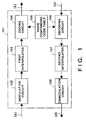
- FIG. 1 is a schematic block diagram showing the construction of a digital modem (codec/modem) 101 according to a first embodiment.
- FIG. 8 is a schematic block diagram showing the construction of a facsimile according to the first embodiment.
- the D/A and A/D converters in the modem and the D/A and A/D converters in the voice codec are removed from the conventional modem/voice codec processing basic composition shown in FIG. 10, the LPF in the modem and the LPF in the voice codec, which are unnecessary due to the removal of the above converters, are also taken away, and interpolaters 103 and 107 are substituted for the converters and the LPFs.
- a digital transmit signal (a) input to a modulation circuit 102 is modulated by a carrier frequency prescribed according to the CCITT Recommendation.
- the modulated output signal is a digital signal, and output in each sampling clock which is normally 9.6KHz.
- the output signal is input to a first interpolater 103 and sampled by a sampling clock of 8.0KHz. In other words, the sampling conversion from 9.6KHz to 8.0KHz is carried out.
- the converted signal is furthermore input to a coding circuit 104, converted to an audio PCM transmission code (b) with reference to a voice companding code table 105, and output in a sampling clock of 8.0KHz.
- An input audio PCM receive code (c) is decoded by a decoding circuit 106 with reference to the voice companding code table 105.
- the decoded digital signal is output in the sampling clock of 8.0KHz.
- the output signal is input to a second interpolater 107 and sampled by a sampling clock which is normally 9.6KHz.
- the converted signal is furthermore demodulated by a demodulation circuit 108 and output as a digital receive signal (d) in a sampling clock of 9.6KHz.
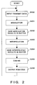
- Step S202 the six modulation results are temporarily saved in an unillustrated buffer in preparation for the subsequent interpolation.
- Step S203 the interpolation using the saved six data is performed by the first interpolater 103, the conversion of the sampling frequency from 9.6KHz to 8.0KHz is achieved.
- Step S204 the interpolation results are temporarily saved in Step S204 in preparation for the subsequent PCM coding.
- the coding circuit 104 performs coding according to G. 711 of the CCITT Recommendation in Step S205, and a PCM code is output in Step S206.
- Steps S200 to S206 are repeated in each symbol interval (1/1600").
- FIG. 4 shows a discrete modulation waveform obtained by the process in Step S201 shown in FIG. 2, and a dotted line expresses an envelope.
- the five data arranged at regular intervals are obtained by calculating values of an envelope at intervals of 1/8000".
- Step S300 the decoding circuit 106 decodes the input five PCM codes according to G. 711 of the CCITT Recommendation in Step S301. Then, in Step S302, the decoded results are temporarily saved in preparation for the subsequent interpolation.
- Step S303 interpolation using the saved five data is executed by the second interpolater 107 in Step S303, and the sampling frequency conversion from 8.0KHz to 9.6KHz is achieved.
- Step S304 the interpolation results are temporarily saved in Step S304 in preparation for the subsequent demodulation.
- FIG. 6 shows a discrete receive waveform obtained by the process in Step S301 shown in FIG. 3, and a dotted line expresses an envelope.
- the envelope expressed in the dotted line can be formed by interpolation based on the five data.
- the six data arranged at regular intervals are obtained by calculating values of the envelope at intervals of 1/9600".
- the following effects can be obtained by digitally performing the modem/PCM codec processing.
- the A/D and D/A converters mounted in the modem which normally operate at a sample rate of 9.6KHz and the A/D and D/A converters mounted in the PCM codec which normally operate at a sample rate of 8.0KHz are taken away from the conventional communication control unit, the LPF in the modem and the LPF in the PCM codec are also taken away, and a sample rate conversion processing circuit is disposed between the modem and the PCM codec instead of the above converters and the LPFs. It is thereby possible to digitally achieve the modem modulation/demodulation processing and the PCM codec processing, and thus to reduce the quantitizing errors.
- the size of the circuit is made small and costs are lowered.
- a digital modem 101 having a simple structure and capable of preventing quantitizing errors by digitally executing the modem modulation/demodulation and the voice codec processing.
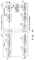
- FIG. 11 is a schematic block diagram showing the construction of a digital modem 101 according to the second embodiment.
- FIG. 12 is a schematic block diagram showing the construction of a facsimile according to the second embodiment.
- the D/A and A/D converters in the modem and the D/A and A/D converters in the voice codec are removed from the conventional modem/voice codec processing basic composition shown in FIG. 10, the LPF in the modem and the LPF in the voice codec, which are unnecessary due to the removal of the above converters, are also taken away, and interpolaters 103 and 107 are substituted for the converters and LPFs.
- Either ⁇ -law or A-law can be selected by a control line (e) as a PCM coding rule which is referred to in coding and decoding.
- a digital transmit signal (a) input to a modulation circuit 102 is modulated by a carrier frequency prescribed according to the CCITT Recommendation.
- the modulated output signal is a digital signal, and output in each sampling clock which is normally 9.6KHz.
- the output signal is input to a first interpolater 103 and sampled by a sampling clock of 8.0KHz. In other words, the sampling conversion from 9.6KHz to 8.0KHz is carried out.
- the converted signal is furthermore input to a coding circuit 104, converted to an audio PCM transmission code (b) with reference to a memory 105a in which an A-law voice companding/expanded code table is stored or a memory 105b in which a ⁇ -law voice companding/expanded code table is stored, either which is selected beforehand by an interlock switch SW, and output.
- a coding circuit 104 converted to an audio PCM transmission code (b) with reference to a memory 105a in which an A-law voice companding/expanded code table is stored or a memory 105b in which a ⁇ -law voice companding/expanded code table is stored, either which is selected beforehand by an interlock switch SW, and output.
- An input audio PCM receive signal (c) is decoded by a decoding circuit 106 with reference to either the A-law voice companding/expanded code table 105a or the ⁇ -law voice companding/expanded code table 105b which is selected by the interlock switch SW.
- the decoded digital signal is output in a sampling clock of 8.0KHz.
- the output signal is input to a second interpolater 107 and sampled by a sampling clock which is normally 9.6KHz.
- the sampling conversion from 8.0KHz to 9.6KHz is carried out.
- the converted signal is furthermore demodulated by a demodulation circuit 108 and output as a digital receive signal (d).
- PCM coding rule is selected according to the control from the facsimile control portion 814 in the above embodiment, it is also possible to select the PCM coding rule by another method, for example, by turning on and off a bit switch disposed in the communication control unit.
- the modem modulation/demodulation and the voice codec processing can be digitally processed and a PCM coding rule to be referred to in coding and decoding can be selected, it is possible to simplify the structure of the digital modem 101 , to prevent quantitizing errors, and to enhance the convenience of the digital modem 101.
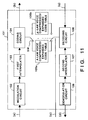
- FIG. 13 is a schematic block diagram showing the construction of a digital modem 101 according to the third embodiment.
- FIG. 14 is a schematic block diagram showing the construction of a facsimile according to the third embodiment.
- the D/A and A/D converters in the modem and the D/A and A/D converters in the voice codec are removed from the conventional modem/voice codec processing basic composition shown in FIG. 10, the LPF in the modem and the LPF in the voice codec, which are unnecessary due to the removal of the above converters, are also taken away, and interpolaters 103 and 107 are substituted for the converters and the LPFs.
- a switch SW1 is disposed between the output of the modulator and the input of the demodulator, a switch SW2 is disposed between the output of the first interpolater and the input of the second interpolater, and a switch SW3 is disposed between the output of the coding circuit and the input of the decoding circuit.
- the switches SW1 to SW3 shown in FIG. 13 are controlled by the facsimile control portion 814.
- Transmitting and receiving operations in the above construction are the same as those in the above first embodiment, and therefore, the description of the operations is omitted.
- Step S401 data generated inside the modulation circuit 102 or transmit data from the FAX is modulated by the modulation circuit 102.
- the modulated data is demodulated by the demodulation circuit 108 in Step S402, thereby restoring the transmit data. It is checked by the facsimile control portion 814 in Step S403 whether or not the transmitted data and the restored data are the same, and the check result is output to an display 820 and the like. Then, it is determined by the facsimile control portion 814 in Step S404 whether or not the above process is executed a predetermined number of times. If the process is not executed a predetermined number of times, Step S401 is executed again and the above checking operations are repeated.
- Data generated inside the modulation circuit 102 or transmit data from the facsimile cntrol portion 814 is modulated by the modulation circuit 102 in Step S501.
- Interpolation is performed by the first interpolater 103 in Step S502, and the sampling frequency conversion from 9.6KHz to 8.0KHz is executed.
- interpolation is performed by the second interpolater 107 in Step S503, and the sampling frequency conversion from 8.0KHz to 9.6KHz is executed in preparation for subsequent demodulation.
- Step S504 the transmit data is demodulated by the demodulation circuit 108 based on data whose sampling frequency is returned to 9.6KHz. It is checked by the facsimile control portion 814 in Step S505 whether or not the transmitted data and the restored data are the same. As a result, if no error is found, it is possible to determine that the modulation, the demodulation and the first and second interpolations are normally executed. In Step S506, it is determined whether by the facsimile control portion 814 or not a series of processes are performed a predetermined number of times. If the processes are not performed a predetermined number of times, Step S501 is executed again and the above processes are repeated.
- Data generated inside the modulation circuit 102 or transmit data from the facsimile control portion 814 is modulated by the modulation circuit 102 in Step S601.
- Interpolation is performed by the first interpolater 103 in Step S602, and the sampling frequency conversion from 9.6KHz to 8.0KHz is carried out.
- Step S603 coding is performed by the coding circuit 104 so as to convert the modulated data to a PCM transmission code.
- the PCM transmission code is decoded by the decoding circuit 106 in Step S604.
- Step S605 interpolation is performed by the second interpolater 107 so that the decoded data can be demodulated. In other words, the sampling frequency conversion from 8.0KHz to 9.6KHz is carried out.
- the interpolation result is demodulated by the demodulation circuit 108 in Step S606, and the transmitted data is restored.
- the restored transmit data is compared with actually transmit data by the facsimile control portion 814 in Step S607 and it is checked whether or not both the data are the same. As a result, if no error is found, it is possible to determine that the modulation, the demodulation, the first and second interpolations, the coding and the decoding are normally executed.
- Step S608 it is determined by the facsimile control portion 814 whether or not the above series of processes are performed a predetermined number of times. If the processes are not performed a predetermined number of times, Step S601 is executed again and the above processes are repeated.
- Self-checking of the transmission processing system such as modulation and demodulation processing and PCM/voice codec processing, is made possible by mounting a plurality of paths for short-circuiting transmitting and receiving paths (loopback function), and thus, it is possible to easily determine a part where a failure occurred.
- the modem modulation and demodulation and the voice codec processing can be digitally carried out and a part of the transmission processing system where a failure occurred can be easily determined, it is possible to simplify the structure of the digital modem 101 , to prevent quantitizing errors, and to enhance the convenience of the digital modem 101 .
- sampling frequencies for modulation/demodulation and for the PCM codec processing are set at 9.6KHz and 8.0KHz, respectively, the sampling frequencies of the present invention are not limited to these values.
- interpolation of the present invention is not limited to the above interpolating methods.
- the present invention is applicable to a modulating device without any demodulating function and a demodulating device without any modulating function, besides a modem having both modulating and demodulating functions.
- the present invention is also applicable to a simple coding circuit and a simple decoding circuit.
- a digital communication device of the present invention is provided with a modulation circuit for modulating a digital transmit signal, a first interpolater for converting the modulated signal in frequency, a coding circuit for coding the signal converted in frequency into an audio PCM transmission code with reference to a voice companding code table, a decoding circuit for decoding a coded audio PCM receive code into a digital signal with reference to the voice companding code table, a second interpolater for converting the decoded digital signal in frequency, and a demodulation circuit for demodulating the converted signal, and digitally performs modem modulation/demodulation and voice codec processing.
Abstract
Description
- The present invention relates to a digital communication device for communicating a modulated signal through a digital line.
- A typical digital modem for performing modem/voice codec processes is mounted in a communication control unit for a facsimile having G3/G4 functions connected to a digital line. The communication control unit of the G3/G4 facsimile is constructed as shown in FIG. 9. Referring to FIG.9,
numeral 817 denotes a processing section having G3/G4 functions. On the other hand,numeral 801 denotes a communication control section. - In this example, an Integrated Services Digital Network (ISDN) is used as a digital line, and a part corresponding to the subscriber's line is, herein, expressed as a S interface.
- A facsimile communication operation of the communication control unit according to the prior art will now be described.
- First, the case in which the communication control unit functions as a G4 facsimile will be explained. In this case, it is assumed that switches SW1 and SW2 shown in FIG. 9 each are connected (turned ON) to the side of G4.
- In the
above processing section 817, afacsimile control portion 814 executes various kinds of control operations in order to make the whole unit function as a facsimile. Thefacsimile control portion 814 operates anetwork control portion 813 and carries out a call-out procedure or a call-in procedure by using aG4 terminal number 816, previous to facsimile transmission. In the ISDN, these procedures are carried out by using a D channel, and thus thenetwork control portion 813 is connected to the S interface through a Dchannel control circuit 808 and aline interface circuit 802. After the connection of the unit to the network is thus completed, facsimile transmission is started. - The
facsimile control portion 814 carries out a procedure b 812 previous to image transmission. Theprocedure b 812 is a G4 communication procedure according to T. 62, T. 73 and T. 70 of the CCITT Recommendation. - These procedures are connected to the switch SW1 through a
connecting circuit 807. The connectingcircuit 807 is a connecting circuit for digital communication according to X. 21bis of the CCITT Recommendation. These procedures and the image transmission are normally executed by using a B channel in the ISDN, and thus the connectingcircuit 807 is connected to the S interface through a Bchannel control circuit 803 and theline interface circuit 802. - Subsequently, when the connection is completed, the
facsimile control portion 814 operates aMMR codec 811, thereby starting to transmit image data. TheMMR codec 811 executes coding and decoding of image data according to T. 6 of the CCITT Recommendation, and compresses and expands the data. - A codec for executing coding/decoding processes according to T. 6 will be referred to as a Modified Modified READ (MMR) codec hereinafter. The image data is also generally transmitted by using the B channel in the ISDN, and thus the
MMR codec 811 is connected to the S interface through theconnecting circuit 807, the B-channel control circuit 803 and theline interface circuit 802. - Image transmission with the G4 facsimile function is carried out according to the above-mentioned operations.
- The case in which the communication control unit functions as a G3 facsimile will now be described. In this case, it is assumed that the switches SW1 and SW2 shown in FIG. 9 are connected (turned ON) to G3.
- First, the
facsimile control portion 814 operates thenetwork control portion 813 and carries out a call-out procedure or a call-in procedure by using aG3 phone number 815, previous to facsimile transmission. The G3phone number 815 is actually the number of a digital telephone. When the procedures are completed through thenetwork control portion 813, the D-channel control circuit 808 and theline interface circuit 802, a line of audio communication between a terminal of the subscriber and the other terminal is established. - Although not shown in FIG. 9, a voice call by a digital telephone through the B channel is possible in this state.
- After the connection of the the terminal of the subscriber to the network and the other terminal is established, facsimile transmission is started.
- The
facsimile control portion 814 operates a procedure a 810 previous to image transmission. The procedure a 810 is a G3 and G2 communication control procedure according to T. 30 of the CCITT Recommendation. This communication procedure is carried out by analog signals (in the voice grade) through amodem 805. In the case of a conventional G3 facsimile, since its communication line is an analog line, communication is possible in this state. - However, in the ISDN, the analog signals are converted into digital signals through a
voice codec 806 for a digital telephone, and audio communication is performed through the B-channel control circuit 803 and theline interface circuit 802. Themodem 805 is a modem (V21) for a communication control procedure according to the CCITT Recommendation. - After carrying out the communication procedure with the other terminal, the
facsimile control portion 814 operates a MH/MR codec 809 so as to start image transmission. The MH/MR codec 809 performs a G3 coding/decoding processes of image data according to T. 4 of the CCITT Recommendation and compresses and expands the image data. - The image data is converted into analog signals (in the voice grade) through the
modem 805. Themodem 805 is a modem (V27ter or V29) for G3 image transmission according to the CCITT Recommendation. These image signals are also connected to the S interface through thevoice codec 806, the B-channel control circuit 803 and theline interface circuit 802 in the same manner as above. - Image transmission with the G3 facsimile function is performed according to the above-mentioned operations.
- The components (the
modem 805 and the voice codec 806) enclosed by theline 804 shown in FIG. 9 will now be described in detail with reference to FIG. 10. - The
modem 805 performs modulation or demodulation on the basis of a digital operation, and executes D/A or A/D conversion in each sampling clock which is normally 9.6KHz. Thevoice codec 806 is an audio PCM codec for converting analog signals in the voice grade into digital signals and performing compression coding, or performing the operations in reverse order, and generally executes A/D or D/A conversion and corresponding coding/decoding in each sampling clock which is 8.0KHz. - In transmission, a digital transmit signal (a) is input to a
modulation circuit 901, and modulated by a carrier frequency prescribed in the CCITT Recommendation. The digital output signal from themodulation circuit 901 is converted into an analog transmit signal (b) in the voice grade by a first D/A converter 902 and a first lowpass filter (LPF) 903. The signal (b) is input to thevoice codec 806, and converted into a digital signal again by a first A/D converter 904, and furthermore, coded into an audio PCM transmission code (c) by acoding circuit 905 with reference to a voice companding code table 906 and output. - The
first lowpass filter 903 and asecond lowpass filter 909 remove harmonic noise included in analog signals output from the first D/A converter 902 and a second D/A converter 908. - Receiving operations will now be described.
- As illustrated, an audio PCM receive code (d) is input to a
decoding circuit 907 and decoded with reference to the voice companding code table 906. The decoded digital signal is converted into an analog signal (e) in the voice grade by the second D/A converter 908 and thesecond LPF 909. The analog signal (e) is input to a second A/D converter 910 in themodem 805 and converted into a digital signal again. Then, the digital signal is demodulated and output as a digital receive signal (f) by ademodulation circuit 911. - However, in the above prior art shown in FIG. 10, since the sampling frequency of the D/A and A/
D converters modem 805 and the sampling frequency of the A/D and D/A converters voice codec 806 are different, the conversion, a digital signal ' an analog signal ' a digital signal, is necessary between themodem 805 and thevoice codec 806, thereby causing a quantitizing error which results in the deteriorated transmission ability. - Since both sampling frequencies of 9.6KHz and 8.0KHz are used, the
modem 805 and thevoice codec 806 constitutes an extremely large circuitry. It is necessary to design a LSI for themodem 805 and a LSI for thevoice codec 806 as separate chips. This needs a wide space and increases costs. - Furthermore, since either of functions µ-law or A-law is only used as a PCM coding rule which is referred to in coding and decoding, it is necessary to prepare a codec according to the PCM coding rule used in an area where a data communication apparatus is installed. If the data communication apparatus is transferred to an area where a different PCM coding rule is used, inconveniently, it is necessary to replace the codec.
- In addition, since a transmission processing system, such as modulation, demodulation and PCM/voice codec processing, cannot be checked for itself, it is not possible to easily determine a part of the transmission system where a failure occurred.
- The present invention aims to solve the above problems. Therefore, an object of the present invention is to provide a digital communication device capable of digitally processing modem modulation and demodulation and voice codec processes.
- Another object of the present invention is to provide a codec capable of selecting a PCM coding rule to be referred to in coding and decoding.
- A further object of the present invention is to provide a modem capable of easily determining a part of a transmission processing system where a failure occurred.
- Additional and other objects of the present invention will become apparent from the detailed description in conjunction with the accompanying drawings.
-
- FIG. 1 is a schematic block diagram showing the construction of a
digital modem 101 according to a first embodiment; - FIG. 2 is a flowchart showing operations of a transmitting side in the embodiment;
- FIG. 3 is a flowchart showing operations of a receiving side in the embodiment;
- FIGS. 4 and 5 are views explaining processing of a first interpolater;
- FIGS. 6 and 7 are views explaining processing of a second interpolater;
- FIG. 8 is a schematic block diagram showing the construction of a facsimile according to the first embodiment;
- FIG. 9 is a schematic block diagram showing the construction of a communication control unit for a conventional facsimile;
- FIG. 10 is a detailed block diagram showing the constructions of a modem and a voice codec shown in FIG. 9;
- FIG. 11 is a schematic block diagram showing the construction of a
digital modem 101 according to a second embodiment; - FIG. 12 is a schematic block diagram showing the construction of a facsimile according to the second embodiment;
- FIG. 13 is a schematic block diagram showing the construction of a
digital modem 101 according to a third embodiment; - FIG. 14 is a schematic block diagram showing the construction of a facsimile according to the third embodiment; and
- FIGS. 15 to 17 are flowcharts showing the procedures for loopback tests in the third embodiment.
-
- A preferred embodiment of the present invention will now be described in detail with reference to the accompanying drawings.
- FIG. 1 is a schematic block diagram showing the construction of a digital modem (codec/modem) 101 according to a first embodiment.
- FIG. 8 is a schematic block diagram showing the construction of a facsimile according to the first embodiment.
- As illustrated, in this embodiment, the D/A and A/D converters in the modem and the D/A and A/D converters in the voice codec are removed from the conventional modem/voice codec processing basic composition shown in FIG. 10, the LPF in the modem and the LPF in the voice codec, which are unnecessary due to the removal of the above converters, are also taken away, and interpolaters 103 and 107 are substituted for the converters and the LPFs.
- In the above construction, when a transmission operation is performed, a digital transmit signal (a) input to a
modulation circuit 102 is modulated by a carrier frequency prescribed according to the CCITT Recommendation. The modulated output signal is a digital signal, and output in each sampling clock which is normally 9.6KHz. The output signal is input to afirst interpolater 103 and sampled by a sampling clock of 8.0KHz. In other words, the sampling conversion from 9.6KHz to 8.0KHz is carried out. The converted signal is furthermore input to acoding circuit 104, converted to an audio PCM transmission code (b) with reference to a voice companding code table 105, and output in a sampling clock of 8.0KHz. - A receiving operation will now be described.
- An input audio PCM receive code (c) is decoded by a
decoding circuit 106 with reference to the voice companding code table 105. The decoded digital signal is output in the sampling clock of 8.0KHz. Then, the output signal is input to asecond interpolater 107 and sampled by a sampling clock which is normally 9.6KHz. In other words, the sampling conversion from 8.0KHz to 9.6KHz is carried out. The converted signal is furthermore demodulated by ademodulation circuit 108 and output as a digital receive signal (d) in a sampling clock of 9.6KHz. - Operations of a transmitting side of the
digital modem 101 according this embodiment will be described with reference to the flowchart shown in FIG. 2. - The case that a V27ter modem is used and the transmission rate is 4800bps is given as an example.
- The
modulation circuit 102 shown in FIG. 1 repeats processes in each transmit data symbol (1/1600"). Therefore, one transmit data symbol (= 3 bit) is read from a transmitting facsimile (FAX) in Step S200 shown in FIG.2, and demodulation for a symbol cycle (1/1600") is conducted on the data by a basic frequency having a cycle of 1/9600" in Step S201. In other words, six (= 1/1600 ÷ 1/9600) modulation results can be obtained by executing processing by the basic frequency having a cycle of 1/9600" for 1/1600" - In Step S202, the six modulation results are temporarily saved in an unillustrated buffer in preparation for the subsequent interpolation. Then, in Step S203, the interpolation using the saved six data is performed by the
first interpolater 103, the conversion of the sampling frequency from 9.6KHz to 8.0KHz is achieved. This sampling frequency conversion can be performed by conducting interpolation by using the six data in a symbol interval ( = 1/1600"), obtaining five interpolation results, and sampling the results at regular intervals (1/8000 = 1/1600 ÷ 5). - When the above interpolation is completed, the interpolation results are temporarily saved in Step S204 in preparation for the subsequent PCM coding. The
coding circuit 104 performs coding according to G. 711 of the CCITT Recommendation in Step S205, and a PCM code is output in Step S206. - The above-mentioned processes in Steps S200 to S206 are repeated in each symbol interval (1/1600").
- The above interpolation will now be described in detail with reference to FIGS. 4 and 5.
- FIG. 4 shows a discrete modulation waveform obtained by the process in Step S201 shown in FIG. 2, and a dotted line expresses an envelope. As shown in FIG. 4, six discrete data are arranged at regular intervals (= 1/9600") in a symbol interval (= 1/1600"), and the envelope expressed in the dotted line can be formed by performing interpolation processing based on the six data.
- FIG. 5 shows that five discrete data are arranged at regular intervals (= 1/8000") in a symbol interval (= 1/1600") after the sampling frequency conversion from 9.6KHz to 8.0KHz. The five data arranged at regular intervals are obtained by calculating values of an envelope at intervals of 1/8000".
- Operations of a receiving side of the
digital modem 101 in this embodiment will now be described with reference to the flowchart shown in FIG. 3. - The processes are repeated in each receive data symbol (1/1600 ") on the receiving side in the same manner as in the transmitting side. Therefore, one receive data symbol, that is, five PCM codes (= 1/1600 ÷ 1/8000) are input in Step S300 shown in FIG. 3. Subsequently, the
decoding circuit 106 decodes the input five PCM codes according to G. 711 of the CCITT Recommendation in Step S301. Then, in Step S302, the decoded results are temporarily saved in preparation for the subsequent interpolation. - Next, interpolation using the saved five data is executed by the
second interpolater 107 in Step S303, and the sampling frequency conversion from 8.0KHz to 9.6KHz is achieved. This sampling conversion can be carried out by performing interpolation based on the five data in the symbol interval (= 1/1600"), obtaining six interpolation results, and sampling the results at regular intervals (1/1600 ÷ 6 = 1/9600). - When the above interpolation is completed, the interpolation results are temporarily saved in Step S304 in preparation for the subsequent demodulation. In Step S305, the six interpolation results are demodulated by the
demodulation circuit 108 in a symbol cycle (1/1600") by a basic frequency having a cycle of 1/9600". Then, one symbol data (= 3 bit) is obtained as a result and output to the FAX in Step S306. - The above interpolation on the receiving side will be explained with reference to FIGS. 6 and 7.
- FIG. 6 shows a discrete receive waveform obtained by the process in Step S301 shown in FIG. 3, and a dotted line expresses an envelope. As shown in FIG. 6, five discrete data are arranged at regular intervals (= 1/8000") in a symbol interval (= 1/1600"). The envelope expressed in the dotted line can be formed by interpolation based on the five data.
- FIG. 7 shows that six discrete data are arranged at regular intervals (= 1/9600") in a symbol interval (= 1/1600") after the sampling frequency conversion from 8.0KHz to 9.6KHz. The six data arranged at regular intervals are obtained by calculating values of the envelope at intervals of 1/9600".
- As described above, according to this embodiment, the following effects can be obtained by digitally performing the modem/PCM codec processing.
- The A/D and D/A converters mounted in the modem which normally operate at a sample rate of 9.6KHz and the A/D and D/A converters mounted in the PCM codec which normally operate at a sample rate of 8.0KHz are taken away from the conventional communication control unit, the LPF in the modem and the LPF in the PCM codec are also taken away, and a sample rate conversion processing circuit is disposed between the modem and the PCM codec instead of the above converters and the LPFs. It is thereby possible to digitally achieve the modem modulation/demodulation processing and the PCM codec processing, and thus to reduce the quantitizing errors.
- Furthermore, since two sets of A/D and D/A converters and two LPFs can be removed, the size of the circuit is made small and costs are lowered. In addition, it is easy to merge the modem and the PCM codec into a chip instead of the conventional composition of the modem, the PCM code, and the LSIs, and thus it can be greatly expected to save the space.
- As described above, according to this embodiment, it is possible to provide a
digital modem 101 having a simple structure and capable of preventing quantitizing errors by digitally executing the modem modulation/demodulation and the voice codec processing. - A second embodiment of the present invention will now be described with reference to the accompanying drawings.
- FIG. 11 is a schematic block diagram showing the construction of a
digital modem 101 according to the second embodiment. - FIG. 12 is a schematic block diagram showing the construction of a facsimile according to the second embodiment.
- As illustrated, in this embodiment, the D/A and A/D converters in the modem and the D/A and A/D converters in the voice codec are removed from the conventional modem/voice codec processing basic composition shown in FIG. 10, the LPF in the modem and the LPF in the voice codec, which are unnecessary due to the removal of the above converters, are also taken away, and interpolaters 103 and 107 are substituted for the converters and LPFs. Either µ-law or A-law can be selected by a control line (e) as a PCM coding rule which is referred to in coding and decoding.
- In the above construction, when a transmission operation is performed, a digital transmit signal (a) input to a
modulation circuit 102 is modulated by a carrier frequency prescribed according to the CCITT Recommendation. The modulated output signal is a digital signal, and output in each sampling clock which is normally 9.6KHz. The output signal is input to afirst interpolater 103 and sampled by a sampling clock of 8.0KHz. In other words, the sampling conversion from 9.6KHz to 8.0KHz is carried out. The converted signal is furthermore input to acoding circuit 104, converted to an audio PCM transmission code (b) with reference to amemory 105a in which an A-law voice companding/expanded code table is stored or amemory 105b in which a µ-law voice companding/expanded code table is stored, either which is selected beforehand by an interlock switch SW, and output. - A receiving operation will now be described.
- An input audio PCM receive signal (c) is decoded by a
decoding circuit 106 with reference to either the A-law voice companding/expanded code table 105a or the µ-law voice companding/expanded code table 105b which is selected by the interlock switch SW. The decoded digital signal is output in a sampling clock of 8.0KHz. Then, the output signal is input to asecond interpolater 107 and sampled by a sampling clock which is normally 9.6KHz. - In other words, the sampling conversion from 8.0KHz to 9.6KHz is carried out. The converted signal is furthermore demodulated by a
demodulation circuit 108 and output as a digital receive signal (d). - Therefore, it is possible to cope with both A-law and µ-law by allowing the PCM coding rule to be selected by the interlock switch SW.
- Although the PCM coding rule is selected according to the control from the
facsimile control portion 814 in the above embodiment, it is also possible to select the PCM coding rule by another method, for example, by turning on and off a bit switch disposed in the communication control unit. - As described above, according to this embodiment, since the modem modulation/demodulation and the voice codec processing can be digitally processed and a PCM coding rule to be referred to in coding and decoding can be selected, it is possible to simplify the structure of the
digital modem 101 , to prevent quantitizing errors, and to enhance the convenience of thedigital modem 101. - A third embodiment of the present invention will be described with reference to the drawings.
- FIG. 13 is a schematic block diagram showing the construction of a
digital modem 101 according to the third embodiment. - FIG. 14 is a schematic block diagram showing the construction of a facsimile according to the third embodiment.
- As illustrated, in this embodiment, the D/A and A/D converters in the modem and the D/A and A/D converters in the voice codec are removed from the conventional modem/voice codec processing basic composition shown in FIG. 10, the LPF in the modem and the LPF in the voice codec, which are unnecessary due to the removal of the above converters, are also taken away, and interpolaters 103 and 107 are substituted for the converters and the LPFs. Furthermore, a switch SW1 is disposed between the output of the modulator and the input of the demodulator, a switch SW2 is disposed between the output of the first interpolater and the input of the second interpolater, and a switch SW3 is disposed between the output of the coding circuit and the input of the decoding circuit.
- The switches SW1 to SW3 shown in FIG. 13 are controlled by the
facsimile control portion 814. - Transmitting and receiving operations in the above construction are the same as those in the above first embodiment, and therefore, the description of the operations is omitted.
- All of the above switches SW1 to SW3 are in the off state.
- The procedures for loopback tests which are made by short-circuiting by the above switches paths for transmission and receiving of the
digital modem 101 in this embodiment will now be described. - First, a loopback test on the
modulation circuit 102 and thedemodulation circuit 108 shown in FIG. 13 will be explained according to the flowchart shown in FIG. 15. - In this case, it is assumed that only the switch SW1 is on and the other switches SW2 and SW3 are off.
- In Step S401, data generated inside the
modulation circuit 102 or transmit data from the FAX is modulated by themodulation circuit 102. The modulated data is demodulated by thedemodulation circuit 108 in Step S402, thereby restoring the transmit data. It is checked by thefacsimile control portion 814 in Step S403 whether or not the transmitted data and the restored data are the same, and the check result is output to an display 820 and the like. Then, it is determined by thefacsimile control portion 814 in Step S404 whether or not the above process is executed a predetermined number of times. If the process is not executed a predetermined number of times, Step S401 is executed again and the above checking operations are repeated. - According to the above process, if no error is found in the above step S403, it is possible to determine that modulation and demodulation are normally performed.
- A loopback test on the
modulation circuit 102, thefirst interpolater 103, thesecond interpolater 107 and thedemodulation circuit 108 will now be described according to the flowchart shown in FIG. 16. - In this case, it is assumed that only the switch SW2 is on and the other switches SW1 and SW3 are off.
- Data generated inside the
modulation circuit 102 or transmit data from thefacsimile cntrol portion 814 is modulated by themodulation circuit 102 in Step S501. Interpolation is performed by thefirst interpolater 103 in Step S502, and the sampling frequency conversion from 9.6KHz to 8.0KHz is executed. Then, interpolation is performed by thesecond interpolater 107 in Step S503, and the sampling frequency conversion from 8.0KHz to 9.6KHz is executed in preparation for subsequent demodulation. - In Step S504, the transmit data is demodulated by the
demodulation circuit 108 based on data whose sampling frequency is returned to 9.6KHz. It is checked by thefacsimile control portion 814 in Step S505 whether or not the transmitted data and the restored data are the same. As a result, if no error is found, it is possible to determine that the modulation, the demodulation and the first and second interpolations are normally executed. In Step S506, it is determined whether by thefacsimile control portion 814 or not a series of processes are performed a predetermined number of times. If the processes are not performed a predetermined number of times, Step S501 is executed again and the above processes are repeated. - Finally, a loopback test on the whole transmission processing system in this embodiment will be described according to the flowchart shown in FIG. 17.
- In this case, it is assumed that only the switch SW3 is on and the other switches SW1 and SW2 are off.
- Data generated inside the
modulation circuit 102 or transmit data from thefacsimile control portion 814 is modulated by themodulation circuit 102 in Step S601. Interpolation is performed by thefirst interpolater 103 in Step S602, and the sampling frequency conversion from 9.6KHz to 8.0KHz is carried out. In Step S603, coding is performed by thecoding circuit 104 so as to convert the modulated data to a PCM transmission code. The PCM transmission code is decoded by thedecoding circuit 106 in Step S604. In Step S605, interpolation is performed by thesecond interpolater 107 so that the decoded data can be demodulated. In other words, the sampling frequency conversion from 8.0KHz to 9.6KHz is carried out. - The interpolation result is demodulated by the
demodulation circuit 108 in Step S606, and the transmitted data is restored. The restored transmit data is compared with actually transmit data by thefacsimile control portion 814 in Step S607 and it is checked whether or not both the data are the same. As a result, if no error is found, it is possible to determine that the modulation, the demodulation, the first and second interpolations, the coding and the decoding are normally executed. - In Step S608, it is determined by the
facsimile control portion 814 whether or not the above series of processes are performed a predetermined number of times. If the processes are not performed a predetermined number of times, Step S601 is executed again and the above processes are repeated. - As described above, it is possible to easily determine a part of the
digital modem 101 where a failure occurred by executing the loopback tests according to FIGS. 15 to 17 in this order. In other words, for example, if thedigital modem 101 passes the loopback tests according to FIGS. 15 and 16 and does not pass the loopback test according to FIG. 17, it is possible to assume that a failure occurred in thePCM coding circuit 104 or thePCM decoding circuit 106. - Self-checking of the transmission processing system, such as modulation and demodulation processing and PCM/voice codec processing, is made possible by mounting a plurality of paths for short-circuiting transmitting and receiving paths (loopback function), and thus, it is possible to easily determine a part where a failure occurred.
- As described above, according to this embodiment, since the modem modulation and demodulation and the voice codec processing can be digitally carried out and a part of the transmission processing system where a failure occurred can be easily determined, it is possible to simplify the structure of the
digital modem 101 , to prevent quantitizing errors, and to enhance the convenience of thedigital modem 101 . -
- Although the sampling frequencies for modulation/demodulation and for the PCM codec processing are set at 9.6KHz and 8.0KHz, respectively, the sampling frequencies of the present invention are not limited to these values.
- Furthermore, although the case in which a V27ter modem is used and the transmission rate is 4800bps is described, it is obvious that the present invention can be easily applied to other modems.
- Although a simple interpolation is performed as sampling frequency conversion, the same effect can be obtained even by using splined interpolation, interpolation with a polynomial, or the like. The interpolation of the present invention is not limited to the above interpolating methods.
- In addition, although the description is given with a consciousness that the sampling frequency conversion is realized by DSP, the realization of the conversion in the present invention is not limited to the realization by hardware and software.
- The present invention is applicable to a modulating device without any demodulating function and a demodulating device without any modulating function, besides a modem having both modulating and demodulating functions.
- The present invention is also applicable to a simple coding circuit and a simple decoding circuit.
- While the present invention is described in conjunction with preferred embodiments, it will be apparent that the present invention is not limited to the above-mentioned embodiments and that various changes and modifications thereof can be made without departing from the spirit and scope of the invention as defined in the appended claims.
- A digital communication device of the present invention is provided with a modulation circuit for modulating a digital transmit signal, a first interpolater for converting the modulated signal in frequency, a coding circuit for coding the signal converted in frequency into an audio PCM transmission code with reference to a voice companding code table, a decoding circuit for decoding a coded audio PCM receive code into a digital signal with reference to the voice companding code table, a second interpolater for converting the decoded digital signal in frequency, and a demodulation circuit for demodulating the converted signal, and digitally performs modem modulation/demodulation and voice codec processing.
Claims (16)
- A modulation device for outputting digital data modulated in accordance with a carrier frequency to a coding circuit, comprising:
first conversion means for converting input signals into first digital signals modulated in accordance with a carrier frequency; and
second conversion means for converting said first digital signals input at first intervals into second digital signals input at second intervals different from said first intervals. - A modulation device according to claim 1, wherein said first conversion means sequentially converts said input signals input at the predetermined intervals into said first digital signals modulated in accordance with the carrier frequency.
- A modulation device according to claim 1, wherein said second conversion means converts said first digital signals input at said first intervals into said second digital signals at said second intervals by interpolation.
- A modulation device according to claim 1, wherein said second intervals are equal to intervals between sampling clocks of said coding circuit.
- A modulation device according to claim 1, wherein said first intervals are shorter than said second intervals.
- A demodulation device for demodulating data decoded by a decoding circuit, comprising:
conversion means for converting decoded data input at first intervals into data at second intervals different from said first intervals; and
processing means for performing demodulation based on said data at said second intervals which are converted by said conversion means. - A demodulation device according to claim 6, wherein said first intervals are equal to intervals between sampling clocks of said decoding circuit.
- A demodulation device according to claim 6, wherein said conversion means converts said decoded data input at said first intervals into said data at said second intervals by interpolation.
- A demodulation device according to claim 6, wherein said second intervals are shorter than said first intervals.
- A digital communication device connected to a digital network for performing modem and voice codec processing, comprising:
modulation means for modulating a digital signal;
first conversion means for converting the signal modulated by said modulation means in frequency;
coding means for coding the signal converted by said first conversion means;
decoding means for decoding the signal coded by said coding means;
second conversion means for converting the signal decoded by said decoding means in frequency; and
demodulation means for demodulating the signal converted by said second conversion means. - A digital communication device according to claim 10, wherein said first conversion means performs the frequency conversion by outputting the signal, which is input from said modulation means in each first sampling clock, in each second sampling clock.
- A digital communication device according to claim 10, wherein said second conversion means performs the frequency conversion by outputting the signal, which is input from said decoding means in each of said sampling clock, in each of said first sampling clock.
- A processing device, comprising:
memory means for storing first and second PCM coding rules referred to in coding or decoding; and
selection means for selecting either of said first and second PCM coding rules stored by said memory means,
wherein the coding or decoding is carried out with reference to said PCM coding rule selected by said selection means. - A processing device according to claim 13, wherein said selection means selects either of said first and second PCM coding rules by a switch.
- A digital communication device for performing modem and voice codec processing, having a plurality of short-circuit means for short-circuiting a transmission path and a receive path and capable of determining a part of a transmission processing system where a failure occurred in accordance with the path short-circuited by said short-circuit means.
- A digital communication device according to claim 15, further comprising:
comparing means for comparing a signal from the path short-circuited by said short-circuit means and an initial signal; and
determining means for determining the part of said transmission processing means where a failure occurred based on the result of the comparison by said comparing means.
Applications Claiming Priority (6)
| Application Number | Priority Date | Filing Date | Title |
|---|---|---|---|
| JP2224342A JP2972300B2 (en) | 1990-08-28 | 1990-08-28 | Communication device |
| JP224342/90 | 1990-08-28 | ||
| JP226519/90 | 1990-08-30 | ||
| JP2226518A JP2922606B2 (en) | 1990-08-30 | 1990-08-30 | Communication device |
| JP2226519A JP2866170B2 (en) | 1990-08-30 | 1990-08-30 | Communication device |
| JP226518/90 | 1990-08-30 |
Publications (3)
| Publication Number | Publication Date |
|---|---|
| EP0473116A2 true EP0473116A2 (en) | 1992-03-04 |
| EP0473116A3 EP0473116A3 (en) | 1993-02-24 |
| EP0473116B1 EP0473116B1 (en) | 1999-04-07 |
Family
ID=27330884
Family Applications (1)
| Application Number | Title | Priority Date | Filing Date |
|---|---|---|---|
| EP91114366A Expired - Lifetime EP0473116B1 (en) | 1990-08-28 | 1991-08-27 | Digital communication device |
Country Status (3)
| Country | Link |
|---|---|
| US (1) | US5818870A (en) |
| EP (1) | EP0473116B1 (en) |
| DE (1) | DE69131087T2 (en) |
Cited By (22)
| Publication number | Priority date | Publication date | Assignee | Title |
|---|---|---|---|---|
| EP0651542A2 (en) * | 1993-10-27 | 1995-05-03 | Canon Kabushiki Kaisha | Digital telephone overcoming incompatibilities in international digital telephone standards |
| FR2721469A1 (en) * | 1994-06-20 | 1995-12-22 | Siemens Ag | Method and device for transmitting audio signals between communication terminals. |
| WO1996018261A2 (en) * | 1994-12-09 | 1996-06-13 | Brent Townshend | High speed communications system for analog subscriber connections |
| US6111935A (en) * | 1993-10-27 | 2000-08-29 | Canon Kabushiki Kaisha | Adaptive expansion table in a digital telephone receiver |
| US6341360B1 (en) | 1999-03-08 | 2002-01-22 | International Business Machines Corporation | Decision feedback equalizers, methods, and computer program products for detecting severe error events and preserving equalizer filter characteristics in response thereto |
| US6381267B1 (en) | 1999-03-08 | 2002-04-30 | International Business Machines Corporation | Modems, methods, and computer program products for falling back to a lower data rate protocol upon detecting abnormal line conditions during startup |
| US6389064B1 (en) | 1999-03-08 | 2002-05-14 | International Business Machines Corporation | Modems, methods, and computer program products for identifying a signaling alphabet in variance with an ideal alphabet due to digital impairments |
| US6400770B1 (en) | 1994-12-09 | 2002-06-04 | Brent Townshend | High speed encoding and decoding methods for analog subscriber connections |
| US6553518B1 (en) | 1999-03-08 | 2003-04-22 | International Business Machines Corporation | Severe error detectors, methods and computer program products that use constellation specific error event thresholds to detect severe error events during demodulation of a signal comprising symbols from a plurality of symbol constellations |
| US6611563B1 (en) | 1999-10-29 | 2003-08-26 | International Business Machines Corporation | Systems, methods and computer program products for data mode refinement of modem constellation points |
| US6650657B1 (en) | 1999-10-29 | 2003-11-18 | International Business Machines Corporation | Systems, methods and computer program products for identifying digital impairments in modem signals |
| US6661847B1 (en) | 1999-05-20 | 2003-12-09 | International Business Machines Corporation | Systems methods and computer program products for generating and optimizing signal constellations |
| US6661837B1 (en) | 1999-03-08 | 2003-12-09 | International Business Machines Corporation | Modems, methods, and computer program products for selecting an optimum data rate using error signals representing the difference between the output of an equalizer and the output of a slicer or detector |
| US6662322B1 (en) | 1999-10-29 | 2003-12-09 | International Business Machines Corporation | Systems, methods, and computer program products for controlling the error rate in a communication device by adjusting the distance between signal constellation points |
| US6754258B1 (en) | 1999-10-29 | 2004-06-22 | International Business Machines Corporation | Systems, methods and computer program products for averaging learned levels in the presence of digital impairments based on patterns |
| US6765955B1 (en) | 1999-10-29 | 2004-07-20 | International Business Machines Corporation | Methods, systems and computer program products establishing a communication configuration for a modem connection to compensate for echo noise |
| US6792040B1 (en) | 1999-10-29 | 2004-09-14 | International Business Machines Corporation | Modems having a dual power mode capability and methods of operating same |
| US6816545B1 (en) | 1999-10-29 | 2004-11-09 | International Business Machines Corporation | Systems, methods and computer program products for identifying digital impairments in modems based on clusters and/or skips in pulse code modulation signal levels |
| US6823017B1 (en) | 1999-10-29 | 2004-11-23 | International Business Machines Corporation | Systems, methods and computer program products for filtering glitches from measured values in a sequence of code points |
| US6823004B1 (en) | 1999-10-29 | 2004-11-23 | International Business Machines Corporation | Methods, systems and computer program products for monitoring performance of a modem during a connection |
| US6826157B1 (en) | 1999-10-29 | 2004-11-30 | International Business Machines Corporation | Systems, methods, and computer program products for controlling data rate reductions in a communication device by using a plurality of filters to detect short-term bursts of errors and long-term sustainable errors |
| US7003030B2 (en) | 1999-03-08 | 2006-02-21 | Lenovo (Singapore) Pte. Ltd. | Receivers, methods, and computer program products for an analog modem that receives data signals from a digital modem |
Families Citing this family (14)
| Publication number | Priority date | Publication date | Assignee | Title |
|---|---|---|---|---|
| US6449352B1 (en) * | 1995-06-20 | 2002-09-10 | Matsushita Electric Industrial Co., Ltd. | Packet generating method, data multiplexing method using the same, and apparatus for coding and decoding of the transmission data |
| US5991278A (en) * | 1996-08-13 | 1999-11-23 | Telogy Networks, Inc. | Asymmetric modem communications system and method |
| US6212228B1 (en) * | 1997-09-10 | 2001-04-03 | Nortel Networks Limited | Apparatus for modulation and demodulating digital data |
| TW522354B (en) * | 1998-08-31 | 2003-03-01 | Semiconductor Energy Lab | Display device and method of driving the same |
| US6504865B1 (en) * | 1999-02-24 | 2003-01-07 | Altocom, Inc. | Digital connection detection technique |
| US6397276B1 (en) | 1999-03-29 | 2002-05-28 | Eugene Rzyski | Data transmission by an alternating-frequency analog signal |
| US6504866B1 (en) * | 1999-05-14 | 2003-01-07 | Siemens Information & Communication Networks, Inc | System and method for eliminating companding conversion distortion on international modem calls |
| US6505222B1 (en) | 1999-10-29 | 2003-01-07 | International Business Machines Corporation | Systems methods and computer program products for controlling undesirable bias in an equalizer |
| US6876339B2 (en) | 1999-12-27 | 2005-04-05 | Semiconductor Energy Laboratory Co., Ltd. | Semiconductor device and driving method thereof |
| JP2001186360A (en) * | 1999-12-27 | 2001-07-06 | Canon Inc | Picture communication equipment and its method |
| EP1594269B1 (en) * | 2000-05-17 | 2008-06-18 | Symstream Technology Holdings No. 2 PTY LTD | Octave pulse data encoding and decoding method and apparatus |
| JP2005079929A (en) * | 2003-09-01 | 2005-03-24 | Canon Inc | Communication apparatus, control method of communication apparatus, and control program for communication apparatus |
| US8135362B2 (en) | 2005-03-07 | 2012-03-13 | Symstream Technology Holdings Pty Ltd | Symbol stream virtual radio organism method and apparatus |
| JP4371150B2 (en) * | 2007-05-14 | 2009-11-25 | セイコーエプソン株式会社 | Facsimile apparatus, control method thereof, and program |
Citations (5)
| Publication number | Priority date | Publication date | Assignee | Title |
|---|---|---|---|---|
| GB2200510A (en) * | 1986-12-09 | 1988-08-03 | Hitachi Ltd | Facsimile communication system |
| US4771335A (en) * | 1985-08-26 | 1988-09-13 | Kabushiki Kaisha Toshiba | Method and apparatus for sending data |
| US4837812A (en) * | 1985-12-21 | 1989-06-06 | Ricoh Company, Ltd. | Dual connection mode equipped communication control apparatus |
| JPH01144762A (en) * | 1987-11-30 | 1989-06-07 | Canon Inc | Line control equipment |
| US4860115A (en) * | 1987-05-09 | 1989-08-22 | Ricoh Company, Ltd. | Digital copier with a facsimile function |
Family Cites Families (18)
| Publication number | Priority date | Publication date | Assignee | Title |
|---|---|---|---|---|
| US4035724A (en) * | 1974-05-08 | 1977-07-12 | Universite De Sherbrooke | Digital converter from continuous variable slope delta modulation to pulse code modulation |
| US4044306A (en) * | 1974-07-26 | 1977-08-23 | Universite De Snerbrooke | Digital converter from pulse code modulation to continuous variable slope delta modulation |
| NL176211C (en) * | 1974-09-16 | 1985-03-01 | Philips Nv | INTERPOLING DIGITAL FILTER. |
| NL168669C (en) * | 1974-09-16 | 1982-04-16 | Philips Nv | INTERPOLING DIGITAL FILTER WITH INPUT BUFFER. |
| US4021616A (en) * | 1976-01-08 | 1977-05-03 | Ncr Corporation | Interpolating rate multiplier |
| NL173339C (en) * | 1978-11-30 | 1984-01-02 | Philips Nv | DIGITAL-ANALOGUE CONVERTER. |
| NL8202319A (en) * | 1982-06-09 | 1984-01-02 | Philips Nv | TRANSMISSION SYSTEM FOR THE TRANSFER OF TWO-VALUE DATA SYMBOLS. |
| EP0113514B1 (en) * | 1982-11-30 | 1988-05-11 | BRITISH TELECOMMUNICATIONS public limited company | Television signal transmission |
| NL8400676A (en) * | 1984-03-02 | 1985-10-01 | Philips Nv | DATA TRANSMISSION SYSTEM. |
| NL8400677A (en) * | 1984-03-02 | 1985-10-01 | Philips Nv | TRANSMISSION SYSTEM FOR THE TRANSMISSION OF DATA SIGNALS IN A MODULAR TIRE. |
| US4700226A (en) * | 1986-10-17 | 1987-10-13 | Rca Corporation | Rate buffer control of predicted signal decimation and interpolation for adaptive differential pulse code modulator |
| JPH0693667B2 (en) * | 1988-08-03 | 1994-11-16 | 富士通株式会社 | Synchronous multiplexing |
| DE68908149T2 (en) * | 1989-01-10 | 1994-03-17 | Ibm | Modem with software-adjusted keying speed. |
| US5136618A (en) * | 1989-01-19 | 1992-08-04 | Redband Technologies, Inc. | Method and apparatus for bandwidth reduction of modulated signals |
| US5148167A (en) * | 1990-04-06 | 1992-09-15 | General Electric Company | Sigma-delta oversampled analog-to-digital converter network with chopper stabilization |
| US5199046A (en) * | 1991-09-09 | 1993-03-30 | Codex Corporation | First and second digital rate converter synchronization device and method |
| GB2267192B (en) * | 1992-05-21 | 1995-09-27 | Sony Broadcast & Communication | Sampling frequency conversion |
| DE4308617A1 (en) * | 1993-03-18 | 1994-09-22 | Thomson Brandt Gmbh | Digital recording and playback device |
-
1991
- 1991-08-22 US US07/748,527 patent/US5818870A/en not_active Expired - Fee Related
- 1991-08-27 EP EP91114366A patent/EP0473116B1/en not_active Expired - Lifetime
- 1991-08-27 DE DE69131087T patent/DE69131087T2/en not_active Expired - Fee Related
Patent Citations (5)
| Publication number | Priority date | Publication date | Assignee | Title |
|---|---|---|---|---|
| US4771335A (en) * | 1985-08-26 | 1988-09-13 | Kabushiki Kaisha Toshiba | Method and apparatus for sending data |
| US4837812A (en) * | 1985-12-21 | 1989-06-06 | Ricoh Company, Ltd. | Dual connection mode equipped communication control apparatus |
| GB2200510A (en) * | 1986-12-09 | 1988-08-03 | Hitachi Ltd | Facsimile communication system |
| US4860115A (en) * | 1987-05-09 | 1989-08-22 | Ricoh Company, Ltd. | Digital copier with a facsimile function |
| JPH01144762A (en) * | 1987-11-30 | 1989-06-07 | Canon Inc | Line control equipment |
Non-Patent Citations (2)
| Title |
|---|
| PATENT ABSTRACTS OF JAPAN, vol. 13, no. 404 (E-817), 7th September 1989; & JP-A-1 144 762 (CANON INC.) 07-06-1989 * |
| Schönfelder, "Digitale Filter in der Videotechnik", Drei-R-Verlag, Berlin 1988, pages 121 to 124 * |
Cited By (33)
| Publication number | Priority date | Publication date | Assignee | Title |
|---|---|---|---|---|
| US6111935A (en) * | 1993-10-27 | 2000-08-29 | Canon Kabushiki Kaisha | Adaptive expansion table in a digital telephone receiver |
| EP0651542A3 (en) * | 1993-10-27 | 1995-10-18 | Canon Kk | Digital telephone overcoming incompatibilities in international digital telephone standards. |
| EP0651542A2 (en) * | 1993-10-27 | 1995-05-03 | Canon Kabushiki Kaisha | Digital telephone overcoming incompatibilities in international digital telephone standards |
| US5652782A (en) * | 1993-10-27 | 1997-07-29 | Canon Inc. | Digital telephone overcoming international incompatibilities |
| FR2721469A1 (en) * | 1994-06-20 | 1995-12-22 | Siemens Ag | Method and device for transmitting audio signals between communication terminals. |
| US6233324B1 (en) | 1994-06-20 | 2001-05-15 | Siemens Aktiengesellschaft | Method and arrangement for transmitting audio signals between communication terminal equipment |
| US6690749B2 (en) | 1994-12-09 | 2004-02-10 | Brent Townshend | High speed encoding and decoding apparatus and method for analog subscriber connections |
| US5809075A (en) * | 1994-12-09 | 1998-09-15 | Townshend; Brent | High speed communications system for analog subscriber connections |
| US5835538A (en) * | 1994-12-09 | 1998-11-10 | Townshend; Brent | High speed communications system for analog subscriber connections |
| AU701274B2 (en) * | 1994-12-09 | 1999-01-21 | Brent Townshend | High speed communications system for analog subscriber connections |
| AU708086B2 (en) * | 1994-12-09 | 1999-07-29 | Brent Townshend | High speed encoder and encoding method |
| AU708085B2 (en) * | 1994-12-09 | 1999-07-29 | Brent Townshend | High speed data transfer system and method |
| US5801695A (en) * | 1994-12-09 | 1998-09-01 | Townshend; Brent | High speed communications system for analog subscriber connections |
| WO1996018261A3 (en) * | 1994-12-09 | 1996-08-29 | Brent Townshend | High speed communications system for analog subscriber connections |
| WO1996018261A2 (en) * | 1994-12-09 | 1996-06-13 | Brent Townshend | High speed communications system for analog subscriber connections |
| US6400770B1 (en) | 1994-12-09 | 2002-06-04 | Brent Townshend | High speed encoding and decoding methods for analog subscriber connections |
| US6389064B1 (en) | 1999-03-08 | 2002-05-14 | International Business Machines Corporation | Modems, methods, and computer program products for identifying a signaling alphabet in variance with an ideal alphabet due to digital impairments |
| US6381267B1 (en) | 1999-03-08 | 2002-04-30 | International Business Machines Corporation | Modems, methods, and computer program products for falling back to a lower data rate protocol upon detecting abnormal line conditions during startup |
| US6553518B1 (en) | 1999-03-08 | 2003-04-22 | International Business Machines Corporation | Severe error detectors, methods and computer program products that use constellation specific error event thresholds to detect severe error events during demodulation of a signal comprising symbols from a plurality of symbol constellations |
| US6341360B1 (en) | 1999-03-08 | 2002-01-22 | International Business Machines Corporation | Decision feedback equalizers, methods, and computer program products for detecting severe error events and preserving equalizer filter characteristics in response thereto |
| US7003030B2 (en) | 1999-03-08 | 2006-02-21 | Lenovo (Singapore) Pte. Ltd. | Receivers, methods, and computer program products for an analog modem that receives data signals from a digital modem |
| US6661837B1 (en) | 1999-03-08 | 2003-12-09 | International Business Machines Corporation | Modems, methods, and computer program products for selecting an optimum data rate using error signals representing the difference between the output of an equalizer and the output of a slicer or detector |
| US6661847B1 (en) | 1999-05-20 | 2003-12-09 | International Business Machines Corporation | Systems methods and computer program products for generating and optimizing signal constellations |
| US6611563B1 (en) | 1999-10-29 | 2003-08-26 | International Business Machines Corporation | Systems, methods and computer program products for data mode refinement of modem constellation points |
| US6662322B1 (en) | 1999-10-29 | 2003-12-09 | International Business Machines Corporation | Systems, methods, and computer program products for controlling the error rate in a communication device by adjusting the distance between signal constellation points |
| US6754258B1 (en) | 1999-10-29 | 2004-06-22 | International Business Machines Corporation | Systems, methods and computer program products for averaging learned levels in the presence of digital impairments based on patterns |
| US6765955B1 (en) | 1999-10-29 | 2004-07-20 | International Business Machines Corporation | Methods, systems and computer program products establishing a communication configuration for a modem connection to compensate for echo noise |
| US6792040B1 (en) | 1999-10-29 | 2004-09-14 | International Business Machines Corporation | Modems having a dual power mode capability and methods of operating same |
| US6816545B1 (en) | 1999-10-29 | 2004-11-09 | International Business Machines Corporation | Systems, methods and computer program products for identifying digital impairments in modems based on clusters and/or skips in pulse code modulation signal levels |
| US6823017B1 (en) | 1999-10-29 | 2004-11-23 | International Business Machines Corporation | Systems, methods and computer program products for filtering glitches from measured values in a sequence of code points |
| US6823004B1 (en) | 1999-10-29 | 2004-11-23 | International Business Machines Corporation | Methods, systems and computer program products for monitoring performance of a modem during a connection |
| US6826157B1 (en) | 1999-10-29 | 2004-11-30 | International Business Machines Corporation | Systems, methods, and computer program products for controlling data rate reductions in a communication device by using a plurality of filters to detect short-term bursts of errors and long-term sustainable errors |
| US6650657B1 (en) | 1999-10-29 | 2003-11-18 | International Business Machines Corporation | Systems, methods and computer program products for identifying digital impairments in modem signals |
Also Published As
| Publication number | Publication date |
|---|---|
| US5818870A (en) | 1998-10-06 |
| EP0473116A3 (en) | 1993-02-24 |
| EP0473116B1 (en) | 1999-04-07 |
| DE69131087T2 (en) | 1999-10-28 |
| DE69131087D1 (en) | 1999-05-12 |
Similar Documents
| Publication | Publication Date | Title |
|---|---|---|
| US5818870A (en) | Digital communication device | |
| US5142568A (en) | Data communication apparatus which can use either an analog or a digital line | |
| US5970128A (en) | Telephone device for caller identification | |
| US5090052A (en) | Telephone system with multiple extension telephones | |
| US5995558A (en) | Rob bit compensation system and method associated with a receiver or codec | |
| EP0216488B1 (en) | Digital signal processor | |
| US4884285A (en) | (DS) transmitter | |
| US5189525A (en) | Facsimile apparatus | |
| US5588052A (en) | DTMF signal judging apparatus | |
| US6178186B1 (en) | Fractional decimator with linear interpolation and method thereof | |
| US6574012B1 (en) | Communication terminal apparatus of determining a communication speed for line condition | |
| EP0514076B1 (en) | Communication apparatus for connection to a public switched telephone network | |
| US6052409A (en) | Device and method for generating and detecting tones in a digital data communications device | |
| JP2866170B2 (en) | Communication device | |
| JP2922606B2 (en) | Communication device | |
| JP2972300B2 (en) | Communication device | |
| JP3216319B2 (en) | Digital audio transmitting device, receiving device, and transmitting / receiving device | |
| JP2538148B2 (en) | Fax modem | |
| JP2793807B2 (en) | Image communication device | |
| JPH01177727A (en) | Picture communication equipment | |
| CA1111582A (en) | Signal processor for use with a telephone system and a digital transmission system | |
| JPS6025348A (en) | Data transmission system | |
| JPH082071B2 (en) | Signaling transmission method | |
| JPH09275456A (en) | Facsimile equipment | |
| JPH0793660B2 (en) | Data communication device |
Legal Events
| Date | Code | Title | Description |
|---|---|---|---|
| PUAI | Public reference made under article 153(3) epc to a published international application that has entered the european phase |
Free format text: ORIGINAL CODE: 0009012 |
|
| AK | Designated contracting states |
Kind code of ref document: A2 Designated state(s): DE FR GB |
|
| PUAL | Search report despatched |
Free format text: ORIGINAL CODE: 0009013 |
|
| AK | Designated contracting states |
Kind code of ref document: A3 Designated state(s): DE FR GB |
|
| 17P | Request for examination filed |
Effective date: 19930712 |
|
| 17Q | First examination report despatched |
Effective date: 19950607 |
|
| APAB | Appeal dossier modified |
Free format text: ORIGINAL CODE: EPIDOS NOAPE |
|
| APAB | Appeal dossier modified |
Free format text: ORIGINAL CODE: EPIDOS NOAPE |
|
| APAD | Appeal reference recorded |
Free format text: ORIGINAL CODE: EPIDOS REFNE |
|
| APAB | Appeal dossier modified |
Free format text: ORIGINAL CODE: EPIDOS NOAPE |
|
| GRAG | Despatch of communication of intention to grant |
Free format text: ORIGINAL CODE: EPIDOS AGRA |
|
| GRAH | Despatch of communication of intention to grant a patent |
Free format text: ORIGINAL CODE: EPIDOS IGRA |
|
| GRAH | Despatch of communication of intention to grant a patent |
Free format text: ORIGINAL CODE: EPIDOS IGRA |
|
| GRAA | (expected) grant |
Free format text: ORIGINAL CODE: 0009210 |
|
| AK | Designated contracting states |
Kind code of ref document: B1 Designated state(s): DE FR GB |
|
| REF | Corresponds to: |
Ref document number: 69131087 Country of ref document: DE Date of ref document: 19990512 |
|
| ET | Fr: translation filed | ||
| PLBE | No opposition filed within time limit |
Free format text: ORIGINAL CODE: 0009261 |
|
| STAA | Information on the status of an ep patent application or granted ep patent |
Free format text: STATUS: NO OPPOSITION FILED WITHIN TIME LIMIT |
|
| 26N | No opposition filed | ||
| REG | Reference to a national code |
Ref country code: GB Ref legal event code: IF02 |
|
| PGFP | Annual fee paid to national office [announced via postgrant information from national office to epo] |
Ref country code: FR Payment date: 20040810 Year of fee payment: 14 |
|
| PGFP | Annual fee paid to national office [announced via postgrant information from national office to epo] |
Ref country code: GB Payment date: 20040825 Year of fee payment: 14 |
|
| PGFP | Annual fee paid to national office [announced via postgrant information from national office to epo] |
Ref country code: DE Payment date: 20040902 Year of fee payment: 14 |
|
| PG25 | Lapsed in a contracting state [announced via postgrant information from national office to epo] |
Ref country code: GB Free format text: LAPSE BECAUSE OF NON-PAYMENT OF DUE FEES Effective date: 20050827 |
|
| APAH | Appeal reference modified |
Free format text: ORIGINAL CODE: EPIDOSCREFNO |
|
| PG25 | Lapsed in a contracting state [announced via postgrant information from national office to epo] |
Ref country code: DE Free format text: LAPSE BECAUSE OF NON-PAYMENT OF DUE FEES Effective date: 20060301 |
|
| GBPC | Gb: european patent ceased through non-payment of renewal fee |
Effective date: 20050827 |
|
| PG25 | Lapsed in a contracting state [announced via postgrant information from national office to epo] |
Ref country code: FR Free format text: LAPSE BECAUSE OF NON-PAYMENT OF DUE FEES Effective date: 20060428 |
|
| REG | Reference to a national code |
Ref country code: FR Ref legal event code: ST Effective date: 20060428 |