EP0464223A1 - Weight measuring apparatus - Google Patents
Weight measuring apparatus Download PDFInfo
- Publication number
- EP0464223A1 EP0464223A1 EP91902779A EP91902779A EP0464223A1 EP 0464223 A1 EP0464223 A1 EP 0464223A1 EP 91902779 A EP91902779 A EP 91902779A EP 91902779 A EP91902779 A EP 91902779A EP 0464223 A1 EP0464223 A1 EP 0464223A1
- Authority
- EP
- European Patent Office
- Prior art keywords
- digital
- signal
- input
- analog
- output
- Prior art date
- Legal status (The legal status is an assumption and is not a legal conclusion. Google has not performed a legal analysis and makes no representation as to the accuracy of the status listed.)
- Granted
Links
Images

Classifications
-
- G—PHYSICS
- G01—MEASURING; TESTING
- G01G—WEIGHING
- G01G3/00—Weighing apparatus characterised by the use of elastically-deformable members, e.g. spring balances
- G01G3/12—Weighing apparatus characterised by the use of elastically-deformable members, e.g. spring balances wherein the weighing element is in the form of a solid body stressed by pressure or tension during weighing
- G01G3/14—Weighing apparatus characterised by the use of elastically-deformable members, e.g. spring balances wherein the weighing element is in the form of a solid body stressed by pressure or tension during weighing measuring variations of electrical resistance
- G01G3/142—Circuits specially adapted therefor
- G01G3/147—Circuits specially adapted therefor involving digital counting
-
- G—PHYSICS
- G01—MEASURING; TESTING
- G01G—WEIGHING
- G01G23/00—Auxiliary devices for weighing apparatus
- G01G23/18—Indicating devices, e.g. for remote indication; Recording devices; Scales, e.g. graduated
- G01G23/36—Indicating the weight by electrical means, e.g. using photoelectric cells
- G01G23/37—Indicating the weight by electrical means, e.g. using photoelectric cells involving digital counting
- G01G23/3707—Indicating the weight by electrical means, e.g. using photoelectric cells involving digital counting using a microprocessor
- G01G23/3714—Indicating the weight by electrical means, e.g. using photoelectric cells involving digital counting using a microprocessor with feedback means
-
- G—PHYSICS
- G01—MEASURING; TESTING
- G01G—WEIGHING
- G01G23/00—Auxiliary devices for weighing apparatus
- G01G23/48—Temperature-compensating arrangements
-
- G—PHYSICS
- G01—MEASURING; TESTING
- G01G—WEIGHING
- G01G3/00—Weighing apparatus characterised by the use of elastically-deformable members, e.g. spring balances
- G01G3/12—Weighing apparatus characterised by the use of elastically-deformable members, e.g. spring balances wherein the weighing element is in the form of a solid body stressed by pressure or tension during weighing
- G01G3/14—Weighing apparatus characterised by the use of elastically-deformable members, e.g. spring balances wherein the weighing element is in the form of a solid body stressed by pressure or tension during weighing measuring variations of electrical resistance
- G01G3/142—Circuits specially adapted therefor
-
- G—PHYSICS
- G01—MEASURING; TESTING
- G01G—WEIGHING
- G01G3/00—Weighing apparatus characterised by the use of elastically-deformable members, e.g. spring balances
- G01G3/18—Temperature-compensating arrangements
Definitions
- the present invention relates to a weight measuring apparatus which is arranged such that analog signals from different lines are input thereto through a plurality of channels. More particularly, the present invention relates to a weight measuring apparatus which is designed so that various measuring error factors included in an analog signal from each line, e.g., a drift in an analog signal processing circuit, a zero point change of the load cell output, etc., are removed by a digital signal processing means that executes a real-time filtering processing.
- various measuring error factors included in an analog signal from each line e.g., a drift in an analog signal processing circuit, a zero point change of the load cell output, etc.
- a post-stage digital signal processing system comprises a single line
- an analog signal processing system which is previous to it comprises a plurality of lines
- an analog filter is used in each line.
- the circuit is complicated, the number of parts increases, and mounting of circuit elements becomes troublesome.
- analog filters since analog filters are used, each filter must be switched over to a buffer in the drift compensation mode, so that the circuit becomes complicated further correspondingly.
- the filter constant must be varied in accordance with the installation environment, replacement of a circuit element that determines the filter constant is also troublesome.
- the above-mentioned invention (2) needs in the temperature detection mode to pass a signal from a temperature sensor through a filter for a weight signal which differs therefrom in frequency characteristics and hence it involves a slight lag in the signal processing.
- the signal processing system comprises a single line
- the signal processing lag can be ignored to a certain extent.
- the signal processing system comprises a plurality of lines
- the lag cannot be ignored.
- the invention (2) cannot be applied to a weighing apparatus which needs to execute sequential processing of analog signals from a plurality of lines.
- the present invention aims at solving the above-described problems, and it is an object of the present invention to provide a weight measuring apparatus which is designed so that, even if the analog signal processing system comprises a plurality of lines, signal processing can be effected at high speed as if the system were comprised of a single line and that it is also possible to compensate for a drift that occurs in each analog signal processing system, a zero point change of the load cell output due to temperature, and so forth.
- the weight measuring apparatus of the present invention comprises input signal switching means for selectively outputting analog signals input to a plurality of channels, analog-to-digital converter means (hereinafter referred to as “A/D converter means”) for converting an analog signal output from the input signal switching means into a digital signal, and digital signal processing means (hereinafter referred to as "DSP”) for filtering a digital quantity output from the analog-to-digital converter means for each channel, or filtering digital quantities from a plurality of channels after these digital quantities have been combined together.
- A/D converter means analog-to-digital converter means
- DSP digital signal processing means
- the weight measuring apparatus is a weight checker that comprises a weighting conveyor and a plurality of load cells that support it
- analog signals from various channels that are input to the input signal switching means are defined as output signals from the corresponding load cells.
- the load cell outputs are sequentially input to the A/D converter means by a channel switching operation.
- the DSP filters a digital quantity in each channel that is output from the A/D converter means for each channel and outputs the filtered digital quantity to a microcomputer.
- the microcomputer adds together the digital quantities from the various channels to determine a weight value. Alternatively, the digital quantities are added together directly in the DSP to determine a weight value without supplying them to the microcomputer.
- the load cell outputs are sequentially input to the DSP at a sampling period that is determined by the A/D converter means.
- filtering for each channel is sequentially executed with a time lag involved in the digital conversion. Accordingly, filtering for each channel can be regared as progressing in parallel and substantially simultaneously considering the time cycle required for weighing. As a result, even in a weighing apparatus that needs to input sequentially analog signals from different lines through a plurality of channels, signal processing can be executed at high speed as if the apparatus were comprised of a single line.
- an analog signal that is input to one channel is defined as a reference voltage signal
- the DSP obtains a drift from a temporal change of the reference voltage signal.
- the DSP then subtracts the drift from the digital quantity of a weight signal input thereto from the same analog signal processing system. More specifically, if there are analog signal processing systems for a plurality of channels, a drift is obtained for each channel, and it is subtracted from the digital quantity in the corresponding channel.
- the digital quantity of the reference voltage signal is used as it is or after being filtered to obtain a drift, and the drift thus obtained is subtracted from the digital quantity of the filtered weight signal.
- the drift is subtracted from the digital quantity of the weight signal before filtering, and the result of the subtraction is filtered to obtain a weight value.
- the drift in each channel is subtracted from the sum of the digital quantities before filtering and the result of the subtraction is then filtered.
- the drift in each channel is subtracted from the filtered sum.
- analog signals that are input to half the number of channels at the most are output signals each from a temperature sensor that detects the temperature of the corresponding load cell, and the DSP outputs the output signal from the temperature sensor to the microcomputer as it is or after it has been filtered.
- the microcomputer deduces a load cell temperature at that time from the output temperature characteristics of the temperature sensor already stored on the basis of the temperature detecting signal and calculates a zero point change of the load cell output at the temperature concerned from the deduced temperature and the output temperature characteristics of the load cell output. Then, the zero point change is transferred to and stored in the DSP.
- Such processing may also be executed in the DSP, as a matter of course.
- the microcomputer or the DSP subtracts the stored zero point change from the digital quantity corresponding to the output signal of the load cell.
- the zero point change may be subtracted from the filtered digital quantity, or filtering may be effected after the subtraction. Since such temperature compensation needs to be made for each load cell, each of the load cells is designated at a proper timing to obtain a zero point change in advance.
- the zero point change in each channel is subtracted from the sum of the digital quantities before filtering, and the result of the subtraction is then filtered.
- the sum of the digital quantities is first filtered and the zero point change in each channel is then subtracted from the filtered sum.
- the above-described temperature compensation and drift compensation together by a similar channel switching operation regardless of whether the system comprises a single load cell or a plurality of load cells.
- a single load cell a three-channel input signal switching means is used, and a weight signal from the load cell is input to one of the three channels, a reference voltage signal to another channel, and a detection signal from a temperature sensor to the other channel.
- Fig. 1 is a side view of a weighting section of a weight checker
- Fig. 2 is a front view of the weighing section.
- a weighing conveyor A is supported by a pair of front and rear load cells L each disposed in a direction perpendicular to the direction of movement of the conveyor A.
- Rubber vibration isolators D are interposed between the weighing conveyor A and the load cells L to absorb horizontal stress that is induced in the load cells L by the deflection of the weighing conveyor A.
- the weighing conveyor A comprises a pair of front and rear rollers 1 and 2, which are attached to frames F, a flat belt 3 that is stretched between the rollers 1 and 2, a top plate 4 that is disposed underneath the upper running section of the flat belt 3, a motor 5 that is attached to the frames F under the top plate 4, a pulley 6 that is secured to a driving shaft of the motor 5, a pulley 7 that is secured to a rotating shaft of one roller 1, and a toothed belt 8 that is stretched between the two pulleys 6 and 7.
- Each load cell L which is of the parallel beam type, is attached at one end (fixed end) thereof to a base B and has a bracket E attached to the other end (movable end) thereof, thereby supporting the weighing conveyor A.
- the number of load cells may be varied according to need.
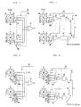
- Figs. 3 and 4 are block diagrams each showing a signal processing circuit of the weight checker in which the weighing conveyor A is supported by a plurality of load cells L.
- the signal processing circuit shown in Fig. 3 is arranged such that output signals S1 to Sn from the load cells L are input directly to a multiplexer 10 that functions as an input signal switching means.
- the signal processing circuit shown in Fig. 4 is arranged such that the output signals S1 to Sn from the load cells L are input to the multiplexer 10 through respective operational amplifiers 11.
- the analog signals S1 to Sn that are input to the multiplexer 10 are selected in response to a channel switching signal Sc from a microcomputer 17 and output to an operational amplifier 11.
- the operational amplifier 11 amplifies the input analog signal with a predetermined amplification factor and outputs the amplified analog signal to an anti-alias filter 13 through a level shift circuit 12.
- the output signals S1 to Sn from the load cells are amplified in the respective operational amplifiers 11 before being input to the multiplexer 10 through the respective level shift circuits 12.
- one of the signals S1 to Sn is selected and input to an anti-alias filter 13 in response to a channel switching signal Sc from a microcomputer 17.
- the level shift circuits 12 are provided to match the dynamic range of the analog signals S1 to Sn with the input range of an A/D converter means 14.
- the level shift circuit 12 in Fig. 3 comprises an adder that adds together an output voltage from a digital-to-analog converter 15 and an output voltage from the operational amplifier 11, whereas each level shift circuit 12 in Fig. 4 comprises a bias circuit.
- the anti-alias filter 13 comprises an analog filter that passes only a signal in a frequency band that satisfies a sampling theorem, thereby preventing a return phenomenon which would otherwise be caused by a signal in a frequency band above 1/2 of the sampling frequency that is determined by the A/D converter means 14.
- the A/D converter means 14 which comprises a successive comparison type A/D converter, is arranged such that its A/D converting operation and a filtering operation by a DSP (Digital signal Processor) 16 are synchronized with each other by a synchronizing signal Ss that is output from the DSP 16.
- DSP Digital signal Processor
- the digital-to-analog converter 15 operates such that analog signal levels whose initial values vary from each other are adjusted to substantially the same level.
- the digital-to-analog converter 15 is instructed by the microcomputer 12 to output a voltage for shifting a signal level in a designated channel to a predetermined level. Accordingly, in a case where the output levels of the analog signals S1 to Sn are substantially equal to each other, the digital-to-analog converter 15 may be omitted. In such a case, the level shift circuit comprises a mere bias circuit.
- the DSP 16 effects filtering by a numerical calculation, as is generally known, and has an FIR (Finite Impulse Response) type low-pass filter which has been programmed therein.
- FIR Finite Impulse Response
- the DSP 16 executes filtering regarding the channel concerned and also executes a predetermined processing programmed, thereby calculating a weight value. This processing will be described later.
- reference numeral 18 denotes an input means for inputting various kinds of data
- 19 a display means.
- Figs. 5 and 6 are diagrams each showing one example of a circuit disposed in a stage which is previous to the multiplexer 10 shown in Fig. 3.
- the circuit is arranged as shown in Fig. 5
- load cell temperature compensation is to be made
- the circuit is arranged as shown in Fig. 6.
- drift compensation and load cell temperature compensation are to be made together, these circuit configurations are combined together.
- each bridge circuit 20 comprises four strain gages 21, which are provided for each of the load cells L, and output terminals of each bridge circuit 20 are connected to one of the input channels C1...Cn-1 of the multiplexer 10. Since in Fig. 3 a drift occurs in a common analog signal processing circuit, one output terminal of one bridge circuit 20 is further branched to define reference voltage signal terminals, which are connected to one input channel Cn of the multiplexer 10, as shown in Fig. 5.
- temperature detecting circuits 22 are attached to the bridge circuits 20, respectively, and output terminals of the detecting circuits 22 are connected to input channels of the multiplexer 10, as shown in Fig. 6.
- Figs. 7 and 8 are diagrams each showing one example of a circuit disposed in a stage which is previous to the multiplexer 10 shown in Fig. 4.
- the circuit is arranged as shown in Fig. 7
- load cell temperature compensation is to be made
- the circuit is arranged as shown in Fig. 8.
- drift compensation and load cell temperature compensation are to be made together, these circuit configurations are combined together.
- a signal switching circuit 23 is provided in a stage which is previous to each operational amplifier 11 to selectively output a weight signal and a reference voltage signal by its signal switching operation. More specifically, each signal switching circuit 23 is normally connected to a contact a, and when the drift compensation mode is set, a switching signal Sc' is input thereto so that the circuit 23 is changed over to a contact b.
- each signal switching circuit 24 has input terminals for two channels and output terminals for one channel. One pair of input terminals of the signal switching circuit 24 are connected to output terminals of the bridge circuit 20, while the other pair of input terminals of the signal switching circuit 24 are connected to output terminals of the corresponding temperature detecting circuit 22, and the output terminals of the signal switching circuit 24 are connected to input terminals of the corresponding operational amplifier 11.
- Each temperature detecting circuit 22 is a series circuit comprising a thermo-sensitive resistor Rm and precision resistors R.
- the thermo-sensitive resistor Rm which functions as a temperature sensor, is provided in close contact with the load cell L.
- the microcomputer 17 outputs a channel switching signal Sc to the multiplexer 10 and the DSP 16 to designate the first channel.
- the analog signal S1 is input to the A/D converter means 14 through the multiplexer 10, the operational amplifier 11, the level shift circuit 12 and the anti-alias filter 13.
- the A/D converter means 14 converts the analog signal S1 to a digital quantity and outputs it to the DSP 16.
- the DSP 16 effects filtering according to a predetermined operational form on the basis of the numerical data obtained and the data row obtained in this channel in the past to obtain a digital quantity at this point of time and transfers it to the microcomputer 17.
- the microcomputer 17 stores the digital quantity transferred thereto and subsequently outputs a next channel switching signal Sc to designate the second channel, and after a similar processing is executed, the microcomputer 17 receives a digital quantity in the second channel. Such a processing is executed for each channel.
- the microcomputer 17 multiplies the digital quantity received from each channel by a coefficient for matching the output sensitivities of the load cell outputs, adds together the digital quantities, multiplies the resulting sum by a span coefficient to determine a weight value, and outputs it to the display means 19.
- the following processing may also be executed. That is, filtering is effected in the DSP 16 to obtain a digital quantity filtered at that time, and this digital quantity is multiplied by the above-described coefficient for matching the output sensitivities and then stored in the DSP 16.
- the DSP 16 adds them together and outputs the resulting sum to the microcomputer 17.
- the microcomputer 17 multiplies the sum received from the DSP 16 by a span coefficient to obtain a weight value and outputs it to the display means 19.
- the DSP 16 multiplies a digital quantity input from each channel by the above-described coefficient for matching the output sensitivities and sequentially stores the results.
- the DSP 16 adds them together, effects filtering according to a predetermined operational form on the basis of the sum data obtained and the sum data row obtained in the past, and outputs the resulting sum data to the microcomputer 17.
- the microcomputer 17 multiplies the sum by a span coefficient to obtain a weight value and outputs it to the display means 19.
- a digital quantity from each channel is sequentially input to the DSP 16 in response to a channel switching signal Sc from the microcomputer 17.
- a digital quantity of the reference voltage signal is input to the DSP 16 by a channel switching operation, it performs calculation according to a predetermined operational form on the basis of the input numerical data and the numerical data row concerning the reference voltage signal in the past to obtain a reference value at this point of time.
- a reference value obtained in the preceding process is subtracted from the current reference value to determine a change ⁇ Di of the reference voltage, and the change ⁇ Di is added to the drift IDi-l cumulated from the time of turning on the power supply until the preceding process to obtain a new drift IDi.
- the drift IDi is given, as a cumulative value of the change ⁇ Di, by
- the DSP 16 subtracts the drift from a digital quantity of the weight signal after it has been multiplied by the above-described coefficient in the filtering for another channel. More specifically, filtering is effected as follows: A value that is obtained by multiplying the drift by the coefficient is subtracted from the digital quantity of the weight signal filtered. Alternatively, a value that is obtained by multiplying the drift by the coefficient is subtracted from the digital quantity of the weight signal before filtering. Thus, the drift that is contained in the weight signal in each channel is canceled by executing the process for all the channels once in turn.
- a drift in each channel is subtracted from the digital quantity of each weight signal before filtering, and the results of the subtraction are each multiplied by a coefficient and then added together, and the resulting sum is filtered.
- the sum of digital quantities corresponding to the weight signals is filtered, and a predetermined number-fold drift, compensated for by a coefficient, is subtracted from the result of the filtering.
- the detection of a load cell temperature in this case need not be conducted so frequently as the drift compensation is made. Accordingly, the load cell temperature is detected at a predetermined period regardless of whether or not an object of weighing is placed on the apparatus.
- the microcomputer 17 in the arrangement shown in Fig. 6 designates the channel of the target temperature detecting circuit 22 by a channel switching signal Sc to input a temperature detecting signal.
- the microcomputer 17 designates the input channel of the target load cell by a channel switching signal Sc and further outputs a switching signal Sc' to the signal switching circuit 24 to input a detection signal from the temperature detecting circuit 24.
- the DSP 16 performs computation on the digital quantity of the detected temperature input thereto and outputs the result of the computation to the microcomputer 17.
- the microcomputer 17 deduces a load cell temperature at that time from the output temperature characteristics of the temperature sensor already stored therein on the basis of the detected temperature and further calculates a zero point change of the load cell output at the temperature concerned from the deduced temperature and the output temperature characteristics of the load cell output.
- this processing see Japanese Patent Unexamined Publication No. Sho. 63-204103.
- the microcomputer 17 transfers the zero point change thus obtained to the DSP 16.
- the DSP 16 stores the transferred zero point change for each load cell and uses it when calculating a weight value for the corresponding load cell. More specifically, the DSP 16 filters the input digital quantity (weight signal) and then subtracts the zero point change from the filteted digital quantity to obtain a weight value at that time. Alternatively, the DSP 16 subtracts the zero point change from the digital quantity (weight signal) before filtering and filters the result of the subtraction to obtain a weight value at that time. Thus, the zero point change of the load cell that is contained in the weight signal is canceled.
- the zero point change in each channel is subtracted from the value before filtering and the result of the subtraction is multiplied by the coefficient and then filtered.
- the zero point change in each channel is subtracted from the value after filtering, and the result of the subtraction is multiplied by the coefficient. Then, the results are added together.
- the weight measuring apparatus is useful as a weight checker wherein a plurality of load cell outputs are added together to determine a weight value, or as a combination weighting apparatus wherein a plurality of weight values are combined to form a combination of weighing machines for a predetermined weight.
Abstract
Description
- The present invention relates to a weight measuring apparatus which is arranged such that analog signals from different lines are input thereto through a plurality of channels. More particularly, the present invention relates to a weight measuring apparatus which is designed so that various measuring error factors included in an analog signal from each line, e.g., a drift in an analog signal processing circuit, a zero point change of the load cell output, etc., are removed by a digital signal processing means that executes a real-time filtering processing.
- As is generally known, with the recent remarkable improvement in the measuring accuracy, various error factors which cannot be removed by a filter have become problems. Examples of such error factors are a drift that occurs in an analog signal processing system, a zero point change of the load cell output due to temperature, and so forth. To solve these problems, the present applicant disclosed following inventions:
- (1) Japanese Patent Unexamined Publication No. Sho. 62-118219 (U.S.Pat. No. 4,705,126; EP-B1-026638) in regard to the problem of the drift; and
- (2) Japanese Patent Unexamined Publication No. Sho. 63-204103 in regard to the problem of the zero point change of the load cell output.
- However, in the above-mentioned invention (1), a post-stage digital signal processing system comprises a single line, whereas an analog signal processing system which is previous to it comprises a plurality of lines, and an analog filter is used in each line. In consequence, the circuit is complicated, the number of parts increases, and mounting of circuit elements becomes troublesome. In addition, since analog filters are used, each filter must be switched over to a buffer in the drift compensation mode, so that the circuit becomes complicated further correspondingly. In a case where the filter constant must be varied in accordance with the installation environment, replacement of a circuit element that determines the filter constant is also troublesome.
- To avoid such problems, it may be an effective practice to insert an analog filter in between a multiplexer and an analog-to-digital converter means to thereby reduce the number of filter circuits. By so doing, however, a response lag occurs in the analog filter when an input signal is switched over to another, so that this technique cannot be applied to a weighing apparatus which needs to execute sequential processing of analog signals from a plurality of lines.
- The above-mentioned invention (2) needs in the temperature detection mode to pass a signal from a temperature sensor through a filter for a weight signal which differs therefrom in frequency characteristics and hence it involves a slight lag in the signal processing. When the signal processing system comprises a single line, the signal processing lag can be ignored to a certain extent. However, when the signal processing system comprises a plurality of lines, the lag cannot be ignored. For this reason, the invention (2) cannot be applied to a weighing apparatus which needs to execute sequential processing of analog signals from a plurality of lines.
- The present invention aims at solving the above-described problems, and it is an object of the present invention to provide a weight measuring apparatus which is designed so that, even if the analog signal processing system comprises a plurality of lines, signal processing can be effected at high speed as if the system were comprised of a single line and that it is also possible to compensate for a drift that occurs in each analog signal processing system, a zero point change of the load cell output due to temperature, and so forth.
- The weight measuring apparatus of the present invention comprises input signal switching means for selectively outputting analog signals input to a plurality of channels, analog-to-digital converter means (hereinafter referred to as "A/D converter means") for converting an analog signal output from the input signal switching means into a digital signal, and digital signal processing means (hereinafter referred to as "DSP") for filtering a digital quantity output from the analog-to-digital converter means for each channel, or filtering digital quantities from a plurality of channels after these digital quantities have been combined together.
- In a case where the weight measuring apparatus is a weight checker that comprises a weighting conveyor and a plurality of load cells that support it, analog signals from various channels that are input to the input signal switching means are defined as output signals from the corresponding load cells. Thus, the load cell outputs are sequentially input to the A/D converter means by a channel switching operation. The DSP filters a digital quantity in each channel that is output from the A/D converter means for each channel and outputs the filtered digital quantity to a microcomputer. The microcomputer adds together the digital quantities from the various channels to determine a weight value. Alternatively, the digital quantities are added together directly in the DSP to determine a weight value without supplying them to the microcomputer. It is also possible to add together digital quantities from the various channels in the DSP before filtering and then filter the resulting sum to obtain a weight value. Thus, the load cell outputs are sequentially input to the DSP at a sampling period that is determined by the A/D converter means. Moreover, filtering for each channel is sequentially executed with a time lag involved in the digital conversion. Accordingly, filtering for each channel can be regared as progressing in parallel and substantially simultaneously considering the time cycle required for weighing. As a result, even in a weighing apparatus that needs to input sequentially analog signals from different lines through a plurality of channels, signal processing can be executed at high speed as if the apparatus were comprised of a single line.
- In the case of compensating for a drift that occurs in an analog signal processing system, an analog signal that is input to one channel is defined as a reference voltage signal, and the DSP obtains a drift from a temporal change of the reference voltage signal. The DSP then subtracts the drift from the digital quantity of a weight signal input thereto from the same analog signal processing system. More specifically, if there are analog signal processing systems for a plurality of channels, a drift is obtained for each channel, and it is subtracted from the digital quantity in the corresponding channel. In this case, the digital quantity of the reference voltage signal is used as it is or after being filtered to obtain a drift, and the drift thus obtained is subtracted from the digital quantity of the filtered weight signal. Alternatively, the drift is subtracted from the digital quantity of the weight signal before filtering, and the result of the subtraction is filtered to obtain a weight value. In a case where digital quantities from a plurality of channels are added together to determine a weight value, the drift in each channel is subtracted from the sum of the digital quantities before filtering and the result of the subtraction is then filtered. Alternatively, the drift in each channel is subtracted from the filtered sum. Thus, even when weight signals from a plurality of channels are added together to determine a weight value, it is possible to prevent enlargement of a weighing error due to cumulation of the drift in each channel.
- In the case of compensating for a zero point change of the load cell output due to temperature, analog signals that are input to half the number of channels at the most are output signals each from a temperature sensor that detects the temperature of the corresponding load cell, and the DSP outputs the output signal from the temperature sensor to the microcomputer as it is or after it has been filtered. The microcomputer deduces a load cell temperature at that time from the output temperature characteristics of the temperature sensor already stored on the basis of the temperature detecting signal and calculates a zero point change of the load cell output at the temperature concerned from the deduced temperature and the output temperature characteristics of the load cell output. Then, the zero point change is transferred to and stored in the DSP. Such processing may also be executed in the DSP, as a matter of course. Thus, the microcomputer or the DSP subtracts the stored zero point change from the digital quantity corresponding to the output signal of the load cell. At this time, the zero point change may be subtracted from the filtered digital quantity, or filtering may be effected after the subtraction. Since such temperature compensation needs to be made for each load cell, each of the load cells is designated at a proper timing to obtain a zero point change in advance. In a case where digital quantities from a plurality of channels are added together to determine a weight value, the zero point change in each channel is subtracted from the sum of the digital quantities before filtering, and the result of the subtraction is then filtered. Alternatively, the sum of the digital quantities is first filtered and the zero point change in each channel is then subtracted from the filtered sum. Thus, even when there are a plurality of load cells, it is possible to effect accurate weighing independently of temperature.
- In addition, it is possible to make the above-described temperature compensation and drift compensation together by a similar channel switching operation regardless of whether the system comprises a single load cell or a plurality of load cells. For example, in the case of a single load cell, a three-channel input signal switching means is used, and a weight signal from the load cell is input to one of the three channels, a reference voltage signal to another channel, and a detection signal from a temperature sensor to the other channel.
-
- Fig. 1 is a side view of a weighing section of a weight checker which is formed using a plurality of load cells;
- Fig. 2 is a front view of the weighing section;
- Figs. 3 and 4 block diagrams each showing one example of a signal processing circuit of the weight checker;
- Figs. 5 and 6 diagrams each showing a pre-stage circuit that may be applied to the signal processing circuit shown in Fig. 3; and
- Figs. 7 and 8 diagrams each showing a pre-stage circuit that may be applied to the signal processing circuit shown in Fig. 4.
- The present invention will be described below in detail by way of one embodiment and with reference to the accompanying drawings.
- Fig. 1 is a side view of a weighting section of a weight checker, and Fig. 2 is a front view of the weighing section.
- In these figures, a weighing conveyor A is supported by a pair of front and rear load cells L each disposed in a direction perpendicular to the direction of movement of the conveyor A. Rubber vibration isolators D are interposed between the weighing conveyor A and the load cells L to absorb horizontal stress that is induced in the load cells L by the deflection of the weighing conveyor A.
- The weighing conveyor A comprises a pair of front and
rear rollers flat belt 3 that is stretched between therollers top plate 4 that is disposed underneath the upper running section of theflat belt 3, amotor 5 that is attached to the frames F under thetop plate 4, apulley 6 that is secured to a driving shaft of themotor 5, apulley 7 that is secured to a rotating shaft of oneroller 1, and atoothed belt 8 that is stretched between the twopulleys - Figs. 3 and 4 are block diagrams each showing a signal processing circuit of the weight checker in which the weighing conveyor A is supported by a plurality of load cells L. The signal processing circuit shown in Fig. 3 is arranged such that output signals S1 to Sn from the load cells L are input directly to a
multiplexer 10 that functions as an input signal switching means. The signal processing circuit shown in Fig. 4 is arranged such that the output signals S1 to Sn from the load cells L are input to themultiplexer 10 through respectiveoperational amplifiers 11. - Thus, in the signal processing circuit shown in Fig. 3, the analog signals S1 to Sn that are input to the
multiplexer 10 are selected in response to a channel switching signal Sc from amicrocomputer 17 and output to anoperational amplifier 11. Theoperational amplifier 11 amplifies the input analog signal with a predetermined amplification factor and outputs the amplified analog signal to ananti-alias filter 13 through alevel shift circuit 12. - In the signal processing circuit shown in Fig. 4, the output signals S1 to Sn from the load cells are amplified in the respective
operational amplifiers 11 before being input to themultiplexer 10 through the respectivelevel shift circuits 12. In themultiplexer 10, one of the signals S1 to Sn is selected and input to ananti-alias filter 13 in response to a channel switching signal Sc from amicrocomputer 17. - The
level shift circuits 12 are provided to match the dynamic range of the analog signals S1 to Sn with the input range of an A/D converter means 14. Thelevel shift circuit 12 in Fig. 3 comprises an adder that adds together an output voltage from a digital-to-analog converter 15 and an output voltage from theoperational amplifier 11, whereas eachlevel shift circuit 12 in Fig. 4 comprises a bias circuit. - The
anti-alias filter 13 comprises an analog filter that passes only a signal in a frequency band that satisfies a sampling theorem, thereby preventing a return phenomenon which would otherwise be caused by a signal in a frequency band above 1/2 of the sampling frequency that is determined by the A/D converter means 14. - The A/D converter means 14, which comprises a successive comparison type A/D converter, is arranged such that its A/D converting operation and a filtering operation by a DSP (Digital signal Processor) 16 are synchronized with each other by a synchronizing signal Ss that is output from the
DSP 16. - The digital-to-
analog converter 15 operates such that analog signal levels whose initial values vary from each other are adjusted to substantially the same level. The digital-to-analog converter 15 is instructed by themicrocomputer 12 to output a voltage for shifting a signal level in a designated channel to a predetermined level. Accordingly, in a case where the output levels of the analog signals S1 to Sn are substantially equal to each other, the digital-to-analog converter 15 may be omitted. In such a case, the level shift circuit comprises a mere bias circuit. - The
DSP 16 effects filtering by a numerical calculation, as is generally known, and has an FIR (Finite Impulse Response) type low-pass filter which has been programmed therein. In response to a channel switching signal Sc from themicrocomputer 12, theDSP 16 executes filtering regarding the channel concerned and also executes a predetermined processing programmed, thereby calculating a weight value. This processing will be described later. - It should be noted that
reference numeral 18 denotes an input means for inputting various kinds of data, and 19 a display means. - Figs. 5 and 6 are diagrams each showing one example of a circuit disposed in a stage which is previous to the
multiplexer 10 shown in Fig. 3. When drift compensation is to be made, the circuit is arranged as shown in Fig. 5, whereas, when load cell temperature compensation is to be made, the circuit is arranged as shown in Fig. 6. When drift compensation and load cell temperature compensation are to be made together, these circuit configurations are combined together. - In these figures, each
bridge circuit 20 comprises fourstrain gages 21, which are provided for each of the load cells L, and output terminals of eachbridge circuit 20 are connected to one of the input channels C1...Cn-1 of themultiplexer 10. Since in Fig. 3 a drift occurs in a common analog signal processing circuit, one output terminal of onebridge circuit 20 is further branched to define reference voltage signal terminals, which are connected to one input channel Cn of themultiplexer 10, as shown in Fig. 5. - On the other hand, the load cell temperature compensation needs to be made for each load cell. Therefore,
temperature detecting circuits 22 are attached to thebridge circuits 20, respectively, and output terminals of the detectingcircuits 22 are connected to input channels of themultiplexer 10, as shown in Fig. 6. - Figs. 7 and 8 are diagrams each showing one example of a circuit disposed in a stage which is previous to the
multiplexer 10 shown in Fig. 4. When drift compensation is to be made, the circuit is arranged as shown in Fig. 7, whereas, when load cell temperature compensation is to be made, the circuit is arranged as shown in Fig. 8. When drift compensation and load cell temperature compensation are to be made together, these circuit configurations are combined together. - Since in this example a drift occurs in the analog signal processing line of each load cell, a
signal switching circuit 23 is provided in a stage which is previous to eachoperational amplifier 11 to selectively output a weight signal and a reference voltage signal by its signal switching operation. More specifically, eachsignal switching circuit 23 is normally connected to a contact a, and when the drift compensation mode is set, a switching signal Sc' is input thereto so that thecircuit 23 is changed over to a contact b. - The load cell temperature compensation also needs to be made for each load cell; therefore,
temperature detecting circuits 22 are attached to thebridge circuits 20, respectively, and output terminals of the detectingcircuits 22 are connected to signal switchingcircuits 24, respectively, as shown in Fig. 8, to selectively output a weight signal and a reference voltage signal by a signal switching operation of eachsignal switching circuit 24. More specifically, eachsignal switching circuit 24 has input terminals for two channels and output terminals for one channel. One pair of input terminals of thesignal switching circuit 24 are connected to output terminals of thebridge circuit 20, while the other pair of input terminals of thesignal switching circuit 24 are connected to output terminals of the correspondingtemperature detecting circuit 22, and the output terminals of thesignal switching circuit 24 are connected to input terminals of the correspondingoperational amplifier 11. - Each
temperature detecting circuit 22 is a series circuit comprising a thermo-sensitive resistor Rm and precision resistors R. In particular, the thermo-sensitive resistor Rm, which functions as a temperature sensor, is provided in close contact with the load cell L. - The following is a description of the operations of these members, centered around the DSP.
- First, the
microcomputer 17 outputs a channel switching signal Sc to themultiplexer 10 and theDSP 16 to designate the first channel. In consequence, the analog signal S1 is input to the A/D converter means 14 through themultiplexer 10, theoperational amplifier 11, thelevel shift circuit 12 and theanti-alias filter 13. The A/D converter means 14 converts the analog signal S1 to a digital quantity and outputs it to theDSP 16. TheDSP 16 effects filtering according to a predetermined operational form on the basis of the numerical data obtained and the data row obtained in this channel in the past to obtain a digital quantity at this point of time and transfers it to themicrocomputer 17. Themicrocomputer 17 stores the digital quantity transferred thereto and subsequently outputs a next channel switching signal Sc to designate the second channel, and after a similar processing is executed, themicrocomputer 17 receives a digital quantity in the second channel. Such a processing is executed for each channel. Themicrocomputer 17 multiplies the digital quantity received from each channel by a coefficient for matching the output sensitivities of the load cell outputs, adds together the digital quantities, multiplies the resulting sum by a span coefficient to determine a weight value, and outputs it to the display means 19. - Alternatively, the following processing may also be executed. That is, filtering is effected in the
DSP 16 to obtain a digital quantity filtered at that time, and this digital quantity is multiplied by the above-described coefficient for matching the output sensitivities and then stored in theDSP 16. When digital quantities from all the channels, each multiplied by the coefficient, have been obtained, theDSP 16 adds them together and outputs the resulting sum to themicrocomputer 17. Themicrocomputer 17 multiplies the sum received from theDSP 16 by a span coefficient to obtain a weight value and outputs it to the display means 19. - It is also possible to execute the following processing. That is, the
DSP 16 multiplies a digital quantity input from each channel by the above-described coefficient for matching the output sensitivities and sequentially stores the results. When digital quantities from all the channels, each multiplied by the coefficient, have been obtained, theDSP 16 adds them together, effects filtering according to a predetermined operational form on the basis of the sum data obtained and the sum data row obtained in the past, and outputs the resulting sum data to themicrocomputer 17. Themicrocomputer 17 multiplies the sum by a span coefficient to obtain a weight value and outputs it to the display means 19. - A digital quantity from each channel is sequentially input to the
DSP 16 in response to a channel switching signal Sc from themicrocomputer 17. When a digital quantity of the reference voltage signal is input to theDSP 16 by a channel switching operation, it performs calculation according to a predetermined operational form on the basis of the input numerical data and the numerical data row concerning the reference voltage signal in the past to obtain a reference value at this point of time. Then, a reference value obtained in the preceding process is subtracted from the current reference value to determine a change ΔDi of the reference voltage, and the change ΔDi is added to the drift IDi-l cumulated from the time of turning on the power supply until the preceding process to obtain a new drift IDi. In other words, the drift IDi is given, as a cumulative value of the change ΔDi, by
- After a drift is obtained in this way, the
DSP 16 subtracts the drift from a digital quantity of the weight signal after it has been multiplied by the above-described coefficient in the filtering for another channel. More specifically, filtering is effected as follows: A value that is obtained by multiplying the drift by the coefficient is subtracted from the digital quantity of the weight signal filtered. Alternatively, a value that is obtained by multiplying the drift by the coefficient is subtracted from the digital quantity of the weight signal before filtering. Thus, the drift that is contained in the weight signal in each channel is canceled by executing the process for all the channels once in turn. - In a case where weight signals from a plurality of channels are added together to determine a weight value, a drift in each channel is subtracted from the digital quantity of each weight signal before filtering, and the results of the subtraction are each multiplied by a coefficient and then added together, and the resulting sum is filtered. In the arrangement shown in Fig. 5, the sum of digital quantities corresponding to the weight signals is filtered, and a predetermined number-fold drift, compensated for by a coefficient, is subtracted from the result of the filtering. Thus, even when weight signals from a plurality of channels are added together, a drift that is contained in each weight signal is canceled.
- Since the zero point change of the load cell output due to temperature is extremely slow considering the weighing processing time, the detection of a load cell temperature in this case need not be conducted so frequently as the drift compensation is made. Accordingly, the load cell temperature is detected at a predetermined period regardless of whether or not an object of weighing is placed on the apparatus.
- Thus, when a load cell temperature is to be detected, the
microcomputer 17 in the arrangement shown in Fig. 6 designates the channel of the targettemperature detecting circuit 22 by a channel switching signal Sc to input a temperature detecting signal. In the arrangement shown in Fig. 8, themicrocomputer 17 designates the input channel of the target load cell by a channel switching signal Sc and further outputs a switching signal Sc' to thesignal switching circuit 24 to input a detection signal from thetemperature detecting circuit 24. TheDSP 16 performs computation on the digital quantity of the detected temperature input thereto and outputs the result of the computation to themicrocomputer 17. Themicrocomputer 17 deduces a load cell temperature at that time from the output temperature characteristics of the temperature sensor already stored therein on the basis of the detected temperature and further calculates a zero point change of the load cell output at the temperature concerned from the deduced temperature and the output temperature characteristics of the load cell output. As for this processing, see Japanese Patent Unexamined Publication No. Sho. 63-204103. - The
microcomputer 17 transfers the zero point change thus obtained to theDSP 16. TheDSP 16 stores the transferred zero point change for each load cell and uses it when calculating a weight value for the corresponding load cell. More specifically, theDSP 16 filters the input digital quantity (weight signal) and then subtracts the zero point change from the filteted digital quantity to obtain a weight value at that time. Alternatively, theDSP 16 subtracts the zero point change from the digital quantity (weight signal) before filtering and filters the result of the subtraction to obtain a weight value at that time. Thus, the zero point change of the load cell that is contained in the weight signal is canceled. - When digital quantities from a plurality of channels are added together to determine a weight value, the zero point change in each channel is subtracted from the value before filtering and the result of the subtraction is multiplied by the coefficient and then filtered. Alternatively, the zero point change in each channel is subtracted from the value after filtering, and the result of the subtraction is multiplied by the coefficient. Then, the results are added together.
- Thus, by jointly using the above-described drift compensation processing and load cell temperature compensation processing, it is possible to calculate an accurate weight value containing neither drift component nor zero point change.
- Although the present invention has been described above by way of one example in which a plurality of load cell outputs are added together to determine a weight value, it should be noted that the present invention is not necessarily limited thereto and that various modifications may be adopted. For example, it will be apparent that the present invention may also be applied to an apparatue wherein analog signals from different lines are input through a plurality of channels, e.g., a combination weighing apparatus.
- As has been described above, the weight measuring apparatus according to the present invention is useful as a weight checker wherein a plurality of load cell outputs are added together to determine a weight value, or as a combination weighting apparatus wherein a plurality of weight values are combined to form a combination of weighing machines for a predetermined weight.
Claims (4)
- A weight measuring apparatus comprising: input signal switching means for selectively outputting analog signals input to a plurality of channels; analog-to-digital converter means for converting an analog signal output from said input signal switching means into a digital signal; and digital signal processing means for filtering a digital quantity output from said analog-to-digital converter means for each channel, or filtering digital quantities from a plurality of channels after these digital quantities have been combined together.
- A weight measuring apparatus according to Claim 1, wherein said analog signals that are input to a plurality of channels are output signals from a plurality of load cells supporting a load, said combination of digital quantities in a plurality of channels being addition of digital quantities corresponding to the load cell outputs.
- A weight measuring apparatus according to Claim 1, wherein an analog signal that is input to one channel is a reference voltage signal, said digital signal processing means calculating a drift in an analog signal processing system from a change of said reference voltage signal and subtracting, when digital quantities in a plurality of channels are combined together, the calculated drift from a digital quantity in another channel.
- A weight measuring apparatus according to any one of Claims 1 to 3, wherein analog signals that are input to half the number of channels at the most are output signals each from a temperature sensor that detects the temperature of the corresponding load cell, said digital signal processing means subtracting a zero point change of the load cell output calculated on the basis of the output signal from said temperature sensor from a digital quantity corresponding to said load cell output.
Applications Claiming Priority (3)
| Application Number | Priority Date | Filing Date | Title |
|---|---|---|---|
| JP1650190 | 1990-01-25 | ||
| JP16501/90 | 1990-01-25 | ||
| PCT/JP1991/000078 WO1991011687A1 (en) | 1990-01-25 | 1991-01-25 | Weight measuring apparatus |
Publications (3)
| Publication Number | Publication Date |
|---|---|
| EP0464223A1 true EP0464223A1 (en) | 1992-01-08 |
| EP0464223A4 EP0464223A4 (en) | 1993-10-20 |
| EP0464223B1 EP0464223B1 (en) | 1996-12-11 |
Family
ID=11918025
Family Applications (1)
| Application Number | Title | Priority Date | Filing Date |
|---|---|---|---|
| EP91902779A Expired - Lifetime EP0464223B1 (en) | 1990-01-25 | 1991-01-25 | Weight measuring apparatus |
Country Status (3)
| Country | Link |
|---|---|
| EP (1) | EP0464223B1 (en) |
| DE (1) | DE69123497T2 (en) |
| WO (1) | WO1991011687A1 (en) |
Cited By (5)
| Publication number | Priority date | Publication date | Assignee | Title |
|---|---|---|---|---|
| EP0590153A1 (en) * | 1992-02-28 | 1994-04-06 | ISHIDA CO., Ltd. | Weighing apparatus |
| US5656800A (en) * | 1992-02-28 | 1997-08-12 | Ishida Co., Ltd. | Accurate and responsive weighing apparatus with drift compensation |
| GB2325978A (en) * | 1997-06-02 | 1998-12-09 | Gec Avery Ltd | Sensing system |
| US7592552B2 (en) | 2006-09-04 | 2009-09-22 | Wipotec Wiege- Und Positioniersysteme Gmbh | Weighing device, especially load cell for a combination scale |
| CN102564550A (en) * | 2012-02-13 | 2012-07-11 | 浪潮集团山东通用软件有限公司 | Waag anti-cheating method based on infrared radiation |
Families Citing this family (2)
| Publication number | Priority date | Publication date | Assignee | Title |
|---|---|---|---|---|
| DE19722077B4 (en) * | 1997-05-27 | 2006-11-16 | Horiba Automotive Test Systems Gmbh | Trägerfrequenzmeßverfahren |
| JP6656125B2 (en) * | 2016-09-09 | 2020-03-04 | 株式会社鷺宮製作所 | Pressure sensor, its relay board, and its relay board unit |
Citations (3)
| Publication number | Priority date | Publication date | Assignee | Title |
|---|---|---|---|---|
| GB2191001A (en) * | 1986-05-14 | 1987-12-02 | Avery Ltd W & T | Multi-cell weighing system |
| US4804052A (en) * | 1987-11-30 | 1989-02-14 | Toledo Scale Corporation | Compensated multiple load cell scale |
| US4817026A (en) * | 1986-05-29 | 1989-03-28 | Yamato Scale Company, Limited | Device and method for filtering weight indicative signal from weighing device |
Family Cites Families (3)
| Publication number | Priority date | Publication date | Assignee | Title |
|---|---|---|---|---|
| JPH065179B2 (en) * | 1983-10-25 | 1994-01-19 | 株式会社石田衡器製作所 | Weighing device |
| JPH076829B2 (en) * | 1986-11-21 | 1995-01-30 | 株式会社石田衡器製作所 | Weighing device |
| JPH0769232B2 (en) * | 1987-02-18 | 1995-07-26 | 株式会社イシダ | Method and apparatus for temperature compensation of load cell |
-
1991
- 1991-01-25 EP EP91902779A patent/EP0464223B1/en not_active Expired - Lifetime
- 1991-01-25 WO PCT/JP1991/000078 patent/WO1991011687A1/en active IP Right Grant
- 1991-01-25 DE DE69123497T patent/DE69123497T2/en not_active Expired - Lifetime
Patent Citations (3)
| Publication number | Priority date | Publication date | Assignee | Title |
|---|---|---|---|---|
| GB2191001A (en) * | 1986-05-14 | 1987-12-02 | Avery Ltd W & T | Multi-cell weighing system |
| US4817026A (en) * | 1986-05-29 | 1989-03-28 | Yamato Scale Company, Limited | Device and method for filtering weight indicative signal from weighing device |
| US4804052A (en) * | 1987-11-30 | 1989-02-14 | Toledo Scale Corporation | Compensated multiple load cell scale |
Non-Patent Citations (1)
| Title |
|---|
| See also references of WO9111687A1 * |
Cited By (8)
| Publication number | Priority date | Publication date | Assignee | Title |
|---|---|---|---|---|
| EP0590153A1 (en) * | 1992-02-28 | 1994-04-06 | ISHIDA CO., Ltd. | Weighing apparatus |
| EP0590153A4 (en) * | 1992-02-28 | 1994-05-04 | Ishida Co., Ltd. | |
| US5656800A (en) * | 1992-02-28 | 1997-08-12 | Ishida Co., Ltd. | Accurate and responsive weighing apparatus with drift compensation |
| GB2325978A (en) * | 1997-06-02 | 1998-12-09 | Gec Avery Ltd | Sensing system |
| US6177637B1 (en) | 1997-06-02 | 2001-01-23 | Gec Avery Limited | Sensing system |
| GB2325978B (en) * | 1997-06-02 | 2001-06-27 | Gec Avery Ltd | Sensing system |
| US7592552B2 (en) | 2006-09-04 | 2009-09-22 | Wipotec Wiege- Und Positioniersysteme Gmbh | Weighing device, especially load cell for a combination scale |
| CN102564550A (en) * | 2012-02-13 | 2012-07-11 | 浪潮集团山东通用软件有限公司 | Waag anti-cheating method based on infrared radiation |
Also Published As
| Publication number | Publication date |
|---|---|
| EP0464223A4 (en) | 1993-10-20 |
| WO1991011687A1 (en) | 1991-08-08 |
| DE69123497D1 (en) | 1997-01-23 |
| DE69123497T2 (en) | 1997-04-24 |
| EP0464223B1 (en) | 1996-12-11 |
Similar Documents
| Publication | Publication Date | Title |
|---|---|---|
| JP3128072B2 (en) | Weight measuring device | |
| EP0430695B2 (en) | Weighing apparatus | |
| EP0147238B1 (en) | Weight sensor | |
| US9417118B2 (en) | Device for vibration compensation of the weight signal of a weighing sensor | |
| EP0464223B1 (en) | Weight measuring apparatus | |
| GB2221039A (en) | Load cell device with integral data processing/output means | |
| US5756938A (en) | Weight measuring apparatus | |
| EP0756158A2 (en) | Weighing apparatus | |
| US5936206A (en) | Weighing machines with means for correcting effects of floor vibrations on weight signals therefrom | |
| US6177637B1 (en) | Sensing system | |
| US5656800A (en) | Accurate and responsive weighing apparatus with drift compensation | |
| JPS57141532A (en) | Compensating method for measuring error of tire uniformity machine | |
| JPH07209102A (en) | Temperature compensation method and device for load cell | |
| EP0590153B1 (en) | Weighing apparatus with delta-sigma ADC and low pass filter | |
| JP3469367B2 (en) | Multi-point cell type weighing device | |
| RU2047849C1 (en) | Strain-measuring digital device | |
| SU1451554A1 (en) | Belt-conveyer weigher | |
| SU885817A1 (en) | Belt-conveyor weigher | |
| JP2663469B2 (en) | Electronic balance | |
| JP3626294B2 (en) | Weighing device | |
| JP5777407B2 (en) | Conveyor scale | |
| JPH10339660A (en) | Weighing system | |
| JP3251707B2 (en) | Combination weighing device | |
| JP3422546B2 (en) | Floor vibration correction method and apparatus | |
| JP3765105B2 (en) | Floor vibration correction method and apparatus |
Legal Events
| Date | Code | Title | Description |
|---|---|---|---|
| PUAI | Public reference made under article 153(3) epc to a published international application that has entered the european phase |
Free format text: ORIGINAL CODE: 0009012 |
|
| 17P | Request for examination filed |
Effective date: 19911018 |
|
| AK | Designated contracting states |
Kind code of ref document: A1 Designated state(s): DE FR GB IT |
|
| RAP1 | Party data changed (applicant data changed or rights of an application transferred) |
Owner name: ISHIDA CO., LTD. |
|
| A4 | Supplementary search report drawn up and despatched |
Effective date: 19930902 |
|
| AK | Designated contracting states |
Kind code of ref document: A4 Designated state(s): DE FR GB IT |
|
| 17Q | First examination report despatched |
Effective date: 19940819 |
|
| GRAG | Despatch of communication of intention to grant |
Free format text: ORIGINAL CODE: EPIDOS AGRA |
|
| GRAH | Despatch of communication of intention to grant a patent |
Free format text: ORIGINAL CODE: EPIDOS IGRA |
|
| GRAH | Despatch of communication of intention to grant a patent |
Free format text: ORIGINAL CODE: EPIDOS IGRA |
|
| GRAA | (expected) grant |
Free format text: ORIGINAL CODE: 0009210 |
|
| AK | Designated contracting states |
Kind code of ref document: B1 Designated state(s): DE FR GB IT |
|
| ET | Fr: translation filed | ||
| REF | Corresponds to: |
Ref document number: 69123497 Country of ref document: DE Date of ref document: 19970123 |
|
| ITF | It: translation for a ep patent filed |
Owner name: 0403;83MIFPORTA CHECCACCI E BOTTI S.R.L. |
|
| PLBE | No opposition filed within time limit |
Free format text: ORIGINAL CODE: 0009261 |
|
| STAA | Information on the status of an ep patent application or granted ep patent |
Free format text: STATUS: NO OPPOSITION FILED WITHIN TIME LIMIT |
|
| 26N | No opposition filed | ||
| REG | Reference to a national code |
Ref country code: GB Ref legal event code: IF02 |
|
| PGFP | Annual fee paid to national office [announced via postgrant information from national office to epo] |
Ref country code: FR Payment date: 20050110 Year of fee payment: 15 |
|
| PG25 | Lapsed in a contracting state [announced via postgrant information from national office to epo] |
Ref country code: FR Free format text: LAPSE BECAUSE OF NON-PAYMENT OF DUE FEES Effective date: 20060131 |
|
| PGFP | Annual fee paid to national office [announced via postgrant information from national office to epo] |
Ref country code: IT Payment date: 20060131 Year of fee payment: 16 |
|
| REG | Reference to a national code |
Ref country code: FR Ref legal event code: ST Effective date: 20060929 |
|
| PG25 | Lapsed in a contracting state [announced via postgrant information from national office to epo] |
Ref country code: IT Free format text: LAPSE BECAUSE OF NON-PAYMENT OF DUE FEES Effective date: 20070125 |
|
| PGFP | Annual fee paid to national office [announced via postgrant information from national office to epo] |
Ref country code: GB Payment date: 20100120 Year of fee payment: 20 Ref country code: DE Payment date: 20100121 Year of fee payment: 20 |
|
| REG | Reference to a national code |
Ref country code: GB Ref legal event code: PE20 Expiry date: 20110124 |
|
| PG25 | Lapsed in a contracting state [announced via postgrant information from national office to epo] |
Ref country code: GB Free format text: LAPSE BECAUSE OF EXPIRATION OF PROTECTION Effective date: 20110124 |
|
| PG25 | Lapsed in a contracting state [announced via postgrant information from national office to epo] |
Ref country code: DE Free format text: LAPSE BECAUSE OF EXPIRATION OF PROTECTION Effective date: 20110125 |