EP0457571A2 - Strained superlattice semiconductor structure - Google Patents
Strained superlattice semiconductor structure Download PDFInfo
- Publication number
- EP0457571A2 EP0457571A2 EP19910304364 EP91304364A EP0457571A2 EP 0457571 A2 EP0457571 A2 EP 0457571A2 EP 19910304364 EP19910304364 EP 19910304364 EP 91304364 A EP91304364 A EP 91304364A EP 0457571 A2 EP0457571 A2 EP 0457571A2
- Authority
- EP
- European Patent Office
- Prior art keywords
- lattice constant
- semiconductor
- layers
- strained superlattice
- lattice
- Prior art date
- Legal status (The legal status is an assumption and is not a legal conclusion. Google has not performed a legal analysis and makes no representation as to the accuracy of the status listed.)
- Withdrawn
Links
- 239000004065 semiconductor Substances 0.000 title claims abstract description 86
- 238000005253 cladding Methods 0.000 claims abstract description 52
- 230000004888 barrier function Effects 0.000 claims abstract description 38
- 239000000758 substrate Substances 0.000 claims description 19
- GPXJNWSHGFTCBW-UHFFFAOYSA-N Indium phosphide Chemical compound [In]#P GPXJNWSHGFTCBW-UHFFFAOYSA-N 0.000 description 13
- 230000000903 blocking effect Effects 0.000 description 9
- 239000000463 material Substances 0.000 description 8
- JBRZTFJDHDCESZ-UHFFFAOYSA-N AsGa Chemical compound [As]#[Ga] JBRZTFJDHDCESZ-UHFFFAOYSA-N 0.000 description 6
- 230000002411 adverse Effects 0.000 description 6
- 150000001875 compounds Chemical class 0.000 description 6
- 230000000694 effects Effects 0.000 description 6
- 230000003287 optical effect Effects 0.000 description 6
- 229910001218 Gallium arsenide Inorganic materials 0.000 description 5
- 239000002800 charge carrier Substances 0.000 description 3
- 238000010586 diagram Methods 0.000 description 3
- 238000004943 liquid phase epitaxy Methods 0.000 description 3
- 238000000034 method Methods 0.000 description 3
- 230000008569 process Effects 0.000 description 3
- 230000009286 beneficial effect Effects 0.000 description 2
- 230000015572 biosynthetic process Effects 0.000 description 2
- 230000007423 decrease Effects 0.000 description 2
- 230000006872 improvement Effects 0.000 description 2
- ZSBXGIUJOOQZMP-JLNYLFASSA-N Matrine Chemical compound C1CC[C@H]2CN3C(=O)CCC[C@@H]3[C@@H]3[C@H]2N1CCC3 ZSBXGIUJOOQZMP-JLNYLFASSA-N 0.000 description 1
- 238000007792 addition Methods 0.000 description 1
- MDPILPRLPQYEEN-UHFFFAOYSA-N aluminium arsenide Chemical compound [As]#[Al] MDPILPRLPQYEEN-UHFFFAOYSA-N 0.000 description 1
- 230000005465 channeling Effects 0.000 description 1
- 238000005229 chemical vapour deposition Methods 0.000 description 1
- 230000001186 cumulative effect Effects 0.000 description 1
- 230000006866 deterioration Effects 0.000 description 1
- 230000001627 detrimental effect Effects 0.000 description 1
- 238000005530 etching Methods 0.000 description 1
- 238000004519 manufacturing process Methods 0.000 description 1
- 230000000873 masking effect Effects 0.000 description 1
- 229910052751 metal Inorganic materials 0.000 description 1
- 239000002184 metal Substances 0.000 description 1
- 230000004048 modification Effects 0.000 description 1
- 238000012986 modification Methods 0.000 description 1
- 238000001451 molecular beam epitaxy Methods 0.000 description 1
- 230000010355 oscillation Effects 0.000 description 1
- 230000003252 repetitive effect Effects 0.000 description 1
- 230000004044 response Effects 0.000 description 1
- 239000003362 semiconductor superlattice Substances 0.000 description 1
- 230000007723 transport mechanism Effects 0.000 description 1
- 230000005641 tunneling Effects 0.000 description 1
Images


Classifications
-
- H—ELECTRICITY
- H01—ELECTRIC ELEMENTS
- H01L—SEMICONDUCTOR DEVICES NOT COVERED BY CLASS H10
- H01L33/00—Semiconductor devices with at least one potential-jump barrier or surface barrier specially adapted for light emission; Processes or apparatus specially adapted for the manufacture or treatment thereof or of parts thereof; Details thereof
- H01L33/02—Semiconductor devices with at least one potential-jump barrier or surface barrier specially adapted for light emission; Processes or apparatus specially adapted for the manufacture or treatment thereof or of parts thereof; Details thereof characterised by the semiconductor bodies
- H01L33/04—Semiconductor devices with at least one potential-jump barrier or surface barrier specially adapted for light emission; Processes or apparatus specially adapted for the manufacture or treatment thereof or of parts thereof; Details thereof characterised by the semiconductor bodies with a quantum effect structure or superlattice, e.g. tunnel junction
- H01L33/06—Semiconductor devices with at least one potential-jump barrier or surface barrier specially adapted for light emission; Processes or apparatus specially adapted for the manufacture or treatment thereof or of parts thereof; Details thereof characterised by the semiconductor bodies with a quantum effect structure or superlattice, e.g. tunnel junction within the light emitting region, e.g. quantum confinement structure or tunnel barrier
-
- B—PERFORMING OPERATIONS; TRANSPORTING
- B82—NANOTECHNOLOGY
- B82Y—SPECIFIC USES OR APPLICATIONS OF NANOSTRUCTURES; MEASUREMENT OR ANALYSIS OF NANOSTRUCTURES; MANUFACTURE OR TREATMENT OF NANOSTRUCTURES
- B82Y20/00—Nanooptics, e.g. quantum optics or photonic crystals
-
- H—ELECTRICITY
- H01—ELECTRIC ELEMENTS
- H01L—SEMICONDUCTOR DEVICES NOT COVERED BY CLASS H10
- H01L31/00—Semiconductor devices sensitive to infrared radiation, light, electromagnetic radiation of shorter wavelength or corpuscular radiation and specially adapted either for the conversion of the energy of such radiation into electrical energy or for the control of electrical energy by such radiation; Processes or apparatus specially adapted for the manufacture or treatment thereof or of parts thereof; Details thereof
- H01L31/0248—Semiconductor devices sensitive to infrared radiation, light, electromagnetic radiation of shorter wavelength or corpuscular radiation and specially adapted either for the conversion of the energy of such radiation into electrical energy or for the control of electrical energy by such radiation; Processes or apparatus specially adapted for the manufacture or treatment thereof or of parts thereof; Details thereof characterised by their semiconductor bodies
- H01L31/0352—Semiconductor devices sensitive to infrared radiation, light, electromagnetic radiation of shorter wavelength or corpuscular radiation and specially adapted either for the conversion of the energy of such radiation into electrical energy or for the control of electrical energy by such radiation; Processes or apparatus specially adapted for the manufacture or treatment thereof or of parts thereof; Details thereof characterised by their semiconductor bodies characterised by their shape or by the shapes, relative sizes or disposition of the semiconductor regions
- H01L31/035236—Superlattices; Multiple quantum well structures
-
- H—ELECTRICITY
- H01—ELECTRIC ELEMENTS
- H01S—DEVICES USING THE PROCESS OF LIGHT AMPLIFICATION BY STIMULATED EMISSION OF RADIATION [LASER] TO AMPLIFY OR GENERATE LIGHT; DEVICES USING STIMULATED EMISSION OF ELECTROMAGNETIC RADIATION IN WAVE RANGES OTHER THAN OPTICAL
- H01S5/00—Semiconductor lasers
- H01S5/30—Structure or shape of the active region; Materials used for the active region
- H01S5/34—Structure or shape of the active region; Materials used for the active region comprising quantum well or superlattice structures, e.g. single quantum well [SQW] lasers, multiple quantum well [MQW] lasers or graded index separate confinement heterostructure [GRINSCH] lasers
-
- H—ELECTRICITY
- H01—ELECTRIC ELEMENTS
- H01S—DEVICES USING THE PROCESS OF LIGHT AMPLIFICATION BY STIMULATED EMISSION OF RADIATION [LASER] TO AMPLIFY OR GENERATE LIGHT; DEVICES USING STIMULATED EMISSION OF ELECTROMAGNETIC RADIATION IN WAVE RANGES OTHER THAN OPTICAL
- H01S5/00—Semiconductor lasers
- H01S5/30—Structure or shape of the active region; Materials used for the active region
- H01S5/32—Structure or shape of the active region; Materials used for the active region comprising PN junctions, e.g. hetero- or double- heterostructures
- H01S5/3211—Structure or shape of the active region; Materials used for the active region comprising PN junctions, e.g. hetero- or double- heterostructures characterised by special cladding layers, e.g. details on band-discontinuities
- H01S5/3218—Structure or shape of the active region; Materials used for the active region comprising PN junctions, e.g. hetero- or double- heterostructures characterised by special cladding layers, e.g. details on band-discontinuities specially strained cladding layers, other than for strain compensation
-
- H—ELECTRICITY
- H01—ELECTRIC ELEMENTS
- H01S—DEVICES USING THE PROCESS OF LIGHT AMPLIFICATION BY STIMULATED EMISSION OF RADIATION [LASER] TO AMPLIFY OR GENERATE LIGHT; DEVICES USING STIMULATED EMISSION OF ELECTROMAGNETIC RADIATION IN WAVE RANGES OTHER THAN OPTICAL
- H01S5/00—Semiconductor lasers
- H01S5/30—Structure or shape of the active region; Materials used for the active region
- H01S5/34—Structure or shape of the active region; Materials used for the active region comprising quantum well or superlattice structures, e.g. single quantum well [SQW] lasers, multiple quantum well [MQW] lasers or graded index separate confinement heterostructure [GRINSCH] lasers
- H01S5/3403—Structure or shape of the active region; Materials used for the active region comprising quantum well or superlattice structures, e.g. single quantum well [SQW] lasers, multiple quantum well [MQW] lasers or graded index separate confinement heterostructure [GRINSCH] lasers having a strained layer structure in which the strain performs a special function, e.g. general strain effects, strain versus polarisation
- H01S5/3406—Structure or shape of the active region; Materials used for the active region comprising quantum well or superlattice structures, e.g. single quantum well [SQW] lasers, multiple quantum well [MQW] lasers or graded index separate confinement heterostructure [GRINSCH] lasers having a strained layer structure in which the strain performs a special function, e.g. general strain effects, strain versus polarisation including strain compensation
Definitions
- the present invention relates to a strained superlattice semiconductor structure that is light-interactive and particularly to an optical waveguide, a light beam deflecting device, and a semiconductor laser incorporating the strained superlattice semiconductor structure.
- Semiconductor superlattice structures including alternating quantum well and quantum barrier layers are well known.
- a thin semiconductor layer having a relatively narrow energy band gap is sandwiched between thin layers of a different semiconductor material having a relatively wide energy band gap.
- a quantum well is thus formed in which charge carriers can be confined and from which, under appropriate circumstances, charge carriers can escape by tunneling or another charge carrier transport mechanism.
- a multiple quantum well structure a plurality of these basic units are sequentially disposed.
- Superlattice structures including one or more quantum wells have found applications in numerous semiconductor devices including semiconductor lasers and other light-interactive devices.
- the dislocation density in the semiconductor layers increases significantly, resulting in a severe deterioration of the crystallinity of subsequently grown semiconductor layers that adversely affect the characteristics of a device, such as a laser, incorporating the structure.
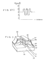
- FIG 4(a) an idealized energy band structure of the strained superlattice laser described by Shieh is schematically shown.
- Quantum barrier layers 13 sandwich quantum well layers 14 of the strained superlattice structure 15.
- the outermost quantum well layers lie adjacent to the respective GaAs light guide layers 17.
- the light guide layers are, in turn, sandwiched by the Al 0.2 Ga 0.8 As cladding layers 12 and 16.
- Figure 4(b) is a graph of the degree of lattice mismatch, ⁇ a/a, as a function of position within the Shieh laser structure where a is the lattice constant of GaAs.
- the graph of Figure 4(b) is plotted as the percent of lattice mismatch.
- AlAs aluminum arsenide
- GaAs GaAs
- the lattice mismatch with the cladding and light guide layers is about plus 1.4 percent for the quantum well layers and zero percent for the quantum barrier layers.
- the strain increases, i.e., accumulates, with each quantum well layer and quantum barrier layer that is grown.
- the total strain within the laser structure constantly increases with additional superlattice layers so that the advantages of the strained superlattice structure gradually decline with an increasing number of quantum wells.
- threshold current density increases with increasing quantum wells and increases unacceptably in a structure including six quantum wells. At that point, the total strain has become so large that it totally overwhelms the improvements achieved by employing the strained superlattice structure.
- a semiconductor structure for a light-interactive semiconductor device includes first and second crystalline semiconductor cladding layers having a first lattice constant and a strained superlattice structure disposed in contact with and between the first and second cladding layers and including alternating first crystalline semiconductor quantum barrier layers having a first energy band gap and a second lattice constant and second crystalline semiconductor quantum well layers having a second energy band gap less than the first energy band gap and a third lattice constant wherein the first lattice constant is approximately equal to the average of the second and third lattice constants and the second lattice constant differs from the third lattice constant by at least about 0.5 percent of the second lattice constant.
- a light-interactive semiconductor device includes a semiconductor substrate, a first crystalline semiconductor cladding layer disposed on the semiconductor substrate and having a first lattice constant, a strained superlattice structure disposed on the first cladding layer and including alternating first crystalline semiconductor quantum barrier layers having a first energy band gap and a second lattice constant and second crystalline semiconductor quantum well layers having a second energy band gap less than the first energy band gap and a third lattice constant wherein the first lattice constant is approximately equal to the average of the second and third lattice constants and the second lattice constant differs from the third lattice constant by at least about 0.5 percent of the second lattice constant, a second crystalline semiconductor cladding layer disposed on the strained superlattice structure opposite the first cladding layer, and first and second electrodes respectively disposed on the first and second cladding layers.
- a semiconductor laser includes a first conductivity type semiconductor substrate, a first conductivity type crystalline semiconductor cladding layer disposed on the semiconductor substrate and having a first lattice constant, a strained superlattice structure disposed on the first cladding layer and including alternating first crystalline semiconductor quantum barrier layers having a first energy band gap and a second lattice constant and second crystalline semiconductor quantum well layers having a second energy band gap less than the first energy band gap and a third lattice constant wherein the first lattice constant is approximately equal to the average of the second and third lattice constants and the second lattice constant differs from the third lattice constant by at least about 0.5 percent of the second lattice con stant, a second conductivity type crystalline semiconductor cladding layer disposed on the strained superlattice structure opposite the first cladding layer, and first and second electrodes respectively disposed on the first and second cladding layers.
- Figure 1 is a schematic cross-sectional view of a semiconductor device including a strained superlattice structure according to the invention.
- Figure 2(a) is an energy band diagram of the strained superlattice structure of Figure 1.
- Figure 2(b) is a graph of the degree of lattice mismatch as a function of position in the strained superlattice structure of Figure 2(a).
- Figure 2(c) is a graph of the degree of lattice mismatch as a function of position in a strained superlattice structure according to the invention.
- Figure 3 is a perspective view, partly in section, of a semiconductor laser incorporating a strained superlattice structure according to an embodiment of the invention.
- Figure 4(a) is an energy band diagram of a portion of a semiconductor laser incorporating a strained superlattice structure active layer according to the prior art.
- Figure 4(b) is a graph of the degree of lattice mismatch as a function of position in the strained superlattice structure of Figure 4(a).
- Figure 1 is a schematic cross-sectional view of a light-interactive semiconductor device incorporating a strained superlattice structure.
- the device includes a substrate 1 on which a cladding layer 2 is disposed.
- a strained superlattice structure 5 is disposed on the cladding layer 2 and includes a plurality of alternatingly disposed quantum barrier layers 3 and quantum well layers 4.
- a second cladding layer 6 is disposed on the strained superlattice structure 5.
- Electrodes 7 and 8 are disposed on the substrate 1 and second cladding layer 6, respectively, for passing a current through the strained superlattice structure transverse to the thicknesses of the layers 3 and 4.
- the substrate 1 may be an n-type indium phosphide (InP) substrate on which the first cladding layer 2 of InP is grown by metal organic chemical vapor deposition (MOCVD).
- MOCVD metal organic chemical vapor deposition
- the strained superlattice structure 5 is formed by alternatingly and successively growing quantum barrier layers 3 of, for example, In 0.35 Ga 0.65 As about 100 Angstroms thick and quantum well layers of, for example, In 0.7 Ga 0.3 As about 100 Angstroms thick.
- eleven quantum barrier layers and ten quantum well layers are grown. These quantum well and quantum barrier layers may be grown by MOCVD or by molecular beam epitaxy (MBE).
- a second cladding layer 6 is grown on the strained superlattice structure 5 and the electrodes 7 and 8 are formed to complete the device structure.
- the substrate 1 and the first cladding layer 2 are of the same conductivity type and the second cladding layer 6 is of a second, opposite conductivity type from the first cladding layer 2.
- FIG. 2(a) An energy band diagram of the central portion of the device of Figure 1 centered about the strained superlattice structure 5 is shown in Figure 2(a).
- the repetitive quantum well and quantum barrier layers 3 and 4 are abbreviated as indicated in Figure 2(a).
- the energy band structure of Figure 2(a) is identical to that of the energy band structure of prior art Figure 4(a), although the number of quantum wells included in the structure of Figure 2(a) is larger.
- Figure 2(b) a graph of the percentage of lattice mismatch within the central portion of the device of Figure 1 is plotted as a function of position within that structure.
- the structural elements of Figure 1 are indicated in the graph of Figure 2(b).
- strain is present within the strained superlattice structure 5 just as it is present in the strained superlattice structure 15 of the prior art structure.
- Figures 2(b) and 4(b) it can be seen that the strain caused by the lattice mismatch does not accumulate in the structure of Figure 1 as it does in the structure of Figure 4(b).
- the lattice mismatches relative to the cladding layer 17 are all in one direction.
- the lattice mismatch at the interface of the cladding layer 6 and the first quantum barrier layer 3 is in one direction, i.e., the lattice constant decreases.
- the lattice mismatch, i.e., strain changes in sign, i.e., direction, to a magnitude approximately equal to the lattice mismatch between the cladding layer 6 and the first quantum barrier layer 4.
- the lattice constant of a ternary crystalline compound semiconductor can be found by interpolating between the lattice constants of the two crystalline binary compound semiconductors from which the ternary compound semiconductor is formed.
- the lattice constant within the prior art strained superlattice structure of Figure 4(a) varies from the GaAs lattice constant of the barrier layers of 5.65 Angstroms to the lattice constant of 5.73 of the ternary compound of the quantum well layers.
- the lattice constant of the quantum barrier layers is 5.78 Angstroms and the lattice constant of the quantum well layers is 5.94 Angstroms.
- the average of those lattice constants substantially equals the lattice constant of 5.87 Angstroms of the InP cladding layers 2 and 6.
- the total strain produced by growing one pair of layers of the superlattice structure is compensated for, to a large degree, by the strain betwreen the second of those layers and the next, i.e., third, layer grown.
- the dislocation density produced in the growth process is controlled so that a relatively large number of quantum well and quantum barrier layers can be grown without cumulative strain that adversely affects the electrical characteristics of a device incorporating the structure.
- the lattice mismatch has an amplitude of about 2 percent and is about plus and minus 1 percent with reference to the lattice constant of the InP cladding layer.
- the desired effects produced by strained superlattice structures have been observed with lattice mismatches of as little as 0.5 percent but have been difficult to observe with lattice mismatches of 0.4 percent and below. Therefore, to produce a strained superlattice structure according to the invention, the degree of lattice mismatch between a cladding layer and the quantum well and quantum barrier layers should be greater than about 0.5 percent, although the minimum degree of mismatch cannot be specified with precision.
- the average of the lattice constants of the quantum well and quantum barrier layers is equal to the lattice constant of the cladding layer, but precise equality is not essential to the invention.
- the lattice constant of the quantum well layers is larger than the lattice constant of the quantum barrier layers.
- that relationship can be reversed so that a graph of the degree of lattice mismatch as a function of position within the structure would be as shown in Figure 2(c).
- the substrate 1 may be an insulating or semi-insulating substrate and other compound semiconductor materials besides InP, such as those listed in the foregoing Table, may be employed as the substrate or in the cladding layers and as part of the ternary semiconductor compounds employed in the quantum well and quantum barrier layers.
- the strained superlattice structure according to the invention may be employed in a large variety of light-interactive semiconductor devices.
- the term "light-interactive" means a semiconductor device that alters a characteristic of a beam of light or that generates light, such as a semiconductor laser.
- the embodiment of the invention shown in Figure 1 functions as an optical waveguide channeling a beam of incident light 9 that is generally transverse to the thicknesses of the quantum well and quantum barrier layers of the strained superlattice structure 5.
- the same device can function as a light beam deflecting device.
- the incident light beam 9 traverses the strained superlattice structure and emerges as light beam 10.
- the device of Figure 1 can function as an optical switch, switching the direction of the incident light beam, and as an optical modulator when only a portion of the incident light beam is deflected from the direction 10 to the direction 11.
- a particularly useful application of the novel strained superlattice structure is in a semiconductor laser, an example of which is shown in a perspective, partially sectioned, view in Figure 3.
- That semiconductor laser includes a p-type InP substrate 20, a p-type InP first cladding layer 21, a strained superlattice structure 5 as the active layer, an n-type InP second cladding layer 22, an n-type InP third cladding layer 26, and an n-type InGaAsP contacting layer 27, all successively disposed.
- a first electrode 29 is disposed on the substrate 20 and a second electrode 30 is disposed on and in electrical contact with the contacting layer 27.
- An insulating film 28 separates the contacting layer 27 from the side surfaces of a mesa that includes a current blocking structure.
- That current blocking structure includes a p-type InP buried region 23 and an n-type InP current blocking layer 24 having a crescent shape and buried within the p-type current blocking region.
- the strained superlattice structure 5 has the same structure as described for the strained superlattice structure 5 of Figure 1, namely, six quantum barrier layers of In 0.35 Ga 0.65 As and five quantum well layers of In 0.7 Ga 0.3 As.
- the laser structure of Figure 3 can be manufactured using known processes. Initially, the first cladding layer 21, the strained superlattice structure 5, and the second cladding layer 22 are successively grown on the substrate 20 by MOCVD. Thereafter, a mesa is formed by masking and etching of the grown layers. After formation of the mesa, the region 23, the current blocking layer 24, the third cladding layer 26, and the contacting layer 27 are sequentially grown by liquid phase epitaxy (LPE). The formation of region 23 actually includes two separate growth steps that result in the crescent shape of the current blocking layer 24. Initially, a p-type InP layer is grown followed by the growth of the n-type current blocking layer 24. Subsequently, another p-type current blocking layer is grown by LPE.
- LPE liquid phase epitaxy
- the semiconductor laser structure of Figure 3 functions in the same manner as the prior art laser described with respect to Figure 4(a), producing laser light in response to a current flow between electrodes 29 and 30 that exceeds the threshold current.
- the number of quantum wells in the strained superlattice structure 5 is not limited by crystallinity considerations and may be any number of quantum wells that produces the desired electrical and optical performance of the laser.
Abstract
Description
- The present invention relates to a strained superlattice semiconductor structure that is light-interactive and particularly to an optical waveguide, a light beam deflecting device, and a semiconductor laser incorporating the strained superlattice semiconductor structure.
- Semiconductor superlattice structures including alternating quantum well and quantum barrier layers are well known. In the basic unit of these structures, a thin semiconductor layer having a relatively narrow energy band gap is sandwiched between thin layers of a different semiconductor material having a relatively wide energy band gap. A quantum well is thus formed in which charge carriers can be confined and from which, under appropriate circumstances, charge carriers can escape by tunneling or another charge carrier transport mechanism. In a multiple quantum well structure, a plurality of these basic units are sequentially disposed. Superlattice structures including one or more quantum wells have found applications in numerous semiconductor devices including semiconductor lasers and other light-interactive devices.
- When the different crystalline semiconductor materials used in the quantum well layers and in the quantum barrier layers have different lattice constants, an atomic mismatch between adjacent crystalline layers occurs. The lattice mismatching of the crystalline structures adjacent each of the quantum well/quantum barrier layer interfaces causes strain in the layers and affects the electrical characteristics of the structure. While considerable effort has been devoted to producing superlattice structures essentially free of strain, in recent years it has been determined that beneficial results can be achieved if some strain is present in a superlattice structure. For example, wavelength of the light produced by a semiconductor laser incorporating a so-called strained superlattice structure as the active layer can be shifted compared to a similar semiconductor laser employing a superlattice structure active layer free of strain. In addition, semiconductor lasers incorporating scrained superlattice structures exhibit lower threshold currents for laser oscillation and lower operating currents than similar semiconductor lasers without superlattice structures.
- While strain in a superlattice structure can produce beneficial effects in a device incorporating the strained superlattice structure, an excessive amount of strain can cause detrimental effects and even prevent device operation. Assuming each quantum well layer and quantum barrier layer interface introduces the same amount of strain into a superlattice structure, the total strain present in prior art structures is equal to the product of that strain and the number of such interfaces in the strained superlattice structure. Generally, the strain at each interface between a quantum well layer and quantum barrier layer is directly related to the difference between the lattice constants of the semiconductor materials employed in the quantum well and quantum barrier layers. When the total strain in a superlattice structure exceeds a critical value, the dislocation density in the semiconductor layers increases significantly, resulting in a severe deterioration of the crystallinity of subsequently grown semiconductor layers that adversely affect the characteristics of a device, such as a laser, incorporating the structure.
- An example of a semiconductor laser incorporating a strained superlattice structure as an active layer was described by Shieh et al in electronics Letters, Volume 18, Number 25, 1989, pages 1226-1228. In that laser structure, cladding layers of Al0.2Ga0.8As sandwiched light guide layers of gallium arsenide (GaAs) which, in turn, sandwiched a strained superlattice structure active layer. The well layers in the strained superlattice structure were Ga0.8In0.2As and the barrier layers were GaAs. Those authors prepared a number of such semiconductor laser structures including 1 and 3-6 quantum wells, respectively.
- In Figure 4(a), an idealized energy band structure of the strained superlattice laser described by Shieh is schematically shown.
Quantum barrier layers 13 sandwichquantum well layers 14 of the strained superlattice structure 15. The outermost quantum well layers lie adjacent to the respective GaAslight guide layers 17. The light guide layers are, in turn, sandwiched by the Al0.2Ga0.8Ascladding layers - Figure 4(b) is a graph of the degree of lattice mismatch, Δa/a, as a function of position within the Shieh laser structure where a is the lattice constant of GaAs. The graph of Figure 4(b) is plotted as the percent of lattice mismatch. Thus, in the
cladding layer 16 and thelight guide layer 17adjacent cladding layer 16, the lattice mismatching is zero because aluminum arsenide (AlAs) and GaAs have essentially the same lattice constant. In the strained superlattice structure 15, the lattice mismatch with the cladding and light guide layers is about plus 1.4 percent for the quantum well layers and zero percent for the quantum barrier layers. In other words, as the strained superlattice structure 15 is grown on thelight guide layer 17, the strain increases, i.e., accumulates, with each quantum well layer and quantum barrier layer that is grown. The total strain within the laser structure constantly increases with additional superlattice layers so that the advantages of the strained superlattice structure gradually decline with an increasing number of quantum wells. In fact, as shown in Shieh's Figure 2, threshold current density increases with increasing quantum wells and increases unacceptably in a structure including six quantum wells. At that point, the total strain has become so large that it totally overwhelms the improvements achieved by employing the strained superlattice structure. - Because of the increasing strain and the adverse effects of strain within a strained superlattice structure as the number of quantum wells is increased, the performance improvement that can be achieved in light-interactive semiconductor devices incorporating strained superlattice structures is limited. These strain limitations prevent the use of an arbitrary number of quantum wells in a strained superlattice structure and limit the practical realization of light-interactive devices incorporating strained superlattice structures.
- It is an object of the invention to provide a strained superlattice semiconductor structure that may include an arbitrary number of quantum wells without the adverse effect of accumulated strain.
- It is another object of the invention to provide a light-interactive semiconductor device including a strained superlattice semiconductor structure that may include an arbitrary number of quantum wells without the adverse effect of accumulated strain.
- It is yet another object of the invention to provide a semiconductor laser including a strained superlattice semiconductor structure that may include an arbitrary number of quantum wells without the adverse effect of accumulated strain.
- A semiconductor structure for a light-interactive semiconductor device according to the invention includes first and second crystalline semiconductor cladding layers having a first lattice constant and a strained superlattice structure disposed in contact with and between the first and second cladding layers and including alternating first crystalline semiconductor quantum barrier layers having a first energy band gap and a second lattice constant and second crystalline semiconductor quantum well layers having a second energy band gap less than the first energy band gap and a third lattice constant wherein the first lattice constant is approximately equal to the average of the second and third lattice constants and the second lattice constant differs from the third lattice constant by at least about 0.5 percent of the second lattice constant.
- A light-interactive semiconductor device according to the invention includes a semiconductor substrate, a first crystalline semiconductor cladding layer disposed on the semiconductor substrate and having a first lattice constant, a strained superlattice structure disposed on the first cladding layer and including alternating first crystalline semiconductor quantum barrier layers having a first energy band gap and a second lattice constant and second crystalline semiconductor quantum well layers having a second energy band gap less than the first energy band gap and a third lattice constant wherein the first lattice constant is approximately equal to the average of the second and third lattice constants and the second lattice constant differs from the third lattice constant by at least about 0.5 percent of the second lattice constant, a second crystalline semiconductor cladding layer disposed on the strained superlattice structure opposite the first cladding layer, and first and second electrodes respectively disposed on the first and second cladding layers.
- A semiconductor laser according to the invention includes a first conductivity type semiconductor substrate, a first conductivity type crystalline semiconductor cladding layer disposed on the semiconductor substrate and having a first lattice constant, a strained superlattice structure disposed on the first cladding layer and including alternating first crystalline semiconductor quantum barrier layers having a first energy band gap and a second lattice constant and second crystalline semiconductor quantum well layers having a second energy band gap less than the first energy band gap and a third lattice constant wherein the first lattice constant is approximately equal to the average of the second and third lattice constants and the second lattice constant differs from the third lattice constant by at least about 0.5 percent of the second lattice con stant, a second conductivity type crystalline semiconductor cladding layer disposed on the strained superlattice structure opposite the first cladding layer, and first and second electrodes respectively disposed on the first and second cladding layers.
- Other objects and advantages of the present invention will become apparent from the detailed description that follows. It should be understood, however, that the detailed description is given by way of illustration only, since various additions and modifications within the spirit and scope of the invention will become apparent to those skilled in the art from the detailed description.
- Figure 1 is a schematic cross-sectional view of a semiconductor device including a strained superlattice structure according to the invention.
- Figure 2(a) is an energy band diagram of the strained superlattice structure of Figure 1.
- Figure 2(b) is a graph of the degree of lattice mismatch as a function of position in the strained superlattice structure of Figure 2(a).
- Figure 2(c) is a graph of the degree of lattice mismatch as a function of position in a strained superlattice structure according to the invention.
- Figure 3 is a perspective view, partly in section, of a semiconductor laser incorporating a strained superlattice structure according to an embodiment of the invention.
- Figure 4(a) is an energy band diagram of a portion of a semiconductor laser incorporating a strained superlattice structure active layer according to the prior art.
- Figure 4(b) is a graph of the degree of lattice mismatch as a function of position in the strained superlattice structure of Figure 4(a).
- Figure 1 is a schematic cross-sectional view of a light-interactive semiconductor device incorporating a strained superlattice structure. The device includes a
substrate 1 on which acladding layer 2 is disposed. Astrained superlattice structure 5 is disposed on thecladding layer 2 and includes a plurality of alternatingly disposedquantum barrier layers 3 andquantum well layers 4. Asecond cladding layer 6 is disposed on thestrained superlattice structure 5.Electrodes 7 and 8 are disposed on thesubstrate 1 andsecond cladding layer 6, respectively, for passing a current through the strained superlattice structure transverse to the thicknesses of thelayers - In one embodiment of the device, the
substrate 1 may be an n-type indium phosphide (InP) substrate on which thefirst cladding layer 2 of InP is grown by metal organic chemical vapor deposition (MOCVD). Thestrained superlattice structure 5 is formed by alternatingly and successively growingquantum barrier layers 3 of, for example, In0.35Ga0.65As about 100 Angstroms thick and quantum well layers of, for example, In0.7Ga0.3As about 100 Angstroms thick. In one exemplary device, eleven quantum barrier layers and ten quantum well layers are grown. These quantum well and quantum barrier layers may be grown by MOCVD or by molecular beam epitaxy (MBE). Finally, asecond cladding layer 6 is grown on thestrained superlattice structure 5 and theelectrodes 7 and 8 are formed to complete the device structure. Generally, thesubstrate 1 and thefirst cladding layer 2 are of the same conductivity type and thesecond cladding layer 6 is of a second, opposite conductivity type from thefirst cladding layer 2. - An energy band diagram of the central portion of the device of Figure 1 centered about the
strained superlattice structure 5 is shown in Figure 2(a). The repetitive quantum well andquantum barrier layers - In Figure 2(b), a graph of the percentage of lattice mismatch within the central portion of the device of Figure 1 is plotted as a function of position within that structure. The structural elements of Figure 1 are indicated in the graph of Figure 2(b). As indicated by the vertical lines in Figure 2(b), strain is present within the
strained superlattice structure 5 just as it is present in the strained superlattice structure 15 of the prior art structure. However, by comparing Figures 2(b) and 4(b), it can be seen that the strain caused by the lattice mismatch does not accumulate in the structure of Figure 1 as it does in the structure of Figure 4(b). - In Figure 4(b), the lattice mismatches relative to the
cladding layer 17 are all in one direction. By contrast, in the structure of Figure 2(b), the lattice mismatch at the interface of thecladding layer 6 and the firstquantum barrier layer 3 is in one direction, i.e., the lattice constant decreases. At the next interface, between the firstquantum barrier layer 3 and the firstquantum well layer 4, the lattice mismatch, i.e., strain, changes in sign, i.e., direction, to a magnitude approximately equal to the lattice mismatch between thecladding layer 6 and the firstquantum barrier layer 4. This alternating pattern in the direction of lattice mismatch relative to thecladding layer 6 with a substantial balance in the magnitudes of the lattice mismatches of opposite directions continues through thestrained superlattice structure 5. In other words, the average of the lattice constants of the quantum well and quantum barrier layers is approximately equal to the lattice constant of the cladding layer. Because of the changes in direction of the lattice mismatches and the substantial balancing of the oppositely directed strains as a result of the mismatches, the accumulated strain with the strained superlattice structure is maintained at a relatively low total value. On the other hand, because of the presence of the lattice mismatches, the desired strain at the interfaces between quantum barrier and quantum well layers is still present in the novel structure. - The desired effect illustrated in Figure 2(b) is achieved by choosing the materials of the cladding, quantum well, and quantum barrier layers considering their respective lattice constants. A brief table of some lattice constants for semiconductor materials illustrates the material selection process.

- According to Vegard's Law, the lattice constant of a ternary crystalline compound semiconductor can be found by interpolating between the lattice constants of the two crystalline binary compound semiconductors from which the ternary compound semiconductor is formed. Applying the foregoing Table, the lattice constant within the prior art strained superlattice structure of Figure 4(a) varies from the GaAs lattice constant of the barrier layers of 5.65 Angstroms to the lattice constant of 5.73 of the ternary compound of the quantum well layers. In the specific embodiment of the invention described above, the lattice constant of the quantum barrier layers is 5.78 Angstroms and the lattice constant of the quantum well layers is 5.94 Angstroms. The average of those lattice constants substantially equals the lattice constant of 5.87 Angstroms of the InP cladding layers 2 and 6. Thus, during the fabrication of the device of Figure 1, the total strain produced by growing one pair of layers of the superlattice structure is compensated for, to a large degree, by the strain betwreen the second of those layers and the next, i.e., third, layer grown. As a result, the dislocation density produced in the growth process is controlled so that a relatively large number of quantum well and quantum barrier layers can be grown without cumulative strain that adversely affects the electrical characteristics of a device incorporating the structure.
- By comparison, if InP were used for the barrier layer of the strained superlattice structure of Figure 1 instead of In0.35Ga0.65As, producing a degree of lattice mismatch graph like that of Figure 4(b), a so-called cross-hatched surface morphology would be produced. That surface morphology indicates a very high density of dislocations that interfere with the crystallinity of the grown layers.
- In the specific example of Figures 1, 2(a), and 2(b), the lattice mismatch has an amplitude of about 2 percent and is about plus and minus 1 percent with reference to the lattice constant of the InP cladding layer. The desired effects produced by strained superlattice structures have been observed with lattice mismatches of as little as 0.5 percent but have been difficult to observe with lattice mismatches of 0.4 percent and below. Therefore, to produce a strained superlattice structure according to the invention, the degree of lattice mismatch between a cladding layer and the quantum well and quantum barrier layers should be greater than about 0.5 percent, although the minimum degree of mismatch cannot be specified with precision. Most preferably, the average of the lattice constants of the quantum well and quantum barrier layers is equal to the lattice constant of the cladding layer, but precise equality is not essential to the invention.
- In the strained superlattice structure described with respect to Figures 1, 2(a), and 2(b), the lattice constant of the quantum well layers is larger than the lattice constant of the quantum barrier layers. However, that relationship can be reversed so that a graph of the degree of lattice mismatch as a function of position within the structure would be as shown in Figure 2(c). Although the embodiment of the invention shown in Figure 1 is described with respect to specific materials and conductivity types, the
substrate 1 may be an insulating or semi-insulating substrate and other compound semiconductor materials besides InP, such as those listed in the foregoing Table, may be employed as the substrate or in the cladding layers and as part of the ternary semiconductor compounds employed in the quantum well and quantum barrier layers. - The strained superlattice structure according to the invention may be employed in a large variety of light-interactive semiconductor devices. As used here, the term "light-interactive" means a semiconductor device that alters a characteristic of a beam of light or that generates light, such as a semiconductor laser. The embodiment of the invention shown in Figure 1, for example, functions as an optical waveguide channeling a beam of incident light 9 that is generally transverse to the thicknesses of the quantum well and quantum barrier layers of the
strained superlattice structure 5. The same device can function as a light beam deflecting device. For example, in the absence of an electrical bias, the incident light beam 9 traverses the strained superlattice structure and emerges as light beam 10. However, when an appropriate electrical bias is applied betweenelectrodes 7 and 8, the characteristics of the optical waveguide formed by thestrained superlattice structure 5 are changed and the light passing through the strained superlattice structure is deflected to thebeam direction 11 indicated in Figure 1. Thus, the device of Figure 1 can function as an optical switch, switching the direction of the incident light beam, and as an optical modulator when only a portion of the incident light beam is deflected from the direction 10 to thedirection 11. - A particularly useful application of the novel strained superlattice structure is in a semiconductor laser, an example of which is shown in a perspective, partially sectioned, view in Figure 3. That semiconductor laser includes a p-
type InP substrate 20, a p-type InPfirst cladding layer 21, astrained superlattice structure 5 as the active layer, an n-type InPsecond cladding layer 22, an n-type InPthird cladding layer 26, and an n-typeInGaAsP contacting layer 27, all successively disposed. Afirst electrode 29 is disposed on thesubstrate 20 and asecond electrode 30 is disposed on and in electrical contact with the contactinglayer 27. An insulatingfilm 28 separates the contactinglayer 27 from the side surfaces of a mesa that includes a current blocking structure. That current blocking structure includes a p-type InP buriedregion 23 and an n-type InPcurrent blocking layer 24 having a crescent shape and buried within the p-type current blocking region. In this semiconductor laser embodiment, thestrained superlattice structure 5 has the same structure as described for thestrained superlattice structure 5 of Figure 1, namely, six quantum barrier layers of In0.35Ga0.65As and five quantum well layers of In0.7Ga0.3As. - The laser structure of Figure 3 can be manufactured using known processes. Initially, the
first cladding layer 21, thestrained superlattice structure 5, and thesecond cladding layer 22 are successively grown on thesubstrate 20 by MOCVD. Thereafter, a mesa is formed by masking and etching of the grown layers. After formation of the mesa, theregion 23, thecurrent blocking layer 24, thethird cladding layer 26, and the contactinglayer 27 are sequentially grown by liquid phase epitaxy (LPE). The formation ofregion 23 actually includes two separate growth steps that result in the crescent shape of thecurrent blocking layer 24. Initially, a p-type InP layer is grown followed by the growth of the n-typecurrent blocking layer 24. Subsequently, another p-type current blocking layer is grown by LPE. In the course of producing that second part of the p-type region 23, some of the n-type layer 24 is dissolved, resulting in the crescent shape of thecurrent blocking layer 24 and, usually, the continuity of the two p-type layers to form the p-type region 23. The semiconductor laser structure of Figure 3 functions in the same manner as the prior art laser described with respect to Figure 4(a), producing laser light in response to a current flow betweenelectrodes strained superlattice structure 5 is not limited by crystallinity considerations and may be any number of quantum wells that produces the desired electrical and optical performance of the laser.
Claims (8)
- A semiconductor structure for a light-interactive semiconductor device comprising:
first and second crystalline semiconductor cladding layers having a first lattice constant; and
a strained superlattice structure disposed in contact with and between the first and second cladding layers and comprising alternating first crystalline semiconductor quantum barrier layers having a first energy band gap and a second lattice constant and second crystalline semiconductor quantum well layers having a second energy band gap less than the first energy band gap and-a third lattice constant wherein the first lattice constant is approximately equal to the average of the second and third lattice constants and the second lattice constant differs from the third lattice constant by at least about 0.5 percent of the second lattice constant. - The semiconductor structure of claim 1 wherein the second lattice constant is larger than the third lattice constant.
- The semiconductor structure of claim 1 wherein the third lattice constant is larger than the second lattice constant.
- The semiconductor structure of claim 1 wherein the first and second cladding layers are InP, the quantum barrier layers are In0.35Ga0.65As, and the quantum well layers are In0.7Ga0.3As.
- The semiconductor structure of claim 1 wherein the strained superlattice structure includes a fixed number of quantum well layers and a number of quantum barrier layers equal to the number of quantum well layers plus one.
- A light-interactive semiconductor device incorporating the semiconductor structure as claimed in any one of claims 1-5, said device comprising also:
a semiconductor substrate supporting said semiconductor structure; and
first and second electrodes arranged one to each side of said semiconductor structure. - A device as claimed in claim 6 wherein:
said first electrode is in contact with the first cladding layer of said semiconductor structure; and
said second electrode is in contact with the surface of said substrate that is opposite to the second cladding layer of said semiconductor substrate. - A semiconductor layer incorporating the light-interactive semiconductor device as claimed in either of claims 6 or 7, wherein:
the first cladding layer of the semiconductor structure incorporated in said device is of one conductivity type; and
the second cladding layer of the semiconductor structure incorporated in said device and the semiconductor substrate of said device are of an opposite conductivity type to said one conductivity type just mentioned.
Applications Claiming Priority (2)
| Application Number | Priority Date | Filing Date | Title |
|---|---|---|---|
| JP2130018A JPH0422185A (en) | 1990-05-17 | 1990-05-17 | Semiconductor optical element |
| JP130018/90 | 1990-05-17 |
Publications (2)
| Publication Number | Publication Date |
|---|---|
| EP0457571A2 true EP0457571A2 (en) | 1991-11-21 |
| EP0457571A3 EP0457571A3 (en) | 1992-01-02 |
Family
ID=15024129
Family Applications (1)
| Application Number | Title | Priority Date | Filing Date |
|---|---|---|---|
| EP19910304364 Withdrawn EP0457571A3 (en) | 1990-05-17 | 1991-05-15 | Strained superlattice semiconductor structure |
Country Status (3)
| Country | Link |
|---|---|
| US (1) | US5181086A (en) |
| EP (1) | EP0457571A3 (en) |
| JP (1) | JPH0422185A (en) |
Cited By (5)
| Publication number | Priority date | Publication date | Assignee | Title |
|---|---|---|---|---|
| EP0557638A2 (en) * | 1992-02-28 | 1993-09-01 | Mitsubishi Denki Kabushiki Kaisha | Semiconductor laser device |
| EP0582942A2 (en) * | 1992-08-04 | 1994-02-16 | Matsushita Electric Industrial Co., Ltd. | A strained multiple quantum well semiconductor laser and a method for producing the same |
| EP0616400A2 (en) * | 1993-03-18 | 1994-09-21 | Fujitsu Limited | Semiconductor laser |
| EP0544357B1 (en) * | 1991-11-26 | 1996-09-04 | Koninklijke Philips Electronics N.V. | Radiation-emitting semiconductor diode |
| WO1996027146A1 (en) * | 1995-02-28 | 1996-09-06 | Siemens Aktiengesellschaft | Integrated optical fibre with an optical layer having a controllable complex refraction index |
Families Citing this family (32)
| Publication number | Priority date | Publication date | Assignee | Title |
|---|---|---|---|---|
| JPH0449688A (en) * | 1990-06-19 | 1992-02-19 | Nec Corp | Strain barrier quantum well semiconductor laser |
| JPH057051A (en) * | 1990-11-09 | 1993-01-14 | Furukawa Electric Co Ltd:The | Quantum barrier semiconductor optical element |
| US5216262A (en) * | 1992-03-02 | 1993-06-01 | Raphael Tsu | Quantum well structures useful for semiconductor devices |
| JP2707183B2 (en) * | 1992-03-12 | 1998-01-28 | 国際電信電話株式会社 | Semiconductor device having strained superlattice |
| US5319660A (en) * | 1992-05-29 | 1994-06-07 | Mcdonnell Douglas Corporation | Multi-quantum barrier laser |
| JPH0629621A (en) * | 1992-07-09 | 1994-02-04 | Mitsubishi Electric Corp | Semiconductor laser device |
| JP2786063B2 (en) * | 1992-08-11 | 1998-08-13 | 日本電気株式会社 | Semiconductor light control device |
| JP2706411B2 (en) * | 1992-12-11 | 1998-01-28 | 古河電気工業株式会社 | Strained quantum well semiconductor laser |
| US5415699A (en) * | 1993-01-12 | 1995-05-16 | Massachusetts Institute Of Technology | Superlattice structures particularly suitable for use as thermoelectric cooling materials |
| US5900071A (en) * | 1993-01-12 | 1999-05-04 | Massachusetts Institute Of Technology | Superlattice structures particularly suitable for use as thermoelectric materials |
| JP2833396B2 (en) * | 1993-01-28 | 1998-12-09 | 松下電器産業株式会社 | Strained multiple quantum well semiconductor laser |
| JP3362356B2 (en) * | 1993-03-23 | 2003-01-07 | 富士通株式会社 | Optical semiconductor device |
| US5769943A (en) * | 1993-08-03 | 1998-06-23 | California Institute Of Technology | Semiconductor apparatus utilizing gradient freeze and liquid-solid techniques |
| US5610366A (en) * | 1993-08-03 | 1997-03-11 | California Institute Of Technology | High performance thermoelectric materials and methods of preparation |
| WO1995015022A1 (en) * | 1993-11-24 | 1995-06-01 | The Furukawa Electric Co., Ltd. | Semiconductor optical element |
| US5559818A (en) * | 1994-03-24 | 1996-09-24 | Sanyo Electric Co., Ltd. | Semiconductor laser device |
| US5491710A (en) * | 1994-05-05 | 1996-02-13 | Cornell Research Foundation, Inc. | Strain-compensated multiple quantum well laser structures |
| US5617436A (en) * | 1995-06-07 | 1997-04-01 | Cornell Research Foundation, Inc. | Strain-compensated multiple quantum well laser structures |
| US5825796A (en) | 1996-09-25 | 1998-10-20 | Picolight Incorporated | Extended wavelength strained layer lasers having strain compensated layers |
| US5719894A (en) * | 1996-09-25 | 1998-02-17 | Picolight Incorporated | Extended wavelength strained layer lasers having nitrogen disposed therein |
| US5719895A (en) * | 1996-09-25 | 1998-02-17 | Picolight Incorporated | Extended wavelength strained layer lasers having short period superlattices |
| US6060656A (en) * | 1997-03-17 | 2000-05-09 | Regents Of The University Of California | Si/SiGe superlattice structures for use in thermoelectric devices |
| US6452206B1 (en) | 1997-03-17 | 2002-09-17 | Massachusetts Institute Of Technology | Superlattice structures for use in thermoelectric devices |
| US6154475A (en) * | 1997-12-04 | 2000-11-28 | The United States Of America As Represented By The Secretary Of The Air Force | Silicon-based strain-symmetrized GE-SI quantum lasers |
| AU764799B2 (en) * | 1997-12-29 | 2003-08-28 | Coretek, Inc. | Microelectromechanically tunable, confocal, vertical cavity surface emitting laser and fabry-perot filter |
| US6330263B1 (en) * | 1998-05-06 | 2001-12-11 | Sarnoff Corporation | Laser diode having separated, highly-strained quantum wells |
| US6060657A (en) * | 1998-06-24 | 2000-05-09 | Massachusetts Institute Of Technology | Lead-chalcogenide superlattice structures |
| US6647041B1 (en) * | 2000-05-26 | 2003-11-11 | Finisar Corporation | Electrically pumped vertical optical cavity with improved electrical performance |
| AU2004300982B2 (en) * | 2003-06-26 | 2007-10-25 | Mears Technologies, Inc. | Semiconductor device including MOSFET having band-engineered superlattice |
| JP5090144B2 (en) | 2006-12-11 | 2012-12-05 | ルネサスエレクトロニクス株式会社 | Embedded semiconductor laser and method of manufacturing the same |
| US9196769B2 (en) | 2013-06-25 | 2015-11-24 | L-3 Communications Cincinnati Electronics Corporation | Superlattice structures and infrared detector devices incorporating the same |
| CN105449017B (en) * | 2015-12-16 | 2017-11-21 | 中国科学院上海微系统与信息技术研究所 | A kind of material structure for being used to realize the extension of InGaAs light absorption wavelengths |
Citations (2)
| Publication number | Priority date | Publication date | Assignee | Title |
|---|---|---|---|---|
| GB2207283A (en) * | 1987-07-02 | 1989-01-25 | Kokusai Denshin Denwa Co Ltd | Semiconductor infrared emitting device |
| EP0353054A2 (en) * | 1988-07-27 | 1990-01-31 | Kokusai Denshin Denwa Kabushiki Kaisha | Quantum well structure and semiconductor device using the same |
Family Cites Families (9)
| Publication number | Priority date | Publication date | Assignee | Title |
|---|---|---|---|---|
| JPS60249380A (en) * | 1984-05-25 | 1985-12-10 | Hitachi Ltd | Semiconductor laser device |
| JPH0650723B2 (en) * | 1984-10-17 | 1994-06-29 | 日本電気株式会社 | Epitaxial growth method |
| JPS61278186A (en) * | 1985-06-03 | 1986-12-09 | Hitachi Ltd | Semiconductor laser device |
| US4804639A (en) * | 1986-04-18 | 1989-02-14 | Bell Communications Research, Inc. | Method of making a DH laser with strained layers by MBE |
| JPS63153887A (en) * | 1986-08-08 | 1988-06-27 | Sharp Corp | Semiconductor laser device |
| JPS63136592A (en) * | 1986-11-26 | 1988-06-08 | Mitsubishi Electric Corp | Semiconductor laser |
| JPS63197391A (en) * | 1987-02-12 | 1988-08-16 | Hitachi Ltd | Semiconductor laser device |
| US5048036A (en) * | 1989-09-18 | 1991-09-10 | Spectra Diode Laboratories, Inc. | Heterostructure laser with lattice mismatch |
| US5012486A (en) * | 1990-04-06 | 1991-04-30 | At&T Bell Laboratories | Vertical cavity semiconductor laser with lattice-mismatched mirror stack |
-
1990
- 1990-05-17 JP JP2130018A patent/JPH0422185A/en active Pending
-
1991
- 1991-05-10 US US07/698,150 patent/US5181086A/en not_active Expired - Lifetime
- 1991-05-15 EP EP19910304364 patent/EP0457571A3/en not_active Withdrawn
Patent Citations (2)
| Publication number | Priority date | Publication date | Assignee | Title |
|---|---|---|---|---|
| GB2207283A (en) * | 1987-07-02 | 1989-01-25 | Kokusai Denshin Denwa Co Ltd | Semiconductor infrared emitting device |
| EP0353054A2 (en) * | 1988-07-27 | 1990-01-31 | Kokusai Denshin Denwa Kabushiki Kaisha | Quantum well structure and semiconductor device using the same |
Non-Patent Citations (4)
| Title |
|---|
| ELECTRONICS LETTERS, vol. 25, no. 18, 31st August 1989, pages 1226-1228, Stevenage, Herts, GB; C. SHIEH et al.: "Critical thickness in strained-layer GaInAs/GaAs quantum well lasers" * |
| ELECTRONICS LETTERS, vol. 26, no. 7, March 1990, pages 465-467, Stevenage, Herts, GB; U. KOREN et al.: "Low threshold highly efficient strained quantum well lasers at 1.5 micrometre wavelength" * |
| IEEE ELECTRON DEVICE LETTERS, vol. EDL-8, no. 5, May 1987, pages 240-242, New York, US; T. KATSUYAMA et al.: "Lifetime test for high-current-injection strained-layer superlattice light-emitting diode" * |
| JOURNAL OF APPLIED PHYSICS, vol. 59, no. 7, April 1986, pages 2447-2450, New York, US; M. QUILLEC et al.: "Growth and characterization of InxGa1-xAs/InyGa1-yAs strained-layer superlattice on InP substrate" * |
Cited By (13)
| Publication number | Priority date | Publication date | Assignee | Title |
|---|---|---|---|---|
| EP0544357B1 (en) * | 1991-11-26 | 1996-09-04 | Koninklijke Philips Electronics N.V. | Radiation-emitting semiconductor diode |
| EP0606127A1 (en) * | 1992-02-28 | 1994-07-13 | Mitsubishi Denki Kabushiki Kaisha | Semiconductor laser device |
| EP0557638A3 (en) * | 1992-02-28 | 1993-11-10 | Mitsubishi Electric Corp | Semiconductor laser device |
| US5272712A (en) * | 1992-02-28 | 1993-12-21 | Mitsubishi Denki Kabushiki Kaisha | Semiconductor laser device |
| EP0557638A2 (en) * | 1992-02-28 | 1993-09-01 | Mitsubishi Denki Kabushiki Kaisha | Semiconductor laser device |
| US5339325A (en) * | 1992-08-04 | 1994-08-16 | Matsushita Electric Industrial Co., Ltd. | Strained multiple quantum well semiconductor laser and a method for producing the same |
| EP0582942A3 (en) * | 1992-08-04 | 1994-04-13 | Matsushita Electric Industrial Co., Ltd. | A strained multiple quantum well semiconductor laser and a method for producing the same |
| EP0582942A2 (en) * | 1992-08-04 | 1994-02-16 | Matsushita Electric Industrial Co., Ltd. | A strained multiple quantum well semiconductor laser and a method for producing the same |
| EP0616400A2 (en) * | 1993-03-18 | 1994-09-21 | Fujitsu Limited | Semiconductor laser |
| EP0616400A3 (en) * | 1993-03-18 | 1995-01-11 | Fujitsu Ltd | Semiconductor laser. |
| US5408487A (en) * | 1993-03-18 | 1995-04-18 | Fujitsu Limited | Semiconductor laser |
| WO1996027146A1 (en) * | 1995-02-28 | 1996-09-06 | Siemens Aktiengesellschaft | Integrated optical fibre with an optical layer having a controllable complex refraction index |
| US5940569A (en) * | 1995-02-28 | 1999-08-17 | Siemens Aktiengesellschaft | Integrated optical element on a substrate of InP |
Also Published As
| Publication number | Publication date |
|---|---|
| EP0457571A3 (en) | 1992-01-02 |
| US5181086A (en) | 1993-01-19 |
| JPH0422185A (en) | 1992-01-27 |
Similar Documents
| Publication | Publication Date | Title |
|---|---|---|
| US5181086A (en) | Strained superlattice semiconductor structure | |
| US5381434A (en) | High-temperature, uncooled diode laser | |
| JP3425185B2 (en) | Semiconductor element | |
| US5577061A (en) | Superlattice cladding layers for mid-infrared lasers | |
| US7016392B2 (en) | GaAs-based long-wavelength laser incorporating tunnel junction structure | |
| EP0206496B1 (en) | Phased array semiconductor laser | |
| US5010374A (en) | Quantum well laser utilizing an inversion layer | |
| US4719155A (en) | Epitaxial layer structure grown on graded substrate and method of growing the same | |
| US4819036A (en) | Semiconductor device | |
| KR0119796B1 (en) | Semiconductor laser | |
| EP0378919B1 (en) | High band-gap opto-electronic device and method for making same | |
| EP0261262B1 (en) | Transverse junction stripe laser | |
| US5594750A (en) | Selectively Si-doped InAs/A1AsSb short-period-superlattices as N-type cladding layers for mid-IR laser structures grown on InAs substrates | |
| JPH0418476B2 (en) | ||
| US4918496A (en) | Infrared emitting device with dislocation free layer | |
| US5204284A (en) | Method of making a high band-gap opto-electronic device | |
| CA2007383C (en) | Semiconductor optical device | |
| US5107514A (en) | Semiconductor optical element | |
| US5422902A (en) | BeTe-ZnSe graded band gap ohmic contact to p-type ZnSe semiconductors | |
| KR920006434B1 (en) | Resonant tunelling barrier structure device | |
| US4631566A (en) | Long wavelength avalanche photodetector | |
| EP0188080B1 (en) | Light-emitting semiconductor device having a super lattice | |
| Kamiyama et al. | Analysis of GaInP/AlGaInP compressive strained multiple-quantum-well laser | |
| EP0457483A2 (en) | Controllable semiconductor modulator having interleaved contacts | |
| US7986721B2 (en) | Semiconductor optical device including a PN junction formed by a second region of a first conductive type semiconductor layer and a second conductive type single semiconductor layer |
Legal Events
| Date | Code | Title | Description |
|---|---|---|---|
| PUAI | Public reference made under article 153(3) epc to a published international application that has entered the european phase |
Free format text: ORIGINAL CODE: 0009012 |
|
| PUAL | Search report despatched |
Free format text: ORIGINAL CODE: 0009013 |
|
| AK | Designated contracting states |
Kind code of ref document: A2 Designated state(s): DE FR GB |
|
| AK | Designated contracting states |
Kind code of ref document: A3 Designated state(s): DE FR GB |
|
| RIN1 | Information on inventor provided before grant (corrected) |
Inventor name: YOSHIDA, NAOHITO, C/O MITSUBISHI DENKI K.K. |
|
| 17P | Request for examination filed |
Effective date: 19920316 |
|
| STAA | Information on the status of an ep patent application or granted ep patent |
Free format text: STATUS: THE APPLICATION HAS BEEN WITHDRAWN |
|
| 18W | Application withdrawn |
Withdrawal date: 19920812 |