EP0455891A1 - Cone electrical contact - Google Patents
Cone electrical contact Download PDFInfo
- Publication number
- EP0455891A1 EP0455891A1 EP90125727A EP90125727A EP0455891A1 EP 0455891 A1 EP0455891 A1 EP 0455891A1 EP 90125727 A EP90125727 A EP 90125727A EP 90125727 A EP90125727 A EP 90125727A EP 0455891 A1 EP0455891 A1 EP 0455891A1
- Authority
- EP
- European Patent Office
- Prior art keywords
- contact
- polymer
- conductive surface
- conical projection
- removeable
- Prior art date
- Legal status (The legal status is an assumption and is not a legal conclusion. Google has not performed a legal analysis and makes no representation as to the accuracy of the status listed.)
- Granted
Links
Images


Classifications
-
- H—ELECTRICITY
- H05—ELECTRIC TECHNIQUES NOT OTHERWISE PROVIDED FOR
- H05K—PRINTED CIRCUITS; CASINGS OR CONSTRUCTIONAL DETAILS OF ELECTRIC APPARATUS; MANUFACTURE OF ASSEMBLAGES OF ELECTRICAL COMPONENTS
- H05K3/00—Apparatus or processes for manufacturing printed circuits
- H05K3/30—Assembling printed circuits with electric components, e.g. with resistor
- H05K3/32—Assembling printed circuits with electric components, e.g. with resistor electrically connecting electric components or wires to printed circuits
- H05K3/325—Assembling printed circuits with electric components, e.g. with resistor electrically connecting electric components or wires to printed circuits by abutting or pinching, i.e. without alloying process; mechanical auxiliary parts therefor
-
- H—ELECTRICITY
- H01—ELECTRIC ELEMENTS
- H01L—SEMICONDUCTOR DEVICES NOT COVERED BY CLASS H10
- H01L23/00—Details of semiconductor or other solid state devices
- H01L23/32—Holders for supporting the complete device in operation, i.e. detachable fixtures
-
- H—ELECTRICITY
- H01—ELECTRIC ELEMENTS
- H01R—ELECTRICALLY-CONDUCTIVE CONNECTIONS; STRUCTURAL ASSOCIATIONS OF A PLURALITY OF MUTUALLY-INSULATED ELECTRICAL CONNECTING ELEMENTS; COUPLING DEVICES; CURRENT COLLECTORS
- H01R4/00—Electrically-conductive connections between two or more conductive members in direct contact, i.e. touching one another; Means for effecting or maintaining such contact; Electrically-conductive connections having two or more spaced connecting locations for conductors and using contact members penetrating insulation
- H01R4/58—Electrically-conductive connections between two or more conductive members in direct contact, i.e. touching one another; Means for effecting or maintaining such contact; Electrically-conductive connections having two or more spaced connecting locations for conductors and using contact members penetrating insulation characterised by the form or material of the contacting members
-
- H—ELECTRICITY
- H01—ELECTRIC ELEMENTS
- H01R—ELECTRICALLY-CONDUCTIVE CONNECTIONS; STRUCTURAL ASSOCIATIONS OF A PLURALITY OF MUTUALLY-INSULATED ELECTRICAL CONNECTING ELEMENTS; COUPLING DEVICES; CURRENT COLLECTORS
- H01R43/00—Apparatus or processes specially adapted for manufacturing, assembling, maintaining, or repairing of line connectors or current collectors or for joining electric conductors
- H01R43/16—Apparatus or processes specially adapted for manufacturing, assembling, maintaining, or repairing of line connectors or current collectors or for joining electric conductors for manufacturing contact members, e.g. by punching and by bending
-
- H—ELECTRICITY
- H05—ELECTRIC TECHNIQUES NOT OTHERWISE PROVIDED FOR
- H05K—PRINTED CIRCUITS; CASINGS OR CONSTRUCTIONAL DETAILS OF ELECTRIC APPARATUS; MANUFACTURE OF ASSEMBLAGES OF ELECTRICAL COMPONENTS
- H05K3/00—Apparatus or processes for manufacturing printed circuits
- H05K3/40—Forming printed elements for providing electric connections to or between printed circuits
- H05K3/4007—Surface contacts, e.g. bumps
-
- H—ELECTRICITY
- H01—ELECTRIC ELEMENTS
- H01L—SEMICONDUCTOR DEVICES NOT COVERED BY CLASS H10
- H01L2924/00—Indexing scheme for arrangements or methods for connecting or disconnecting semiconductor or solid-state bodies as covered by H01L24/00
- H01L2924/0001—Technical content checked by a classifier
- H01L2924/0002—Not covered by any one of groups H01L24/00, H01L24/00 and H01L2224/00
-
- H—ELECTRICITY
- H01—ELECTRIC ELEMENTS
- H01L—SEMICONDUCTOR DEVICES NOT COVERED BY CLASS H10
- H01L2924/00—Indexing scheme for arrangements or methods for connecting or disconnecting semiconductor or solid-state bodies as covered by H01L24/00
- H01L2924/30—Technical effects
- H01L2924/301—Electrical effects
- H01L2924/3011—Impedance
-
- H—ELECTRICITY
- H01—ELECTRIC ELEMENTS
- H01R—ELECTRICALLY-CONDUCTIVE CONNECTIONS; STRUCTURAL ASSOCIATIONS OF A PLURALITY OF MUTUALLY-INSULATED ELECTRICAL CONNECTING ELEMENTS; COUPLING DEVICES; CURRENT COLLECTORS
- H01R13/00—Details of coupling devices of the kinds covered by groups H01R12/70 or H01R24/00 - H01R33/00
- H01R13/02—Contact members
- H01R13/03—Contact members characterised by the material, e.g. plating, or coating materials
-
- H—ELECTRICITY
- H05—ELECTRIC TECHNIQUES NOT OTHERWISE PROVIDED FOR
- H05K—PRINTED CIRCUITS; CASINGS OR CONSTRUCTIONAL DETAILS OF ELECTRIC APPARATUS; MANUFACTURE OF ASSEMBLAGES OF ELECTRICAL COMPONENTS
- H05K2201/00—Indexing scheme relating to printed circuits covered by H05K1/00
- H05K2201/03—Conductive materials
- H05K2201/0302—Properties and characteristics in general
- H05K2201/0317—Thin film conductor layer; Thin film passive component
-
- H—ELECTRICITY
- H05—ELECTRIC TECHNIQUES NOT OTHERWISE PROVIDED FOR
- H05K—PRINTED CIRCUITS; CASINGS OR CONSTRUCTIONAL DETAILS OF ELECTRIC APPARATUS; MANUFACTURE OF ASSEMBLAGES OF ELECTRICAL COMPONENTS
- H05K2201/00—Indexing scheme relating to printed circuits covered by H05K1/00
- H05K2201/03—Conductive materials
- H05K2201/0332—Structure of the conductor
- H05K2201/0335—Layered conductors or foils
- H05K2201/0347—Overplating, e.g. for reinforcing conductors or bumps; Plating over filled vias
-
- H—ELECTRICITY
- H05—ELECTRIC TECHNIQUES NOT OTHERWISE PROVIDED FOR
- H05K—PRINTED CIRCUITS; CASINGS OR CONSTRUCTIONAL DETAILS OF ELECTRIC APPARATUS; MANUFACTURE OF ASSEMBLAGES OF ELECTRICAL COMPONENTS
- H05K2201/00—Indexing scheme relating to printed circuits covered by H05K1/00
- H05K2201/03—Conductive materials
- H05K2201/0332—Structure of the conductor
- H05K2201/0364—Conductor shape
- H05K2201/0367—Metallic bump or raised conductor not used as solder bump
-
- H—ELECTRICITY
- H05—ELECTRIC TECHNIQUES NOT OTHERWISE PROVIDED FOR
- H05K—PRINTED CIRCUITS; CASINGS OR CONSTRUCTIONAL DETAILS OF ELECTRIC APPARATUS; MANUFACTURE OF ASSEMBLAGES OF ELECTRICAL COMPONENTS
- H05K2201/00—Indexing scheme relating to printed circuits covered by H05K1/00
- H05K2201/03—Conductive materials
- H05K2201/0332—Structure of the conductor
- H05K2201/0364—Conductor shape
- H05K2201/0373—Conductors having a fine structure, e.g. providing a plurality of contact points with a structured tool
-
- H—ELECTRICITY
- H05—ELECTRIC TECHNIQUES NOT OTHERWISE PROVIDED FOR
- H05K—PRINTED CIRCUITS; CASINGS OR CONSTRUCTIONAL DETAILS OF ELECTRIC APPARATUS; MANUFACTURE OF ASSEMBLAGES OF ELECTRICAL COMPONENTS
- H05K2201/00—Indexing scheme relating to printed circuits covered by H05K1/00
- H05K2201/20—Details of printed circuits not provided for in H05K2201/01 - H05K2201/10
- H05K2201/209—Auto-mechanical connection between a component and a PCB or between two PCBs
-
- H—ELECTRICITY
- H05—ELECTRIC TECHNIQUES NOT OTHERWISE PROVIDED FOR
- H05K—PRINTED CIRCUITS; CASINGS OR CONSTRUCTIONAL DETAILS OF ELECTRIC APPARATUS; MANUFACTURE OF ASSEMBLAGES OF ELECTRICAL COMPONENTS
- H05K2203/00—Indexing scheme relating to apparatus or processes for manufacturing printed circuits covered by H05K3/00
- H05K2203/03—Metal processing
- H05K2203/0307—Providing micro- or nanometer scale roughness on a metal surface, e.g. by plating of nodules or dendrites
-
- H—ELECTRICITY
- H05—ELECTRIC TECHNIQUES NOT OTHERWISE PROVIDED FOR
- H05K—PRINTED CIRCUITS; CASINGS OR CONSTRUCTIONAL DETAILS OF ELECTRIC APPARATUS; MANUFACTURE OF ASSEMBLAGES OF ELECTRICAL COMPONENTS
- H05K2203/00—Indexing scheme relating to apparatus or processes for manufacturing printed circuits covered by H05K3/00
- H05K2203/07—Treatments involving liquids, e.g. plating, rinsing
- H05K2203/0703—Plating
- H05K2203/072—Electroless plating, e.g. finish plating or initial plating
-
- H—ELECTRICITY
- H05—ELECTRIC TECHNIQUES NOT OTHERWISE PROVIDED FOR
- H05K—PRINTED CIRCUITS; CASINGS OR CONSTRUCTIONAL DETAILS OF ELECTRIC APPARATUS; MANUFACTURE OF ASSEMBLAGES OF ELECTRICAL COMPONENTS
- H05K2203/00—Indexing scheme relating to apparatus or processes for manufacturing printed circuits covered by H05K3/00
- H05K2203/07—Treatments involving liquids, e.g. plating, rinsing
- H05K2203/0703—Plating
- H05K2203/0723—Electroplating, e.g. finish plating
-
- H—ELECTRICITY
- H05—ELECTRIC TECHNIQUES NOT OTHERWISE PROVIDED FOR
- H05K—PRINTED CIRCUITS; CASINGS OR CONSTRUCTIONAL DETAILS OF ELECTRIC APPARATUS; MANUFACTURE OF ASSEMBLAGES OF ELECTRICAL COMPONENTS
- H05K3/00—Apparatus or processes for manufacturing printed circuits
- H05K3/0011—Working of insulating substrates or insulating layers
- H05K3/0017—Etching of the substrate by chemical or physical means
- H05K3/0026—Etching of the substrate by chemical or physical means by laser ablation
- H05K3/0032—Etching of the substrate by chemical or physical means by laser ablation of organic insulating material
- H05K3/0035—Etching of the substrate by chemical or physical means by laser ablation of organic insulating material of blind holes, i.e. having a metal layer at the bottom
-
- H—ELECTRICITY
- H05—ELECTRIC TECHNIQUES NOT OTHERWISE PROVIDED FOR
- H05K—PRINTED CIRCUITS; CASINGS OR CONSTRUCTIONAL DETAILS OF ELECTRIC APPARATUS; MANUFACTURE OF ASSEMBLAGES OF ELECTRICAL COMPONENTS
- H05K3/00—Apparatus or processes for manufacturing printed circuits
- H05K3/36—Assembling printed circuits with other printed circuits
- H05K3/361—Assembling flexible printed circuits with other printed circuits
- H05K3/365—Assembling flexible printed circuits with other printed circuits by abutting, i.e. without alloying process
Definitions
- the present invention relates to an electrical interconnection and means of making the interconnections, which are useful in electronic packaging applications such as in semiconductor integrated circuit chips and circuit boards and cards, cables and modules.
- IBM Technical Disclosure Bulletin Vol. 22, No. 7, p. 2706, published December, 1979 describes a high density pad-to-pad connector on which dendrites are grown on a pad and coated with a liquid gallium alloy. When the dendritic pad is mated, the dendrites pierce the tarnished liquid metal film of a second pad and make the electrical contact.
- US-A-3 634 807 describes a removably attachable contact comprising a plurality of hollow metal spheres or wire balls mounted in a predetermined pattern on either side of a flexible insulating sheet.
- metal is deposited in openings at the intersection of thin strips of insulating material.
- a conductive sheet is sandwiched between sets of contact elements.
- US-A-3 725 845 describes a hermaphroditic connector comprising a plurality of hollow posts. This is a large scale connector for watertight use with cables in geophysical surveying, rather than for use with microminiature contact pads in packaging.
- US-A-3 881 799 describes a connector that comprises a plurality of domes projecting from both sides of a spring matrix, interposing a third element between the contacts to be connected, the third element is integral to neither.
- US-A-4 644 130 describes a plurality of elastomeric connector rods which have been rendered conductive by being filled with conductive particles dispersed therein.
- US-A-4 751 563 describes a method of making a cone shaped structure, having a carbonaceous surface contaminant, using an electron beam.
- a conductive layer is deposited on at least a portion of the cone and over the substrate area around the base of the cone. Then an insulating material is applied overall and any further processing is performed.
- Structures described in this patent are in the nature of through-holes, buried irreversibly within a unitary multilayer structure rather than being removably attached. Since electron beam radiation is used, the material from which the cone is comprised must be photoactive with respect to electron beams.
- the connector of the present invention is reproducible, substantially smooth, of a single preselected height and non-brittle and applicable to interconnection of high density circuitry.
- US-A-4 328 410 describes the removal of polyimide from a metallic substrate with lateral and depth precision and without causing damage to the metallic substrate. It further describes polyimide removal by a CO2 laser in the infrared region. Removal of polyimide by a CO2 laser in the infrared region proceeds by a mechanism different from ablation by excimer laser, such as in the present invention, which occurs in the ultraviolet region.
- Excimer lasers include XeC1, KrF, ArF and XeF lasers.
- US-A-4 508 749 commonly assigned with the present invention, describes the laser ablation of polyimide through a mask, exposing openings having sloped walls. US-A-4 508 749 is incorporated herein by reference for its description of excimer laser ablation of polyimide.
- CFC's chlorofluorocarbons
- Still another object of the invention is to provide a fabrication method to produce an electrical interconnection between two contact surfaces, at least one of which comprises essentially perpendicular conical projections of predetermined pattern and dimensions.
- the electrical interconnection of the present invention comprises a first and a second contact surface, at least one of which includes a conductive substrate having conical conductors extending substantially perpendicularly therefrom.
- the conical conductors comprise a core of polymeric material, as described more fully hereinbelow, having a conductive film thereover.
- the polymeric cones are formed in a laser removable polymer material which is disposed in a thickness predetermined to be equal to the desired height of conical projections to be formed.
- the contact further includes, in electrical contact with the first conductive surface, a substantially electrically continuous conductive material deposited on at least some of the cones, which have been formed in a predetermined pattern by selectively removing polymeric material by laser.
- the conical projections are formed by excimer laser removal of polymer material through a mask of patterned dots.
- the dots are opaque to the laser beam.
- the laser beam is projected through the mask, removing polymer from areas not blocked by the dots.
- the arrangement of dots on the mask predetermines the location of the conical projections in the polymer.
- a second conductive surface is optionally also provided with conical projections designed to wipe and intermesh with those on the first conductive surface and prepared in the same manner.
- the conductive cones extending substantially perpendicularly from their respective conductive substrate, contacted together form the interconnection, which provides contact while being freely attachable and detachable as desired.
- the respective spacing of the conical projections is such that there is mutual "wipe" between contacting conical projections without their breakage, while at the same time surface contaminants are displaced from the conical projections.
- conductive conical projections disposed on only a first conductive surface, are brought into contact with a second conductive surface, forming the electrical interconnection.
- the tips of the conical projections are brought into contact with enough force to displace any contaminants which may be present on the second conductive surface.
- a second conductive surface may, instead of contact pads alone, include conductive through-holes or blind vias, within which contact is made by a connector pin.
- the pin is optionally soldered in place. Then the conical projections, which are disposed on the head of the pin, are brought into contact with a first conductive surface.
- the conical projections are essentially perpendicular in relation to their respective conductive surface.
- the height of the cones is selected in part to be sufficient for any contaminant or dust to reside therebetween when displaced such that the resistance of the interconnection to be formed is not elevated thereby.
- the array of conical projections comprises polymeric conical bodies formed by excimer laser etching or ablation (removal) and having a conductive layer thereon.
- Fig. 1 represents one embodiment of a single sided conical pad-to-pad interconnection.
- the array of conical projections is comprised of polyimide, followed by an adhesion layer of Cr, followed by a conductive layer of one or more of Cu, Ni and Au, for example a first inner conductive layer of Cu, an intermediate conductive layer of Ni and an outer conductive layer of Au.
- the Fig. 2 drawing shows the conical connector in relation to a through-hole in a pad on the circuit board and a contact pad in a flexible circuit card with which it is designed to interconnect.
- the cones of the connector are provided on the head of a connector pin and fit into and make ohmic contact with a first conductive surface at a contact pad.
- the pin end of the connector pin makes ohmic contact with a metallized through hole of a printed circuit board.
- a connector pin is shown with an array of conical projections on the pin head.
- the pin end is brought into contact with a conductive through-hole or blind via and is soldered in place.
- the conical projections are brought into contact with a second conductive surface, completing the interconnection.
- Fig. 4 shows two cone contacts in spaced apart relationship. When the two cone contacts of Fig. 4 are brought together, each conical projection wipes on its nearest neighbor, displacing dirt.
- the dirt may comprise ambient dust or a chemical film.
- Fig. 5 and 6 drawings demonstrate the intimacy of contact achievable with a double sided cone interconnection. As the first and second contact surfaces approach each other, the cones wipe against each other, displacing contaminants.
- the flow chart of Fig. 7 depicts the process of making a conecon of the invention made by the method described in the Examples.
- a film of polyimide which is obtainable in dry sheets in various thicknesses, is bonded to a brass connector pin which, as illustrated, is 2,16 mm (85 mils) long.
- the polyimide film is laser ablated through a projection mask of dots to form an array of polyimide cones on the head part of the connector pin.
- the array thus formed is subjected to plasma etching to remove polyimide debris left behind from the laser ablation, followed by an overall metallization of conductive material selected from a group which will adhere both to the polyimide cones and to the exposed brass of the substrate therebetween.
- Typical polyimide cones are 82,6 ⁇ m (3 mils) high and have a high aspect ratio.
- the chromium adhesion layer is too thin to be seen, but the copper-nickel-gold can be discerned and is uniformly deposited along the topography of the cone.
- the spacing and height of cones are defined by the dirt expected to contaminate the surface of the cones. The smaller the size and quantity of dirt expected, the smaller and denser can be the conical projections in order to maintain a low contact resistance. It is clear that cones from about 50,8 ⁇ m to about 165 ⁇ m (2 to about 6 mils) can be made easily. Heights should be sufficient to permit contamination to reside between cones without interfering with low resistance. Generally, the smaller the contaminant particles expected, the shorter can be the height of the cones.
- Fig. 9a and Fig. 9b show the uniformity of size and the shape of the conical projections.
- the spacing between cones is seen to be controlled, and the tops uniformly shaped after plating.
- the top radius of the cones is 12,7 ⁇ m (1/2 mil).
- the graph of Fig. 10 illustrates that the contact resistance is stable at and above a contact force of about 10 g.
- Each line represents a separate incidence of contact between the conical projections on a first contact surface with the contact pad which comprises a second contact surface and is an indication of the level of reproducibility of the contact resistance.
- Up to 300 contact cycles of up to 20 g of force have been performed with reproducible contact resistance. Cones have been subjected to greater than about 200 g of force without sustaining damage.
- Fig. 11 shows dusted contact 1 exposed to a moderate application of sieved simulated dust, which incorporates particles up to about 82,6 ⁇ m (3 mils).
- Dusted contact 2 was exposed to a reinforcated with a minimum normal contact force of about 14 g was needed to overcome the effect of the dust contamination on the contact resistance, and that the amount of force required to produce similar contact resistance was practically independent of the amount of dust.
- "gray dust" a heterogenous representation of particles and of synthetic fibers such as to be found in carpeted industrial installations. Mean diameter of the fibers was about 63,5 ⁇ m (2.5 mils).
- the worst damage to cones subjected to an amount of force greater than 200 g appears to be a flattening of the rounded tops of some of the cones, even though the flat contact pad can be seen to be extensively punctured by the cones. It is evident from these SEMs that the cones are strong without being brittle, despite a high aspect ratio.
- Vacrel is a trademark of E. I. du Pont de Nemours and Company for a dry photopolymer film.
- An interconnect having pin-type conical interconnection (“conecon”) has been prepared by the following method:
- a brass connector pin (“conecon blank”) was placed in a holder made of Teflon, polytetrafluorethylene, (a registered trademark of E.I. Dupont de Nemours & Co.), selected for its inertness and designed to hold the pin by the stem.
- a cleaning solution consisting of approximately two tablespoons of Sparkleen in 500 ml. deionized (DI) water was prepared (Sparkleen is a trademark of Fisher Scientific). Sparkleen is a sodium phosphate based laboratory glassware detergent. The polytetrafluorethylene holder and conecon blanks were immersed in the Sparkleen detergent solution for 30 minutes with vigorous stirring, then removed and rinsed in flowing DI water for one minute and rinsed twice more in a beaker of DI water. The rinse was intended to be as thorough as possible, and other rinsing protocols are expected to be equally effective.
- DI deionized
- the conecon blanks were transferred to a Buchner funnel having a fritted disk, washed twice with 100 ml DI water, washed twice with 50 ml methanol and once with acetone.
- the purpose of the methanol was to remove the DI water.
- a wide variety of other solvents having high vapor pressure and water solubility could be used equally successfully to remove the water.
- the conecon blanks were dried under flowing nitrogen gas, then loaded into a second polytetrafluorethylene holder designed so that the heads of the conecon blanks would be nearly flush with the top surface of the holder.
- the conecon blanks and the second polytetrafluorethylene holder were placed in a deaerated, approximately 6 molar HCl solution.
- the HCl solution was maintained under a blanket of nitrogen gas while the conecon blanks were etching in the HCl solution under vigorous stirring.
- the 6 molar HCl concentration is not critical, but was chosen because the etch was completed at room temperature in a reasonable time at that concentration.
- the etched conecon blanks and second polytetrafluorethylene holder were removed from the HCl solution and placed in an approximately 2 molar nitric acid solution for 5 minutes, with stirring.
- the time and concentration of HNO3 are not critical having been chosen to dissolve copper oxide in a reasonable time.
- the etched conecon blanks and second polytetrafluorethylene holder were washed under flowing DI water for one minute, then submersed in flowing DI water for one minute.
- the etched and rinsed conecon blanks were mechanically wiped, transferred to a Buchner funnel with fritted disk and washed as follows to remove residual metal salts, organics and acids, and to assist in drying: (a) three times with 50 ml deionized DI H2O; (b) twice with 50 ml methanol; and (c) twice with 50 ml acetone.
- the conditions of this rinse cycle are intended to be sufficient to remove all water.
- the etched conecons were then dried in flowing N2.
- the dried conecon blanks were manually loaded into the processing fixture to hold them for further processing.
- PI film was laminated onto the head of the conecon in a thickness sufficient to obtain the cone height desired, which for this test was 82,6 ⁇ (3 mils).
- the adhesive used was Flex-i-mid, a trademark of Rogers Corporation, Rogers, CT.
- the PI was hot pressed to the head of the conecon blank in a tool press at 555K (540 degrees F), for 2 minutes at 34,475 mbar (50 psi) followed by 10 minutes more at 344,75 mbar (500 psi), and allowed to cool for 40 minutes at a rate of 5 degrees/minute.
- the press was removed and the PI was postbaked for 30 minutes at 478K (400 degrees F), plus 30 minutes at 533K (500 degrees F), plus 30 minutes at 549K (600 degrees F).
- the polymer in addition to being applied as dry film, may be provided in solution form and may be applied by spinning, spraying or dipping followed by at least partial cure or solidification as is conventional depending on the particular polyimide and the desired height of the cones.
- the excimer laser optics were cleaned and aligned. Any projection system which creates an image through a mask and increases fluence on a target could be used. However, in the present case a -.25X telecentric doublet was used as a projection lens.
- the mask used was Chromium on quartz, comprising an array of Cr dots on a clear background, surrounded by blanket Cr. However, any mask opaque to the laser and not damaged thereby would work as well.
- the focal plane of the system was found by using a fluorescing photoresist.
- the conecon fixture with Flex-i-mid adhered polyimide laminate conecons was placed on its mount and the optical elements moved so that image plane and PI surface coincided.
- a selected conecon was aligned to the mask and the PI was ablated to produce cones.
- the fixture was stepped to the next conecon and the process repeated in series until all the conecons were laser etched. Polymer was simultaneously removed by the laser from the portions of the contact between the cones.
- the cones thus produced were smooth, with sloped walls, and all were of a height of about 101,6 ⁇ m (4 mils), base diameter of about 25,4 ⁇ m (1 mil) as ablated.
- the tops were pointed and domed.
- the debris left behind from the laser ablation of the polyimide was plasma cleaned in an LFE 1002 barrel reactor chamber.
- the system was warmed up and parts were loaded.
- the chamber was pumped down and the gas mixture was bled into the chamber.
- the gas mixture comprised by volume about 27% CF4, 68% 02 and 5% N2.
- the power, rate of gas flow and pressure level were optimized for the system and the parts were treated until clean.
- the conecon parts were sputter cleaned in a plasma chamber in order to promote better adhesion.
- the conecon parts were preheated with infrared lamps to raise their temperature and promote outgassing before the metallization, thereby further improving adhesion.
- 15 nm of chromium for adhesion followed by 4 ⁇ m of copper were applied to the ablated cones using a Leybold Z600 sputtering system.
- the parts were allowed to cool under nitrogen for about 10 minutes and then removed.
- the conecons were deoxidized in a dilute solution of sulfuric acid, rinsed in DI water and plated in an electroless nickel solution. Approximately 5,08 ⁇ m (0.2 mils) of electroless nickel was applied to the conecon The nickel plated conecons were rinsed in DI water, then rinsed in dilute H2SO4 and DI water rinsed again. The nickel plating was followed by an overplate of 2,54 ⁇ m (0.1 mils) pulse electroplated cobalt hardened gold. The object was DC pulse plated in the hardened gold solution according to the following cycle:
- the gold plated conecons were then rinsed to remove cyanate ions using tapwater, and were forced air dried.
- a low temperature solder can be plated, such as prior to electroless nickel, and can be reflowed in order to improve the lateral strength of the cones by about a factor of two. Lateral strength is important in order for the cones to withstand differential thermal expansion.
- the cone connectors of the invention were exposed to Instron testing in a Model 1125 and 4-point probe resistance measurement in order to ascertain the ability of the cone connectors to withstand the repeated contact cycling and to determine the effect of dust, contact pressure and the number of cones making contact.
- the SEMs were obtained using a Cambridge Instruments S250 Mark II scanning electron microscope.
Abstract
Description
- The present invention relates to an electrical interconnection and means of making the interconnections, which are useful in electronic packaging applications such as in semiconductor integrated circuit chips and circuit boards and cards, cables and modules.
- Recent developments in integrated circuits have clearly demonstrated the benefits which can be achieved by fabricating electrical devices into smaller and smaller packages. These small packages are densely packed, being multilevel with signal and power planes and other features on various levels and means of interconnecting selected levels to one another. The interconnections themselves provide sites for potential signal degradation. For example, interconnections between levels of conductor lines, and between conductor lines of a printed circuit board (PCB) or card and any electrical devices mounted thereon can be made between conductive areas called pads. Impedance matching, minimum number of discontinuities and redundancy must be present at these interconnections in order to permit rapid, low noise, low loss, low resistance signal transmission. Approaches used at present in devising interconnections for these electronic packages require several photolithographic masking and etching steps, and the attachment of surface mounted devices may require soldering and rework, often involving exposing the components to destructive temperature cycling.
- Electrical interconnections comprised of interdigitated dendritic projections are a fertile field of scientific inquiry. The conical projections of the present invention are distinguished from dendritic projections by the method of making, by composition, by the controlled location and dimensions of conical projections. Schemes proposed to strengthen dendrites, such as coating with soft metal are described in IBM TDB Vol. 22, No. 7, p. 2706 and copending application serial number 07/415,435, filed September 28, 1989 and commonly assigned with the present invention.
- IBM Technical Disclosure Bulletin Vol. 22, No. 7, p. 2706, published December, 1979 describes a high density pad-to-pad connector on which dendrites are grown on a pad and coated with a liquid gallium alloy. When the dendritic pad is mated, the dendrites pierce the tarnished liquid metal film of a second pad and make the electrical contact.
- IBM Technical Disclosure Bulletin, Vol. 24, No. 1A, June, 1981, p. 2, "Process For Producing Palladium Structures" describes that the small cross-section of the base of the dendrite is at least partly to blame for breakage of dendrites. It also describes the need for "wipe" to make low resistance contact, but states that the roughness of the dendritic surfaces provides sufficient wipe.
- IBM Technical Disclosure Bulletin, Vol. 23, No. 8, January, 1981, p. 1, "Dendrite Connector System With Reinforced Base" agrees with the above diagnosis, but differs in the proposed cure, proposing instead reflowing tin around the bases of the dendrites. Dendrites as pad-to-pad contact elements are also described in Research Disclosure, March, 1988, No. 287, p. 28748, "Method to Provide Multiple Dendritic Contact Points for High Density Flat on Flat Connector System". Again, the dendrites, described are irregularly shaped and randomly located. However, the reduced connector length of the dendrites are described as providing noise reduction and improved signal speed, and the references suggests that having multiple contact points lowers contact resistance.
- Other means in the art of making electrical interconnection between contact pads include spheres US-A-3 634 807 and US-A-4 604 644, conductive rods US-A-4 644 130, US-A-4 050 756 and US-A-4 240 198, hollow posts US-A-3 725 845 and third structures interposed between and parallel to the connector pads but separate from both US-A-3 881 799 and US-A-3 634 807.
- Flat-topped protrusions, permanently connecting pads between levels in a multilayer structure are described in the art, US-A-4 751 563.
- US-A-3 634 807 describes a removably attachable contact comprising a plurality of hollow metal spheres or wire balls mounted in a predetermined pattern on either side of a flexible insulating sheet. Alternatively, metal is deposited in openings at the intersection of thin strips of insulating material. In another embodiment, a conductive sheet is sandwiched between sets of contact elements. These embodiments are designed to be relatively inflexible in the X-Y direction and flexible in the Z direction. These structures are inadequate for high packing density structures, being of dimensions which are too large and too vulnerable to dirt contamination.
- US-A-3 725 845 describes a hermaphroditic connector comprising a plurality of hollow posts. This is a large scale connector for watertight use with cables in geophysical surveying, rather than for use with microminiature contact pads in packaging.
- US-A-3 881 799 describes a connector that comprises a plurality of domes projecting from both sides of a spring matrix, interposing a third element between the contacts to be connected, the third element is integral to neither.
- US-A-4 644 130 describes a plurality of elastomeric connector rods which have been rendered conductive by being filled with conductive particles dispersed therein.
- US-A-4 751 563 describes a method of making a cone shaped structure, having a carbonaceous surface contaminant, using an electron beam. A conductive layer is deposited on at least a portion of the cone and over the substrate area around the base of the cone. Then an insulating material is applied overall and any further processing is performed. Structures described in this patent are in the nature of through-holes, buried irreversibly within a unitary multilayer structure rather than being removably attached. Since electron beam radiation is used, the material from which the cone is comprised must be photoactive with respect to electron beams.
- Unlike connectors described in the art, the connector of the present invention is reproducible, substantially smooth, of a single preselected height and non-brittle and applicable to interconnection of high density circuitry.
- Independent of the electrical connection art, it is known that polyimide, along with certain other polymers, is removable by laser radiation, US-A-4 328 410, US-A-4 508 749 and Research Disclosure, January, 1988, No. 285, p. 28,569, and that irregular conical formations can inadvertently be obtained by laser ablation of a polyimide, ("Development and Origin of Conical Structures on XeC1 Laser Ablated Polyimide", App. Phys. Letter 49(8), August 25, 1986, pp. 453-455). In the latter reference, cones were only formed in laser ablation of polyimide when impurities were present in the polyimide either unintentionally or were deliberately added as a "seed" of particulate impurities.
- US-A-4 328 410 describes the removal of polyimide from a metallic substrate with lateral and depth precision and without causing damage to the metallic substrate. It further describes polyimide removal by a CO₂ laser in the infrared region. Removal of polyimide by a CO₂ laser in the infrared region proceeds by a mechanism different from ablation by excimer laser, such as in the present invention, which occurs in the ultraviolet region. Excimer lasers include XeC1, KrF, ArF and XeF lasers.
- An improvement to the laser ablation rate of polyimide and other polymers by adding dye is described in Research Disclosure, January 1988, No. 285, p. 28,569, "Doped Polyimide Etching By Laser Ablation". IBM TDB Vol. 30, No. 11, April 1988, p. 191, "Removal of Debris Left By Ablative Photodecomposition Of Polymers" describes several ways to remove any debris that may be generated when polyimide or other polymer is removed by laser.
- US-A-4 508 749 commonly assigned with the present invention, describes the laser ablation of polyimide through a mask, exposing openings having sloped walls. US-A-4 508 749 is incorporated herein by reference for its description of excimer laser ablation of polyimide.
- "Novel Method for Measuring Excimer Laser Ablation Thresholds of Polymers" in App. Phys. Lett. 52 (22) May 30, 1988, pp. 1880-1882 describes control of morphological features, including cones, on laser ablated polyimide and other polymers which have, unlike the present invention, been "seeded". In neither of the references is an electrical interconnection suggested or implied. "Structural Origin of Surface Morphological Modification Developed on Poly(ethylene terephthalate) (PET) by Excimer Laser Photoablation" in J. Appl. Phys. 64(1), July 1, 1988, pp. 365-370 also describes seeding and ablation by XeC1 lasers. However, the formation of cones in PI and PET during laser ablation is attributed to redeposition of debris, mostly carbon, in "The Effect of Debris Formation on the Morphology of Excimer Laser Ablated Polymers" in J. App. Phys. 64(5) September 1, 1988, pp. 2815-2818.
- In each of these journal publications, the formation of cones is regarded as undesirable, a phenomenon to be avoided.
- Some processes used in fabricating electronic interconnections use chlorofluorocarbons (CFC's). Thus, it is one object of the invention to use laser mask technology rather than photolithography.
- It is a further object of the invention to provide the capability to interconnect high density packages of electrically mounted devices and PCBs and/or cards to each other and to cables.
- It is a further object of the invention to provide an electrical interconnection which permits reliable, rapid, dirt tolerant, low noise, low loss, low resistance signal transmission.
- It is still a further object of the invention to provide a method of making the electrical interconnection described above in an efficient and controllable manner.
- It is therefore an object of this invention to provide a conical electrical interconnection useful in the art of electronic packaging.
- It is a further object of the invention to provide a conical, low resistance electrical interconnection which has a measure of flexibility and is nondestructively connectable and disconnectable.
- Still another object of the invention is to provide a fabrication method to produce an electrical interconnection between two contact surfaces, at least one of which comprises essentially perpendicular conical projections of predetermined pattern and dimensions.
- These and other objects, features and advantages of the present invention will become more apparent from the descriptions to follow.
- The electrical interconnection of the present invention comprises a first and a second contact surface, at least one of which includes a conductive substrate having conical conductors extending substantially perpendicularly therefrom. The conical conductors comprise a core of polymeric material, as described more fully hereinbelow, having a conductive film thereover.
- The polymeric cones are formed in a laser removable polymer material which is disposed in a thickness predetermined to be equal to the desired height of conical projections to be formed. The contact further includes, in electrical contact with the first conductive surface, a substantially electrically continuous conductive material deposited on at least some of the cones, which have been formed in a predetermined pattern by selectively removing polymeric material by laser.
- The conical projections are formed by excimer laser removal of polymer material through a mask of patterned dots. The dots are opaque to the laser beam.
- The laser beam is projected through the mask, removing polymer from areas not blocked by the dots. The arrangement of dots on the mask predetermines the location of the conical projections in the polymer. A second conductive surface is optionally also provided with conical projections designed to wipe and intermesh with those on the first conductive surface and prepared in the same manner. The conductive cones extending substantially perpendicularly from their respective conductive substrate, contacted together form the interconnection, which provides contact while being freely attachable and detachable as desired.
- In a double-sided embodiment, wherein conical projections disposed on a first conductive substrate are brought into interdigitated contact with like conical projections similarly disposed on a second conductive substrate, the respective spacing of the conical projections is such that there is mutual "wipe" between contacting conical projections without their breakage, while at the same time surface contaminants are displaced from the conical projections.
- Contact is further facilitated by the shaping of the top of each of the conical projections, which are sharply domed, and by the fact that in operation a typical conical projection is in contact with four nearest neighbor cones.
- In a single-sided embodiment, conductive conical projections, disposed on only a first conductive surface, are brought into contact with a second conductive surface, forming the electrical interconnection. The tips of the conical projections are brought into contact with enough force to displace any contaminants which may be present on the second conductive surface.
- Alternatively, in a pin-type conical interconnection, a second conductive surface may, instead of contact pads alone, include conductive through-holes or blind vias, within which contact is made by a connector pin. The pin is optionally soldered in place. Then the conical projections, which are disposed on the head of the pin, are brought into contact with a first conductive surface.
- The conical projections are essentially perpendicular in relation to their respective conductive surface. The height of the cones is selected in part to be sufficient for any contaminant or dust to reside therebetween when displaced such that the resistance of the interconnection to be formed is not elevated thereby.
- Ways of carrying out the invention are described in detail below with reference to drawings which illustrate only specific embodiments in which:
- Fig. 1
- shows one embodiment of a single sided cone connector which, in combination with a substantially planar connector, comprises a single sided conical pad-to-pad interconnection.
- Fig. 2
- shows another embodiment of the single sided cone connector, a pin-type referred to as a conecon.
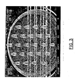
- Fig. 3
- shows a scanning electron micrograph (SEM) at 85 degree tilt of an array of the conical projections of the pin-type embodiment of the present invention after laser ablation but prior to metallization. The scale is on the photograph.
- Fig. 4
- shows an embodiment of a pad-on-pad double sided cone connector.
- Fig. 5
- shows a cross section parallel to the cone axis of the cone connector of Fig. 4 during interconnection.
- Fig. 6
- shows a cross section of the Fig. 5 interconnection, perpendicular to the cone axis.
- Fig. 7
- shows schematically the step in the process of making the connector shown in Fig. 3.
- Fig. 8
- shows a magnified cross sectional view of an actual cone in an array prepared as described above for Fig. 7.
- Fig. 9a
- shows, after metallization, an SEM of one region of a cone array prepared by the method of the invention. Tilt is 35 degrees; the scale is on the photograph.
- Fig. 9b
- shows, after metallization, an SEM of one region of a cone array prepared by the method of the invention. Tilt is 85 degrees; the scale is on the photograph.
- Fig. 10
- shows the contact resistance in mΩ of the single sided cone connector as a function of contact force.
- Fig. 11
- shows a comparison of the contact resistance in mΩ of a single sided cone connector as a function of contact force when there is dirt present compared to a clean contact.
- Fig. 12, a and b,
- shows an SEM of the result of applying excess contact force between the cone array surface of a single sided cone connector and the flat contact pad surface.
- Fig. 13
- shows an SEM of an array before metallization of laser ablated cones. The cones are 165µm (6.5 mils) high, tilt is 64 degrees.
- The array of conical projections comprises polymeric conical bodies formed by excimer laser etching or ablation (removal) and having a conductive layer thereon.
- Fig. 1 represents one embodiment of a single sided conical pad-to-pad interconnection. The array of conical projections is comprised of polyimide, followed by an adhesion layer of Cr, followed by a conductive layer of one or more of Cu, Ni and Au, for example a first inner conductive layer of Cu, an intermediate conductive layer of Ni and an outer conductive layer of Au.
- The Fig. 2 drawing shows the conical connector in relation to a through-hole in a pad on the circuit board and a contact pad in a flexible circuit card with which it is designed to interconnect.
- The cones of the connector are provided on the head of a connector pin and fit into and make ohmic contact with a first conductive surface at a contact pad. The pin end of the connector pin makes ohmic contact with a metallized through hole of a printed circuit board.
- Referring to Fig. 3, a connector pin is shown with an array of conical projections on the pin head. In typical operation as an electrical interconnection, the pin end is brought into contact with a conductive through-hole or blind via and is soldered in place. The conical projections are brought into contact with a second conductive surface, completing the interconnection.
- Fig. 4 shows two cone contacts in spaced apart relationship. When the two cone contacts of Fig. 4 are brought together, each conical projection wipes on its nearest neighbor, displacing dirt. The dirt may comprise ambient dust or a chemical film.
- The Fig. 5 and 6 drawings demonstrate the intimacy of contact achievable with a double sided cone interconnection. As the first and second contact surfaces approach each other, the cones wipe against each other, displacing contaminants.
- The flow chart of Fig. 7 depicts the process of making a conecon of the invention made by the method described in the Examples. As shown in the Fig., a film of polyimide, which is obtainable in dry sheets in various thicknesses, is bonded to a brass connector pin which, as illustrated, is 2,16 mm (85 mils) long. The polyimide film is laser ablated through a projection mask of dots to form an array of polyimide cones on the head part of the connector pin. The array thus formed is subjected to plasma etching to remove polyimide debris left behind from the laser ablation, followed by an overall metallization of conductive material selected from a group which will adhere both to the polyimide cones and to the exposed brass of the substrate therebetween.
- The resulting polyimide conical projections are shown in the Fig. 8 cross-sectional photograph. Typical polyimide cones are 82,6 µm (3 mils) high and have a high aspect ratio. The chromium adhesion layer is too thin to be seen, but the copper-nickel-gold can be discerned and is uniformly deposited along the topography of the cone. The spacing and height of cones are defined by the dirt expected to contaminate the surface of the cones. The smaller the size and quantity of dirt expected, the smaller and denser can be the conical projections in order to maintain a low contact resistance. It is clear that cones from about 50,8 µm to about 165 µm (2 to about 6 mils) can be made easily. Heights should be sufficient to permit contamination to reside between cones without interfering with low resistance. Generally, the smaller the contaminant particles expected, the shorter can be the height of the cones.
- Fig. 9a and Fig. 9b show the uniformity of size and the shape of the conical projections. The spacing between cones is seen to be controlled, and the tops uniformly shaped after plating. The top radius of the cones is 12,7 µm (1/2 mil).
- The graph of Fig. 10 illustrates that the contact resistance is stable at and above a contact force of about 10 g. Each line represents a separate incidence of contact between the conical projections on a first contact surface with the contact pad which comprises a second contact surface and is an indication of the level of reproducibility of the contact resistance. Up to 300 contact cycles of up to 20 g of force have been performed with reproducible contact resistance. Cones have been subjected to greater than about 200 g of force without sustaining damage.
- Fig. 11 shows dusted
contact 1 exposed to a moderate application of sieved simulated dust, which incorporates particles up to about 82,6 µm (3 mils). Dustedcontact 2 was exposed to a redusting of the same dust in an extremely heavy amount. No attempt was made to quantify the amount of dust. The graph shows that a minimum normal contact force of about 14 g was needed to overcome the effect of the dust contamination on the contact resistance, and that the amount of force required to produce similar contact resistance was practically independent of the amount of dust. Experiments were also performed using "gray dust", a heterogenous representation of particles and of synthetic fibers such as to be found in carpeted industrial installations. Mean diameter of the fibers was about 63,5 µm (2.5 mils). - As seen in Figs. 12a and 12b, the worst damage to cones subjected to an amount of force greater than 200 g appears to be a flattening of the rounded tops of some of the cones, even though the flat contact pad can be seen to be extensively punctured by the cones. It is evident from these SEMs that the cones are strong without being brittle, despite a high aspect ratio.
- The conical projections of Fig. 13 have been laser ablated, but not yet metallized, in a layer of Vacrel which is 165 µm (6.5 mils) thick. Vacrel is a trademark of E. I. du Pont de Nemours and Company for a dry photopolymer film.
- It should also be noted in general that the narrower the tips of the cones, the better the contact that can be made. However, the broader the base, the more resistant are the cones expected to be to Z (lateral) forces.
- An interconnect having pin-type conical interconnection ("conecon") has been prepared by the following method:
- A brass connector pin ("conecon blank") was placed in a holder made of Teflon, polytetrafluorethylene, (a registered trademark of E.I. Dupont de Nemours & Co.), selected for its inertness and designed to hold the pin by the stem.
- A cleaning solution consisting of approximately two tablespoons of Sparkleen in 500 ml. deionized (DI) water was prepared (Sparkleen is a trademark of Fisher Scientific). Sparkleen is a sodium phosphate based laboratory glassware detergent. The polytetrafluorethylene holder and conecon blanks were immersed in the Sparkleen detergent solution for 30 minutes with vigorous stirring, then removed and rinsed in flowing DI water for one minute and rinsed twice more in a beaker of DI water. The rinse was intended to be as thorough as possible, and other rinsing protocols are expected to be equally effective.
- The conecon blanks were transferred to a Buchner funnel having a fritted disk, washed twice with 100 ml DI water, washed twice with 50 ml methanol and once with acetone. The purpose of the methanol was to remove the DI water. A wide variety of other solvents having high vapor pressure and water solubility could be used equally successfully to remove the water.
- The conecon blanks were dried under flowing nitrogen gas, then loaded into a second polytetrafluorethylene holder designed so that the heads of the conecon blanks would be nearly flush with the top surface of the holder.
- The conecon blanks and the second polytetrafluorethylene holder were placed in a deaerated, approximately 6 molar HCl solution. The HCl solution was maintained under a blanket of nitrogen gas while the conecon blanks were etching in the HCl solution under vigorous stirring. The 6 molar HCl concentration is not critical, but was chosen because the etch was completed at room temperature in a reasonable time at that concentration.
- After 24 hours the etched conecon blanks and second polytetrafluorethylene holder were removed from the HCl solution and placed in an approximately 2 molar nitric acid solution for 5 minutes, with stirring. The time and concentration of HNO₃ are not critical having been chosen to dissolve copper oxide in a reasonable time. The etched conecon blanks and second polytetrafluorethylene holder were washed under flowing DI water for one minute, then submersed in flowing DI water for one minute.
- The etched and rinsed conecon blanks were mechanically wiped, transferred to a Buchner funnel with fritted disk and washed as follows to remove residual metal salts, organics and acids, and to assist in drying: (a) three times with 50 ml deionized DI H2O; (b) twice with 50 ml methanol; and (c) twice with 50 ml acetone. The conditions of this rinse cycle are intended to be sufficient to remove all water.
- The etched conecons were then dried in flowing N2.
- The dried conecon blanks were manually loaded into the processing fixture to hold them for further processing.
- PI film was laminated onto the head of the conecon in a thickness sufficient to obtain the cone height desired, which for this test was 82,6 µ (3 mils). The type of PI used, Kapton, was treated with an adhesive to bond between PI and the brass connector pin. The adhesive used was Flex-i-mid, a trademark of Rogers Corporation, Rogers, CT. The PI was hot pressed to the head of the conecon blank in a tool press at 555K (540 degrees F), for 2 minutes at 34,475 mbar (50 psi) followed by 10 minutes more at 344,75 mbar (500 psi), and allowed to cool for 40 minutes at a rate of 5 degrees/minute. The press was removed and the PI was postbaked for 30 minutes at 478K (400 degrees F), plus 30 minutes at 533K (500 degrees F), plus 30 minutes at 549K (600 degrees F). It will be obvious to one skilled in the art that the polymer, in addition to being applied as dry film, may be provided in solution form and may be applied by spinning, spraying or dipping followed by at least partial cure or solidification as is conventional depending on the particular polyimide and the desired height of the cones.
- The excimer laser optics were cleaned and aligned. Any projection system which creates an image through a mask and increases fluence on a target could be used. However, in the present case a -.25X telecentric doublet was used as a projection lens. The mask used was Chromium on quartz, comprising an array of Cr dots on a clear background, surrounded by blanket Cr. However, any mask opaque to the laser and not damaged thereby would work as well. The focal plane of the system was found by using a fluorescing photoresist. The conecon fixture with Flex-i-mid adhered polyimide laminate conecons was placed on its mount and the optical elements moved so that image plane and PI surface coincided. A selected conecon was aligned to the mask and the PI was ablated to produce cones. The fixture was stepped to the next conecon and the process repeated in series until all the conecons were laser etched. Polymer was simultaneously removed by the laser from the portions of the contact between the cones.
- The cones thus produced were smooth, with sloped walls, and all were of a height of about 101,6 µm (4 mils), base diameter of about 25,4 µm (1 mil) as ablated. The tops were pointed and domed.
- Typical parameters used in forming the cones were as follows:


- Next the debris left behind from the laser ablation of the polyimide was plasma cleaned in an LFE 1002 barrel reactor chamber. The system was warmed up and parts were loaded. The chamber was pumped down and the gas mixture was bled into the chamber. In this particular case, the gas mixture comprised by volume about 27% CF4, 68% 02 and 5% N2. The power, rate of gas flow and pressure level were optimized for the system and the parts were treated until clean.
- The conecon parts were sputter cleaned in a plasma chamber in order to promote better adhesion. The conecon parts were preheated with infrared lamps to raise their temperature and promote outgassing before the metallization, thereby further improving adhesion. 15 nm of chromium for adhesion followed by 4 µm of copper were applied to the ablated cones using a Leybold Z600 sputtering system.
- At the end of the sputtering process, the parts were allowed to cool under nitrogen for about 10 minutes and then removed.
- The conecons were deoxidized in a dilute solution of sulfuric acid, rinsed in DI water and plated in an electroless nickel solution. Approximately 5,08 µm (0.2 mils) of electroless nickel was applied to the conecon The nickel plated conecons were rinsed in DI water, then rinsed in dilute H2SO4 and DI water rinsed again. The nickel plating was followed by an overplate of 2,54 µm (0.1 mils) pulse electroplated cobalt hardened gold. The object was DC pulse plated in the hardened gold solution according to the following cycle:
- Time on:
- 3ms
- Time off:
- 27ms
- Peak current:
- 0.15 A
- Plating time:
- 60 min.;
- These plating conditions were chosen in order to obtain a more uniform gold deposit.
- It will be recognized by one skilled in the art that these plating baths are widely available commercially.
- The gold plated conecons were then rinsed to remove cyanate ions using tapwater, and were forced air dried.
- A substantially similar process has been used to prepare the single sided pad-to-pad cone connector represented in Fig. 2 and the double sided pad-to-pad conical interconnection described herein as an alternate embodiment.
- The details of the procedure used were substantially similar to that described in Example 1.
- 1. Copper contact pads were used as the conductive surfaces.
- 2. Sodium chlorite solution was applied to the contact pads in order to promote adhesion.
- 3. Vacrel 8030 photoresist was laminated to the substrate on which the contact pads were present. (Vacrel 8030 is an aqueous based photo resist.)
- 4. Normal photolithography steps were performed in order to leave Vacrel only on the contact pads.
- 5. Laser etching through a projection mask was performed in order to produce conical projections in the Vacrel.
- 6. A chrome adhesion layer, and a copper layer were sputtered over the cones, followed by electroless nickel and hard gold electroplate.
- If desired, a low temperature solder can be plated, such as prior to electroless nickel, and can be reflowed in order to improve the lateral strength of the cones by about a factor of two. Lateral strength is important in order for the cones to withstand differential thermal expansion.
- The cone connectors of the invention were exposed to Instron testing in a Model 1125 and 4-point probe resistance measurement in order to ascertain the ability of the cone connectors to withstand the repeated contact cycling and to determine the effect of dust, contact pressure and the number of cones making contact. The SEMs were obtained using a Cambridge Instruments S250 Mark II scanning electron microscope.
Claims (13)
- A contact comprising a conductive surface and at least one substantially conical projection of predetermined dimensions protruding therefrom in predetermined location, at least one conical projection having a substantially electrically continuous conductive surface in electrical communication with the conductive surface from which it protrudes.
- The contact of claim 1, wherein the substantially conical projection comprises metal coated, laser removeable polymer including excimer laser removeable polymer and excimer laser removeable photoimageable polymer and a polyimide.
- The contact of claim 1 or 2, wherein the conductive surface from which the substantially conical projection protrudes is a contact pin head or the contact pad of a printed circuit device.
- An electrical interconnection, comprising:
a first conductive surface;
at least one substantially conical projection of predetermined dimensions protruding from the first conductive surface in predetermined location; a substantially electrically continuous conductive surface on at least one conical projection and on at least a portion of electrical contact pad exposed thereabout; and
a second conductive surface for making electrical contact with the first conductive surface. - The electrical interconnection of claim 4, wherein the substantially continuous conductive surface on at least one conical projection comprises at least one layer of metal selected from the group consisting of copper, gold, chromium, tin, lead, nickel, rhodium, palladium, and alloys and mixtures thereof.
- The electrical interconnection of claim 4 or 5, wherein the conical projection comprises a metal coated, excimer laser removeable polymer including a polyimide and a metal coated excimer laser removeable photoimageable polymer.
- An electrical interconnection, comprising:
a first and a second mutually detachable and attachable surface for electrical contact, each of which includes:
a substantially flat contact pad;
at least one conical projection protruding from the contact pad substantially perpendicularly and having predetermined dimension and location; and
a substantially electrically continuous conductive surface on the conical projection in electrical communication with the exposed contact pad from which it protrudes. - The electrical interconnection of claim 7, wherein the conical projection included on the first vertically detachable surface displays substantially separate and individual deflection in response to engagement with the second vertically detachable electrical contact.
- A method for making a high surface area detachable electrical contact on a conductive surface comprising the steps of:
applying a coating of an excimer laser removeable polymer onto the conductive surface;
forming at least one substantially conical projection in the polymer coating; and
depositing a substantially electrically continuous conductive coating on the conical projection and on any conductive surface thereabout. - The method of claim 9, wherein the step of applying a coating of an excimer laser removeable polymer also includes at least partially curing the polymer coating.
- The method of claim 9 or 10, wherein the step of applying a coating of an excimer laser removeable polymer comprises applying a polyimide and appyling a coating of an excimer laser removeable photoimageable polymer.
- The method of one or more of the preceding claims 9 to 11, wherein the step of applying the coating of excimer laser removeable polymer comprises applying an excimer laser removeable polymer coating to a thickness preselected to result in an array of substantially perpendicular conical projections of about 50,8 µm (2 mils) to about 165 µm (6 mils high).
- The method of one or more of the preceding claims 9 to 12, wherein the step of forming at least one substantially perpendicular conical projection in the polymer coating comprises ablating the polymer by an excimer laser by means of projection of a photomask image onto the polymer coating.
Applications Claiming Priority (2)
| Application Number | Priority Date | Filing Date | Title |
|---|---|---|---|
| US520335 | 1990-05-07 | ||
| US07/520,335 US5118299A (en) | 1990-05-07 | 1990-05-07 | Cone electrical contact |
Publications (2)
| Publication Number | Publication Date |
|---|---|
| EP0455891A1 true EP0455891A1 (en) | 1991-11-13 |
| EP0455891B1 EP0455891B1 (en) | 1995-04-19 |
Family
ID=24072164
Family Applications (1)
| Application Number | Title | Priority Date | Filing Date |
|---|---|---|---|
| EP90125727A Expired - Lifetime EP0455891B1 (en) | 1990-05-07 | 1990-12-28 | Cone electrical contact |
Country Status (4)
| Country | Link |
|---|---|
| US (1) | US5118299A (en) |
| EP (1) | EP0455891B1 (en) |
| JP (1) | JPH0789502B2 (en) |
| DE (1) | DE69018818T2 (en) |
Families Citing this family (52)
| Publication number | Priority date | Publication date | Assignee | Title |
|---|---|---|---|---|
| US5105537A (en) * | 1990-10-12 | 1992-04-21 | International Business Machines Corporation | Method for making a detachable electrical contact |
| US5245248A (en) * | 1991-04-09 | 1993-09-14 | Northeastern University | Micro-emitter-based low-contact-force interconnection device |
| US5220725A (en) * | 1991-04-09 | 1993-06-22 | Northeastern University | Micro-emitter-based low-contact-force interconnection device |
| US5660570A (en) * | 1991-04-09 | 1997-08-26 | Northeastern University | Micro emitter based low contact force interconnection device |
| US5230632A (en) * | 1991-12-19 | 1993-07-27 | International Business Machines Corporation | Dual element electrical contact and connector assembly utilizing same |
| CA2110472C (en) * | 1993-03-01 | 1999-08-10 | Anilkumar Chinuprasad Bhatt | Method and apparatus for in-situ testing of integrated circuit chips |
| US5420520A (en) * | 1993-06-11 | 1995-05-30 | International Business Machines Corporation | Method and apparatus for testing of integrated circuit chips |
| US5499924A (en) * | 1993-07-12 | 1996-03-19 | Kel Comporation | Butt joint connector assembly |
| US5368491A (en) * | 1993-12-17 | 1994-11-29 | The Whitaker Corporation | High density electrical connector |
| US5949029A (en) * | 1994-08-23 | 1999-09-07 | Thomas & Betts International, Inc. | Conductive elastomers and methods for fabricating the same |
| US5600099A (en) * | 1994-12-02 | 1997-02-04 | Augat Inc. | Chemically grafted electrical devices |
| US5527591A (en) * | 1994-12-02 | 1996-06-18 | Augat Inc. | Electrical contact having a particulate surface |
| US5613296A (en) * | 1995-04-13 | 1997-03-25 | Texas Instruments Incorporated | Method for concurrent formation of contact and via holes |
| US6292780B1 (en) | 1995-08-25 | 2001-09-18 | Micra Soundcards, Inc. | Talking trading card player system |
| US5709336A (en) * | 1996-05-31 | 1998-01-20 | International Business Machines Corporation | Method of forming a solderless electrical connection with a wirebond chip |
| US5939786A (en) * | 1996-11-08 | 1999-08-17 | International Business Machines Corporation | Uniform plating of dendrites |
| US6037786A (en) * | 1996-12-13 | 2000-03-14 | International Business Machines Corporation | Testing integrated circuit chips |
| SE516011C2 (en) * | 1996-12-19 | 2001-11-05 | Ericsson Telefon Ab L M | Tightly packed electrical connectors |
| US6137299A (en) * | 1997-06-27 | 2000-10-24 | International Business Machines Corporation | Method and apparatus for testing integrated circuit chips |
| US6036502A (en) | 1997-11-03 | 2000-03-14 | Intercon Systems, Inc. | Flexible circuit compression connector system and method of manufacture |
| US5899757A (en) * | 1997-11-03 | 1999-05-04 | Intercon Systems, Inc. | Compression connector |
| US6027346A (en) * | 1998-06-29 | 2000-02-22 | Xandex, Inc. | Membrane-supported contactor for semiconductor test |
| US6176985B1 (en) | 1998-10-23 | 2001-01-23 | International Business Machines Corporation | Laminated electroplating rack and connection system for optimized plating |
| US6347901B1 (en) | 1999-11-01 | 2002-02-19 | International Business Machines Corporation | Solder interconnect techniques |
| US20030136505A1 (en) * | 2002-01-18 | 2003-07-24 | Wimmer Phillip L. | Method of preparing a surface for adhesion |
| KR100481172B1 (en) * | 2002-07-04 | 2005-04-07 | 삼성전자주식회사 | High capacity terminal fixing apparatus |
| US20050012212A1 (en) * | 2003-07-17 | 2005-01-20 | Cookson Electronics, Inc. | Reconnectable chip interface and chip package |
| KR100585104B1 (en) * | 2003-10-24 | 2006-05-30 | 삼성전자주식회사 | Fabricating method of a ultra thin flip-chip package |
| US7402994B2 (en) * | 2004-08-09 | 2008-07-22 | Electro Scientific Industries, Inc. | Self-cleaning lower contact |
| DE102005049235B4 (en) * | 2004-10-20 | 2009-07-09 | Panasonic Corp., Kadoma | Switch and method of making the same |
| US7905471B2 (en) * | 2004-11-22 | 2011-03-15 | Electro Scientific Industries, Inc. | Vacuum ring designs for electrical contacting improvement |
| US7452214B2 (en) * | 2006-12-08 | 2008-11-18 | Verigy (Singapore) Pte. Ltd. | Interconnect assemblies, and methods of forming interconnects, between conductive contact bumps and conductive contact pads |
| JP2008293746A (en) * | 2007-05-23 | 2008-12-04 | Japan Aviation Electronics Industry Ltd | Connector |
| JP5380800B2 (en) * | 2007-07-12 | 2014-01-08 | ヤマハ株式会社 | Manufacturing method of electronic parts |
| US7699635B2 (en) * | 2008-09-23 | 2010-04-20 | The Boeing Company | Randomly-accessible electrical busbar with protective cover and associated mating connector |
| TWI397004B (en) * | 2009-02-06 | 2013-05-21 | Acer Inc | Liquid crystal display panel integrating keys and method of integrating keys into a liquid crystal display panel |
| JP5333029B2 (en) * | 2009-08-10 | 2013-11-06 | Jsr株式会社 | Electrical connection member and method of manufacturing electrical connection member |
| US7927911B2 (en) * | 2009-08-28 | 2011-04-19 | International Business Machines Corporation | Wafer bonded access device for multi-layer phase change memory using lock-and-key alignment |
| US8012790B2 (en) * | 2009-08-28 | 2011-09-06 | International Business Machines Corporation | Chemical mechanical polishing stop layer for fully amorphous phase change memory pore cell |
| US8283650B2 (en) | 2009-08-28 | 2012-10-09 | International Business Machines Corporation | Flat lower bottom electrode for phase change memory cell |
| US8283202B2 (en) * | 2009-08-28 | 2012-10-09 | International Business Machines Corporation | Single mask adder phase change memory element |
| US8233317B2 (en) * | 2009-11-16 | 2012-07-31 | International Business Machines Corporation | Phase change memory device suitable for high temperature operation |
| US8129268B2 (en) | 2009-11-16 | 2012-03-06 | International Business Machines Corporation | Self-aligned lower bottom electrode |
| US7943420B1 (en) * | 2009-11-25 | 2011-05-17 | International Business Machines Corporation | Single mask adder phase change memory element |
| WO2011088164A2 (en) | 2010-01-14 | 2011-07-21 | Laird Technologies, Inc. | Electrical contacts with laser defined geometries |
| CA2719927C (en) | 2010-11-05 | 2014-04-29 | Ibm Canada Limited - Ibm Canada Limitee | Laser ashing of polyimide for semiconductor manufacturing |
| DE102013203273B4 (en) * | 2013-02-27 | 2017-02-23 | S-Y Systems Technologies Europe Gmbh | contact element |
| US9653194B2 (en) * | 2013-08-12 | 2017-05-16 | Te Connectivity Corporation | Low resistance insert |
| DE102014207714B4 (en) * | 2014-04-24 | 2023-06-07 | Te Connectivity Germany Gmbh | Contact arrangement with contact elements forming a shape block |
| US9876298B2 (en) * | 2014-08-04 | 2018-01-23 | Te Connectivity Corporation | Flexible connector and methods of manufacture |
| US9692147B1 (en) * | 2015-12-22 | 2017-06-27 | Intel Corporation | Small form factor sockets and connectors |
| US9859624B2 (en) * | 2016-04-29 | 2018-01-02 | Deere & Company | Electrical connector assembly |
Citations (4)
| Publication number | Priority date | Publication date | Assignee | Title |
|---|---|---|---|---|
| US3881799A (en) * | 1972-09-11 | 1975-05-06 | George H Elliott | Resilient multi-micro point metallic junction |
| DE2816328A1 (en) * | 1977-04-15 | 1978-10-19 | Ibm | Releasable electrical connector system - is formed by growing layers of dendritic crystals on metal surface and dendrites interlock to give good contact |
| US4751563A (en) * | 1984-11-05 | 1988-06-14 | International Business Machines, Corp. | Microminiaturized electrical interconnection device and its method of fabrication |
| EP0347561A2 (en) * | 1988-06-21 | 1989-12-27 | International Business Machines Corporation | Separable electrical connection |
Family Cites Families (21)
| Publication number | Priority date | Publication date | Assignee | Title |
|---|---|---|---|---|
| FR1170621A (en) * | 1957-04-04 | 1959-01-16 | Kienzle Uhrenfabriken Ag | Electrical contact device |
| US3346350A (en) * | 1965-05-25 | 1967-10-10 | Engelhard Ind Inc | Electrical contact tape |
| US3344316A (en) * | 1965-08-17 | 1967-09-26 | John P Stelmak | Electrical connection of components to printed circuits |
| NL7003475A (en) * | 1969-03-28 | 1970-09-30 | ||
| US3725845A (en) * | 1971-03-30 | 1973-04-03 | Hughes Aircraft Co | Environment proof connector |
| US3922814A (en) * | 1973-12-27 | 1975-12-02 | Kelley Co Inc | Control switching for automatic load operators |
| JPS5273394A (en) * | 1975-12-17 | 1977-06-20 | Seiko Epson Corp | Connector |
| US4050756A (en) * | 1975-12-22 | 1977-09-27 | International Telephone And Telegraph Corporation | Conductive elastomer connector and method of making same |
| US4116517A (en) * | 1976-04-15 | 1978-09-26 | International Telephone And Telegraph Corporation | Flexible printed circuit and electrical connection therefor |
| US4100856A (en) * | 1977-02-17 | 1978-07-18 | General Electric Company | Fuze encoder |
| FR2387529A1 (en) * | 1977-04-15 | 1978-11-10 | Ibm | CONTACTS AND ELECTRICAL CONNECTIONS TO DENDRITES |
| US4328410A (en) * | 1978-08-24 | 1982-05-04 | Slivinsky Sandra H | Laser skiving system |
| US4240198A (en) * | 1979-02-21 | 1980-12-23 | International Telephone And Telegraph Corporation | Method of making conductive elastomer connector |
| US4254431A (en) * | 1979-06-20 | 1981-03-03 | International Business Machines Corporation | Restorable backbond for LSI chips using liquid metal coated dendrites |
| JPS6067506A (en) * | 1983-09-22 | 1985-04-17 | Nippon Oil Co Ltd | Production of polyolefin |
| US4508749A (en) * | 1983-12-27 | 1985-04-02 | International Business Machines Corporation | Patterning of polyimide films with ultraviolet light |
| EP0164564A1 (en) * | 1984-05-18 | 1985-12-18 | Siemens Aktiengesellschaft | Arrangement for the production of blind holes in a laminated construction |
| US4604644A (en) * | 1985-01-28 | 1986-08-05 | International Business Machines Corporation | Solder interconnection structure for joining semiconductor devices to substrates that have improved fatigue life, and process for making |
| US4813129A (en) * | 1987-06-19 | 1989-03-21 | Hewlett-Packard Company | Interconnect structure for PC boards and integrated circuits |
| US4976626A (en) * | 1988-12-21 | 1990-12-11 | International Business Machines Corporation | Connector for connecting flexible film circuit carrier to board or card |
| US4892487A (en) * | 1989-06-15 | 1990-01-09 | Ibm Corporation | Connector assembly with movable carriage |
-
1990
- 1990-05-07 US US07/520,335 patent/US5118299A/en not_active Expired - Fee Related
- 1990-12-28 DE DE69018818T patent/DE69018818T2/en not_active Expired - Fee Related
- 1990-12-28 EP EP90125727A patent/EP0455891B1/en not_active Expired - Lifetime
-
1991
- 1991-05-02 JP JP3128290A patent/JPH0789502B2/en not_active Expired - Lifetime
Patent Citations (4)
| Publication number | Priority date | Publication date | Assignee | Title |
|---|---|---|---|---|
| US3881799A (en) * | 1972-09-11 | 1975-05-06 | George H Elliott | Resilient multi-micro point metallic junction |
| DE2816328A1 (en) * | 1977-04-15 | 1978-10-19 | Ibm | Releasable electrical connector system - is formed by growing layers of dendritic crystals on metal surface and dendrites interlock to give good contact |
| US4751563A (en) * | 1984-11-05 | 1988-06-14 | International Business Machines, Corp. | Microminiaturized electrical interconnection device and its method of fabrication |
| EP0347561A2 (en) * | 1988-06-21 | 1989-12-27 | International Business Machines Corporation | Separable electrical connection |
Non-Patent Citations (3)
| Title |
|---|
| APPLIED PHYSICS LETTERS, vol. 49, No. 8, August 25, 1986, New York DYER et al. "Development and origin of conical structures on XeCl laser ablated polyimide" pages 453-455 * |
| APPLIED PHYSICS LETTERS, vol. 52, No. 22, May 30, 1988, New York DYER et al. "Novel method for measuring excimer laser ablation thresholds of polymers" pages 1880-1887 * |
| RESEARCH DISCLOSURE, No. 287, March 1988, Emsworth "Method to provide multiple dendritic contact points for high density flat on flat connector system" page 28748 * |
Also Published As
| Publication number | Publication date |
|---|---|
| JPH0789502B2 (en) | 1995-09-27 |
| US5118299A (en) | 1992-06-02 |
| DE69018818D1 (en) | 1995-05-24 |
| DE69018818T2 (en) | 1995-11-23 |
| EP0455891B1 (en) | 1995-04-19 |
| JPH04262373A (en) | 1992-09-17 |
Similar Documents
| Publication | Publication Date | Title |
|---|---|---|
| EP0455891B1 (en) | Cone electrical contact | |
| US5172473A (en) | Method of making cone electrical contact | |
| US5190463A (en) | High performance metal cone contact | |
| US6156484A (en) | Gray scale etching for thin flexible interposer | |
| US5108553A (en) | G-tab manufacturing process and the product produced thereby | |
| US7523548B2 (en) | Method for producing a printed circuit board | |
| US5354205A (en) | Electrical connections with shaped contacts | |
| KR101156256B1 (en) | Method of manufacturing a circuit carrier and the use of the method | |
| US7325299B2 (en) | Method of making a circuitized substrate | |
| WO2007058147A1 (en) | Printed wiring board, method for manufacturing same and use of same | |
| US6931722B2 (en) | Method of fabricating printed circuit board with mixed metallurgy pads | |
| US5065228A (en) | G-TAB having particular through hole | |
| US4756795A (en) | Raw card fabrication process with nickel overplate | |
| KR100484573B1 (en) | Method of removing smear from via holes | |
| JPS62158397A (en) | Formation of conductive through-hole | |
| US6891360B1 (en) | Plated probe structure | |
| EP0529577B1 (en) | Electrical test probe having shaped contacts | |
| JPH01260886A (en) | Manufacture of printed board | |
| JP3096233B2 (en) | Probe structure | |
| US5472735A (en) | Method for forming electrical connection to the inner layers of a multilayer circuit board | |
| KR20090048358A (en) | Wiring board, circuit board, and method for manufacturing thereof | |
| JP3275784B2 (en) | Method of forming blind via hole in TAB tape, TAB tape, film and flexible substrate formed by the method | |
| JPH0575258A (en) | Manufacture of printed wiring board | |
| JP4618633B2 (en) | Probe member and manufacturing method thereof | |
| JPH04110491A (en) | Circuit board |
Legal Events
| Date | Code | Title | Description |
|---|---|---|---|
| PUAI | Public reference made under article 153(3) epc to a published international application that has entered the european phase |
Free format text: ORIGINAL CODE: 0009012 |
|
| 17P | Request for examination filed |
Effective date: 19901228 |
|
| AK | Designated contracting states |
Kind code of ref document: A1 Designated state(s): DE FR GB |
|
| 17Q | First examination report despatched |
Effective date: 19930806 |
|
| GRAA | (expected) grant |
Free format text: ORIGINAL CODE: 0009210 |
|
| AK | Designated contracting states |
Kind code of ref document: B1 Designated state(s): DE FR GB |
|
| REF | Corresponds to: |
Ref document number: 69018818 Country of ref document: DE Date of ref document: 19950524 |
|
| ET | Fr: translation filed | ||
| PGFP | Annual fee paid to national office [announced via postgrant information from national office to epo] |
Ref country code: FR Payment date: 19951128 Year of fee payment: 6 |
|
| PGFP | Annual fee paid to national office [announced via postgrant information from national office to epo] |
Ref country code: DE Payment date: 19951229 Year of fee payment: 6 |
|
| PLBE | No opposition filed within time limit |
Free format text: ORIGINAL CODE: 0009261 |
|
| STAA | Information on the status of an ep patent application or granted ep patent |
Free format text: STATUS: NO OPPOSITION FILED WITHIN TIME LIMIT |
|
| 26N | No opposition filed | ||
| PGFP | Annual fee paid to national office [announced via postgrant information from national office to epo] |
Ref country code: GB Payment date: 19961126 Year of fee payment: 7 |
|
| PG25 | Lapsed in a contracting state [announced via postgrant information from national office to epo] |
Ref country code: FR Effective date: 19970829 |
|
| PG25 | Lapsed in a contracting state [announced via postgrant information from national office to epo] |
Ref country code: DE Effective date: 19970902 |
|
| REG | Reference to a national code |
Ref country code: FR Ref legal event code: ST |
|
| PG25 | Lapsed in a contracting state [announced via postgrant information from national office to epo] |
Ref country code: GB Free format text: LAPSE BECAUSE OF NON-PAYMENT OF DUE FEES Effective date: 19971228 |
|
| GBPC | Gb: european patent ceased through non-payment of renewal fee |
Effective date: 19971228 |