EP0453400B1 - Dispositif de modulation de lumière à adressage matriciel - Google Patents
Dispositif de modulation de lumière à adressage matriciel Download PDFInfo
- Publication number
- EP0453400B1 EP0453400B1 EP91810254A EP91810254A EP0453400B1 EP 0453400 B1 EP0453400 B1 EP 0453400B1 EP 91810254 A EP91810254 A EP 91810254A EP 91810254 A EP91810254 A EP 91810254A EP 0453400 B1 EP0453400 B1 EP 0453400B1
- Authority
- EP
- European Patent Office
- Prior art keywords
- flaps
- electrodes
- matrix
- addressed
- electrode
- Prior art date
- Legal status (The legal status is an assumption and is not a legal conclusion. Google has not performed a legal analysis and makes no representation as to the accuracy of the status listed.)
- Expired - Lifetime
Links
Images

Classifications
-
- G—PHYSICS
- G02—OPTICS
- G02B—OPTICAL ELEMENTS, SYSTEMS OR APPARATUS
- G02B26/00—Optical devices or arrangements for the control of light using movable or deformable optical elements
- G02B26/08—Optical devices or arrangements for the control of light using movable or deformable optical elements for controlling the direction of light
- G02B26/0816—Optical devices or arrangements for the control of light using movable or deformable optical elements for controlling the direction of light by means of one or more reflecting elements
-
- G—PHYSICS
- G02—OPTICS
- G02B—OPTICAL ELEMENTS, SYSTEMS OR APPARATUS
- G02B26/00—Optical devices or arrangements for the control of light using movable or deformable optical elements
- G02B26/02—Optical devices or arrangements for the control of light using movable or deformable optical elements for controlling the intensity of light
-
- G—PHYSICS
- G09—EDUCATION; CRYPTOGRAPHY; DISPLAY; ADVERTISING; SEALS
- G09F—DISPLAYING; ADVERTISING; SIGNS; LABELS OR NAME-PLATES; SEALS
- G09F9/00—Indicating arrangements for variable information in which the information is built-up on a support by selection or combination of individual elements
- G09F9/30—Indicating arrangements for variable information in which the information is built-up on a support by selection or combination of individual elements in which the desired character or characters are formed by combining individual elements
- G09F9/37—Indicating arrangements for variable information in which the information is built-up on a support by selection or combination of individual elements in which the desired character or characters are formed by combining individual elements being movable elements
- G09F9/372—Indicating arrangements for variable information in which the information is built-up on a support by selection or combination of individual elements in which the desired character or characters are formed by combining individual elements being movable elements the positions of the elements being controlled by the application of an electric field
Landscapes
- Physics & Mathematics (AREA)
- General Physics & Mathematics (AREA)
- Optics & Photonics (AREA)
- Engineering & Computer Science (AREA)
- Theoretical Computer Science (AREA)
- Devices For Indicating Variable Information By Combining Individual Elements (AREA)
- Mechanical Light Control Or Optical Switches (AREA)
- Liquid Crystal (AREA)
- Glass Compositions (AREA)
- Facsimile Heads (AREA)
Description
- La présente invention se rapporte aux dispositifs de modulation de lumière comportant des volets orientables électrostatiquement et concerne plus particulièrement de tels dispositifs à adressage matriciel.
- Un dispositif de modulation de lumière à microvolets a déjà été décrit dans le brevet suisse No 633 902, délivré le 31 décembre 1982. Ce dispositif, réalisé sur un substrat de silicium, comporte une pluralité de microvolets capables d'être entraînés en rotation sous l'action d'un champ électrique appliqué entre des électrodes situées de part et d'autre des volets. En l'absence de champ électrique, les volets sont maintenus au repos dans le plan du substrat grâce à des attaches élastiques fixées audit substrat. Le dispositif, tel que décrit, ne comporte aucun moyen permettant une commande matricielle des volets; c'est-à-dire la commande des volets, arrangés en matrice, par le biais d'électrodes de ligne et d'électrodes de colonne. Au contraire les volets du dispositif décrit requièrent, chacun, leurs propres électrodes de commande.
- Un dispositif de modulation de lumière à adressage matriciel est exposé dans US-A-4725832.
- Le brevet suisse No 641 315, délivré le 31 août 1984 sous le titre "Dispositif d'affichage miniature à microvolets", décrit un moyen de réaliser une commande matricielle des microvolets en les associant par paires et en appliquant entre les volets d'une même paire, lorsqu'ils sont adressés, une tension propre à les maintenir dans cet état même lorsque le champ électrique principal de commande disparaît. Pour éviter le "collage" des volets lorsqu'ils sont ainsi maintenus, il est nécessaire de réaliser des structures isolantes sur les volets eux-mêmes ou encore de prévoir des éléments d'arrêt empêchant les volets d'entrer en contact. On conçoit aisément que de tels moyens ne sont pas faciles à mettre en oeuvre et l'on a cherché des solutions qui permettent la commande matricielle des volets sans devoir recourir à des modifications des volets ou de leur environnement.
- Ainsi un objet de la présente invention est un dispositif de modulation de lumière à microvolets de type électrostatique qui comporte des moyens permettant une commande matricielle.
- Un autre objet de l'invention est un dispositif de modulation de lumière dont les microvolets peuvent être maintenus dans un état actif même en l'absence de la tension de commande d'activation.
- Ces objets sont réalisés grâce à un dispositif de modulation de lumière ayant les caractéristiques définies dans les revendications.
- Un avantage de l'invention est de permettre l'utilisation d'une commande de type conventionnel.
- Un autre avantage de l'invention est que les électrodes de ligne d'une part et l'électrode de maintien d'autre part maintiennent les volets en position de repos ou en position activée, respectivement.
- D'autres objets, caractéristiques et avantages de la présente invention apparaîtront plus clairement à la lecture de la description suivante d'un exemple de réalisation particulier, ladite description étant faite à titre purement illustratif et en relation avec les dessins joints dans lesquels:
- la figure 1.a montre un schéma d'un dispositif de l'art antérieur;
- la figure 1.b montre une vue en coupe du dispositif de la figure 1.a;
- la figure 2 montre un autre dispositif de l'art antérieur permettant une commande de type matriciel;
- la figure 3 montre un schéma d'un dispositif de modulation de lumière selon l'invention;
- la figure 4 est une vue en coupe d'un élément du dispositif de la figure 3;
- la figure 5 montre le diagramme des signaux de commande du dispositif de la figure 3; et
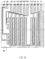
- la figure 6 montre le dessin des électrodes et des connexions pour un dispositif comportant une matrice de 10 lignes et 16 colonnes.
- Les figures 1.a et 1.b représentent le dispositif tel que décrit dans le brevet suisse précité No 633 902. Des volets V1 à V4 sont susceptibles de tourner au-dessus d'une cavité 3, réalisée dans un substrat 5, lorsqu'ils sont soumis à un champ électrique E. Le champ électrique est créé par l'application d'une tension entre une électrode commune 6, placée sur une plaque de verre 8, et l'électrode 7 placée sous le volet. Lorsque la tension entre ces deux électrodes est annulée, le volet qui était adressé revient dans sa position de repos, c'est-à-dire parallèle au plan du substrat, sous l'action des attaches élastiques 4 qui le rattachent au substrat. Il est clair que, dans l'application décrite, la commande des volets ne peut pas être de type matriciel.
- Le dispositif montré à la figure 2, qui fait l'objet du brevet suisse également précité No 641 315 mentionné ci-dessus, est agencé de manière à permettre une commande matricielle des volets. Pour cela les volets V sont arrangés par paires et peuvent être maintenus dans un état actif, c'est-à-dire dans une position orthogonale par rapport au plan du substrat 1, par l'application d'une tension suffisante entre les volets d'une même paire. Dans ce but, les volets comportent au moins une couche conductrice reliée à une électrode de maintien a1, b1, a2 ou b2. Les électrodes c1 à c4 servent, conjointement avec les électrodes ai et bi, à créer le champ électrique d'adressage des volets. Comme indiqué précédemment, il faut éviter que les couches conductrices des volets puissent venir en contact l'une de l'autre lorsque les volets sont activés; ce qui requiert la mise en oeuvre de moyens d'arrêt particuliers décrits dans ledit brevet.
- Le dispositif de l'invention se caractérise par un agencement particulier des électrodes qui permet l'obtention de deux positions stables des volets; à savoir la position de repos et la position activée. Cela est rendu possible grâce à une électrode, dite de maintien et commune à tous les volets, qui stabilise les volets, rendus actifs par l'application de tensions appropriées sur les électrodes de ligne et de colonne correspondantes. La position de repos, quant à elle, est assurée par les électrodes de ligne d'une part et par des moyens mécaniques d'autre part. Il devient alors possible de réaliser une commande matricielle puisque les volets présentent deux positions stables indépendantes des tensions d'adressage. La figure 3 montre schématiquement la position des volets ainsi que la disposition des électrodes qui interviennent tant pour l'adressage de ces derniers que pour leur maintien dans l'une et l'autre des positions stables. La figure 4 montre le détail d'une cellule ainsi que les positions respectives des volets dans les différentes phases d'adressage. La matrice représentée à la figure 3 comprend 10 x 16 cellules réparties en 10 lignes (L01 à L10) et 16 colonnes (C01 à C16). Chaque cellule comprend deux volets disposés côte à côte, comme représenté à la figure 4. Les volets Vaij et Vbij (où "i" représente le numéro de la ligne et "j" le numéro de la colonne), de forme rectangulaire, sont fixés à un substrat 100 par des attaches 10, 20, suffisamment élastiques pour permettre la rotation des volets tout en exerçant sur ces derniers une force de rappel vers la position de repos. Une cavité 110 a été ménagée dans le substrat pour assurer le libre mouvement des volets. Les attaches des volets sont légèrement décentrées vers le substrat et la rotation de ces derniers se fait en sens inverse. Séparée du substrat 100 et fixée à ce dernier par des moyens appropriés, une plaque transparente 30, par exemple en verre, porte des électrodes dites de colonne, telle Cj, et une électrode M dite de maintien. Comme on peut le voir sur les figures 3 et 4, les électrodes de colonne sont disposées au-dessus des colonnes de cellules, respectivement, sans les recouvrir complètement tandis que l'électrode de maintien M est commune à toutes les cellules et est disposée, au niveau de chaque cellule, de part et d'autre de l'électrode de colonne. Les volets, eux-mêmes, constituent des électrodes qui sont toutes reliées à une électrode commune G. Enfin, les électrodes de ligne, L01 à L10, sont disposées sur le substrat, chacune de part et d'autre des cellules de la ligne.
- Le fonctionnement du dispositif de l'invention va maintenant être expliqué en référence à la figure 5 qui montre une séquence d'adressage pour les cellules de la matrice de la figure 3. Au début de la séquence, c'est-à-dire au temps to, les électrodes de ligne L01 à L10 sont toutes activées, par les tensions VL01 à VL10 respectivement, et une tension de maintien VM est appliquée à l'électrode M de maintien. Les volets de toutes les cellules sont alors maintenus dans leur position de repos (position 1, figure 4) par le champ électrique créé entre les électrodes de ligne et les volets; l'électrode G étant toujours reliée à la masse. Les lignes L01 à L10 sont ensuite adressées en succession, pendant les temps t1 à t10 respectivement, en ramenant leur tension à zéro (ou à une tension voisine de zéro). Pendant le temps d'adressage d'une ligne, par exemple le temps t2 pour la ligne L02, les électrodes des colonnes correspondant aux cellules à activer, soit les colonnes C01 et C03, reçoivent une tension de commande VC01, respectivement VC03; ce qui entraîne la rotation des volets correspondants jusqu'à la position 2. Lorsque la tension appliquée sur les électrodes de colonne est ramenée à zéro, soit à la fin du temps d'activation des colonnes, les volets passent de la position 2 à la position 3 sous l'effet du champ créé par l'électrode de maintien sur lesdits volets. A la fin de la séquence d'adressage, la tension VM appliquée à l'électrode M de maintien est, soit maintenue si les volets doivent garder les mêmes positions, soit ramenée à zéro pour que tous les volets reviennent à leur position de repos avant une nouvelle séquence d'adressage.
- La disposition des volets et des électrodes permet la réalisation d'une commande matricielle, indispensable pour des applications exigeant un grand nombre de cellules. La figure 6 montre un exemple des électrodes de colonne et de maintien réalisées sur une plaque transparente (plaque 30 dans la figure 4), pour la matrice de cellules de la figure 3. Sont également représentées sur cette figure 6 les connexions des électrodes de ligne et de l'électrode de masse (électrode G reliée aux volets). Ces dernières connexions peuvent être reliées aux électrodes correspondantes sur le substrat au moyen d'entretoises conductrices. Bien entendu, les électrodes réalisées sur la plaque transparente doivent elles-mêmes être transparentes, ce qui peut être obtenu avec un oxyde d'étain et d'indium, appelé ITO.
- On comprend que les positions et les dimensions des électrodes de colonne et de maintien ainsi que les valeurs des tensions qui leur sont appliquées déterminent les positions prises par les volets lorsqu'ils sont adressés, respectivement maintenus. En fait, les dimensions des différents éléments dépendent de l'application envisagée. A titre d'exemple non limitatif, a été réalisé un dispositif de modulation de lumière comportant une matrice de 10 x 16 cellules, dont les caractéristiques sont les suivantes:
Dimensions de la matrice: 19 mm x 30 mm.
Dimensions des volets: 550 µm x 1 100 µm.
Tension de ligne: 20 volts.
Tension de colonne: 30 volts.
Tension de maintien: 25 volts.
Espace entre le support et la plaque transparente: 400 µm.
Durée d'une impulsion de commande: 25 ms.
Durée d'une séquence d'adressage: 250 ms. - Différents procédés connus peuvent être utilisés pour la préparation du substrat 100 et la réalisation des volets, de leurs attaches et des électrodes. Un procédé basé sur les techniques d'usinage du silicium a été décrit dans les brevets suisses précités. Un autre procédé, basé sur l'utilisation d'une grille de support métallique, a été décrit dans le brevet suisse No 654 686, délivré le 28 février 1986 et intitulé: "Procédé de fabrication d'un dispositif à microvolets". Les techniques utilisées dans les procédés mentionnés ci-dessus sont parfaitement applicables à la réalisation de la présente invention.
- Bien que l'invention ait été décrite dans le cadre d'un exemple de réalisation particulier, il est clair qu'elle est susceptible de modifications ou de variantes sans sortir de son cadre. Il est, par exemple, possible d'échanger les positions respectives des électrodes de colonne et de maintien et de réaliser les volets de manière qu'ils tournent en sens inverse de celui décrit à la figure 4. Une autre variante consiste à ne prévoir qu'un seul volet par cellule. Par ailleurs selon l'application envisagée, le fond des cavités sous les volets peut être recouvert d'un matériau absorbant ou réfléchissant la lumière ou encore être transparent; les surfaces externes des volets peuvent être réfléchissantes ou diffusantes.
Claims (4)
- Dispositif de modulation de lumière à adressage matriciel comportant une matrice de cellules, chaque cellule comprenant un ou plusieurs volets (Vaij, Vbij) qui sont fixés à un substrat (100) par des attaches élastiques (10, 20) et sont susceptibles de tourner autour de leurs attaches sous l'action d'un champ électrique, des électrodes de ligne (L01 - L10) réalisées sur ledit substrat et des électrodes de colonne (C01 - C16) portées par une plaque transparente (30) disposée à distance fixe dudit substrat; ledit dispositif étant caractérisé en ce que:- lesdits volets portent des électrodes qui sont reliées entre elles ainsi qu'à une tension de référence (VG);- lesdites électrodes de ligne, réalisées sur ledit substrat, sont disposées dans l'alignement desdits volets de manière à maintenir ceux-ci en position de repos (1) lorsqu'ils ne sont pas adressés, grâce à l'application d'une différence de tension (VLi) entre les volets et lesdites électrodes de ligne;- lesdites électrodes de colonne sont disposées au-dessus des volets de telle manière qu'elles puissent, sous l'action d'une tension de commande (VCi) appliquée auxdites électrodes de colonne, entraîner la rotation des volets lorsqu'ils sont adressés;- une électrode de maintien (M) commune à tous les volets est prévue sur ladite plaque transparente et reçoit une tension de maintien (VM) propre à maintenir les volets qui ont été adressés en position active (3) lorsque la tension de commande disparait.
- Dispositif de modulation de lumière selon la revendication 1, caractérisé en ce que lesdites électrodes de ligne sont successivement adressées en amenant leur tension à une valeur sensiblement égale à ladite tension de référence et en ce qu'à chaque période d'adressage d'une ligne, les électrodes de colonne qui correspondent aux volets de la ligne à commander, reçoivent simultanément ladite tension de commande pendant le temps d'adressage de la ligne.
- Dispositif selon la revendication 1, caractérisé en ce que chaque cellule comprend deux volets et en ce que l'axe de rotation de chaque volet est distinct de son axe de symétrie.
- Dispositif selon la revendication 3, caractérisé en ce que ladite électrode de maintien est, au niveau de chaque cellule, disposée de part et d'autre de l'électrode de colonne.
Applications Claiming Priority (2)
| Application Number | Priority Date | Filing Date | Title |
|---|---|---|---|
| CH1337/90 | 1990-04-20 | ||
| CH1337/90A CH682523A5 (fr) | 1990-04-20 | 1990-04-20 | Dispositif de modulation de lumière à adressage matriciel. |
Publications (2)
| Publication Number | Publication Date |
|---|---|
| EP0453400A1 EP0453400A1 (fr) | 1991-10-23 |
| EP0453400B1 true EP0453400B1 (fr) | 1994-07-20 |
Family
ID=4208121
Family Applications (1)
| Application Number | Title | Priority Date | Filing Date |
|---|---|---|---|
| EP91810254A Expired - Lifetime EP0453400B1 (fr) | 1990-04-20 | 1991-04-05 | Dispositif de modulation de lumière à adressage matriciel |
Country Status (7)
| Country | Link |
|---|---|
| US (1) | US5078479A (fr) |
| EP (1) | EP0453400B1 (fr) |
| JP (1) | JPH04230721A (fr) |
| AT (1) | ATE108932T1 (fr) |
| CH (1) | CH682523A5 (fr) |
| DE (1) | DE69102933T2 (fr) |
| DK (1) | DK0453400T3 (fr) |
Families Citing this family (278)
| Publication number | Priority date | Publication date | Assignee | Title |
|---|---|---|---|---|
| US5835255A (en) * | 1986-04-23 | 1998-11-10 | Etalon, Inc. | Visible spectrum modulator arrays |
| US5408253A (en) * | 1992-08-03 | 1995-04-18 | Eastman Kodak Company | Integrated galvanometer scanning device |
| US5285196A (en) * | 1992-10-15 | 1994-02-08 | Texas Instruments Incorporated | Bistable DMD addressing method |
| US6674562B1 (en) | 1994-05-05 | 2004-01-06 | Iridigm Display Corporation | Interferometric modulation of radiation |
| US5455709A (en) * | 1993-03-23 | 1995-10-03 | Martin Marietta Corporation | Total internal reflection spatial light modulation apparatus and method of fabrication thereof |
| US5552925A (en) * | 1993-09-07 | 1996-09-03 | John M. Baker | Electro-micro-mechanical shutters on transparent substrates |
| FR2710161B1 (fr) * | 1993-09-13 | 1995-11-24 | Suisse Electronique Microtech | Réseau miniature d'obturateurs de lumière. |
| US7123216B1 (en) | 1994-05-05 | 2006-10-17 | Idc, Llc | Photonic MEMS and structures |
| US7550794B2 (en) * | 2002-09-20 | 2009-06-23 | Idc, Llc | Micromechanical systems device comprising a displaceable electrode and a charge-trapping layer |
| US6040937A (en) * | 1994-05-05 | 2000-03-21 | Etalon, Inc. | Interferometric modulation |
| US7776631B2 (en) | 1994-05-05 | 2010-08-17 | Qualcomm Mems Technologies, Inc. | MEMS device and method of forming a MEMS device |
| US7138984B1 (en) | 2001-06-05 | 2006-11-21 | Idc, Llc | Directly laminated touch sensitive screen |
| US6680792B2 (en) * | 1994-05-05 | 2004-01-20 | Iridigm Display Corporation | Interferometric modulation of radiation |
| US6710908B2 (en) | 1994-05-05 | 2004-03-23 | Iridigm Display Corporation | Controlling micro-electro-mechanical cavities |
| US8014059B2 (en) * | 1994-05-05 | 2011-09-06 | Qualcomm Mems Technologies, Inc. | System and method for charge control in a MEMS device |
| US7297471B1 (en) | 2003-04-15 | 2007-11-20 | Idc, Llc | Method for manufacturing an array of interferometric modulators |
| US7460291B2 (en) | 1994-05-05 | 2008-12-02 | Idc, Llc | Separable modulator |
| US20010003487A1 (en) * | 1996-11-05 | 2001-06-14 | Mark W. Miles | Visible spectrum modulator arrays |
| JP3311194B2 (ja) * | 1995-02-24 | 2002-08-05 | 旭光学工業株式会社 | 光位相変調素子 |
| US5784190A (en) * | 1995-04-27 | 1998-07-21 | John M. Baker | Electro-micro-mechanical shutters on transparent substrates |
| US6046840A (en) | 1995-06-19 | 2000-04-04 | Reflectivity, Inc. | Double substrate reflective spatial light modulator with self-limiting micro-mechanical elements |
| US5835256A (en) * | 1995-06-19 | 1998-11-10 | Reflectivity, Inc. | Reflective spatial light modulator with encapsulated micro-mechanical elements |
| US5757536A (en) * | 1995-08-30 | 1998-05-26 | Sandia Corporation | Electrically-programmable diffraction grating |
| US7907319B2 (en) * | 1995-11-06 | 2011-03-15 | Qualcomm Mems Technologies, Inc. | Method and device for modulating light with optical compensation |
| US5781333A (en) * | 1996-08-20 | 1998-07-14 | Lanzillotta; John | Piezoelectric light shutter |
| US7471444B2 (en) * | 1996-12-19 | 2008-12-30 | Idc, Llc | Interferometric modulation of radiation |
| US5844711A (en) * | 1997-01-10 | 1998-12-01 | Northrop Grumman Corporation | Tunable spatial light modulator |
| WO1998038801A1 (fr) * | 1997-02-26 | 1998-09-03 | Daewoo Electronics Co., Ltd. | Groupement de miroirs actionnes, a couche mince, utilise dans un systeme de projection optique et son procede de fabrication |
| US5815305A (en) * | 1997-03-10 | 1998-09-29 | Daewoo Electronics Co., Ltd. | Thin film actuated mirror array in an optical projection system and method for manufacturing the same |
| US6201629B1 (en) | 1997-08-27 | 2001-03-13 | Microoptical Corporation | Torsional micro-mechanical mirror system |
| US7532377B2 (en) | 1998-04-08 | 2009-05-12 | Idc, Llc | Movable micro-electromechanical device |
| US8928967B2 (en) | 1998-04-08 | 2015-01-06 | Qualcomm Mems Technologies, Inc. | Method and device for modulating light |
| WO1999052006A2 (fr) * | 1998-04-08 | 1999-10-14 | Etalon, Inc. | Modulation interferometrique de rayonnement |
| US6529310B1 (en) | 1998-09-24 | 2003-03-04 | Reflectivity, Inc. | Deflectable spatial light modulator having superimposed hinge and deflectable element |
| JP3919954B2 (ja) * | 1998-10-16 | 2007-05-30 | 富士フイルム株式会社 | アレイ型光変調素子及び平面ディスプレイの駆動方法 |
| US6201633B1 (en) | 1999-06-07 | 2001-03-13 | Xerox Corporation | Micro-electromechanical based bistable color display sheets |
| US8023724B2 (en) * | 1999-07-22 | 2011-09-20 | Photon-X, Inc. | Apparatus and method of information extraction from electromagnetic energy based upon multi-characteristic spatial geometry processing |
| WO2003007049A1 (fr) | 1999-10-05 | 2003-01-23 | Iridigm Display Corporation | Mems et structures photoniques |
| US6396619B1 (en) | 2000-01-28 | 2002-05-28 | Reflectivity, Inc. | Deflectable spatial light modulator having stopping mechanisms |
| US6741383B2 (en) | 2000-08-11 | 2004-05-25 | Reflectivity, Inc. | Deflectable micromirrors with stopping mechanisms |
| US7099065B2 (en) * | 2000-08-03 | 2006-08-29 | Reflectivity, Inc. | Micromirrors with OFF-angle electrodes and stops |
| US6962771B1 (en) * | 2000-10-13 | 2005-11-08 | Taiwan Semiconductor Manufacturing Company, Ltd. | Dual damascene process |
| US7116862B1 (en) | 2000-12-22 | 2006-10-03 | Cheetah Omni, Llc | Apparatus and method for providing gain equalization |
| US6445502B1 (en) | 2001-02-02 | 2002-09-03 | Celeste Optics, Inc. | Variable blazed grating |
| US6721473B1 (en) | 2001-02-02 | 2004-04-13 | Cheetah Omni, Llc | Variable blazed grating based signal processing |
| US7339714B1 (en) | 2001-02-02 | 2008-03-04 | Cheetah Omni, Llc | Variable blazed grating based signal processing |
| US7145704B1 (en) * | 2003-11-25 | 2006-12-05 | Cheetah Omni, Llc | Optical logic gate based optical router |
| FR2822282B1 (fr) * | 2001-03-16 | 2003-07-04 | Information Technology Dev | Ecran plat a valves de lumiere |
| US6589625B1 (en) | 2001-08-01 | 2003-07-08 | Iridigm Display Corporation | Hermetic seal and method to create the same |
| US7110671B1 (en) * | 2001-12-03 | 2006-09-19 | Cheetah Omni, Llc | Method and apparatus for scheduling communication using a star switching fabric |
| US20030107794A1 (en) * | 2001-12-11 | 2003-06-12 | Siekkinen James W. | Micro mirror array |
| US6794119B2 (en) * | 2002-02-12 | 2004-09-21 | Iridigm Display Corporation | Method for fabricating a structure for a microelectromechanical systems (MEMS) device |
| US6574033B1 (en) | 2002-02-27 | 2003-06-03 | Iridigm Display Corporation | Microelectromechanical systems device and method for fabricating same |
| US7781850B2 (en) * | 2002-09-20 | 2010-08-24 | Qualcomm Mems Technologies, Inc. | Controlling electromechanical behavior of structures within a microelectromechanical systems device |
| US7405860B2 (en) * | 2002-11-26 | 2008-07-29 | Texas Instruments Incorporated | Spatial light modulators with light blocking/absorbing areas |
| TW200413810A (en) | 2003-01-29 | 2004-08-01 | Prime View Int Co Ltd | Light interference display panel and its manufacturing method |
| US7417782B2 (en) * | 2005-02-23 | 2008-08-26 | Pixtronix, Incorporated | Methods and apparatus for spatial light modulation |
| TW594360B (en) * | 2003-04-21 | 2004-06-21 | Prime View Int Corp Ltd | A method for fabricating an interference display cell |
| TW570896B (en) | 2003-05-26 | 2004-01-11 | Prime View Int Co Ltd | A method for fabricating an interference display cell |
| US7221495B2 (en) * | 2003-06-24 | 2007-05-22 | Idc Llc | Thin film precursor stack for MEMS manufacturing |
| US7212359B2 (en) * | 2003-07-25 | 2007-05-01 | Texas Instruments Incorporated | Color rendering of illumination light in display systems |
| US7131762B2 (en) * | 2003-07-25 | 2006-11-07 | Texas Instruments Incorporated | Color rendering of illumination light in display systems |
| TW200506479A (en) * | 2003-08-15 | 2005-02-16 | Prime View Int Co Ltd | Color changeable pixel for an interference display |
| TWI231865B (en) * | 2003-08-26 | 2005-05-01 | Prime View Int Co Ltd | An interference display cell and fabrication method thereof |
| TWI232333B (en) * | 2003-09-03 | 2005-05-11 | Prime View Int Co Ltd | Display unit using interferometric modulation and manufacturing method thereof |
| TW593126B (en) | 2003-09-30 | 2004-06-21 | Prime View Int Co Ltd | A structure of a micro electro mechanical system and manufacturing the same |
| US7012726B1 (en) | 2003-11-03 | 2006-03-14 | Idc, Llc | MEMS devices with unreleased thin film components |
| US7142346B2 (en) * | 2003-12-09 | 2006-11-28 | Idc, Llc | System and method for addressing a MEMS display |
| US7161728B2 (en) | 2003-12-09 | 2007-01-09 | Idc, Llc | Area array modulation and lead reduction in interferometric modulators |
| US7532194B2 (en) * | 2004-02-03 | 2009-05-12 | Idc, Llc | Driver voltage adjuster |
| US7119945B2 (en) * | 2004-03-03 | 2006-10-10 | Idc, Llc | Altering temporal response of microelectromechanical elements |
| US7706050B2 (en) * | 2004-03-05 | 2010-04-27 | Qualcomm Mems Technologies, Inc. | Integrated modulator illumination |
| US7476327B2 (en) * | 2004-05-04 | 2009-01-13 | Idc, Llc | Method of manufacture for microelectromechanical devices |
| US7060895B2 (en) | 2004-05-04 | 2006-06-13 | Idc, Llc | Modifying the electro-mechanical behavior of devices |
| US7057786B2 (en) * | 2004-05-10 | 2006-06-06 | Ciencia, Inc. | Electro-optic array interface |
| US6982819B2 (en) * | 2004-05-10 | 2006-01-03 | Ciencia, Inc. | Electro-optic array interface |
| US7164520B2 (en) * | 2004-05-12 | 2007-01-16 | Idc, Llc | Packaging for an interferometric modulator |
| US7787170B2 (en) | 2004-06-15 | 2010-08-31 | Texas Instruments Incorporated | Micromirror array assembly with in-array pillars |
| US7113322B2 (en) * | 2004-06-23 | 2006-09-26 | Reflectivity, Inc | Micromirror having offset addressing electrode |
| US7256922B2 (en) * | 2004-07-02 | 2007-08-14 | Idc, Llc | Interferometric modulators with thin film transistors |
| TWI233916B (en) * | 2004-07-09 | 2005-06-11 | Prime View Int Co Ltd | A structure of a micro electro mechanical system |
| KR101255691B1 (ko) * | 2004-07-29 | 2013-04-17 | 퀄컴 엠이엠에스 테크놀로지스, 인크. | 간섭 변조기의 미소기전 동작을 위한 시스템 및 방법 |
| US7560299B2 (en) * | 2004-08-27 | 2009-07-14 | Idc, Llc | Systems and methods of actuating MEMS display elements |
| US7889163B2 (en) | 2004-08-27 | 2011-02-15 | Qualcomm Mems Technologies, Inc. | Drive method for MEMS devices |
| US7551159B2 (en) * | 2004-08-27 | 2009-06-23 | Idc, Llc | System and method of sensing actuation and release voltages of an interferometric modulator |
| US7499208B2 (en) | 2004-08-27 | 2009-03-03 | Udc, Llc | Current mode display driver circuit realization feature |
| US7515147B2 (en) * | 2004-08-27 | 2009-04-07 | Idc, Llc | Staggered column drive circuit systems and methods |
| US7602375B2 (en) * | 2004-09-27 | 2009-10-13 | Idc, Llc | Method and system for writing data to MEMS display elements |
| US7586484B2 (en) * | 2004-09-27 | 2009-09-08 | Idc, Llc | Controller and driver features for bi-stable display |
| US20060066596A1 (en) * | 2004-09-27 | 2006-03-30 | Sampsell Jeffrey B | System and method of transmitting video data |
| CN100439967C (zh) * | 2004-09-27 | 2008-12-03 | Idc公司 | 用于多状态干涉光调制的方法和设备 |
| US7532195B2 (en) * | 2004-09-27 | 2009-05-12 | Idc, Llc | Method and system for reducing power consumption in a display |
| US7564612B2 (en) * | 2004-09-27 | 2009-07-21 | Idc, Llc | Photonic MEMS and structures |
| US7554714B2 (en) * | 2004-09-27 | 2009-06-30 | Idc, Llc | Device and method for manipulation of thermal response in a modulator |
| US7701631B2 (en) * | 2004-09-27 | 2010-04-20 | Qualcomm Mems Technologies, Inc. | Device having patterned spacers for backplates and method of making the same |
| US7372613B2 (en) | 2004-09-27 | 2008-05-13 | Idc, Llc | Method and device for multistate interferometric light modulation |
| US7310179B2 (en) * | 2004-09-27 | 2007-12-18 | Idc, Llc | Method and device for selective adjustment of hysteresis window |
| US20060176487A1 (en) * | 2004-09-27 | 2006-08-10 | William Cummings | Process control monitors for interferometric modulators |
| US7299681B2 (en) * | 2004-09-27 | 2007-11-27 | Idc, Llc | Method and system for detecting leak in electronic devices |
| US7368803B2 (en) * | 2004-09-27 | 2008-05-06 | Idc, Llc | System and method for protecting microelectromechanical systems array using back-plate with non-flat portion |
| US7553684B2 (en) * | 2004-09-27 | 2009-06-30 | Idc, Llc | Method of fabricating interferometric devices using lift-off processing techniques |
| US7373026B2 (en) * | 2004-09-27 | 2008-05-13 | Idc, Llc | MEMS device fabricated on a pre-patterned substrate |
| US7719500B2 (en) * | 2004-09-27 | 2010-05-18 | Qualcomm Mems Technologies, Inc. | Reflective display pixels arranged in non-rectangular arrays |
| US7535466B2 (en) * | 2004-09-27 | 2009-05-19 | Idc, Llc | System with server based control of client device display features |
| US7936497B2 (en) * | 2004-09-27 | 2011-05-03 | Qualcomm Mems Technologies, Inc. | MEMS device having deformable membrane characterized by mechanical persistence |
| US7369294B2 (en) * | 2004-09-27 | 2008-05-06 | Idc, Llc | Ornamental display device |
| US20060066932A1 (en) * | 2004-09-27 | 2006-03-30 | Clarence Chui | Method of selective etching using etch stop layer |
| US8008736B2 (en) * | 2004-09-27 | 2011-08-30 | Qualcomm Mems Technologies, Inc. | Analog interferometric modulator device |
| US7136213B2 (en) * | 2004-09-27 | 2006-11-14 | Idc, Llc | Interferometric modulators having charge persistence |
| US7527995B2 (en) * | 2004-09-27 | 2009-05-05 | Qualcomm Mems Technologies, Inc. | Method of making prestructure for MEMS systems |
| US7583429B2 (en) | 2004-09-27 | 2009-09-01 | Idc, Llc | Ornamental display device |
| US7630119B2 (en) * | 2004-09-27 | 2009-12-08 | Qualcomm Mems Technologies, Inc. | Apparatus and method for reducing slippage between structures in an interferometric modulator |
| US20060077126A1 (en) * | 2004-09-27 | 2006-04-13 | Manish Kothari | Apparatus and method for arranging devices into an interconnected array |
| US7545550B2 (en) * | 2004-09-27 | 2009-06-09 | Idc, Llc | Systems and methods of actuating MEMS display elements |
| US7345805B2 (en) * | 2004-09-27 | 2008-03-18 | Idc, Llc | Interferometric modulator array with integrated MEMS electrical switches |
| US8878825B2 (en) * | 2004-09-27 | 2014-11-04 | Qualcomm Mems Technologies, Inc. | System and method for providing a variable refresh rate of an interferometric modulator display |
| US7420728B2 (en) * | 2004-09-27 | 2008-09-02 | Idc, Llc | Methods of fabricating interferometric modulators by selectively removing a material |
| US20060065622A1 (en) * | 2004-09-27 | 2006-03-30 | Floyd Philip D | Method and system for xenon fluoride etching with enhanced efficiency |
| US7304784B2 (en) * | 2004-09-27 | 2007-12-04 | Idc, Llc | Reflective display device having viewable display on both sides |
| US7289259B2 (en) * | 2004-09-27 | 2007-10-30 | Idc, Llc | Conductive bus structure for interferometric modulator array |
| US7808703B2 (en) * | 2004-09-27 | 2010-10-05 | Qualcomm Mems Technologies, Inc. | System and method for implementation of interferometric modulator displays |
| US7446927B2 (en) * | 2004-09-27 | 2008-11-04 | Idc, Llc | MEMS switch with set and latch electrodes |
| US7327510B2 (en) * | 2004-09-27 | 2008-02-05 | Idc, Llc | Process for modifying offset voltage characteristics of an interferometric modulator |
| US7417783B2 (en) * | 2004-09-27 | 2008-08-26 | Idc, Llc | Mirror and mirror layer for optical modulator and method |
| US7653371B2 (en) * | 2004-09-27 | 2010-01-26 | Qualcomm Mems Technologies, Inc. | Selectable capacitance circuit |
| US7453579B2 (en) | 2004-09-27 | 2008-11-18 | Idc, Llc | Measurement of the dynamic characteristics of interferometric modulators |
| US7415186B2 (en) * | 2004-09-27 | 2008-08-19 | Idc, Llc | Methods for visually inspecting interferometric modulators for defects |
| US7710629B2 (en) * | 2004-09-27 | 2010-05-04 | Qualcomm Mems Technologies, Inc. | System and method for display device with reinforcing substance |
| US7321456B2 (en) * | 2004-09-27 | 2008-01-22 | Idc, Llc | Method and device for corner interferometric modulation |
| US7679627B2 (en) * | 2004-09-27 | 2010-03-16 | Qualcomm Mems Technologies, Inc. | Controller and driver features for bi-stable display |
| US20060103643A1 (en) * | 2004-09-27 | 2006-05-18 | Mithran Mathew | Measuring and modeling power consumption in displays |
| US7893919B2 (en) | 2004-09-27 | 2011-02-22 | Qualcomm Mems Technologies, Inc. | Display region architectures |
| US7302157B2 (en) * | 2004-09-27 | 2007-11-27 | Idc, Llc | System and method for multi-level brightness in interferometric modulation |
| US7420725B2 (en) | 2004-09-27 | 2008-09-02 | Idc, Llc | Device having a conductive light absorbing mask and method for fabricating same |
| US7916103B2 (en) * | 2004-09-27 | 2011-03-29 | Qualcomm Mems Technologies, Inc. | System and method for display device with end-of-life phenomena |
| US7130104B2 (en) * | 2004-09-27 | 2006-10-31 | Idc, Llc | Methods and devices for inhibiting tilting of a mirror in an interferometric modulator |
| US7692839B2 (en) * | 2004-09-27 | 2010-04-06 | Qualcomm Mems Technologies, Inc. | System and method of providing MEMS device with anti-stiction coating |
| US7492502B2 (en) * | 2004-09-27 | 2009-02-17 | Idc, Llc | Method of fabricating a free-standing microstructure |
| US7405861B2 (en) * | 2004-09-27 | 2008-07-29 | Idc, Llc | Method and device for protecting interferometric modulators from electrostatic discharge |
| US8310441B2 (en) | 2004-09-27 | 2012-11-13 | Qualcomm Mems Technologies, Inc. | Method and system for writing data to MEMS display elements |
| US20060067650A1 (en) * | 2004-09-27 | 2006-03-30 | Clarence Chui | Method of making a reflective display device using thin film transistor production techniques |
| US7417735B2 (en) * | 2004-09-27 | 2008-08-26 | Idc, Llc | Systems and methods for measuring color and contrast in specular reflective devices |
| US7626581B2 (en) * | 2004-09-27 | 2009-12-01 | Idc, Llc | Device and method for display memory using manipulation of mechanical response |
| US7424198B2 (en) | 2004-09-27 | 2008-09-09 | Idc, Llc | Method and device for packaging a substrate |
| US7460246B2 (en) * | 2004-09-27 | 2008-12-02 | Idc, Llc | Method and system for sensing light using interferometric elements |
| US7843410B2 (en) | 2004-09-27 | 2010-11-30 | Qualcomm Mems Technologies, Inc. | Method and device for electrically programmable display |
| US7684104B2 (en) * | 2004-09-27 | 2010-03-23 | Idc, Llc | MEMS using filler material and method |
| US7724993B2 (en) * | 2004-09-27 | 2010-05-25 | Qualcomm Mems Technologies, Inc. | MEMS switches with deforming membranes |
| US8124434B2 (en) * | 2004-09-27 | 2012-02-28 | Qualcomm Mems Technologies, Inc. | Method and system for packaging a display |
| US7359066B2 (en) * | 2004-09-27 | 2008-04-15 | Idc, Llc | Electro-optical measurement of hysteresis in interferometric modulators |
| US7405924B2 (en) | 2004-09-27 | 2008-07-29 | Idc, Llc | System and method for protecting microelectromechanical systems array using structurally reinforced back-plate |
| US7259449B2 (en) * | 2004-09-27 | 2007-08-21 | Idc, Llc | Method and system for sealing a substrate |
| US7289256B2 (en) * | 2004-09-27 | 2007-10-30 | Idc, Llc | Electrical characterization of interferometric modulators |
| US7944599B2 (en) | 2004-09-27 | 2011-05-17 | Qualcomm Mems Technologies, Inc. | Electromechanical device with optical function separated from mechanical and electrical function |
| US7355780B2 (en) * | 2004-09-27 | 2008-04-08 | Idc, Llc | System and method of illuminating interferometric modulators using backlighting |
| US7161730B2 (en) | 2004-09-27 | 2007-01-09 | Idc, Llc | System and method for providing thermal compensation for an interferometric modulator display |
| US7675669B2 (en) * | 2004-09-27 | 2010-03-09 | Qualcomm Mems Technologies, Inc. | Method and system for driving interferometric modulators |
| US7813026B2 (en) * | 2004-09-27 | 2010-10-12 | Qualcomm Mems Technologies, Inc. | System and method of reducing color shift in a display |
| US7920135B2 (en) * | 2004-09-27 | 2011-04-05 | Qualcomm Mems Technologies, Inc. | Method and system for driving a bi-stable display |
| US7317568B2 (en) * | 2004-09-27 | 2008-01-08 | Idc, Llc | System and method of implementation of interferometric modulators for display mirrors |
| US7349136B2 (en) * | 2004-09-27 | 2008-03-25 | Idc, Llc | Method and device for a display having transparent components integrated therein |
| US20060065366A1 (en) * | 2004-09-27 | 2006-03-30 | Cummings William J | Portable etch chamber |
| US7668415B2 (en) * | 2004-09-27 | 2010-02-23 | Qualcomm Mems Technologies, Inc. | Method and device for providing electronic circuitry on a backplate |
| US7369296B2 (en) * | 2004-09-27 | 2008-05-06 | Idc, Llc | Device and method for modifying actuation voltage thresholds of a deformable membrane in an interferometric modulator |
| US7343080B2 (en) * | 2004-09-27 | 2008-03-11 | Idc, Llc | System and method of testing humidity in a sealed MEMS device |
| US20060076634A1 (en) | 2004-09-27 | 2006-04-13 | Lauren Palmateer | Method and system for packaging MEMS devices with incorporated getter |
| US7092143B2 (en) * | 2004-10-19 | 2006-08-15 | Reflectivity, Inc | Micromirror array device and a method for making the same |
| TW200628877A (en) * | 2005-02-04 | 2006-08-16 | Prime View Int Co Ltd | Method of manufacturing optical interference type color display |
| US20070205969A1 (en) | 2005-02-23 | 2007-09-06 | Pixtronix, Incorporated | Direct-view MEMS display devices and methods for generating images thereon |
| US20060209012A1 (en) * | 2005-02-23 | 2006-09-21 | Pixtronix, Incorporated | Devices having MEMS displays |
| US8519945B2 (en) * | 2006-01-06 | 2013-08-27 | Pixtronix, Inc. | Circuits for controlling display apparatus |
| US8159428B2 (en) | 2005-02-23 | 2012-04-17 | Pixtronix, Inc. | Display methods and apparatus |
| US7502159B2 (en) * | 2005-02-23 | 2009-03-10 | Pixtronix, Inc. | Methods and apparatus for actuating displays |
| US9229222B2 (en) * | 2005-02-23 | 2016-01-05 | Pixtronix, Inc. | Alignment methods in fluid-filled MEMS displays |
| US8482496B2 (en) * | 2006-01-06 | 2013-07-09 | Pixtronix, Inc. | Circuits for controlling MEMS display apparatus on a transparent substrate |
| US8310442B2 (en) | 2005-02-23 | 2012-11-13 | Pixtronix, Inc. | Circuits for controlling display apparatus |
| US9158106B2 (en) * | 2005-02-23 | 2015-10-13 | Pixtronix, Inc. | Display methods and apparatus |
| US9082353B2 (en) | 2010-01-05 | 2015-07-14 | Pixtronix, Inc. | Circuits for controlling display apparatus |
| US9261694B2 (en) * | 2005-02-23 | 2016-02-16 | Pixtronix, Inc. | Display apparatus and methods for manufacture thereof |
| US7999994B2 (en) | 2005-02-23 | 2011-08-16 | Pixtronix, Inc. | Display apparatus and methods for manufacture thereof |
| US7295363B2 (en) | 2005-04-08 | 2007-11-13 | Texas Instruments Incorporated | Optical coating on light transmissive substrates of micromirror devices |
| US7920136B2 (en) * | 2005-05-05 | 2011-04-05 | Qualcomm Mems Technologies, Inc. | System and method of driving a MEMS display device |
| KR20080027236A (ko) | 2005-05-05 | 2008-03-26 | 콸콤 인코포레이티드 | 다이나믹 드라이버 ic 및 디스플레이 패널 구성 |
| US7948457B2 (en) * | 2005-05-05 | 2011-05-24 | Qualcomm Mems Technologies, Inc. | Systems and methods of actuating MEMS display elements |
| US20060277486A1 (en) * | 2005-06-02 | 2006-12-07 | Skinner David N | File or user interface element marking system |
| JP2009503564A (ja) * | 2005-07-22 | 2009-01-29 | クアルコム,インコーポレイテッド | Memsデバイスのための支持構造、およびその方法 |
| EP2495212A3 (fr) * | 2005-07-22 | 2012-10-31 | QUALCOMM MEMS Technologies, Inc. | Dispositifs MEMS comportant des structures de support et procédés de fabrication associés |
| US7355779B2 (en) * | 2005-09-02 | 2008-04-08 | Idc, Llc | Method and system for driving MEMS display elements |
| KR20080068821A (ko) | 2005-09-30 | 2008-07-24 | 퀄컴 엠이엠스 테크놀로지스, 인크. | Mems 장치 및 해당 장치용의 접속부 |
| US7630114B2 (en) * | 2005-10-28 | 2009-12-08 | Idc, Llc | Diffusion barrier layer for MEMS devices |
| US7429983B2 (en) * | 2005-11-01 | 2008-09-30 | Cheetah Omni, Llc | Packet-based digital display system |
| US8391630B2 (en) | 2005-12-22 | 2013-03-05 | Qualcomm Mems Technologies, Inc. | System and method for power reduction when decompressing video streams for interferometric modulator displays |
| US7795061B2 (en) | 2005-12-29 | 2010-09-14 | Qualcomm Mems Technologies, Inc. | Method of creating MEMS device cavities by a non-etching process |
| US7636151B2 (en) * | 2006-01-06 | 2009-12-22 | Qualcomm Mems Technologies, Inc. | System and method for providing residual stress test structures |
| US7916980B2 (en) | 2006-01-13 | 2011-03-29 | Qualcomm Mems Technologies, Inc. | Interconnect structure for MEMS device |
| US7382515B2 (en) * | 2006-01-18 | 2008-06-03 | Qualcomm Mems Technologies, Inc. | Silicon-rich silicon nitrides as etch stops in MEMS manufacture |
| US7652814B2 (en) | 2006-01-27 | 2010-01-26 | Qualcomm Mems Technologies, Inc. | MEMS device with integrated optical element |
| US8194056B2 (en) * | 2006-02-09 | 2012-06-05 | Qualcomm Mems Technologies Inc. | Method and system for writing data to MEMS display elements |
| US7582952B2 (en) * | 2006-02-21 | 2009-09-01 | Qualcomm Mems Technologies, Inc. | Method for providing and removing discharging interconnect for chip-on-glass output leads and structures thereof |
| US7547568B2 (en) * | 2006-02-22 | 2009-06-16 | Qualcomm Mems Technologies, Inc. | Electrical conditioning of MEMS device and insulating layer thereof |
| US8526096B2 (en) | 2006-02-23 | 2013-09-03 | Pixtronix, Inc. | Mechanical light modulators with stressed beams |
| US7550810B2 (en) * | 2006-02-23 | 2009-06-23 | Qualcomm Mems Technologies, Inc. | MEMS device having a layer movable at asymmetric rates |
| US7450295B2 (en) * | 2006-03-02 | 2008-11-11 | Qualcomm Mems Technologies, Inc. | Methods for producing MEMS with protective coatings using multi-component sacrificial layers |
| US7643203B2 (en) * | 2006-04-10 | 2010-01-05 | Qualcomm Mems Technologies, Inc. | Interferometric optical display system with broadband characteristics |
| US7903047B2 (en) * | 2006-04-17 | 2011-03-08 | Qualcomm Mems Technologies, Inc. | Mode indicator for interferometric modulator displays |
| US7623287B2 (en) * | 2006-04-19 | 2009-11-24 | Qualcomm Mems Technologies, Inc. | Non-planar surface structures and process for microelectromechanical systems |
| US7711239B2 (en) | 2006-04-19 | 2010-05-04 | Qualcomm Mems Technologies, Inc. | Microelectromechanical device and method utilizing nanoparticles |
| US7417784B2 (en) * | 2006-04-19 | 2008-08-26 | Qualcomm Mems Technologies, Inc. | Microelectromechanical device and method utilizing a porous surface |
| US7527996B2 (en) * | 2006-04-19 | 2009-05-05 | Qualcomm Mems Technologies, Inc. | Non-planar surface structures and process for microelectromechanical systems |
| US20070249078A1 (en) * | 2006-04-19 | 2007-10-25 | Ming-Hau Tung | Non-planar surface structures and process for microelectromechanical systems |
| US8049713B2 (en) * | 2006-04-24 | 2011-11-01 | Qualcomm Mems Technologies, Inc. | Power consumption optimized display update |
| US7369292B2 (en) * | 2006-05-03 | 2008-05-06 | Qualcomm Mems Technologies, Inc. | Electrode and interconnect materials for MEMS devices |
| US7649671B2 (en) * | 2006-06-01 | 2010-01-19 | Qualcomm Mems Technologies, Inc. | Analog interferometric modulator device with electrostatic actuation and release |
| US7321457B2 (en) | 2006-06-01 | 2008-01-22 | Qualcomm Incorporated | Process and structure for fabrication of MEMS device having isolated edge posts |
| US7405863B2 (en) * | 2006-06-01 | 2008-07-29 | Qualcomm Mems Technologies, Inc. | Patterning of mechanical layer in MEMS to reduce stresses at supports |
| US7471442B2 (en) * | 2006-06-15 | 2008-12-30 | Qualcomm Mems Technologies, Inc. | Method and apparatus for low range bit depth enhancements for MEMS display architectures |
| US7702192B2 (en) | 2006-06-21 | 2010-04-20 | Qualcomm Mems Technologies, Inc. | Systems and methods for driving MEMS display |
| US7835061B2 (en) * | 2006-06-28 | 2010-11-16 | Qualcomm Mems Technologies, Inc. | Support structures for free-standing electromechanical devices |
| US7385744B2 (en) * | 2006-06-28 | 2008-06-10 | Qualcomm Mems Technologies, Inc. | Support structure for free-standing MEMS device and methods for forming the same |
| US7777715B2 (en) | 2006-06-29 | 2010-08-17 | Qualcomm Mems Technologies, Inc. | Passive circuits for de-multiplexing display inputs |
| US7388704B2 (en) * | 2006-06-30 | 2008-06-17 | Qualcomm Mems Technologies, Inc. | Determination of interferometric modulator mirror curvature and airgap variation using digital photographs |
| US7527998B2 (en) | 2006-06-30 | 2009-05-05 | Qualcomm Mems Technologies, Inc. | Method of manufacturing MEMS devices providing air gap control |
| US7566664B2 (en) * | 2006-08-02 | 2009-07-28 | Qualcomm Mems Technologies, Inc. | Selective etching of MEMS using gaseous halides and reactive co-etchants |
| US7763546B2 (en) | 2006-08-02 | 2010-07-27 | Qualcomm Mems Technologies, Inc. | Methods for reducing surface charges during the manufacture of microelectromechanical systems devices |
| US20080043315A1 (en) * | 2006-08-15 | 2008-02-21 | Cummings William J | High profile contacts for microelectromechanical systems |
| US7706042B2 (en) * | 2006-12-20 | 2010-04-27 | Qualcomm Mems Technologies, Inc. | MEMS device and interconnects for same |
| US7535621B2 (en) | 2006-12-27 | 2009-05-19 | Qualcomm Mems Technologies, Inc. | Aluminum fluoride films for microelectromechanical system applications |
| US9176318B2 (en) * | 2007-05-18 | 2015-11-03 | Pixtronix, Inc. | Methods for manufacturing fluid-filled MEMS displays |
| US7733552B2 (en) * | 2007-03-21 | 2010-06-08 | Qualcomm Mems Technologies, Inc | MEMS cavity-coating layers and methods |
| US7719752B2 (en) | 2007-05-11 | 2010-05-18 | Qualcomm Mems Technologies, Inc. | MEMS structures, methods of fabricating MEMS components on separate substrates and assembly of same |
| US7570415B2 (en) * | 2007-08-07 | 2009-08-04 | Qualcomm Mems Technologies, Inc. | MEMS device and interconnects for same |
| US7684101B2 (en) * | 2007-10-11 | 2010-03-23 | Eastman Kodak Company | Micro-electromechanical microshutter array |
| US8087811B2 (en) * | 2007-12-19 | 2012-01-03 | Edward Pakhchyan | Display |
| US8177406B2 (en) * | 2007-12-19 | 2012-05-15 | Edward Pakhchyan | Display including waveguide, micro-prisms and micro-mirrors |
| BRPI0908803A2 (pt) * | 2008-02-11 | 2015-07-21 | Qualcomm Mems Technologie Inc | Dispositivo e método de sensoreamento, mensuração ou caracterização de elementos de tela integrados com o esquema de drive de tela |
| US8248560B2 (en) * | 2008-04-18 | 2012-08-21 | Pixtronix, Inc. | Light guides and backlight systems incorporating prismatic structures and light redirectors |
| US7920317B2 (en) * | 2008-08-04 | 2011-04-05 | Pixtronix, Inc. | Display with controlled formation of bubbles |
| US8169679B2 (en) | 2008-10-27 | 2012-05-01 | Pixtronix, Inc. | MEMS anchors |
| US20110205259A1 (en) * | 2008-10-28 | 2011-08-25 | Pixtronix, Inc. | System and method for selecting display modes |
| US8194178B2 (en) * | 2008-12-19 | 2012-06-05 | Omnivision Technologies, Inc. | Programmable micro-electromechanical microshutter array |
| US8736590B2 (en) * | 2009-03-27 | 2014-05-27 | Qualcomm Mems Technologies, Inc. | Low voltage driver scheme for interferometric modulators |
| US8313226B2 (en) | 2010-05-28 | 2012-11-20 | Edward Pakhchyan | Display including waveguide, micro-prisms and micro-shutters |
| KR20120132680A (ko) | 2010-02-02 | 2012-12-07 | 픽스트로닉스 인코포레이티드 | 저온 실 유체 충전된 디스플레이 장치의 제조 방법 |
| JP2013519122A (ja) | 2010-02-02 | 2013-05-23 | ピクストロニックス・インコーポレーテッド | ディスプレイ装置を制御するための回路 |
| US20110205756A1 (en) * | 2010-02-19 | 2011-08-25 | Pixtronix, Inc. | Light guides and backlight systems incorporating prismatic structures and light redirectors |
| CN102834761A (zh) | 2010-04-09 | 2012-12-19 | 高通Mems科技公司 | 机电装置的机械层及其形成方法 |
| US9134527B2 (en) | 2011-04-04 | 2015-09-15 | Qualcomm Mems Technologies, Inc. | Pixel via and methods of forming the same |
| US8963159B2 (en) | 2011-04-04 | 2015-02-24 | Qualcomm Mems Technologies, Inc. | Pixel via and methods of forming the same |
| US9568713B2 (en) | 2013-01-05 | 2017-02-14 | Light Labs Inc. | Methods and apparatus for using multiple optical chains in parallel to support separate color-capture |
| US9134552B2 (en) | 2013-03-13 | 2015-09-15 | Pixtronix, Inc. | Display apparatus with narrow gap electrostatic actuators |
| US9374514B2 (en) | 2013-10-18 | 2016-06-21 | The Lightco Inc. | Methods and apparatus relating to a camera including multiple optical chains |
| US9551854B2 (en) | 2013-10-18 | 2017-01-24 | Light Labs Inc. | Methods and apparatus for controlling sensors to capture images in a synchronized manner |
| US9325906B2 (en) | 2013-10-18 | 2016-04-26 | The Lightco Inc. | Methods and apparatus relating to a thin camera device |
| US9736365B2 (en) | 2013-10-26 | 2017-08-15 | Light Labs Inc. | Zoom related methods and apparatus |
| US9467627B2 (en) | 2013-10-26 | 2016-10-11 | The Lightco Inc. | Methods and apparatus for use with multiple optical chains |
| US9686471B2 (en) | 2013-11-01 | 2017-06-20 | Light Labs Inc. | Methods and apparatus relating to image stabilization |
| US9554031B2 (en) | 2013-12-31 | 2017-01-24 | Light Labs Inc. | Camera focusing related methods and apparatus |
| US9462170B2 (en) | 2014-02-21 | 2016-10-04 | The Lightco Inc. | Lighting methods and apparatus |
| US9979878B2 (en) | 2014-02-21 | 2018-05-22 | Light Labs Inc. | Intuitive camera user interface methods and apparatus |
| EP3164831A4 (fr) | 2014-07-04 | 2018-02-14 | Light Labs Inc. | Procédés et appareils se rapportant à la détection et/ou l'indication d'un état de lentille sale |
| WO2016007799A1 (fr) | 2014-07-09 | 2016-01-14 | The Lightco Inc. | Dispositif de caméra comprenant de multiples chaînes optiques et procédés associés |
| WO2016061565A1 (fr) | 2014-10-17 | 2016-04-21 | The Lightco Inc. | Procédés et appareil d'utilisation d'un dispositif d'appareil photo afin de prendre en charge de multiples modes de fonctionnement |
| EP3235243A4 (fr) | 2014-12-17 | 2018-06-20 | Light Labs Inc. | Procédés et appareil pour mettre en oeuvre et utiliser des dispositifs d'appareil photographique |
| US9544503B2 (en) | 2014-12-30 | 2017-01-10 | Light Labs Inc. | Exposure control methods and apparatus |
| US9824427B2 (en) | 2015-04-15 | 2017-11-21 | Light Labs Inc. | Methods and apparatus for generating a sharp image |
| US9967535B2 (en) | 2015-04-17 | 2018-05-08 | Light Labs Inc. | Methods and apparatus for reducing noise in images |
| US9857584B2 (en) | 2015-04-17 | 2018-01-02 | Light Labs Inc. | Camera device methods, apparatus and components |
| US10091447B2 (en) | 2015-04-17 | 2018-10-02 | Light Labs Inc. | Methods and apparatus for synchronizing readout of multiple image sensors |
| US10075651B2 (en) | 2015-04-17 | 2018-09-11 | Light Labs Inc. | Methods and apparatus for capturing images using multiple camera modules in an efficient manner |
| US9930233B2 (en) | 2015-04-22 | 2018-03-27 | Light Labs Inc. | Filter mounting methods and apparatus and related camera apparatus |
| US10129483B2 (en) | 2015-06-23 | 2018-11-13 | Light Labs Inc. | Methods and apparatus for implementing zoom using one or more moveable camera modules |
| US10491806B2 (en) | 2015-08-03 | 2019-11-26 | Light Labs Inc. | Camera device control related methods and apparatus |
| US10365480B2 (en) | 2015-08-27 | 2019-07-30 | Light Labs Inc. | Methods and apparatus for implementing and/or using camera devices with one or more light redirection devices |
| US9749549B2 (en) | 2015-10-06 | 2017-08-29 | Light Labs Inc. | Methods and apparatus for facilitating selective blurring of one or more image portions |
| US10225445B2 (en) | 2015-12-18 | 2019-03-05 | Light Labs Inc. | Methods and apparatus for providing a camera lens or viewing point indicator |
| US10003738B2 (en) | 2015-12-18 | 2018-06-19 | Light Labs Inc. | Methods and apparatus for detecting and/or indicating a blocked sensor or camera module |
| US10306218B2 (en) | 2016-03-22 | 2019-05-28 | Light Labs Inc. | Camera calibration apparatus and methods |
| US9948832B2 (en) | 2016-06-22 | 2018-04-17 | Light Labs Inc. | Methods and apparatus for synchronized image capture in a device including optical chains with different orientations |
Family Cites Families (6)
| Publication number | Priority date | Publication date | Assignee | Title |
|---|---|---|---|---|
| CH633902A5 (fr) * | 1980-03-11 | 1982-12-31 | Centre Electron Horloger | Dispositif de modulation de lumiere. |
| CH641315B (fr) * | 1981-07-02 | Centre Electron Horloger | Dispositif d'affichage miniature a volets. | |
| NL8200354A (nl) * | 1982-02-01 | 1983-09-01 | Philips Nv | Passieve weergeefinrichting. |
| CH654686A5 (fr) * | 1983-11-18 | 1986-02-28 | Centre Electron Horloger | Procede de fabrication d'un dispositif a volets miniatures et application d'un tel procede pour l'obtention d'un dispositif de modulation de lumiere. |
| NL8402038A (nl) * | 1984-06-28 | 1986-01-16 | Philips Nv | Elektroskopische beeldweergeefinrichting. |
| NL8402937A (nl) * | 1984-09-27 | 1986-04-16 | Philips Nv | Elektroskopische beeldweergeefinrichting. |
-
1990
- 1990-04-20 CH CH1337/90A patent/CH682523A5/fr not_active IP Right Cessation
-
1991
- 1991-04-05 DE DE69102933T patent/DE69102933T2/de not_active Expired - Fee Related
- 1991-04-05 DK DK91810254.2T patent/DK0453400T3/da not_active Application Discontinuation
- 1991-04-05 EP EP91810254A patent/EP0453400B1/fr not_active Expired - Lifetime
- 1991-04-05 AT AT91810254T patent/ATE108932T1/de not_active IP Right Cessation
- 1991-04-18 US US07/687,129 patent/US5078479A/en not_active Expired - Lifetime
- 1991-04-19 JP JP3088237A patent/JPH04230721A/ja active Pending
Also Published As
| Publication number | Publication date |
|---|---|
| DE69102933D1 (de) | 1994-08-25 |
| JPH04230721A (ja) | 1992-08-19 |
| US5078479A (en) | 1992-01-07 |
| DK0453400T3 (da) | 1994-11-21 |
| CH682523A5 (fr) | 1993-09-30 |
| DE69102933T2 (de) | 1995-02-23 |
| ATE108932T1 (de) | 1994-08-15 |
| EP0453400A1 (fr) | 1991-10-23 |
Similar Documents
| Publication | Publication Date | Title |
|---|---|---|
| EP0453400B1 (fr) | Dispositif de modulation de lumière à adressage matriciel | |
| CA1232450A (fr) | Dispositif d'affichage miniature a volets | |
| CA1144629A (fr) | Dispositif d'affichage miniature | |
| EP0533543B1 (fr) | Commutateur optique et procédé de fabrication de ce commutateur | |
| EP0258130B1 (fr) | Ecran plat électroluminescent | |
| EP0364314B1 (fr) | Procédé de lecture de cellules photosensibles du type comportant deux diodes montées en série avec des sens de conduction opposés | |
| FR3069378B1 (fr) | Dispositif optoelectronique | |
| EP0245147A1 (fr) | Panneau de prise de vue radiologique, et procédé de fabrication | |
| CH654686A5 (fr) | Procede de fabrication d'un dispositif a volets miniatures et application d'un tel procede pour l'obtention d'un dispositif de modulation de lumiere. | |
| CH680322A5 (fr) | ||
| EP0121467A1 (fr) | Microconnecteur à haute densité de contacts | |
| FR3069379A1 (fr) | Dispositif optoelectronique | |
| EP2721598B1 (fr) | Afficheur a cristal liquide a electrodes d'effacement | |
| EP0316221A1 (fr) | Matrice d'éléments photosensibles associant un phototransistor et une capacité de Stockage | |
| EP1518145B1 (fr) | Cellule d affichage, notamment a cristal liquide, ou cellule photovoltaique comprenant des moyens pour sa connexion a un circuit electronique de commande | |
| EP0228317A1 (fr) | Ecran de visualisation électrooptique à transistors de commande | |
| CH628182A5 (fr) | Dispositif de commande, apte a assurer des commutations. | |
| EP0485285A1 (fr) | Dispositif électrooptique bistable, écran comportant un tel dispositif et procédé de mise en oeuvre de cet écran | |
| EP0217844B1 (fr) | Procede de fabrication d'un ecran d'affichage a cristaux liquides et a reseau de diodes | |
| FR2694859A1 (fr) | Imageur à infrarouge. | |
| EP0828413B1 (fr) | Dispositif d'affichage électro-optique et support flexible pour de tels dispositifs servant à l'alimentation de ces dispositifs | |
| FR2827991A1 (fr) | Panneau de visualisation d'images forme d'une matrice de cellules electroluminescentes a effet memoire | |
| WO1999041638A1 (fr) | Cellule electro-optique ou cellule photovoltaïque, et procede de fabrication d'une telle cellule | |
| EP0697636A1 (fr) | Pièce d'horlogerie alimentée par des cellules solaires | |
| EP0948059A1 (fr) | Moyens de positionnement pour un dispositif microélectronique et appareil de prise de vues muni d'un tel dispositif |
Legal Events
| Date | Code | Title | Description |
|---|---|---|---|
| PUAI | Public reference made under article 153(3) epc to a published international application that has entered the european phase |
Free format text: ORIGINAL CODE: 0009012 |
|
| AK | Designated contracting states |
Kind code of ref document: A1 Designated state(s): AT BE CH DE DK ES FR GB GR IT LI LU NL SE |
|
| 17P | Request for examination filed |
Effective date: 19920307 |
|
| 17Q | First examination report despatched |
Effective date: 19930719 |
|
| GRAA | (expected) grant |
Free format text: ORIGINAL CODE: 0009210 |
|
| AK | Designated contracting states |
Kind code of ref document: B1 Designated state(s): AT BE CH DE DK ES FR GB GR IT LI LU NL SE |
|
| PG25 | Lapsed in a contracting state [announced via postgrant information from national office to epo] |
Ref country code: IT Free format text: LAPSE BECAUSE OF FAILURE TO SUBMIT A TRANSLATION OF THE DESCRIPTION OR TO PAY THE FEE WITHIN THE PRESCRIBED TIME-LIMIT;WARNING: LAPSES OF ITALIAN PATENTS WITH EFFECTIVE DATE BEFORE 2007 MAY HAVE OCCURRED AT ANY TIME BEFORE 2007. THE CORRECT EFFECTIVE DATE MAY BE DIFFERENT FROM THE ONE RECORDED. Effective date: 19940720 Ref country code: GR Free format text: LAPSE BECAUSE OF FAILURE TO SUBMIT A TRANSLATION OF THE DESCRIPTION OR TO PAY THE FEE WITHIN THE PRESCRIBED TIME-LIMIT Effective date: 19940720 Ref country code: ES Free format text: THE PATENT HAS BEEN ANNULLED BY A DECISION OF A NATIONAL AUTHORITY Effective date: 19940720 Ref country code: AT Effective date: 19940720 |
|
| REF | Corresponds to: |
Ref document number: 108932 Country of ref document: AT Date of ref document: 19940815 Kind code of ref document: T |
|
| REF | Corresponds to: |
Ref document number: 69102933 Country of ref document: DE Date of ref document: 19940825 |
|
| PG25 | Lapsed in a contracting state [announced via postgrant information from national office to epo] |
Ref country code: SE Effective date: 19941020 |
|
| REG | Reference to a national code |
Ref country code: DK Ref legal event code: T3 |
|
| GBT | Gb: translation of ep patent filed (gb section 77(6)(a)/1977) |
Effective date: 19941028 |
|
| PG25 | Lapsed in a contracting state [announced via postgrant information from national office to epo] |
Ref country code: BE Effective date: 19950430 Ref country code: LU Free format text: LAPSE BECAUSE OF NON-PAYMENT OF DUE FEES Effective date: 19950430 |
|
| PLBE | No opposition filed within time limit |
Free format text: ORIGINAL CODE: 0009261 |
|
| STAA | Information on the status of an ep patent application or granted ep patent |
Free format text: STATUS: NO OPPOSITION FILED WITHIN TIME LIMIT |
|
| 26N | No opposition filed | ||
| BERE | Be: lapsed |
Owner name: S.A. CENTRE SUISSE D'ELECTRONIQUE ET DE MICROTECH Effective date: 19950430 |
|
| REG | Reference to a national code |
Ref country code: CH Ref legal event code: NV Representative=s name: CSEM CENTRE SUISSE D'ELECTRONIQUE ET DE MICROTECHN Ref country code: CH Ref legal event code: PUE Owner name: CENTRE SUISSE D'ELECTRONIQUE ET DE MICROTECHNIQUE |
|
| REG | Reference to a national code |
Ref country code: GB Ref legal event code: IF02 |
|
| REG | Reference to a national code |
Ref country code: GB Ref legal event code: 732E |
|
| REG | Reference to a national code |
Ref country code: FR Ref legal event code: TP |
|
| NLS | Nl: assignments of ep-patents |
Owner name: COLIBRYS S.A. |
|
| REG | Reference to a national code |
Ref country code: CH Ref legal event code: NV Representative=s name: CABINET ROLAND NITHARDT CONSEILS EN PROPRIETE INDU |
|
| REG | Reference to a national code |
Ref country code: CH Ref legal event code: PCAR Free format text: PATENTS & TECHNOLOGY SURVEYS SA;RUE DES TERREAUX 7 CASE POSTALE 2848;2001 NEUCHATEL (CH) |
|
| PGFP | Annual fee paid to national office [announced via postgrant information from national office to epo] |
Ref country code: DK Payment date: 20090415 Year of fee payment: 19 |
|
| PGFP | Annual fee paid to national office [announced via postgrant information from national office to epo] |
Ref country code: NL Payment date: 20090415 Year of fee payment: 19 Ref country code: DE Payment date: 20090422 Year of fee payment: 19 Ref country code: FR Payment date: 20090414 Year of fee payment: 19 |
|
| PGFP | Annual fee paid to national office [announced via postgrant information from national office to epo] |
Ref country code: CH Payment date: 20090417 Year of fee payment: 19 |
|
| PGFP | Annual fee paid to national office [announced via postgrant information from national office to epo] |
Ref country code: GB Payment date: 20090421 Year of fee payment: 19 |
|
| REG | Reference to a national code |
Ref country code: NL Ref legal event code: V1 Effective date: 20101101 |
|
| REG | Reference to a national code |
Ref country code: CH Ref legal event code: PL |
|
| REG | Reference to a national code |
Ref country code: DK Ref legal event code: EBP |
|
| GBPC | Gb: european patent ceased through non-payment of renewal fee |
Effective date: 20100405 |
|
| REG | Reference to a national code |
Ref country code: FR Ref legal event code: ST Effective date: 20101230 |
|
| PG25 | Lapsed in a contracting state [announced via postgrant information from national office to epo] |
Ref country code: NL Free format text: LAPSE BECAUSE OF NON-PAYMENT OF DUE FEES Effective date: 20101101 |
|
| PG25 | Lapsed in a contracting state [announced via postgrant information from national office to epo] |
Ref country code: DE Free format text: LAPSE BECAUSE OF NON-PAYMENT OF DUE FEES Effective date: 20101103 Ref country code: CH Free format text: LAPSE BECAUSE OF NON-PAYMENT OF DUE FEES Effective date: 20100430 Ref country code: LI Free format text: LAPSE BECAUSE OF NON-PAYMENT OF DUE FEES Effective date: 20100430 |
|
| PG25 | Lapsed in a contracting state [announced via postgrant information from national office to epo] |
Ref country code: GB Free format text: LAPSE BECAUSE OF NON-PAYMENT OF DUE FEES Effective date: 20100405 |
|
| PG25 | Lapsed in a contracting state [announced via postgrant information from national office to epo] |
Ref country code: DK Free format text: LAPSE BECAUSE OF NON-PAYMENT OF DUE FEES Effective date: 20100503 |
|
| PG25 | Lapsed in a contracting state [announced via postgrant information from national office to epo] |
Ref country code: FR Free format text: LAPSE BECAUSE OF NON-PAYMENT OF DUE FEES Effective date: 20100430 |