EP0453314B1 - Non-contact portable carrier - Google Patents
Non-contact portable carrier Download PDFInfo
- Publication number
- EP0453314B1 EP0453314B1 EP91303551A EP91303551A EP0453314B1 EP 0453314 B1 EP0453314 B1 EP 0453314B1 EP 91303551 A EP91303551 A EP 91303551A EP 91303551 A EP91303551 A EP 91303551A EP 0453314 B1 EP0453314 B1 EP 0453314B1
- Authority
- EP
- European Patent Office
- Prior art keywords
- power
- portable carrier
- signal
- state
- voltage
- Prior art date
- Legal status (The legal status is an assumption and is not a legal conclusion. Google has not performed a legal analysis and makes no representation as to the accuracy of the status listed.)
- Expired - Lifetime
Links
Images


Classifications
-
- G—PHYSICS
- G06—COMPUTING; CALCULATING OR COUNTING
- G06K—GRAPHICAL DATA READING; PRESENTATION OF DATA; RECORD CARRIERS; HANDLING RECORD CARRIERS
- G06K19/00—Record carriers for use with machines and with at least a part designed to carry digital markings
- G06K19/06—Record carriers for use with machines and with at least a part designed to carry digital markings characterised by the kind of the digital marking, e.g. shape, nature, code
- G06K19/067—Record carriers with conductive marks, printed circuits or semiconductor circuit elements, e.g. credit or identity cards also with resonating or responding marks without active components
- G06K19/07—Record carriers with conductive marks, printed circuits or semiconductor circuit elements, e.g. credit or identity cards also with resonating or responding marks without active components with integrated circuit chips
- G06K19/0701—Record carriers with conductive marks, printed circuits or semiconductor circuit elements, e.g. credit or identity cards also with resonating or responding marks without active components with integrated circuit chips at least one of the integrated circuit chips comprising an arrangement for power management
-
- G—PHYSICS
- G06—COMPUTING; CALCULATING OR COUNTING
- G06K—GRAPHICAL DATA READING; PRESENTATION OF DATA; RECORD CARRIERS; HANDLING RECORD CARRIERS
- G06K19/00—Record carriers for use with machines and with at least a part designed to carry digital markings
- G06K19/06—Record carriers for use with machines and with at least a part designed to carry digital markings characterised by the kind of the digital marking, e.g. shape, nature, code
- G06K19/067—Record carriers with conductive marks, printed circuits or semiconductor circuit elements, e.g. credit or identity cards also with resonating or responding marks without active components
- G06K19/07—Record carriers with conductive marks, printed circuits or semiconductor circuit elements, e.g. credit or identity cards also with resonating or responding marks without active components with integrated circuit chips
- G06K19/0723—Record carriers with conductive marks, printed circuits or semiconductor circuit elements, e.g. credit or identity cards also with resonating or responding marks without active components with integrated circuit chips the record carrier comprising an arrangement for non-contact communication, e.g. wireless communication circuits on transponder cards, non-contact smart cards or RFIDs
-
- G—PHYSICS
- G06—COMPUTING; CALCULATING OR COUNTING
- G06K—GRAPHICAL DATA READING; PRESENTATION OF DATA; RECORD CARRIERS; HANDLING RECORD CARRIERS
- G06K7/00—Methods or arrangements for sensing record carriers, e.g. for reading patterns
- G06K7/10—Methods or arrangements for sensing record carriers, e.g. for reading patterns by electromagnetic radiation, e.g. optical sensing; by corpuscular radiation
- G06K7/10009—Methods or arrangements for sensing record carriers, e.g. for reading patterns by electromagnetic radiation, e.g. optical sensing; by corpuscular radiation sensing by radiation using wavelengths larger than 0.1 mm, e.g. radio-waves or microwaves
- G06K7/10316—Methods or arrangements for sensing record carriers, e.g. for reading patterns by electromagnetic radiation, e.g. optical sensing; by corpuscular radiation sensing by radiation using wavelengths larger than 0.1 mm, e.g. radio-waves or microwaves using at least one antenna particularly designed for interrogating the wireless record carriers
- G06K7/10336—Methods or arrangements for sensing record carriers, e.g. for reading patterns by electromagnetic radiation, e.g. optical sensing; by corpuscular radiation sensing by radiation using wavelengths larger than 0.1 mm, e.g. radio-waves or microwaves using at least one antenna particularly designed for interrogating the wireless record carriers the antenna being of the near field type, inductive coil
Definitions
- the present invention relates to a portable carrier of non-contact type and, more particularly, to a non-contact portable carrier which is supplied with a power voltage through an electromagnetic coupling.
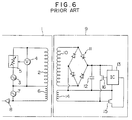
- Fig. 6 shows the construction of a known non-contact portable carrier of electromagnetic coupling type.
- the non-contact portable carrier 9 has a power receiving coil 10 to which is connected a full-wave rectifier circuit 11.
- a smoothing capacitor 12 and an integrating circuit 13 (referred to as "IC" hereinafetr) for controlling and processing signals are connected to the full-wave rectifier circuit 11.
- the smoothing capacitor 11 has a high-voltage terminal and a grounding terminal.
- a signal transmitting/receiving coil 14 is connected to the IC 13 through a received signal detecting element 15 and a signal transmitting element 16.
- the portable carrier 9 thus constructed is set on a terminal device 1.
- the terminal device 1 has a power supplying coil 2 and a signal transmitting/receiving coil 14 which are disposed adjacent the coils 10 and 14 of the portable carrier 9 set on the device 1.
- a power voltage generator 3 and a voltage regulator 5 are connected to the power supplying coil 2.
- a voltage detector 4 for detecting the voltage across the coil 2 is also connected to the power supplying coil 2.
- the output of the voltage detector 4 is connected to the power voltage regulator 5.
- a signal generator 7 and a received signal detecting element 8 are connected to the signal transmitting/receiving coil 6.
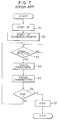
- the operation of the conventional non-contact portable carrier 9 will be described with specific reference to a flow chart shown in Fig. 7.
- the power receiving coil 10 of the portable carrier 9 is brought close to the power supplying coil 12 of the terminal device 1.
- AC voltage is supplied from the power generator 3 to the portable carrier 9 through the power supplying coil 2.
- This AC voltage is rectified into a DC voltage through the full-wave rectifier circuit 11 and the capacitor 12 and thus formed DC voltage is supplied to the IC 13, whereby the portable carrier 9 is started in Step 51 of the flow.
- Step 52 the IC 13 of the portable carrier 9 turns the signal transmitting element 16 on and off, thus delivering to the terminal device 1 a start-up acknowledgment signal indicative of the start-up of the portable carrier 9, through the signal transmitting/receiving coil 14.
- the terminal device 1 Upon detection of the start-up acknowledgment signal through the signal transmitting/receiving coil 6 and the received signal detecting element 8, the terminal device 1 drives the signal generator 7 as necessitated so as to transmit,through the coil 6, a signal indicative of the content of the processing and data.
- Step 53 the portable carrier 9 receives the signal from the terminal device 1 through the coil 14 and the received signal detecting element 15. Upon receipt of this signal, the portable carrier 9 conducts a signal processing operation by means of IC 13. Namely, the portable carrier 9 conducts processing and control of data in accordance with the content of the received signal.
- Step 55 the IC 13 of the portable carrier 9 turns on and off the signal transmitting element 16 as required, so as to deliver a signal indicative of the processing result or data to the terminal device 1 through the signal transmitting/receiving coil 14.
- Step 56 determines that the series of operation is completed.
- Step 56 the process proceeds to Step 57 in which the supply of the AC voltage from the terminal device 1 is ceased so that the operation of the portable carrier 9 is terminated.
- the portable carrier 9 consumes electrical power due to, for example, operation of the IC 13.
- a large power is consumed when the signal transmitting element 16 is turned on and off to deliver a signal to the terminal device 1 through the coil 14.
- the load current in the power supplying coil 2 of the terminal device 1 is increases so that the voltage across this coil 2 is reduced.
- This voltage drop is detected by the voltage detector 4 so that the power voltage regulator 5 operates to increase the voltage across the coil 2 so as to compensate for the voltage drop.
- breakdown of the IC 13 due to instantaneous application of an over-voltage is unavoidable due to delay of response of the voltage detector 4 and the power voltage regulator 5, even when the voltage across the coil 2 is controlled for the purpose of protecting the IC from breakdown.
- the conventional non-contact portable carrier suffers from a problem in that the signal processing means such as an IC tends to be broken down due to application of a high voltage, particularly when the power consumption in the portable carrier is small.
- WO-A-87 06 747 discloses a non-contact portable carrier in the form of a personal memory card.
- This device includes a shunt regulator to regulate the power supplied to the card generally.
- this card does not specifically check for a low voltage condition across the integrated circuit on the card.
- an object of the present invention is to provide a non-contact portable carrier which can prevent breakdown of signal processing means in the carrier even when only small power is being consumed.
- a non-contact portable carrier comprising:
- the non-contact portable carrier has a plurality of the power consuming means having different values of electrical power consumption, which are selectively used under the sequence control of the processing means in accordance with the states of operation of the signal processing means and the signal transmitting/receiving means.
- the rate of consumption of electrical power by the power consuming means is controlled in accordance with the states of operation of the signal processing means and the signal transmitting/receiving means.
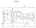
- Fig. 1 is a circuit diagram showing an embodiment of the non-contact portable carrier of the present invention.
- the non-contact portable carrier 90 has a power receiving coil 10 for receiving AC power from a terminal device 1.
- a full-wave rectifier circuit 11 is connected to the coil 10.
- a smoothing capacitor 12 for smoothing pulsating power and an IC 17 for controlling and processing the signals are connected to the full-wave rectifier circuit 11.
- the smoothing capacitor 12 has a high-voltage terminal and a grounding terminal.
- the IC 17 forms a microcomputer and has a built-in sequence-controllable program.
- a signal transmitting/receiving coil 14 is connected to the IC 17 through a received signal detecting element 15 and a signal transmitting element 16.
- a voltage control element 18 is also connected to the IC 17.
- a resistor 19 is connected between the voltage control element 18 and the ground line 20.
- the portable carrier 90 having the described construction is set on a terminal device 1.
- the terminal device 1 has a power supplying coil 2 and a signal transmitting/receiving coil 6 which are positioned adjacent the coil 10and the coil 14 in the portable carrier 90 set on the terminal device 90.
- a power generator 3 and a power voltage regulator 5 are connected to the power supplying coil 2.
- a voltage detector 4 for detecting the voltage across the power supplying coil 2 is also connected to the coil 2. The output of the voltage detector 4 is connected to the power voltage regulator 5.
- a signal generator 7 and a received signal detector 8 are connected to the signal transmitting/receiving coil 6.
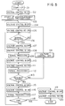
- the power receiving coil 10 of the portable carrier 90 is brought close to the power supplying coil 2 of the terminal device 1, so that an AC voltage is supplied from the power generator 3 to the power receiving coil 10 of the portable carrier 90 through the power supplying coil 2 of the terminal device 1.
- This AC voltage is rectified into a pulsating DC voltage by the full-wave rectifier circuit 11 and the pulsating DC voltage is smoothed by the smoothing capacitor 12, and the smoothed DC voltage is supplied to the IC 17,whereby the portable carrier 90 is started in Step 21.
- Step 22 the IC 17 of the portable carrier 90 turns the signal transmitting element 16 on and off, so as to transmit a start-up acknowledgment signal indicative of the start-up of the portable carrier 90 to the terminal device 1 through the signal transmitting/receiving coil 14.
- the voltage control element 18 is in off state.
- the terminal device 1 detects the start-up acknowledgment signal through the signal transmitting/receiving coil 6 and the received signal detecting element 8 and drives the signal generator 7 as required so as to transmit to the portable carrier 90 a signal indicative of the content of processing and data through the coil 6.
- the portable carrier 90 determines,through the operation of the coil 14 and the received signal detecting element 15, whether the signal has been received from the terminal device 1. When no receipt of signal is detected, the process proceeds to Step 24 in which the voltage supplied to the IC 17 is controlled. When no signal is received, the portable carrier 90 is in a stand-by condition waiting for receipt, so that it consumes only a very small power which is just enough for maintaining electrical current for enabling the IC 17 to hold the data.
- the IC 17 turns the voltage control element 18 on, so that electrical current flows to the ground line 20 through the voltage control element 18 and the resistor 19, thus causing the portable carrier 90 to consume electrical power. As a consequence, abnormal rise of the voltage applied to the IC 17 is prevented.
- Step 23 when receipt of the signal from the terminal device 1 is determined in Step 23, the process proceeds to Step 25 in which the voltage control element 18 is turned off, thereby terminating the control of the voltage supplied to the IC 17, followed by execution of signal processing in Step 26. Namely, processing and control of data are conducted in accordance with the content of the received signal, with a normal power consumption.
- Step 27 the IC 17 of the portable carrier 90 turns on and off the signal transmitting element 16 as required, thereby delivering a signal indicative of the processing result or data to the terminal device 1 through the signal transmitting/receiving coil 14.
- Step 28 whether a series of processing operation has been completed is determined in Step 28. If the operation has not been completed, the process returns to Step 23 to determined whether a signal has been received from the terminal device 1.
- the voltage control is executed in Step 24 to cause the portable carrier to consume electrical power, whereas, when a signal is received, the voltage control is ceased in Step 25 and electrical power is consumed for processing and transmission of signals.
- Step 28 The steps 23 to 27 are repeatedly executed until completion of the series of processing is determined in Step 28.
- the voltage control element 18 is turned on in Step 29 as in Step 24, anticipating the reduction of electrical power consumption in the portable carrier 90, whereby the voltage supplied to the IC 17 is controlled.
- the portable carrier 90 then waits for termination of supply of the AC voltage from the terminal device 1.
- the resistance value of the resistor 19 enabling the portable carrier 90 to consume power is suitably determined in accordance with the rise of the voltage in the stand-by condition and the maximum rating voltage of the IC 17.
- Fig. 3 shows a flow chart illustrative of operation of a second embodiment of the present invention.
- the electrical power consumption by the portable carrier 90 exhibits a peak when the signal transmitting element 16 is turned on and off so as to supply electrical power to the signal transmitting/receiving coil 14 for the purpose of delivering a signal to the terminal device 1.
- the second embodiment is therefore constructed such that the voltage supplied to the IC 17 is always controlled to enable the portable carrier 90 to consume power except the period in which a signal is transmitted to the terminal device 1.
- the second embodiment of the portable carrier is distinguished from the first embodiment only by the content of the program stored in the IC 17.
- the operation of the second embodiment will be described with reference to a flow chart shown in Fig. 3.
- the non-contact portable carrier 90 is set on the terminal device 1
- the portable carrier 90 is started in Step 31 and a start-up acknowledgment signal is transmitted from the portable carrier 90 to the terminal device 1 in Step 32, as in the case of the first embodiment.
- the voltage controlling element 18 is off.
- Step 34 the portable carrier 90 waits for receipt of a signal from the terminal device 1. When the signal is received, the process proceeds to Step 35 in which the IC 17 conducts signal processing.
- Step 36 whether a signal indicative of the processing result or data is to be transmitted to the terminal device 1 is determined in Step 36.
- the process returns to Step 34 in which the portable carrier 90 waits for receipt of a next signal.
- Step 37 is which the voltage controlling element 18 is turned off so as to terminate the control of the voltage supplied to the IC 17.
- the signal transmitting/receiving element 16 is turned on and off so as to transmit a signal to the terminal device 1 through the signal transmitting/receiving coil 14.
- Step 39 whether a series of processing operation has been completed is determined in Step 39. If the series of operation has not been completed yet, Steps 33 to 39 are executed repeatedly. Conversely, when the operation has been finished, the voltage controlling element 18 is turned on in Step 40 as in Step 33 so as to enable control of the voltage supplied to the IC 17. The portable carrier 90 then waits for termination of supply of the AC power from the terminal device 1.
- the IC 17 and the received signal detecting element 15 consume only very small electrical power when operating, particularly when they are constructed as CMOSes.
- the second embodiment, which controls the voltage supplied to the IC 17 to enable the portable carrier 90 to consume power, is specifically effective when the IC 17 and the received signal detecting element 15 are CMOSes devices.
- Fig. 4 is a circuit diagram of a third embodiment of the non-contact portable carrier 91.
- This embodiment incorporates four power consuming means having different power consuming rates.
- the IC 17 as the signal processing means conducts a sequence control so as to conduct a change-over of the electrical power consumption rate in accordance with four states of operation of the non-contact portable carrier, e.g., signal transmitting state, signal receiving state, signal processing state and stand-by state.
- four circuits each having a voltage controlling element and a resistor are connected to the IC 17 in parallel with one another.
- the voltage controlling element 18 When the portable carrier 91 is in the signal transmitting state, the voltage controlling element 18 is turned on so that electrical current is allowed to flow to the ground line 20 through the resistor 19.
- the voltage controlling element 61 When the portable carrier 91 is in the signal receiving state, the voltage controlling element 61 is turned on so that electrical current is allowed to flow to the ground line 20 through the resistor 64.
- the voltage controlling element 62 When the portable carrier 91 is in the signal processing state, the voltage controlling element 62 is turned on so that electrical current is allowed to flow to the ground line 20 through the resistor 65.
- the voltage controlling element 60 When the portable carrier 91 is in the stand-by state, the voltage controlling element 60 is turned on so that electrical current is allowed to flow to the ground line 20 through the resistor 63.
- the resistors 19, 63,64 and 65 have different values of resistance.
- a system having a signal procesing means and signal transmission/receiving means exhibit the smallest power consumption when it is in stand-by state and the power consumption is maximized when the system is in signal transmitting state. It is therefore necessary to select the resistance values of the above-mentioned resistors such that the resistor 60 which is supplied with electrical current when the portable carrier is in the stand-by condition has the smallest resistance value, while the resistor 19 which is supplied with electrical current when the portable carrier 91 is in the signal transmitting state has the greatest resistance value, among the above-mentioned four resistors.
- Other portions of the third embodiment, as well as the hardware are materially the same as those shown in Fig. 1, except the content of the program stored in the IC 17.
- Fig. 5 is a flow chart illustrative of the operation of this embodiment.
- Step 101 As the non-contact portable carrier 91 is set on the terminal device 1, the portable carrier 91 is started up in Step 101, as in the cases of the first and second embodiments. In this state, all the voltage controlling elements 18, 60, 61 and 62 are off.
- Step 103 the voltage controlling element 18, which is used when the portable carrier 91 is in signal transmitting state, is turned on by the IC 17.
- Step 103 the IC turns the signal transmitting element 16 on and off so as to deliver a start-up acknowledgment signal indicative of the start-up of the portable carrier 91 to the terminal device 1 through the signal transmitting/receiving coil 14.
- Step 104 the voltage controlling element 18 is turned off, so that the portable carrier 91 is set to the stand-by state.
- the power consumption is extremely small,just enough for maintaining electrical current for enabling the IC 17 to hold the data.
- the IC 17 turns on the voltage controlling element 60 for stand-by state, so that electrical current flows to the ground line 20 through the resistor 63 having the smallest resistance, so that the portable carrier 91 consumes electrical power,thereby preventing abnormal rise of the voltage supplied to the IC 17.
- the resistance value of the resistor 63 also is determined such that the sum of the power consumed by the resistor 63 and the power consumed effectively by the portable carrier equals to the power P mentioned before.
- Step 106 whether a signal has been received from the terminal device 1 is determined in Step 106. If the receipt of a signal is confirmed, the process proceeds to Step 107 in which the voltage controlling element 60 for stand-by state is turned off, so that the stand-by state is dismissed. In Step 108, the IC 17turns on the voltage controlling element 61 for signal-receiving state, so that power is consumed through the resistor 64. The IC then conducts receiving of a signal in Step 109.
- the IC After completion of receipt of the signal, the IC turns off the voltage controlling element 61 in Step 110 and, in Step 111, turns on the voltage controlling element 62 for signal processing. Power is therefore consumed through the resistor 65.
- Step 112 the IC conducts processing of data in accordance with the content of the received signal. In this state, only a very small variation is caused in the power voltage supplied to the portable carrier 91, provided that the sum of the power consumed by the IC 17 processing the data and the power consumed through the voltage controlling element 62and the resistor 65 equals to the aforementioned power level P.
- Step 113 the IC determines, in accordance with the content of processing of the signal, whether to send the processing result to the terminal device 1 or to wait for a next signal. If it is determined that the portable carrier is to wait for a next signal, the process proceeds to Step 114 in which the IC 17 operates to turn off the voltage controlling element 62 for signal processing. The process then returns to Step 105 in which the IC 17 turns on the voltage controlling element 60 for stand-by state, so as to prepare for the receipt of the next signal.
- Step 116 in which the IC 17 turns on the voltage controlling element 18 for the signal transmitting state, and the signal transmitting element 16 is turned on and off by the IC 17 as required in Step 117, so that a signal indicative of the processing result and the data is transmitted to the terminal device 1 through the signal transmitting/receiving coil 14.
- the level of power consumption in this step is the same as that in Step 103.
- Step 118 whether a series of operation has been completed is determined in Step 118. If the operation has not been completed yet, the process returns to Step 104 to prepare for receipt of a signal from the terminal device 1. Thus, Steps 104 to 117 are repeatedly executed until the completion of operation is confirmed in Step 118.
- the IC 17, anticipating a reduction in the power consumption turns off the voltage controlling element 18 for signal transmitting state in Step 119 and turns on the voltage controlling element 60 for stand-by state in Step 120, thus setting the portable carrier 91 to the stand-by state as in Step 106.
- the portable carrier 91 then waits for termination of the supply of the AC voltage from the terminal device 1.
- the power consuming means composed of the voltage controlling elements 18, 60,61,62 and the resistors 19, 63, 64, 65, as well as the signal transmitting/receiving means composed of the received signal detecting element 15 and the signal transmitting element 16, may be incorporated in the IC 17, rather than being constructed as independent elements. Integration of these means in the IC 17 reduces the number of elements, thus enabling production of the non-contact portable carrier with a reduced production cost.
- the present invention provides a non-contact portable carrier, comprising: power receiving means for receiving a power voltage from a terminal device in a non-contact manner; signal processing means connected to the power receiving means and operative for processing a signal; signal transmitting/receiving means connected to the signal processing means and operative for conducting exchange of signals between the terminal device and the signal processing means; and power consuming means sequentially controlled by the signal processing means so as to consume electrical power when the consumption of electrical power by the signal processing means and the signal transmitting/receiving means is small.
Description
- The present invention relates to a portable carrier of non-contact type and, more particularly, to a non-contact portable carrier which is supplied with a power voltage through an electromagnetic coupling.
- Fig. 6 shows the construction of a known non-contact portable carrier of electromagnetic coupling type. The non-contact
portable carrier 9 has apower receiving coil 10 to which is connected a full-wave rectifier circuit 11. Asmoothing capacitor 12 and an integrating circuit 13 (referred to as "IC" hereinafetr) for controlling and processing signals are connected to the full-wave rectifier circuit 11. Thesmoothing capacitor 11 has a high-voltage terminal and a grounding terminal. A signal transmitting/receivingcoil 14 is connected to theIC 13 through a receivedsignal detecting element 15 and asignal transmitting element 16. - The
portable carrier 9 thus constructed is set on a terminal device 1. The terminal device 1 has apower supplying coil 2 and a signal transmitting/receivingcoil 14 which are disposed adjacent thecoils portable carrier 9 set on the device 1. Apower voltage generator 3 and avoltage regulator 5 are connected to thepower supplying coil 2. Avoltage detector 4 for detecting the voltage across thecoil 2 is also connected to thepower supplying coil 2. The output of thevoltage detector 4 is connected to thepower voltage regulator 5. Asignal generator 7 and a received signal detecting element 8are connected to the signal transmitting/receivingcoil 6. - The operation of the conventional non-contact
portable carrier 9 will be described with specific reference to a flow chart shown in Fig. 7. As the non-contactportable carrier 9 is set on the terminal device 1, thepower receiving coil 10 of theportable carrier 9 is brought close to thepower supplying coil 12 of the terminal device 1. As a consequence, AC voltage is supplied from thepower generator 3 to theportable carrier 9 through thepower supplying coil 2. This AC voltage is rectified into a DC voltage through the full-wave rectifier circuit 11 and thecapacitor 12 and thus formed DC voltage is supplied to theIC 13, whereby theportable carrier 9 is started inStep 51 of the flow. - In
Step 52, theIC 13 of theportable carrier 9 turns thesignal transmitting element 16 on and off, thus delivering to the terminal device 1 a start-up acknowledgment signal indicative of the start-up of theportable carrier 9, through the signal transmitting/receivingcoil 14. - Upon detection of the start-up acknowledgment signal through the signal transmitting/receiving
coil 6 and the receivedsignal detecting element 8, the terminal device 1 drives thesignal generator 7 as necessitated so as to transmit,through thecoil 6, a signal indicative of the content of the processing and data. - In
Step 53, theportable carrier 9 receives the signal from the terminal device 1 through thecoil 14 and the receivedsignal detecting element 15. Upon receipt of this signal, theportable carrier 9 conducts a signal processing operation by means ofIC 13. Namely, theportable carrier 9 conducts processing and control of data in accordance with the content of the received signal. - Then, in
Step 55, theIC 13 of theportable carrier 9 turns on and off thesignal transmitting element 16 as required, so as to deliver a signal indicative of the processing result or data to the terminal device 1 through the signal transmitting/receivingcoil 14. - The above-mentioned
steps 53 to 55 are repeatedly executed untilStep 56 determines that the series of operation is completed. When the completion of series of operation is determined inStep 56, the process proceeds toStep 57 in which the supply of the AC voltage from the terminal device 1 is ceased so that the operation of theportable carrier 9 is terminated. - The
portable carrier 9 consumes electrical power due to, for example, operation of theIC 13. In particular, a large power is consumed when thesignal transmitting element 16 is turned on and off to deliver a signal to the terminal device 1 through thecoil 14. In this operation, the load current in thepower supplying coil 2 of the terminal device 1 is increases so that the voltage across thiscoil 2 is reduced. This voltage drop is detected by thevoltage detector 4 so that thepower voltage regulator 5 operates to increase the voltage across thecoil 2 so as to compensate for the voltage drop. - Conversely, when the
IC 13 and thesignal transmitting element 16 of theportable carrier 9 do not operate, loads on thepower supplying coil 2 of the terminal device 1 and thepower receiving coil 10 of theportable carrier 9 are reduced, whereby the voltage of thesmoothing capacitor 12, i.e., the voltage supplied to theIC 13, are elevated. This involves a risk of breakdown of theIC 13 due to application of a voltage exceeding the maximum rated voltage. This problem can be overcome by reducing the voltage across thepower supply coil 2 by the operation of thevoltage detector 4 and thepower voltage regulator 5 in the terminal device 1. Such a measure, however, requires quite a delicate voltage control in the terminal device 1. Moreover, breakdown of theIC 13 due to instantaneous application of an over-voltage is unavoidable due to delay of response of thevoltage detector 4 and thepower voltage regulator 5, even when the voltage across thecoil 2 is controlled for the purpose of protecting the IC from breakdown. - Thus, the conventional non-contact portable carrier suffers from a problem in that the signal processing means such as an IC tends to be broken down due to application of a high voltage, particularly when the power consumption in the portable carrier is small.
- WO-A-87 06 747 discloses a non-contact portable carrier in the form of a personal memory card. This device includes a shunt regulator to regulate the power supplied to the card generally. However this card does not specifically check for a low voltage condition across the integrated circuit on the card.
- Accordingly, an object of the present invention is to provide a non-contact portable carrier which can prevent breakdown of signal processing means in the carrier even when only small power is being consumed.
- To this end, according to the present invention, there is provided a non-contact portable carrier, comprising:
- power receiving means for receiving a power voltage from a terminal device in a non-contact manner;
- signal processing means connected to said power receiving means and operative for processing a signal;
- signal transmitting/receiving means connected to said signal processing means and operative for conducting exchange of signals between said terminal device and said signal processing means; and
- power consuming means arranged to consume electrical power when the
consumption of electrical power by said
signal processing means and said signal transmitting/receiving means
is small;
characterised in that the signal processing means is arranged to sequentially control the said power consuming means to consume electrical power in accordance with the state of operation of the portable carrier. -
- In a specific form of the present invention, the non-contact portable carrier has a plurality of the power consuming means having different values of electrical power consumption, which are selectively used under the sequence control of the processing means in accordance with the states of operation of the signal processing means and the signal transmitting/receiving means.
- According to the invention, when the electrical power consumption of the signal processing means and the signal transmitting means is small, electrical power is intentionally consumed by the power consuming means, so as to prevent abnormal rise of the voltage applied to the signal processing means.
- In another specific form of the present invention, the rate of consumption of electrical power by the power consuming means is controlled in accordance with the states of operation of the signal processing means and the signal transmitting/receiving means.
-
- Fig. 1 is a circuit diagram of an embodiment of the non-contact portable carrier in accordance with the present invention;
- Fig. 2 is a flow chart showing an example of operation of the portable carrier shown in Fig. 1;
- Fig. 3 is a flowchart illustrative of operation of another embodiment;
- Fig. 4 is a circuit diagram of still another embodiment of non-contact portable carrier in accordance with the present invention;
- Fig. 5 is a flow chart illustrative of operation of the portable carrier shown in Fig. 4;
- Fig. 6 is a circuit diagram of a conventional non-contact portable carrier; and
- Fig. 7 is a flow chart illustrative of operation of the portable carrier shown in Fig. 6.
-
- Preferred embodiments of the present invention will be described with reference to the accompanying drawings.
- Fig. 1 is a circuit diagram showing an embodiment of the non-contact portable carrier of the present invention. The non-contact
portable carrier 90 has apower receiving coil 10 for receiving AC power from a terminal device 1. A full-wave rectifier circuit 11 is connected to thecoil 10. Asmoothing capacitor 12 for smoothing pulsating power and anIC 17 for controlling and processing the signals are connected to the full-wave rectifier circuit 11. Thesmoothing capacitor 12 has a high-voltage terminal and a grounding terminal. TheIC 17 forms a microcomputer and has a built-in sequence-controllable program. A signal transmitting/receivingcoil 14 is connected to theIC 17 through a receivedsignal detecting element 15 and asignal transmitting element 16. Avoltage control element 18 is also connected to theIC 17. Aresistor 19 is connected between thevoltage control element 18 and theground line 20. - The
power receiving coil 10, full-wave rectifier circuit 11 and thecapacitor 12 in cooperation form power receiving means, while theIC 17 forms a signal processing means. The signal transmitting/receivingcoil 14, receivedsignal detecting element 15 and thesignal transmitting element 16 form a signal transmitting/receiving means. The voltage control element 18and theresistor 19 in combination form a power consuming means. - The
portable carrier 90 having the described construction is set on a terminal device 1. The terminal device 1 has apower supplying coil 2 and a signal transmitting/receivingcoil 6 which are positioned adjacent the coil 10and thecoil 14 in theportable carrier 90 set on theterminal device 90. Apower generator 3 and apower voltage regulator 5 are connected to thepower supplying coil 2. Avoltage detector 4 for detecting the voltage across thepower supplying coil 2 is also connected to thecoil 2. The output of thevoltage detector 4 is connected to thepower voltage regulator 5. Asignal generator 7 and a receivedsignal detector 8 are connected to the signal transmitting/receivingcoil 6. - The operation of the first embodiment having the described construction will be explained with reference to a flow chart shown in Fig. 2.
- As the non-contact
portable carrier 90 is set on the terminal device 1, thepower receiving coil 10 of theportable carrier 90 is brought close to thepower supplying coil 2 of the terminal device 1, so that an AC voltage is supplied from thepower generator 3 to thepower receiving coil 10 of theportable carrier 90 through thepower supplying coil 2 of the terminal device 1. This AC voltage is rectified into a pulsating DC voltage by the full-wave rectifier circuit 11 and the pulsating DC voltage is smoothed by the smoothingcapacitor 12, and the smoothed DC voltage is supplied to theIC 17,whereby theportable carrier 90 is started inStep 21. - In
Step 22,theIC 17 of theportable carrier 90 turns thesignal transmitting element 16 on and off, so as to transmit a start-up acknowledgment signal indicative of the start-up of theportable carrier 90 to the terminal device 1 through the signal transmitting/receivingcoil 14. In this state,thevoltage control element 18 is in off state. - The terminal device 1 detects the start-up acknowledgment signal through the signal transmitting/receiving
coil 6 and the receivedsignal detecting element 8 and drives thesignal generator 7 as required so as to transmit to the portable carrier 90 a signal indicative of the content of processing and data through thecoil 6. InStep 23, theportable carrier 90 determines,through the operation of thecoil 14 and the receivedsignal detecting element 15, whether the signal has been received from the terminal device 1. When no receipt of signal is detected, the process proceeds to Step 24 in which the voltage supplied to theIC 17 is controlled. When no signal is received, theportable carrier 90 is in a stand-by condition waiting for receipt, so that it consumes only a very small power which is just enough for maintaining electrical current for enabling theIC 17 to hold the data. In this case, theIC 17 turns thevoltage control element 18 on, so that electrical current flows to theground line 20 through thevoltage control element 18 and theresistor 19, thus causing theportable carrier 90 to consume electrical power. As a consequence, abnormal rise of the voltage applied to theIC 17 is prevented. - Conversely, when receipt of the signal from the terminal device 1 is determined in
Step 23, the process proceeds to Step 25 in which thevoltage control element 18 is turned off, thereby terminating the control of the voltage supplied to theIC 17, followed by execution of signal processing inStep 26. Namely, processing and control of data are conducted in accordance with the content of the received signal, with a normal power consumption. - The process then proceeds to Step 27 in which the
IC 17 of theportable carrier 90 turns on and off thesignal transmitting element 16 as required, thereby delivering a signal indicative of the processing result or data to the terminal device 1 through the signal transmitting/receivingcoil 14. - Then, whether a series of processing operation has been completed is determined in Step 28. If the operation has not been completed, the process returns to Step 23 to determined whether a signal has been received from the terminal device 1. Thus, when the
portable carrier 90 is in the stand-by state waiting for the receipt of a signal, the voltage control is executed inStep 24 to cause the portable carrier to consume electrical power, whereas, when a signal is received, the voltage control is ceased inStep 25 and electrical power is consumed for processing and transmission of signals. - The
steps 23 to 27 are repeatedly executed until completion of the series of processing is determined in Step 28. When completion of series of operation is confirmed in Step 28, the voltage control element 18is turned on inStep 29 as inStep 24, anticipating the reduction of electrical power consumption in theportable carrier 90, whereby the voltage supplied to theIC 17 is controlled. Theportable carrier 90 then waits for termination of supply of the AC voltage from the terminal device 1. - Preferably, the resistance value of the
resistor 19 enabling theportable carrier 90 to consume power is suitably determined in accordance with the rise of the voltage in the stand-by condition and the maximum rating voltage of theIC 17. - Fig. 3 shows a flow chart illustrative of operation of a second embodiment of the present invention.
- The electrical power consumption by the
portable carrier 90 exhibits a peak when thesignal transmitting element 16 is turned on and off so as to supply electrical power to the signal transmitting/receivingcoil 14 for the purpose of delivering a signal to the terminal device 1. The second embodiment is therefore constructed such that the voltage supplied to theIC 17 is always controlled to enable theportable carrier 90 to consume power except the period in which a signal is transmitted to the terminal device 1. Thus, the second embodiment of the portable carrier is distinguished from the first embodiment only by the content of the program stored in theIC 17. - The operation of the second embodiment will be described with reference to a flow chart shown in Fig. 3. As the non-contact
portable carrier 90 is set on the terminal device 1, theportable carrier 90 is started inStep 31 and a start-up acknowledgment signal is transmitted from theportable carrier 90 to the terminal device 1 inStep 32, as in the case of the first embodiment. In this state, thevoltage controlling element 18 is off. - Then, the
voltage controlling element 18 is turned on by theIC 17 inStep 33 so as to enable theportable carrier 90 to consume electrical power,whereby the voltage supplied to theIC 17 is controlled. InStep 34, theportable carrier 90 waits for receipt of a signal from the terminal device 1. When the signal is received, the process proceeds to Step 35 in which theIC 17 conducts signal processing. - Then, whether a signal indicative of the processing result or data is to be transmitted to the terminal device 1 is determined in
Step 36. When it is determined that no signal is to be transmitted, the process returns to Step 34 in which theportable carrier 90 waits for receipt of a next signal. Conversely, when it is determined that a signal is to be transmitted, the process proceeds to Step 37 is which thevoltage controlling element 18 is turned off so as to terminate the control of the voltage supplied to theIC 17. Then, the signal transmitting/receivingelement 16 is turned on and off so as to transmit a signal to the terminal device 1 through the signal transmitting/receivingcoil 14. - Then, whether a series of processing operation has been completed is determined in
Step 39. If the series of operation has not been completed yet, Steps 33 to 39 are executed repeatedly. Conversely, when the operation has been finished, thevoltage controlling element 18 is turned on inStep 40 as inStep 33 so as to enable control of the voltage supplied to theIC 17. Theportable carrier 90 then waits for termination of supply of the AC power from the terminal device 1. - The
IC 17 and the receivedsignal detecting element 15 consume only very small electrical power when operating, particularly when they are constructed as CMOSes. The second embodiment, which controls the voltage supplied to theIC 17 to enable theportable carrier 90 to consume power, is specifically effective when theIC 17 and the receivedsignal detecting element 15 are CMOSes devices. - Fig. 4 is a circuit diagram of a third embodiment of the non-contact
portable carrier 91. This embodiment incorporates four power consuming means having different power consuming rates. In addition, theIC 17 as the signal processing means conducts a sequence control so as to conduct a change-over of the electrical power consumption rate in accordance with four states of operation of the non-contact portable carrier, e.g., signal transmitting state, signal receiving state, signal processing state and stand-by state. Thus, four circuits each having a voltage controlling element and a resistor are connected to theIC 17 in parallel with one another. - When the
portable carrier 91 is in the signal transmitting state, thevoltage controlling element 18 is turned on so that electrical current is allowed to flow to theground line 20 through theresistor 19. When theportable carrier 91 is in the signal receiving state, thevoltage controlling element 61 is turned on so that electrical current is allowed to flow to theground line 20 through theresistor 64. When theportable carrier 91 is in the signal processing state, thevoltage controlling element 62 is turned on so that electrical current is allowed to flow to theground line 20 through theresistor 65. When theportable carrier 91 is in the stand-by state, thevoltage controlling element 60 is turned on so that electrical current is allowed to flow to theground line 20 through theresistor 63. Theresistors resistor 60 which is supplied with electrical current when the portable carrier is in the stand-by condition has the smallest resistance value, while theresistor 19 which is supplied with electrical current when theportable carrier 91 is in the signal transmitting state has the greatest resistance value, among the above-mentioned four resistors. Other portions of the third embodiment, as well as the hardware, are materially the same as those shown in Fig. 1, except the content of the program stored in theIC 17. - The operation of the third embodiment will by described with reference to Fig. 5 which is a flow chart illustrative of the operation of this embodiment.
- As the non-contact
portable carrier 91 is set on the terminal device 1, theportable carrier 91 is started up inStep 101, as in the cases of the first and second embodiments. In this state, all thevoltage controlling elements Step 103, thevoltage controlling element 18, which is used when theportable carrier 91 is in signal transmitting state, is turned on by theIC 17. InStep 103, the IC turns thesignal transmitting element 16 on and off so as to deliver a start-up acknowledgment signal indicative of the start-up of theportable carrier 91 to the terminal device 1 through the signal transmitting/receivingcoil 14. In this case, electrical current flows to theground line 20 through thevoltage controlling element 18 and theresistor 19 of the greatest resistance value, so as to enable theportable carrier 91 to consume electrical power. The variation of the power voltage supplied to theportable carrier 91 can be made extremely small, provided that the resistance value of theresistor 19 has been selected such that the sum of the power consumed by theportable carrier 91 and the power consumed by turning on and off of thesignal transmitting element 16 equals to a predetermined value P which is determined taking into account also other states of operation of theportable carrier 91. In this state, othervoltage controlling elements - After completion of transmission of the start-up acknowledgment signal, the proces proceeds to Step 104 in which the
voltage controlling element 18 is turned off, so that theportable carrier 91 is set to the stand-by state. In this state, the power consumption is extremely small,just enough for maintaining electrical current for enabling theIC 17 to hold the data. In this case, therefore, the IC 17turns on thevoltage controlling element 60 for stand-by state, so that electrical current flows to theground line 20 through theresistor 63 having the smallest resistance, so that theportable carrier 91 consumes electrical power,thereby preventing abnormal rise of the voltage supplied to theIC 17. The resistance value of theresistor 63 also is determined such that the sum of the power consumed by theresistor 63 and the power consumed effectively by the portable carrier equals to the power P mentioned before. - Then, whether a signal has been received from the terminal device 1 is determined in
Step 106. If the receipt of a signal is confirmed, the process proceeds to Step 107 in which thevoltage controlling element 60 for stand-by state is turned off, so that the stand-by state is dismissed. InStep 108, the IC 17turns on thevoltage controlling element 61 for signal-receiving state, so that power is consumed through theresistor 64. The IC then conducts receiving of a signal in Step 109. In this state, an extremely small variation in the voltage of the power supplied to theportable carrier 91, provided that the resistance value of theresistor 64 is determined such that the sum of the power consumed through thevoltage controlling element 61 and theresistor 64 and the power consumed by the IC receiving the signal equals to the aforementioned power level P. - After completion of receipt of the signal, the IC turns off the
voltage controlling element 61 in Step 110 and, in Step 111, turns on thevoltage controlling element 62 for signal processing. Power is therefore consumed through theresistor 65. InStep 112, the IC conducts processing of data in accordance with the content of the received signal. In this state, only a very small variation is caused in the power voltage supplied to theportable carrier 91, provided that the sum of the power consumed by theIC 17 processing the data and the power consumed through the voltage controlling element 62and theresistor 65 equals to the aforementioned power level P. - Then,in Step 113, the IC determines, in accordance with the content of processing of the signal, whether to send the processing result to the terminal device 1 or to wait for a next signal. If it is determined that the portable carrier is to wait for a next signal, the process proceeds to Step 114 in which the
IC 17 operates to turn off thevoltage controlling element 62 for signal processing. The process then returns to Step 105 in which theIC 17 turns on thevoltage controlling element 60 for stand-by state, so as to prepare for the receipt of the next signal. Conversely, when the IC has determined in Step 113 that the processing result is to be sent to the terminal device, the process proceeds to Step 116 in which theIC 17 turns on thevoltage controlling element 18 for the signal transmitting state, and thesignal transmitting element 16 is turned on and off by theIC 17 as required inStep 117, so that a signal indicative of the processing result and the data is transmitted to the terminal device 1 through the signal transmitting/receivingcoil 14. The level of power consumption in this step is the same as that inStep 103. - Then, whether a series of operation has been completed is determined in
Step 118. If the operation has not been completed yet, the process returns to Step 104 to prepare for receipt of a signal from the terminal device 1. Thus, Steps 104 to 117 are repeatedly executed until the completion of operation is confirmed inStep 118. When it is judged that the series of operation has been finished, theIC 17, anticipating a reduction in the power consumption, turns off thevoltage controlling element 18 for signal transmitting state inStep 119 and turns on thevoltage controlling element 60 for stand-by state inStep 120, thus setting theportable carrier 91 to the stand-by state as inStep 106. Theportable carrier 91 then waits for termination of the supply of the AC voltage from the terminal device 1. - In the embodiments shown in Figs. 1 and 4, the power consuming means composed of the
voltage controlling elements resistors signal detecting element 15 and thesignal transmitting element 16, may be incorporated in theIC 17, rather than being constructed as independent elements. Integration of these means in theIC 17 reduces the number of elements, thus enabling production of the non-contact portable carrier with a reduced production cost. - It is also possible to incorporate the full-
wave rectifier circuit 11 in theIC 17. - As will be understood from the foregoing description, the present invention provides a non-contact portable carrier, comprising: power receiving means for receiving a power voltage from a terminal device in a non-contact manner; signal processing means connected to the power receiving means and operative for processing a signal; signal transmitting/receiving means connected to the signal processing means and operative for conducting exchange of signals between the terminal device and the signal processing means; and power consuming means sequentially controlled by the signal processing means so as to consume electrical power when the consumption of electrical power by the signal processing means and the signal transmitting/receiving means is small.
- It is therefore possible to prevent breakdown of the signal processing means such as an IC in the portable carrier which may otherwise be caused by application of a high voltage when the power consumption in the portable carrier is reduced.
Claims (8)
- A non-contact portable carrier (90;91), comprising:power receiving means (10,11,12) for receiving a power voltage from a terminal device (1) in a non-contact manner;signal processing means (17) connected to said power receiving means (10,11,12) and operative for processing a signal;signal transmitting/receiving means (14,15,16) connected to said signal processing means (17) and operative for conducting exchange of signals between said terminal device (1) and said signal processing means (17); andpower consuming means (18,19; 18,60-65) arranged to consume electrical power when the consumption of electrical power by said signal processing means and said signal transmitting/receiving means (90;91) is small;
characterised in that the signal processing means (17) is arranged to sequentially control the said power consuming means (18, 19; 18, 60-65), to consume electrical power in accordance with the state of operation of the portable carrier (90;91). - A non-contact portable carrier (90;91) according to Claim 1,wherein said power receiving means (10,11,12) includes a power receiving coil (10) for receiving AC power from said terminal device (1) in a non-contact manner through an electromagnetic coupling, a full-wave rectifier circuit (11) for rectifying AC power received by said power receiving coil (10), and a capacitor (12) for smoothing the pulsating wave output from said full-wave rectifier circuit (11), said capacitor (12) having a high-voltage terminal and a grounding terminal;said signal processing means (17) includes an IC (17) connected between said high-voltage and grounding terminals of said capacitor (12) so as to receive power, said IC (17) forming a microcomputer incorporating a sequence control program;said signal transmitting/receiving means (14,15,16) includes a received signal detecting element (15) and a signal transmitting element (16) which are controlled by said IC (17), said signal transmitting/receiving means (14,15,16) further including a signal transmitting/receiving coil (14) for conducting exchange of signal with said terminal device (1) through an electromagnetic coupling; andsaid power consuming means (18,19; 18,60-65) includes a voltage controlling element (18; 60,61,62) controlled by said IC (17) and a resistor, (19;63,64,65), said voltage controlling element (18;60,61,62) and said resistor (19;63,64,65) being connected in series between said high-voltage terminal and said grounding terminal of said capacitor (12) such that electrical current flows to the ground through said resistor (19;63,64,65) when said voltage controlling element (18;60,61,62) has been turned on, thus effecting consumption of electrical power through said resistor (19;63,64,65).
- A non-contact portable carrier (90;91) according to Claim 1, wherein said non-contact portable carrier (90;91) takes one of transmitting state, receiving state, signal processing state and stand-by state, and said signal processing means (17) conducts a sequence control so as to enable said power consuming means (18,19; 18,60-65) to conduct the consumption of electrical power when said non-contact portable carrier (90;91) is in said stand-by state.
- A non-contact portable carrier (90;91) according to Claim 1, wherein said non-contact portable carrier (90;91) takes one of transmitting state, receiving state, signal processing state and stand-by state, and said signal processing means (17) conducts a sequence control so as to prevent said power consuming means (18,19; 18,60-65) from conducting the consumption of electrical power when said non-contact portable carrier (90;91) is in said transmitting state.
- A non-contact portable carrier according to Claim 1, comprising a plurality of said power consuming means (18,19)(60,63)(61,64)(62,65) having different values of electrical power consumption which are selectively used under the sequence control of said processing means (17) in accordance with the states of operation of said signal processing means (17) and said signal transmitting/receiving means (14,15,16).
- A non-contact portable carrier (90;91) according to Claim 5, wherein said non-contact portable carrier (90;91) takes one of transmitting state, receiving state, signal processing state and stand-by state, and said signal processing means (17) conducts a sequence control such as to maximise the consumption of electrical power by said power consuming means (18,19; 18,60-65) when said non-contact portable carrier (90;91) is in said stand-by state and to minimise the consumption of the electrical power by said power consuming means (18,19; 18,60-65) when said non-contact portable carrier (90;91) is in said transmitting state.
- A non-contact portable carrier (90;91) according to Claim 5,wherein said power receiving means (10,11,12) includes a power receiving coil (10) for receiving AC power from said terminal device (1) in a non-contact manner through an electromagnetic coupling, a full-wave rectifier circuit (11) for rectifying AC power received by said power receiving coil (10), and a capacitor (12) for smoothing the pulsating wave output from said full-wave rectifier circuit (11), said capacitor (12) having a high-voltage terminal and a grounding terminal;said signal processing means includes an IC (17) connected between said high-voltage and grounding terminals of said capacitor (12) so as to receive power, said IC (17) forming a microcomputer incorporating a sequence control program;said signal transmitting/receiving means (14,15,16) includes a received signal detecting element (15) and a signal transmitting element (16) which are controlled by said IC (17), said signal transmitting/receiving means (14,15,16) further including a signal transmitting/receiving coil (14) for conducting exchange of signal with said terminal device (1) through an electromagnetic coupling;each of said plurality of power consuming means (18,19)(60,63)(61,64)(62,65) includes a voltage controlling element (18,60,61,62) controlled by said IC (17) and a resistor (19,63,64,65), said voltage controlling element (18,60,61,62) and said resistor (19,63,64,65) being connected in series between said high-voltage terminal and said grounding terminal of said capacitor (12) such that electrical current flows to the ground through said resistor (19,63,64,65) when said voltage controlling element (18,60,61,62) has been turned on, thus effecting consumption of electrical power through said resistor (19,63,64,65), said resistors (19,63,64,65) of different power consuming means having different resistance values, said voltage controlling elements (18,60,61,62) of said plurality of power consuming means (18,60,61,62) being selectively turned on under the sequence control of said IC (17) in accordance with the states of operation of said signal processing means (17) and said signal transmitting/receiving means (14,15,16).
- A non-contact portable carrier (90;91) according to Claim 7, wherein said non-contact portable carrier (90;91) takes one of transmitting state, receiving state, signal processing state and stand-by state, and said signal processing means (17) conducts a sequence control such as to turn on the voltage controlling element (18,60,61,62) connected to the resistor (19,63,64,65) having the smallest resistance value when said non-contact portable carrier (90;91) is in said stand-by state and to turn on the voltage controlling means (18,60,61,62) connected to the resistor (19,63,64,65) having the greatest resistance value when said non-contact portable carrier (90;91) is in said transmitting state.
Applications Claiming Priority (6)
| Application Number | Priority Date | Filing Date | Title |
|---|---|---|---|
| JP101705/90 | 1990-04-19 | ||
| JP10170590 | 1990-04-19 | ||
| JP10170590 | 1990-04-19 | ||
| JP24260490 | 1990-09-14 | ||
| JP2242604A JP2527267B2 (en) | 1990-04-19 | 1990-09-14 | Non-contact type portable carrier |
| JP242604/90 | 1990-09-14 |
Publications (3)
| Publication Number | Publication Date |
|---|---|
| EP0453314A2 EP0453314A2 (en) | 1991-10-23 |
| EP0453314A3 EP0453314A3 (en) | 1993-03-31 |
| EP0453314B1 true EP0453314B1 (en) | 2000-02-23 |
Family
ID=26442535
Family Applications (1)
| Application Number | Title | Priority Date | Filing Date |
|---|---|---|---|
| EP91303551A Expired - Lifetime EP0453314B1 (en) | 1990-04-19 | 1991-04-19 | Non-contact portable carrier |
Country Status (4)
| Country | Link |
|---|---|
| US (1) | US5202838A (en) |
| EP (1) | EP0453314B1 (en) |
| JP (1) | JP2527267B2 (en) |
| DE (1) | DE69131996T2 (en) |
Families Citing this family (37)
| Publication number | Priority date | Publication date | Assignee | Title |
|---|---|---|---|---|
| DK174975B1 (en) * | 1988-05-06 | 2004-04-05 | Toppan Printing Co Ltd | Integrated circuit board |
| JPH0528330A (en) * | 1991-07-24 | 1993-02-05 | Mitsubishi Electric Corp | Non-contact type portable carrier and its initializing method |
| JP2747395B2 (en) * | 1992-07-20 | 1998-05-06 | 三菱電機株式会社 | Non-contact IC card, non-contact IC card reader / writer, and data transmission method |
| US5983363A (en) | 1992-11-20 | 1999-11-09 | Micron Communications, Inc. | In-sheet transceiver testing |
| US6058497A (en) | 1992-11-20 | 2000-05-02 | Micron Technology, Inc. | Testing and burn-in of IC chips using radio frequency transmission |
| US5890074A (en) * | 1993-03-04 | 1999-03-30 | Telefonaktiebolaget L M Ericsson | Modular unit headset |
| EP0639314B1 (en) * | 1993-03-04 | 2003-05-28 | Telefonaktiebolaget Lm Ericsson | Modular radio communications system |
| US5963872A (en) * | 1993-03-04 | 1999-10-05 | Telefonaktiebolaget Lm Ericsson (Publ) | Electronic equipment audio system |
| US6016432A (en) * | 1993-03-04 | 2000-01-18 | Telefonaktiebolaget L/M Ericsson (Publ) | Electronic metering equipment system |
| US5905947A (en) * | 1993-03-04 | 1999-05-18 | Telefonaktiebolaget Lm Ericsson | Electronic audio system capable of communicating data signals over wireless networks |
| US5574273A (en) * | 1993-06-14 | 1996-11-12 | Hitachi Maxell, Ltd. | Non-contact system parallel data transfer system |
| WO1995008222A1 (en) * | 1993-09-15 | 1995-03-23 | Ericsson Ge Mobile Communications, Inc. | Power systems for plug-in modules |
| JPH087059A (en) * | 1994-06-21 | 1996-01-12 | Sony Chem Corp | Noncontact information card |
| US5451763A (en) * | 1994-07-05 | 1995-09-19 | Alto Corporation | Personal medical IC card and read/write unit |
| EP0704815A3 (en) * | 1994-09-30 | 1997-04-09 | Hughes Identification Devices | High field programmable transponder system and method |
| JPH0962816A (en) * | 1994-10-06 | 1997-03-07 | Mitsubishi Electric Corp | Non-contact ic card and non-contact ic card system including the same |
| FR2729259A1 (en) * | 1995-01-11 | 1996-07-12 | Bouvier Jacky | METHOD AND DEVICE FOR CONTROLLING THE OPERATION OF THE ELECTRONIC MEANS OF A PORTABLE OBJECT SUPPLIED FROM THE ENERGY RECEIVED AT ITS ANTENNA |
| GB9502907D0 (en) * | 1995-02-15 | 1995-04-05 | Int Computers Ltd | Electronic identification system |
| ATA91895A (en) * | 1995-05-31 | 1997-11-15 | Mikron Ges Fuer Integrierte Mi | SUPPLY VOLTAGE PROCESSING CIRCUIT AND MEDIA WITH A SUPPLY VOLTAGE PROCESSING CIRCUIT |
| KR100563387B1 (en) * | 1995-05-31 | 2006-06-13 | 코닌클리케 필립스 일렉트로닉스 엔.브이. | Supply voltage regulating circuit and data carrier provided with a supply voltage regulating circuit |
| US5771468A (en) * | 1996-01-17 | 1998-06-23 | Telefonaktiebolaget L M Ericsson | Multi-purpose base station |
| JP3392016B2 (en) * | 1996-09-13 | 2003-03-31 | 株式会社日立製作所 | Power transmission system and power transmission and information communication system |
| SG54559A1 (en) | 1996-09-13 | 1998-11-16 | Hitachi Ltd | Power transmission system ic card and information communication system using ic card |
| US5815020A (en) * | 1996-09-24 | 1998-09-29 | Motorola, Inc. | Balance differential receiver |
| US5812942A (en) * | 1996-09-24 | 1998-09-22 | Motorola, Inc. | Balanced differential radio receiver and method of operation |
| GB2319698B (en) * | 1996-11-21 | 2001-08-08 | Motorola Inc | Method for communicating with a plurality of contactless data carriers and contactless data carrier for use therein |
| FR2756953B1 (en) * | 1996-12-10 | 1999-12-24 | Innovatron Ind Sa | PORTABLE TELEALIMENTAL OBJECT FOR CONTACTLESS COMMUNICATION WITH A TERMINAL |
| IL122841A0 (en) * | 1997-12-31 | 1998-08-16 | On Track Innovations Ltd | Smart card for effecting data transfer using multiple protocols |
| US6119255A (en) | 1998-01-21 | 2000-09-12 | Micron Technology, Inc. | Testing system for evaluating integrated circuits, a burn-in testing system, and a method for testing an integrated circuit |
| WO1999057681A1 (en) * | 1998-05-05 | 1999-11-11 | Koninklijke Philips Electronics N.V. | Data carrier having rectifier means and having improved voltage limiting means |
| WO2000039750A1 (en) * | 1998-12-23 | 2000-07-06 | Corporation Hypersecur Inc. | Transceiver interface with selective secure and insecure data exchange modes |
| US6714121B1 (en) * | 1999-08-09 | 2004-03-30 | Micron Technology, Inc. | RFID material tracking method and apparatus |
| EP1087332B1 (en) * | 1999-09-22 | 2008-02-13 | EM Microelectronic-Marin SA | Transponder constructed for several different applications |
| ATE386309T1 (en) | 1999-09-22 | 2008-03-15 | Em Microelectronic Marin Sa | TRANSPONDER FOR DIFFERENT PURPOSES |
| FR2839574B1 (en) * | 2002-05-10 | 2006-06-23 | Radio Systemes Ingenierie | UNIT FOR RECOGNIZING A BADGE OR THE LIKE AND METHOD USING SUCH A UNIT |
| JP3768193B2 (en) | 2003-01-15 | 2006-04-19 | 松下電器産業株式会社 | Semiconductor device and IC card equipped with the same |
| JP4820579B2 (en) * | 2005-06-07 | 2011-11-24 | パナソニック株式会社 | IC tag mounting method |
Family Cites Families (6)
| Publication number | Priority date | Publication date | Assignee | Title |
|---|---|---|---|---|
| US4608550A (en) * | 1981-08-25 | 1986-08-26 | Aisin Seiki Kabushikikaisha | Electric signal transmission system on a road vehicle |
| JPS58176716A (en) * | 1982-04-12 | 1983-10-17 | Mitsubishi Electric Corp | Digital shunt driving circuit |
| JPS61226888A (en) * | 1985-03-30 | 1986-10-08 | Anritsu Corp | Ic card |
| US4797541A (en) * | 1986-04-14 | 1989-01-10 | American Telephone and Telegraph Company--AT&T Information Systems | Power regulator for a contactless credit card system |
| US4795898A (en) * | 1986-04-28 | 1989-01-03 | American Telephone And Telegraph Company | Personal memory card having a contactless interface using differential data transfer |
| JPS6378090A (en) * | 1986-09-17 | 1988-04-08 | ア−ル・アウデマルズ ソシエテ アノニム | Electronic type discriminator |
-
1990
- 1990-09-14 JP JP2242604A patent/JP2527267B2/en not_active Expired - Lifetime
-
1991
- 1991-04-17 US US07/686,435 patent/US5202838A/en not_active Expired - Fee Related
- 1991-04-19 DE DE69131996T patent/DE69131996T2/en not_active Expired - Fee Related
- 1991-04-19 EP EP91303551A patent/EP0453314B1/en not_active Expired - Lifetime
Also Published As
| Publication number | Publication date |
|---|---|
| EP0453314A2 (en) | 1991-10-23 |
| JPH0432988A (en) | 1992-02-04 |
| DE69131996D1 (en) | 2000-03-30 |
| DE69131996T2 (en) | 2000-08-17 |
| US5202838A (en) | 1993-04-13 |
| JP2527267B2 (en) | 1996-08-21 |
| EP0453314A3 (en) | 1993-03-31 |
Similar Documents
| Publication | Publication Date | Title |
|---|---|---|
| EP0453314B1 (en) | Non-contact portable carrier | |
| US9488997B1 (en) | Power over Ethernet system where power sourcing equipment detects actual voltage at powered device | |
| US6161762A (en) | Contact/contactless smart card having customizable antenna interface | |
| US7441711B2 (en) | Semiconductor device and IC card | |
| DE60124436T2 (en) | Switching power supply units | |
| EP0786737B1 (en) | Non-contact type IC card | |
| CA2141173A1 (en) | Apparatus and method for controlling distribution of electrical energy to a space conditioning load | |
| EP0118779B1 (en) | Voltage regulator for charging generator | |
| US6842322B2 (en) | Electronic trip device comprising a capacitor for supply of a trip coil | |
| CN109039387A (en) | The method of monitoring power level and corresponding non-contact communicating device | |
| US6208530B1 (en) | Switching power supply device having main switching element period control circuit | |
| CA2077859C (en) | Device for protecting power supply circuit | |
| US20080093461A1 (en) | Non-Contact Ic Card | |
| GB2333495A (en) | A contactless smart card having an inductive power supply with load resisistor | |
| CN109917894A (en) | A kind of server system and its power equalization methods and power supply unit | |
| US6469479B2 (en) | Power control system and method for a display apparatus | |
| US6535405B2 (en) | Power supply device having two AC power inputs | |
| JPH0830752A (en) | Non-contact ic card | |
| SE512964C2 (en) | Mode and circuit for operating a radio telephone in the event of a fault | |
| US4549128A (en) | Charging generator controlling device | |
| KR200246860Y1 (en) | Automatic voltage regating device for saving electric power | |
| KR930011479B1 (en) | Back-up circuit | |
| JP2976345B2 (en) | Power failure detection circuit | |
| EP0357448B1 (en) | Electrical power supplies | |
| JPH0779296B2 (en) | Non-contact type portable carrier |
Legal Events
| Date | Code | Title | Description |
|---|---|---|---|
| PUAI | Public reference made under article 153(3) epc to a published international application that has entered the european phase |
Free format text: ORIGINAL CODE: 0009012 |
|
| AK | Designated contracting states |
Kind code of ref document: A2 Designated state(s): DE FR GB |
|
| PUAL | Search report despatched |
Free format text: ORIGINAL CODE: 0009013 |
|
| AK | Designated contracting states |
Kind code of ref document: A3 Designated state(s): DE FR GB |
|
| 17P | Request for examination filed |
Effective date: 19930712 |
|
| 17Q | First examination report despatched |
Effective date: 19931103 |
|
| GRAG | Despatch of communication of intention to grant |
Free format text: ORIGINAL CODE: EPIDOS AGRA |
|
| RIC1 | Information provided on ipc code assigned before grant |
Free format text: 6G 06K 19/07 A |
|
| GRAG | Despatch of communication of intention to grant |
Free format text: ORIGINAL CODE: EPIDOS AGRA |
|
| GRAH | Despatch of communication of intention to grant a patent |
Free format text: ORIGINAL CODE: EPIDOS IGRA |
|
| GRAH | Despatch of communication of intention to grant a patent |
Free format text: ORIGINAL CODE: EPIDOS IGRA |
|
| GRAA | (expected) grant |
Free format text: ORIGINAL CODE: 0009210 |
|
| AK | Designated contracting states |
Kind code of ref document: B1 Designated state(s): DE FR GB |
|
| REF | Corresponds to: |
Ref document number: 69131996 Country of ref document: DE Date of ref document: 20000330 |
|
| REG | Reference to a national code |
Ref country code: GB Ref legal event code: 727 |
|
| ET | Fr: translation filed | ||
| REG | Reference to a national code |
Ref country code: GB Ref legal event code: 727A |
|
| REG | Reference to a national code |
Ref country code: GB Ref legal event code: 727B |
|
| PLBE | No opposition filed within time limit |
Free format text: ORIGINAL CODE: 0009261 |
|
| STAA | Information on the status of an ep patent application or granted ep patent |
Free format text: STATUS: NO OPPOSITION FILED WITHIN TIME LIMIT |
|
| 26N | No opposition filed | ||
| REG | Reference to a national code |
Ref country code: GB Ref legal event code: IF02 |
|
| PGFP | Annual fee paid to national office [announced via postgrant information from national office to epo] |
Ref country code: FR Payment date: 20020410 Year of fee payment: 12 |
|
| PGFP | Annual fee paid to national office [announced via postgrant information from national office to epo] |
Ref country code: GB Payment date: 20020417 Year of fee payment: 12 |
|
| PGFP | Annual fee paid to national office [announced via postgrant information from national office to epo] |
Ref country code: DE Payment date: 20020424 Year of fee payment: 12 |
|
| PG25 | Lapsed in a contracting state [announced via postgrant information from national office to epo] |
Ref country code: GB Free format text: LAPSE BECAUSE OF NON-PAYMENT OF DUE FEES Effective date: 20030419 |
|
| PG25 | Lapsed in a contracting state [announced via postgrant information from national office to epo] |
Ref country code: DE Free format text: LAPSE BECAUSE OF NON-PAYMENT OF DUE FEES Effective date: 20031101 |
|
| GBPC | Gb: european patent ceased through non-payment of renewal fee |
Effective date: 20030419 |
|
| PG25 | Lapsed in a contracting state [announced via postgrant information from national office to epo] |
Ref country code: FR Free format text: LAPSE BECAUSE OF NON-PAYMENT OF DUE FEES Effective date: 20031231 |
|
| REG | Reference to a national code |
Ref country code: FR Ref legal event code: ST |