EP0452012A2 - Activation mechanism for an optical switch - Google Patents
Activation mechanism for an optical switch Download PDFInfo
- Publication number
- EP0452012A2 EP0452012A2 EP91302817A EP91302817A EP0452012A2 EP 0452012 A2 EP0452012 A2 EP 0452012A2 EP 91302817 A EP91302817 A EP 91302817A EP 91302817 A EP91302817 A EP 91302817A EP 0452012 A2 EP0452012 A2 EP 0452012A2
- Authority
- EP
- European Patent Office
- Prior art keywords
- reflecting element
- activation mechanism
- optical
- switch
- optical switch
- Prior art date
- Legal status (The legal status is an assumption and is not a legal conclusion. Google has not performed a legal analysis and makes no representation as to the accuracy of the status listed.)
- Withdrawn
Links
Images

Classifications
-
- G—PHYSICS
- G02—OPTICS
- G02B—OPTICAL ELEMENTS, SYSTEMS OR APPARATUS
- G02B6/00—Light guides; Structural details of arrangements comprising light guides and other optical elements, e.g. couplings
- G02B6/24—Coupling light guides
- G02B6/26—Optical coupling means
- G02B6/35—Optical coupling means having switching means
- G02B6/3564—Mechanical details of the actuation mechanism associated with the moving element or mounting mechanism details
- G02B6/3568—Mechanical details of the actuation mechanism associated with the moving element or mounting mechanism details characterised by the actuating force
- G02B6/3572—Magnetic force
-
- G—PHYSICS
- G02—OPTICS
- G02B—OPTICAL ELEMENTS, SYSTEMS OR APPARATUS
- G02B6/00—Light guides; Structural details of arrangements comprising light guides and other optical elements, e.g. couplings
- G02B6/24—Coupling light guides
- G02B6/26—Optical coupling means
- G02B6/35—Optical coupling means having switching means
- G02B6/351—Optical coupling means having switching means involving stationary waveguides with moving interposed optical elements
- G02B6/3512—Optical coupling means having switching means involving stationary waveguides with moving interposed optical elements the optical element being reflective, e.g. mirror
- G02B6/3514—Optical coupling means having switching means involving stationary waveguides with moving interposed optical elements the optical element being reflective, e.g. mirror the reflective optical element moving along a line so as to translate into and out of the beam path, i.e. across the beam path
-
- G—PHYSICS
- G02—OPTICS
- G02B—OPTICAL ELEMENTS, SYSTEMS OR APPARATUS
- G02B6/00—Light guides; Structural details of arrangements comprising light guides and other optical elements, e.g. couplings
- G02B6/24—Coupling light guides
- G02B6/26—Optical coupling means
- G02B6/35—Optical coupling means having switching means
- G02B6/354—Switching arrangements, i.e. number of input/output ports and interconnection types
- G02B6/3562—Switch of the bypass type, i.e. enabling a change of path in a network, e.g. to bypass a failed element in the network
Definitions
- the present invention relates to an activation mechanism for an optical switch.
- a network which consists of a number of communication nodes connected sequentially to form a ring, it may be required to temporarily remove one or more nodes from the network. Therefore, the optical waveguides (e.g., fibers) interconnecting the network must be able to "switch" the node(s) from an active (transmit/receive) state to a passive (bypass) state.
- the arrangements may be generally classified into two groups: (1) moving beam switches (arrangements which redirect the optical signal path between stationary waveguides); and (2) moving fiber switches (designs which use an external force to physically change the location of optical fibers entering and exiting the node).
- moving beam switches arrayments which redirect the optical signal path between stationary waveguides
- moving fiber switches designs which use an external force to physically change the location of optical fibers entering and exiting the node.
- the activation mechanism of the present invention is utilized with switches of the former design.
- a remaining need in these and other existing systems is the ability to reduce the overall size, cost, manufacturability and power consumption of the switch.
- the present invention relates to an activation mechanism for an optical switch and, more particularly, to means for moving a reflecting element into or out of an optical signal path between waveguides so as to provide switching of optical signals between pairs of waveguides.
- the present invention relates to an activation mechanism comprising a reflecting element which, in a first position, redirects optical signals between pairs of optical waveguides. In a second position, the reflecting element is removed from the signal path so that the optical signals may pass through the switch unobstructed.
- the activation mechanism includes moving means located in close proximity to the reflecting element for providing a force (e.g., electrostatic, magnetic, vacuum) capable of moving the reflecting element towards the moving means and out of the optical signal path.
- a force e.g., electrostatic, magnetic, vacuum
- an electromagnetic device is utilized as the moving means and is positioned in close proximity to the reflecting element.
- a portion of the surface of the reflecting element near the electromagnetic device is coated with a ferromagnetic material (with a high magnetic permeability) to effect the attraction of the reflecting element to the electromagnetic moving means.
- the electromagnetic device is dormant and the reflecting element is positioned so as to intercept and redirect optical signals (first, redirecting position).
- a magnetic field is created which is of a sufficient strength to attract the ferromagnetic material on the reflecting element and move the element out of the optical signal path (second, attracted position) so as to allow the optical signals to pass through the switch unobstructed by the reflecting element.
- a spring member may be positioned on the reflecting element to aid in securing the reflecting element in the redirecting position.
- the spring element is of a force which does not interfere with the operation of the moving means, yet may speed the return of the reflecting element to its redirecting position when the external signal is removed and the moving means is deactivated.
- An advantage of the activation mechanism of the present invention is that the mechanism is totally encased and may be located above (or below) the set of optical waveguides such that no additional surface area beyond the substrate holding the waveguides is required.
- the gap separating the reflecting element and the moving means may be made extremely small (e.g., on the order of 10 mils), so that the force (and hence, the external electric power) required to lift the reflecting element is reduced.
- the reduction in air gap size also serves to decrease the overall size of the switch.
- a particular embodiment of the present invention utilizes housing for the moving means including a number of support pins. The support pins are positioned so as to inherently provide for a well-defined, reproducible and tightly toleranced air gap separating the two members.
- the reflecting element is positioned in the optical signal path (first, redirecting position) so as to redirect signals between appropriate input and output optical waveguides.
- the reflecting element is removed from the signal path (second, attracted position) so that the optical waves propagate unobstructed.
- the external force may be electrostatic, vacuum, magnetic, or any other type of force suitable for providing motion of the reflecting element in response to an applied signal.
- FIG. 1 An exemplary optical fiber switch 10 including an exemplary electromagnetic-based activation mechanism 12 of the present invention is illustrated in FIG. 1.
- the use of the activation mechanism of the present invention is not limited to fiber-based optical switches, but is generally applicable to switch optical signals traveling along any type of optical waveguide.
- the term "optical waveguide” is deemed to encompass not only integrated waveguides formed within an optical substrate, but also optical fibers, or in general any media capable of supporting the transport of an optical signal.
- an exemplary switch utilizing the activation mechanism of the present invention may use any desired combination of optical fibers and integrated waveguides.
- the following discussion describes a particular embodiment of the present invention which utilizes a magnetically-controlled activation mechanism. As discussed above, other types of control arrangements (e.g., electrostatic, vacuum) may also be used.
- switch 10 includes an activation mechanism 12 which functions to move a reflecting element 14 out of its redirecting position upon application of an electrical signal.
- activation mechanism 12 includes an electromagnet 16 comprising a ferromagnetic core 18 and a wire coil 20 which is wound around core 18.
- an electrical signal i.e., voltage
- coil 20 will create a magnetic field intensity, denoted ⁇ , in the direction illustrated in FIG. 1.
- At least a portion surface of reflecting element 14 located in proximity to core 18 is coated with a ferromagnetic material 22 which will be attracted to core 18 in the presence of the induced field ⁇ .
- the magnetic field functions to attract reflecting element 14, moving element 14 out of the optical signal path.
- the attracted position of switch 10 is illustrated in FIG. 1, where communication is unobstructed between an incoming fiber 32 and an outgoing fiber 34. As can be seen by reference to FIG. 1, only the slightest raising is required to effectively remove reflecting element 14 from the signal path.
- a spring member 24, illustrated in FIG. 1 may be used to maintain reflecting element 14 in the redirecting position and thus prevent "bouncing" of element 14 in the absence of magnetic field intensity ⁇ (i.e., applied voltage).
- the spring force is such that reflecting element 14 remains motionless in the redirecting position, yet is insufficient to interfere with the operation of electromagnet 16.
- ferromagnetic core 18 described above may be replaced by a hollow tube, connected to a vacuum source. Therefore, upon the activation of the vacuum source, the force of the vacuum will attract the reflecting element towards the hollow tube.
- FIG. 1 illustrates coil 20 being wound on a bobbin 26, with ferromagnetic core 18 being positioned in a central opening through bobbin 26.
- bobbin 26 includes a set of pins 28 which serve to support bobbin 26 in a fixed and stable position above switch substrate 13. As mentioned above, the dimensions (height) of the pins will also serve to determine the air gap separating ferromagnetic core 18 and ferromagnetic material 22. Advantageously, the air gap will then be a well-controlled and reproducible quantity.
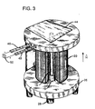
- a detailed illustration of an exemplary electromagnet 16, including bobbin 26, is shown in FIG. 3.
- bobbin 26 may also be formed to include the necessary electical connections between coil 20 and the external power supply.
- Bobbin 26 may be formed of any suitable material, including silicon, plastic or ceramic.
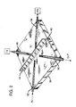
- FIG. 2 An exemplary switch substrate 13 which may utilize the activation mechanism of the present invention is illustrated in FIG. 2.
- the switch is utilized to connect a local user (referred to as a node) to a communication network.
- a local user referred to as a node
- the activation mechanism of the present invention is not considered to be dependent upon the particular use of the fiber switch.
- the activation mechanism of the present invention may also be used with a multiple switch array, where large numbers of optical signals may be switched simultaneously during a single operation of the activation means.
- a silicon substrate 30 is formed to hold a set of four fibers, including a fiber 32 which delivers the incoming optical signal through switch 10 to the node, a fiber 36 which delivers the outgoing signal from the node to the network, a fiber 34 coupled to the receiver portion of the node, and a fiber 38 which is coupled to the transmit portion of the node.
- the following discussion will describe the two positions (redirecting and attracted) of the exemplary switch.
- the redirecting position will be defined as the bypass state (where the node is removed from the network) and the attracted position will be defined as the active state (where the node is in communication with the network).
- the reflecting element is positioned as controlled by the activation mechanism such that the incoming optical signal will be intercepted and redirected into the outgoing fiber.
- the signal is thus redirected from incoming fiber 32 into outgoing fiber 36 by inserting a reflecting element 14 (e.g., mirror), as shown in phantom, in slot 40 of substrate 30.
- a reflecting element 14 e.g., mirror
- Separate lensing elements may be used to maximize the coupled power of the signal.
- both sides of element 14 upon which an optical signal may impinge contain a reflective coating. Therefore, the signal exiting fiber 38 (from the node transmitting device) may also be redirected by reflecting element 14 into fiber 34 associated with the node receiving device.
- the loopback of the local signal may be used by the node to perform maintenance operations on its local communication system during bypass conditions.
- the configuration as described is defined as the "redirecting" or "bypass" state of the switch.
- this active state of the switch is achieved by energizing the activation mechanism so as to attract the reflecting element and remove it from the optical signal path.
- the incoming signal along fiber 32 will then be launched into fiber 34 which is coupled to the node's receiver.
- the node transmitter is then used to launch a message signal into transmit fiber 38 which, in the absence of element 14, will pass unobstructed into outgoing fiber 36.
- the signal from the node transmitter is then returned via fiber 36 to the network.
- FIG. 3 An exemplary electromagnet 16 portion of an activation mechanism formed in accordance with the present invention is illustrated in FIG. 3.
- outer housing 42 of FIG. 1 has been removed so that the internal portions of electromagnet 16 are clearly visible.
- electromagnet 16 is energized by an external power supply 50 so as to raise reflecting element 14 in the presence of a magnetic field.
- Electromagnet 16 compises ferromagnetic core 18, for example, an iron alloy core, which is inserted through an opening in bobbin 26.
- bobbin 26 may comprise any suitable material, plastic being considered as the most economical alternative.
- a number of pins 28 may also be formed as part of bobbin 26 and disposed as shown in FIG. 3.
- Pins 28 are utilized to hold electromagnet 16 in a fixed position relative to the switch substrate such that the air gap separating reflecting element 14 and electromagnet 16 is precisely determined.
- a return path 44 comprising a sheet of ferromagnetic material, is disposed as shown in FIG. 3 and formed to contact top face 17 and approach (but not contact) bottom face 19 of core 18. The combination of core 18, ferromagnetic material 22 and return path 44 thus forms a complete ferromagnetic loop.
- Coil 20 is wound, as illustrated in FIG. 3, around bobbin 26 so as to encircle core 18.
- the wire forming coil 20 is attached, as shown, to a pair of electrical leads 46,48 for connection to external power supply 50.
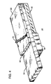
- FIG. 4 illustrates an exemplary reflecting element 14, which with electromagnet 16 of FIG. 3, forms an activation mechanism 12 as illustrated in FIG. 1.
- reflecting element 14 includes a mirror component 52 which performs the actual optical signal redirection.
- Mirror component 52 may comprise a section of mirrored glass or, alternatively, a section of silicon which has been processed to include suitable reflective coatings.
- Various other types of components may be used to form mirror 52.
- mirror component 52 is attached to (or formed as an integral part of) a support element 54 which is designed to maintain mirror component 52 in the required position in the optical signal path.
- support element 54 includes a pivot arm 56 which provides for movement of mirror component 52 in the illustrated direction upon activation of electromagnet 16.
- Support element 54 may further include, in association with the switch substrate, a number of registration markers 58 to facilitate alignment of reflecting element 14 with the switch substrate (not shown).
- a ferromagnetic material 22 is attached to top surface 60 of support element 54, as illustrated in FIG. 4, so as to be substantially underneath the position of electromagnet 16 relative to element 54.
- the thickness and extent of material 22 are sized according to many various design factors, including spring force, magnetic field intensity, switching time, etc.
- reflecting element 14 may further comprise a spring member 24, positioned as shown with respect to element 14 to aid in securing reflecting element 14 within the slot (redirecting position) of the switch substrate (illustrated in previous figures). End 62 of spring 24 is fixed within the housing (not shown) to provide the required rigidity. In operation, spring 24 is used to apply a relatively light force to top surface 60 of element 54, so as to maintain support element 54 properly aligned and reduce bounce, when electromagnet 16 is not activated.
- the activation mechanism of the present invention may be utilized to provide switching between a plurality of separate optical signals, such as in a 3x3 switch array as disclosed in the above-referenced copending application. Additionally, the activation mechanism of the present invention may be used to simultaneously move a number of separate reflecting elements, each element associated with a different switch.
- the switch itself is not necessarily limited to a fiber-based arrangement, where the activation mechanism of the present invention may also be used with a switch comprising a number of waveguides formed in an optical substrate, where the reflecting element of the inventive activation mechanism is disposed in a groove in the optical substrate.
- the switching mechanism itself is not considered to be limited to electromagnet-based embodiments, where there exist other means which are capable of providing the same motion of the reflecting element relative to the switch substrate.
Abstract
Description
- The present invention relates to an activation mechanism for an optical switch.
- In evolving optical communication networks, the need often arises to switch an optical signal from one path to another. For example, in a network which consists of a number of communication nodes connected sequentially to form a ring, it may be required to temporarily remove one or more nodes from the network. Therefore, the optical waveguides (e.g., fibers) interconnecting the network must be able to "switch" the node(s) from an active (transmit/receive) state to a passive (bypass) state. Many arrangements exist in the art for providing this type of switching. The arrangements may be generally classified into two groups: (1) moving beam switches (arrangements which redirect the optical signal path between stationary waveguides); and (2) moving fiber switches (designs which use an external force to physically change the location of optical fibers entering and exiting the node). The activation mechanism of the present invention is utilized with switches of the former design.
- An exemplary optical fiber switch utilizing a moving mirror to perform the switching function is disclosed in U.S. Patent 4,580,873, issued to F.H.Levinson on April 8, 1986. In the Levinson matrix switch, a plurality of mirrors are positioned at the crosspoints of the input and output nodes. As disclosed, a silicon switch substrate is etched to include regions at each crosspoint for holding a rotatable mirror assembly. The application of an electrical signal to individual mirror elements performs the switching function. Although such a switching arrangement may be practical for large array applications, the details of the silicon substrate fabrication process become increasingly time-consuming and expensive for single switch applications.
- A remaining need in these and other existing systems is the ability to reduce the overall size, cost, manufacturability and power consumption of the switch.
- The need remaining in the prior art is addressed by the present invention which relates to an activation mechanism for an optical switch and, more particularly, to means for moving a reflecting element into or out of an optical signal path between waveguides so as to provide switching of optical signals between pairs of waveguides.
- In general, the present invention relates to an activation mechanism comprising a reflecting element which, in a first position, redirects optical signals between pairs of optical waveguides. In a second position, the reflecting element is removed from the signal path so that the optical signals may pass through the switch unobstructed. The activation mechanism includes moving means located in close proximity to the reflecting element for providing a force (e.g., electrostatic, magnetic, vacuum) capable of moving the reflecting element towards the moving means and out of the optical signal path. For optical bypass switch applications, as will be discussed in detail below, the "first position" of the reflecting elements is usually used as the bypass state of the switch, and the "second position" is used as the active state of the switch.
- In accordance with a particular embodiment of the present invention, an electromagnetic device is utilized as the moving means and is positioned in close proximity to the reflecting element. A portion of the surface of the reflecting element near the electromagnetic device is coated with a ferromagnetic material (with a high magnetic permeability) to effect the attraction of the reflecting element to the electromagnetic moving means. In the absence of an applied electrical signal, the electromagnetic device is dormant and the reflecting element is positioned so as to intercept and redirect optical signals (first, redirecting position). Upon the application of an electrical signal to the electromagnet, a magnetic field is created which is of a sufficient strength to attract the ferromagnetic material on the reflecting element and move the element out of the optical signal path (second, attracted position) so as to allow the optical signals to pass through the switch unobstructed by the reflecting element.
- As an additional feature of the present invention, a spring member may be positioned on the reflecting element to aid in securing the reflecting element in the redirecting position. The spring element is of a force which does not interfere with the operation of the moving means, yet may speed the return of the reflecting element to its redirecting position when the external signal is removed and the moving means is deactivated.
- An advantage of the activation mechanism of the present invention is that the mechanism is totally encased and may be located above (or below) the set of optical waveguides such that no additional surface area beyond the substrate holding the waveguides is required.
- Another advantage of the activation mechanism of the present invention is that the gap separating the reflecting element and the moving means may be made extremely small (e.g., on the order of 10 mils), so that the force (and hence, the external electric power) required to lift the reflecting element is reduced. The reduction in air gap size also serves to decrease the overall size of the switch. Further, a particular embodiment of the present invention utilizes housing for the moving means including a number of support pins. The support pins are positioned so as to inherently provide for a well-defined, reproducible and tightly toleranced air gap separating the two members.
- Various other embodiment, features and advantages of the present invention will become apparent during the following discussion and by reference to the accompanying drawings.
- Referring now to the drawings, where like numerals represent like parts in several views:
- FIG. 1 illustrates a cut away view of an exemplary optical switch utilizing an exemplary electromagnet-based activation mechanism of the present invention;
- FIG. 2 illustrates in detail the substrate portion of an exemplary optical fiber switch which may utilize the activation mechanism of the present invention;
- FIG. 3 contains a detailed illustration of an exemplary activation mechanism formed in accordance with the present invention; and
- FIG. 4 contains a detailed illustration of an exemplary reflecting element formed in accordance with the present invention.
- In the general operation of the present invention, the reflecting element is positioned in the optical signal path (first, redirecting position) so as to redirect signals between appropriate input and output optical waveguides. Upon the application of an external force, the reflecting element is removed from the signal path (second, attracted position) so that the optical waves propagate unobstructed.
- The external force may be electrostatic, vacuum, magnetic, or any other type of force suitable for providing motion of the reflecting element in response to an applied signal.
- An exemplary
optical fiber switch 10 including an exemplary electromagnetic-based activation mechanism 12 of the present invention is illustrated in FIG. 1. The portion of the switch holding the actual fibers, referred to as aswitch substrate 13, is illustrated more clearly in FIG. 2 and will be described in detail below. It is to be understood that the use of the activation mechanism of the present invention is not limited to fiber-based optical switches, but is generally applicable to switch optical signals traveling along any type of optical waveguide. As used herein, the term "optical waveguide" is deemed to encompass not only integrated waveguides formed within an optical substrate, but also optical fibers, or in general any media capable of supporting the transport of an optical signal. Additionally, an exemplary switch utilizing the activation mechanism of the present invention may use any desired combination of optical fibers and integrated waveguides. it is to be noted that the following discussion describes a particular embodiment of the present invention which utilizes a magnetically-controlled activation mechanism. As discussed above, other types of control arrangements (e.g., electrostatic, vacuum) may also be used. - Returning to FIG. 1,
switch 10 includes anactivation mechanism 12 which functions to move a reflectingelement 14 out of its redirecting position upon application of an electrical signal. In particular,activation mechanism 12 includes an electromagnet 16 comprising aferromagnetic core 18 and awire coil 20 which is wound aroundcore 18. As is well known in the art, the application of an electrical signal (i.e., voltage) tocoil 20 will create a magnetic field intensity, denoted Ĥ, in the direction illustrated in FIG. 1. - At least a portion surface of reflecting
element 14 located in proximity tocore 18 is coated with aferromagnetic material 22 which will be attracted tocore 18 in the presence of the induced field Ĥ. As will be discussed below in association with FIG. 2, the magnetic field functions to attract reflectingelement 14, movingelement 14 out of the optical signal path. The attracted position ofswitch 10 is illustrated in FIG. 1, where communication is unobstructed between anincoming fiber 32 and anoutgoing fiber 34. As can be seen by reference to FIG. 1, only the slightest raising is required to effectively remove reflectingelement 14 from the signal path. - A
spring member 24, illustrated in FIG. 1 (shown more clearly in FIG. 4), may be used to maintain reflectingelement 14 in the redirecting position and thus prevent "bouncing" ofelement 14 in the absence of magnetic field intensity Ĥ (i.e., applied voltage). As mentioned above, the spring force is such that reflectingelement 14 remains motionless in the redirecting position, yet is insufficient to interfere with the operation of electromagnet 16. - In an alternative vacuum-controlled embodiment of the activation mechanism of the present invention,
ferromagnetic core 18 described above may be replaced by a hollow tube, connected to a vacuum source. Therefore, upon the activation of the vacuum source, the force of the vacuum will attract the reflecting element towards the hollow tube. - In
packaging activation mechanism 12 withswitch 10, the embodiment of FIG. 1 illustratescoil 20 being wound on abobbin 26, withferromagnetic core 18 being positioned in a central opening throughbobbin 26. As shown,bobbin 26 includes a set ofpins 28 which serve to supportbobbin 26 in a fixed and stable position aboveswitch substrate 13. As mentioned above, the dimensions (height) of the pins will also serve to determine the air gap separatingferromagnetic core 18 andferromagnetic material 22. Advantageously, the air gap will then be a well-controlled and reproducible quantity. A detailed illustration of an exemplary electromagnet 16, includingbobbin 26, is shown in FIG. 3. As will be discussed in detail hereinafter,bobbin 26 may also be formed to include the necessary electical connections betweencoil 20 and the external power supply.Bobbin 26 may be formed of any suitable material, including silicon, plastic or ceramic. - An
exemplary switch substrate 13 which may utilize the activation mechanism of the present invention is illustrated in FIG. 2. In this particular application, the switch is utilized to connect a local user (referred to as a node) to a communication network. It is to be noted that there exist other uses for such a switch, such as in a laser sparing operation where it is desired to disconnect afirst signal source and connect a second signal source to an outgoing communication fiber. The activation mechanism of the present invention is not considered to be dependent upon the particular use of the fiber switch. For example, the activation mechanism of the present invention may also be used with a multiple switch array, where large numbers of optical signals may be switched simultaneously during a single operation of the activation means. Various ones of these different switching embodiments are described in detail in a copending application entitled "Radiation Switching Arrangement with Moving Deflective Element", Serial No. 385,331, filed July 25, 1989, assigned to the assignee of this invention and herein incorporated by reference. - In the particular embodiment illustrated in FIG. 2, a
silicon substrate 30 is formed to hold a set of four fibers, including afiber 32 which delivers the incoming optical signal throughswitch 10 to the node, afiber 36 which delivers the outgoing signal from the node to the network, afiber 34 coupled to the receiver portion of the node, and afiber 38 which is coupled to the transmit portion of the node. The following discussion will describe the two positions (redirecting and attracted) of the exemplary switch. For the particular discussion, the redirecting position will be defined as the bypass state (where the node is removed from the network) and the attracted position will be defined as the active state (where the node is in communication with the network). With respect to the bypass state, the reflecting element is positioned as controlled by the activation mechanism such that the incoming optical signal will be intercepted and redirected into the outgoing fiber. Referring to FIG. 2, the signal is thus redirected fromincoming fiber 32 intooutgoing fiber 36 by inserting a reflecting element 14 (e.g., mirror), as shown in phantom, inslot 40 ofsubstrate 30. Separate lensing elements may be used to maximize the coupled power of the signal. In general, both sides ofelement 14 upon which an optical signal may impinge contain a reflective coating. Therefore, the signal exiting fiber 38 (from the node transmitting device) may also be redirected by reflectingelement 14 intofiber 34 associated with the node receiving device. Advantageously, the loopback of the local signal may be used by the node to perform maintenance operations on its local communication system during bypass conditions. The configuration as described is defined as the "redirecting" or "bypass" state of the switch. In accordance with the teachings of the present invention, it is preferred to utilize the unenergized state of the activation mechanism to define the bypass state, since a power failure at the node would thus automatically disconnect from the network. - In most cases, it is desired to have the node in communication with the network. In accordance with the teachings of the present invention, this active state of the switch is achieved by energizing the activation mechanism so as to attract the reflecting element and remove it from the optical signal path. Referring to FIG. 2, if
element 14 is removed from the signal path, the incoming signal alongfiber 32 will then be launched intofiber 34 which is coupled to the node's receiver. The node transmitter is then used to launch a message signal into transmitfiber 38 which, in the absence ofelement 14, will pass unobstructed intooutgoing fiber 36. The signal from the node transmitter is then returned viafiber 36 to the network. As mentioned above, a detailed description of the operation of this particular switch may be had by reviewing the above-referenced application. With this explanation of the operation ofswitch 10, various components visible in FIG. 1 may now be identified, includingincoming fiber 32,receiver fiber 34 andgroove 40. - An exemplary electromagnet 16 portion of an activation mechanism formed in accordance with the present invention is illustrated in FIG. 3. For the sake of clarity,
outer housing 42 of FIG. 1 has been removed so that the internal portions of electromagnet 16 are clearly visible. As discussed above, electromagnet 16 is energized by anexternal power supply 50 so as to raise reflectingelement 14 in the presence of a magnetic field. Electromagnet 16 compisesferromagnetic core 18, for example, an iron alloy core, which is inserted through an opening inbobbin 26. As mentioned above,bobbin 26 may comprise any suitable material, plastic being considered as the most economical alternative. A number ofpins 28 may also be formed as part ofbobbin 26 and disposed as shown in FIG. 3.Pins 28 are utilized to hold electromagnet 16 in a fixed position relative to the switch substrate such that the air gap separating reflectingelement 14 and electromagnet 16 is precisely determined. Areturn path 44, comprising a sheet of ferromagnetic material, is disposed as shown in FIG. 3 and formed to contacttop face 17 and approach (but not contact)bottom face 19 ofcore 18. The combination ofcore 18,ferromagnetic material 22 and returnpath 44 thus forms a complete ferromagnetic loop.Coil 20 is wound, as illustrated in FIG. 3, aroundbobbin 26 so as to encirclecore 18. Thewire forming coil 20 is attached, as shown, to a pair ofelectrical leads external power supply 50. - In operation, when
power supply 50 is turned on, the voltage V applied betweenleads coil 20. As is well-known, the flow of a current in a coil wound around a ferromagnetic material will result in the creation of a magnetic field, illustrated as Ĥ. The strength of the magnetic field is thus a function of the level of the current, the number of turns ofcoil 20, and the selected materials. - FIG. 4 illustrates an exemplary reflecting
element 14, which with electromagnet 16 of FIG. 3, forms anactivation mechanism 12 as illustrated in FIG. 1. Referring to FIG. 4, reflectingelement 14 includes amirror component 52 which performs the actual optical signal redirection.Mirror component 52 may comprise a section of mirrored glass or, alternatively, a section of silicon which has been processed to include suitable reflective coatings. Various other types of components may be used to formmirror 52. As shown,mirror component 52 is attached to (or formed as an integral part of) asupport element 54 which is designed to maintainmirror component 52 in the required position in the optical signal path. For the particular embodiment illustrated in FIG. 4,support element 54 includes apivot arm 56 which provides for movement ofmirror component 52 in the illustrated direction upon activation of electromagnet 16.Support element 54 may further include, in association with the switch substrate, a number of registration markers 58 to facilitate alignment of reflectingelement 14 with the switch substrate (not shown). Aferromagnetic material 22 is attached totop surface 60 ofsupport element 54, as illustrated in FIG. 4, so as to be substantially underneath the position of electromagnet 16 relative toelement 54. The thickness and extent ofmaterial 22 are sized according to many various design factors, including spring force, magnetic field intensity, switching time, etc. - As mentioned above, reflecting
element 14 may further comprise aspring member 24, positioned as shown with respect toelement 14 to aid in securing reflectingelement 14 within the slot (redirecting position) of the switch substrate (illustrated in previous figures). End 62 ofspring 24 is fixed within the housing (not shown) to provide the required rigidity. In operation,spring 24 is used to apply a relatively light force totop surface 60 ofelement 54, so as to maintainsupport element 54 properly aligned and reduce bounce, when electromagnet 16 is not activated. - It is to be understood that the above-described embodiments are merely illustrative of the teachings of the present invention and should not be considered to limit the scope of the inventive activation mechanism. For example, the activation mechanism of the present invention may be utilized to provide switching between a plurality of separate optical signals, such as in a 3x3 switch array as disclosed in the above-referenced copending application. Additionally, the activation mechanism of the present invention may be used to simultaneously move a number of separate reflecting elements, each element associated with a different switch. Further, the switch itself is not necessarily limited to a fiber-based arrangement, where the activation mechanism of the present invention may also be used with a switch comprising a number of waveguides formed in an optical substrate, where the reflecting element of the inventive activation mechanism is disposed in a groove in the optical substrate. Lastly, as mentioned above, the switching mechanism itself is not considered to be limited to electromagnet-based embodiments, where there exist other means which are capable of providing the same motion of the reflecting element relative to the switch substrate.
Claims (10)
- In an optical switch utilizing a reflecting element to redirect optical signals between a number of different communication paths, an activation mechanism for providing the redirection of optical signals,
CHARACTERIZED IN THAT
the activation mechanism (e.g., 12) comprises
a reflecting element (e.g., 14) for directing signals when disposed in a first position and for passing signals when in a second position; and
moving means (e.g., 16) disposed in close proximity to the reflecting element and separated therefrom by a distance sufficient to allow the reflecting element to be moved out of the optical signal path upon activation of the moving means. - An optical switch as defined in claim 1 wherein the activation mechanism moving means comprises electromagnetic means (e.g., 18, 20) capable of attracting the reflecting element for providing the second position of said switch, said reflecting element further comprising a coating of ferromagnetic material (e.g., 22) disposed in proximity to the electromagnetic device.
- An optical switch as defined in claim 2 wherein the activation mechanism electromagnetic means comprises
a bobbin (e.g., 26) including a hollow core region;
a wire coil (e.g., 20) wound around the bobbin, the coil including a sufficient number of turns to provide the desired magnetic field;
a ferromagnetic core (e.g., 18) disposed within the hollow core region of the bobbin, the core defined as having first and second endfaces formed to be relatively flush with the bobbin;
a ferromagnetic return path (e.g., 44) surrounding a portion of the bobbin so as to contact the first endface of the core; and
electrical connection means (e.g., 46, 48) coupled to the first and second ends of the wire coil for connecting the wire coil to an external power supply. - An optical switch as defined in claim 3 wherein the bobbin further includes a plurality of pins (e.g., 28) for supporting the electromagnetic means a predetermined distance above the reflecting element, or comprises plastic material.
- An optical switch as defined in claim 3, wherein the ferromagnetic core and ferromagnetic return path comprise an iron alloy.
- An optical switch as defined in claim 2 wherein the activation mechanism reflecting element comprises:
a mirror (e.g., 52) for providing the optical signal redirection path; and
a mirror support element (e.g., 54) for holding the mirror in the optical signal redirection path; and
a ferromagnetic coating (e.g., 22) disposed on said reflecting element so as to be located underneath the electromagnet. - An optical switch as defined in claim 1 or 6 wherein the activation mechanism reflecting element further comprises a pivot arm (e.g., 56) for controlling the motion of said reflecting element; or
further comprises a plurality of registration markers (e.g., 58) for facilitating alignment of said reflecting element with the communication paths; or
further comprises a spring member (e.g., 24) capable of maintaining the mirror in a fixed location in the optical signal redirecting position, the spring force being insufficient to negate the attraction of the electromagnetic means; or
comprises a single reflecting component; or
a plurality of reflecting components simultaneously activated by the moving means. - An optical switch as defined in claim 1 wherein the activation mechanism further comprises a plurality of pins for supporting the moving means a predetermined distance above the reflecting element.
- An optical switch as defined in claim 1 wherein the activation mechanism reflecting element further comprises
a mirror for providing the optical signal redirection path;
and
a mirror support element for holding the mirror in the optical signal redirection path. - An optical switch as defined in claim 6, wherein the mirror support element comprises silicon.
Applications Claiming Priority (2)
| Application Number | Priority Date | Filing Date | Title |
|---|---|---|---|
| US07/506,310 US5042889A (en) | 1990-04-09 | 1990-04-09 | Magnetic activation mechanism for an optical switch |
| US506310 | 1990-04-09 |
Publications (2)
| Publication Number | Publication Date |
|---|---|
| EP0452012A2 true EP0452012A2 (en) | 1991-10-16 |
| EP0452012A3 EP0452012A3 (en) | 1991-12-18 |
Family
ID=24014067
Family Applications (1)
| Application Number | Title | Priority Date | Filing Date |
|---|---|---|---|
| EP19910302817 Withdrawn EP0452012A3 (en) | 1990-04-09 | 1991-03-28 | Activation mechanism for an optical switch |
Country Status (3)
| Country | Link |
|---|---|
| US (1) | US5042889A (en) |
| EP (1) | EP0452012A3 (en) |
| JP (1) | JPH04225311A (en) |
Cited By (16)
| Publication number | Priority date | Publication date | Assignee | Title |
|---|---|---|---|---|
| WO2002005012A2 (en) * | 2000-07-11 | 2002-01-17 | Arizona State University | Optical mems switching array with embedded beam-confining channels and method of operating same |
| EP1189092A2 (en) * | 2000-09-06 | 2002-03-20 | Japan Aviation Electronics Industry, Limited | Electrostatically operated optical switch |
| US6836194B2 (en) | 2001-12-21 | 2004-12-28 | Magfusion, Inc. | Components implemented using latching micro-magnetic switches |
| US6894592B2 (en) | 2001-05-18 | 2005-05-17 | Magfusion, Inc. | Micromagnetic latching switch packaging |
| US7027682B2 (en) | 1999-09-23 | 2006-04-11 | Arizona State University | Optical MEMS switching array with embedded beam-confining channels and method of operating same |
| US7183884B2 (en) | 2003-10-15 | 2007-02-27 | Schneider Electric Industries Sas | Micro magnetic non-latching switches and methods of making same |
| US7202765B2 (en) | 2003-05-14 | 2007-04-10 | Schneider Electric Industries Sas | Latchable, magnetically actuated, ground plane-isolated radio frequency microswitch |
| US7215229B2 (en) | 2003-09-17 | 2007-05-08 | Schneider Electric Industries Sas | Laminated relays with multiple flexible contacts |
| US7250838B2 (en) | 2002-01-08 | 2007-07-31 | Schneider Electric Industries Sas | Packaging of a micro-magnetic switch with a patterned permanent magnet |
| US7253710B2 (en) | 2001-12-21 | 2007-08-07 | Schneider Electric Industries Sas | Latching micro-magnetic switch array |
| US7266867B2 (en) | 2002-09-18 | 2007-09-11 | Schneider Electric Industries Sas | Method for laminating electro-mechanical structures |
| US7300815B2 (en) | 2002-09-30 | 2007-11-27 | Schneider Electric Industries Sas | Method for fabricating a gold contact on a microswitch |
| US7327211B2 (en) | 2002-01-18 | 2008-02-05 | Schneider Electric Industries Sas | Micro-magnetic latching switches with a three-dimensional solenoid coil |
| US7342473B2 (en) | 2004-04-07 | 2008-03-11 | Schneider Electric Industries Sas | Method and apparatus for reducing cantilever stress in magnetically actuated relays |
| US7391290B2 (en) | 2003-10-15 | 2008-06-24 | Schneider Electric Industries Sas | Micro magnetic latching switches and methods of making same |
| US7420447B2 (en) | 2002-03-18 | 2008-09-02 | Schneider Electric Industries Sas | Latching micro-magnetic switch with improved thermal reliability |
Families Citing this family (31)
| Publication number | Priority date | Publication date | Assignee | Title |
|---|---|---|---|---|
| US5226099A (en) * | 1991-04-26 | 1993-07-06 | Texas Instruments Incorporated | Digital micromirror shutter device |
| US5436986A (en) * | 1993-03-09 | 1995-07-25 | Tsai; Jian-Hung | Apparatus for switching optical signals among optical fibers and method |
| US5642446A (en) * | 1993-03-09 | 1997-06-24 | Tsai; Jian-Hung | Apparatus for switching optical signals among optical fibers |
| FR2714886B1 (en) * | 1994-01-10 | 1996-03-29 | Labinal | Light signaling device on aircraft. |
| US5841917A (en) * | 1997-01-31 | 1998-11-24 | Hewlett-Packard Company | Optical cross-connect switch using a pin grid actuator |
| US6498870B1 (en) | 1998-04-20 | 2002-12-24 | Omm, Inc. | Micromachined optomechanical switches |
| US6269201B1 (en) | 1998-08-07 | 2001-07-31 | Lightech Fiberoptics Inc. | Multi-channel fiber optical switch |
| US6870595B1 (en) * | 1998-09-22 | 2005-03-22 | Minolta Co., Ltd. | Optical filter device and method of making same |
| US6256430B1 (en) * | 1998-11-23 | 2001-07-03 | Agere Systems Inc. | Optical crossconnect system comprising reconfigurable light-reflecting devices |
| US6154586A (en) * | 1998-12-24 | 2000-11-28 | Jds Fitel Inc. | Optical switch mechanism |
| US6215222B1 (en) | 1999-03-30 | 2001-04-10 | Agilent Technologies, Inc. | Optical cross-connect switch using electrostatic surface actuators |
| US6445840B1 (en) | 1999-05-28 | 2002-09-03 | Omm, Inc. | Micromachined optical switching devices |
| US6445841B1 (en) | 1999-05-28 | 2002-09-03 | Omm, Inc. | Optomechanical matrix switches including collimator arrays |
| US6449406B1 (en) | 1999-05-28 | 2002-09-10 | Omm, Inc. | Micromachined optomechanical switching devices |
| US6453083B1 (en) | 1999-05-28 | 2002-09-17 | Anis Husain | Micromachined optomechanical switching cell with parallel plate actuator and on-chip power monitoring |
| US6407838B1 (en) | 1999-07-21 | 2002-06-18 | Luxn, Inc. | Reconfigurable multi-add/drop module for optical communications |
| US6351580B1 (en) | 2000-03-27 | 2002-02-26 | Jds Uniphase Corporation | Microelectromechanical devices having brake assemblies therein to control movement of optical shutters and other movable elements |
| US6751369B1 (en) | 2000-07-28 | 2004-06-15 | Moog Components Group Inc. | Fiber lens assembly for singlemode optical switches |
| US6388789B1 (en) | 2000-09-19 | 2002-05-14 | The Charles Stark Draper Laboratory, Inc. | Multi-axis magnetically actuated device |
| US6591027B2 (en) | 2001-02-27 | 2003-07-08 | Litton Systems, Inc. | Bi-stable micro-actuator and optical switch |
| US6788840B2 (en) | 2001-02-27 | 2004-09-07 | Northrop Grumman Corporation | Bi-stable micro-actuator and optical switch |
| US6665461B1 (en) | 2001-04-05 | 2003-12-16 | Richard H. Laughlin | Total internal reflection optical switch and method of operating the same |
| US6859578B2 (en) * | 2001-05-18 | 2005-02-22 | Nuonics, Inc. | Fault-tolerant fiber-optical multiwavelength processor |
| US20030103262A1 (en) * | 2001-09-07 | 2003-06-05 | Board Of Regents, The University Of Texas System | Multimodal miniature microscope |
| TW495039U (en) * | 2001-10-31 | 2002-07-11 | Hon Hai Prec Ind Co Ltd | Reflection plane movable light switch |
| US6831772B2 (en) | 2002-02-01 | 2004-12-14 | Analog Devices, Inc. | Optical mirror module |
| US6798942B2 (en) * | 2002-04-05 | 2004-09-28 | Finisar Corporation | Zero static power optical switch |
| EP1512037A1 (en) * | 2002-06-12 | 2005-03-09 | Microcut AG | Electromagnetic linear optical positioner |
| US6823102B2 (en) * | 2002-07-22 | 2004-11-23 | Agiltron, Inc. | Highly stable opto-mechanic switches |
| JP3952902B2 (en) * | 2002-08-09 | 2007-08-01 | 住友電気工業株式会社 | Optical switch, optical add / drop device, optical transmission system, and optical switch manufacturing method |
| WO2010080158A1 (en) * | 2009-01-09 | 2010-07-15 | Hewlett-Packard Development Company, L.P. | Configurable point-to-point optical communications system between servers |
Citations (5)
| Publication number | Priority date | Publication date | Assignee | Title |
|---|---|---|---|---|
| US4580873A (en) * | 1983-12-30 | 1986-04-08 | At&T Bell Laboratories | Optical matrix switch |
| WO1987002518A1 (en) * | 1985-10-16 | 1987-04-23 | British Telecommunications Public Limited Company | Mounting a component to a substrate |
| EP0221288A1 (en) * | 1985-10-04 | 1987-05-13 | Socapex S.A. | Electromagnetically operated optical switch |
| DE3608134A1 (en) * | 1986-03-12 | 1987-09-24 | Ant Nachrichtentech | Optical switch |
| JPS63131118A (en) * | 1986-11-21 | 1988-06-03 | Nippon Telegr & Teleph Corp <Ntt> | Optical path switching device |
Family Cites Families (10)
| Publication number | Priority date | Publication date | Assignee | Title |
|---|---|---|---|---|
| US4057719A (en) * | 1976-08-27 | 1977-11-08 | The United States Of America As Represented By The Secretary Of The Navy | Fiber optics electro-mechanical light switch |
| JPS54161952A (en) * | 1978-06-13 | 1979-12-22 | Nippon Telegr & Teleph Corp <Ntt> | Photo switch |
| JPS5574503A (en) * | 1978-11-29 | 1980-06-05 | Nec Corp | Mechanical photo switch |
| JPS55130505A (en) * | 1979-03-30 | 1980-10-09 | Ryohei Itaya | Photoswitch |
| US4376566A (en) * | 1980-03-03 | 1983-03-15 | Sheltered Workshop For The Disabled, Inc. | Fiber optic switching method and apparatus with flexible shutter |
| US4512627A (en) * | 1982-12-13 | 1985-04-23 | At&T Bell Laboratories | Optical fiber switch, electromagnetic actuating apparatus with permanent magnet latch control |
| US4607161A (en) * | 1983-10-11 | 1986-08-19 | Fiberdynamics, Inc. | Fiberoptic switch system |
| JPS6385521A (en) * | 1986-09-29 | 1988-04-16 | Omron Tateisi Electronics Co | Optical switch |
| US4790621A (en) * | 1987-12-07 | 1988-12-13 | Gte Products Corporation | Fiber optic switch |
| US4932745A (en) * | 1989-07-25 | 1990-06-12 | At&T Bell Laboratories | Radiation switching arrangement with moving deflecting element |
-
1990
- 1990-04-09 US US07/506,310 patent/US5042889A/en not_active Expired - Lifetime
-
1991
- 1991-03-28 EP EP19910302817 patent/EP0452012A3/en not_active Withdrawn
- 1991-04-01 JP JP3092610A patent/JPH04225311A/en active Pending
Patent Citations (5)
| Publication number | Priority date | Publication date | Assignee | Title |
|---|---|---|---|---|
| US4580873A (en) * | 1983-12-30 | 1986-04-08 | At&T Bell Laboratories | Optical matrix switch |
| EP0221288A1 (en) * | 1985-10-04 | 1987-05-13 | Socapex S.A. | Electromagnetically operated optical switch |
| WO1987002518A1 (en) * | 1985-10-16 | 1987-04-23 | British Telecommunications Public Limited Company | Mounting a component to a substrate |
| DE3608134A1 (en) * | 1986-03-12 | 1987-09-24 | Ant Nachrichtentech | Optical switch |
| JPS63131118A (en) * | 1986-11-21 | 1988-06-03 | Nippon Telegr & Teleph Corp <Ntt> | Optical path switching device |
Non-Patent Citations (2)
| Title |
|---|
| IBM TECHNICAL DISCLOSURE BULLETIN, vol. 27, no. 2, July 1984, NEW YORK, US; pages 1119 - 1120; M.B.Callaway et al.: "ARRAY LIGHT VALVE SWITCHES INFORMATION SIGNALS BETWEEN FIBER-OPTIC SIGNAL CONDUCTORS" * |
| PATENT ABSTRACTS OF JAPAN, vol. 12, no. 388 (P-771)[3235] 17 October 1988; & JP-A-63 131 118 (NIPPON TELEGR & TELEPH) 3 June 1988, * |
Cited By (20)
| Publication number | Priority date | Publication date | Assignee | Title |
|---|---|---|---|---|
| US7027682B2 (en) | 1999-09-23 | 2006-04-11 | Arizona State University | Optical MEMS switching array with embedded beam-confining channels and method of operating same |
| WO2002005012A3 (en) * | 2000-07-11 | 2002-06-27 | Univ Arizona | Optical mems switching array with embedded beam-confining channels and method of operating same |
| WO2002005012A2 (en) * | 2000-07-11 | 2002-01-17 | Arizona State University | Optical mems switching array with embedded beam-confining channels and method of operating same |
| EP1189092A2 (en) * | 2000-09-06 | 2002-03-20 | Japan Aviation Electronics Industry, Limited | Electrostatically operated optical switch |
| EP1189092A3 (en) * | 2000-09-06 | 2003-01-02 | Japan Aviation Electronics Industry, Limited | Electrostatically operated optical switch |
| US6625343B2 (en) | 2000-09-06 | 2003-09-23 | Japan Aviation Electronics Industry Limited | Optical switch |
| US6894592B2 (en) | 2001-05-18 | 2005-05-17 | Magfusion, Inc. | Micromagnetic latching switch packaging |
| US7372349B2 (en) | 2001-05-18 | 2008-05-13 | Schneider Electric Industries Sas | Apparatus utilizing latching micromagnetic switches |
| US6836194B2 (en) | 2001-12-21 | 2004-12-28 | Magfusion, Inc. | Components implemented using latching micro-magnetic switches |
| US7253710B2 (en) | 2001-12-21 | 2007-08-07 | Schneider Electric Industries Sas | Latching micro-magnetic switch array |
| US7250838B2 (en) | 2002-01-08 | 2007-07-31 | Schneider Electric Industries Sas | Packaging of a micro-magnetic switch with a patterned permanent magnet |
| US7327211B2 (en) | 2002-01-18 | 2008-02-05 | Schneider Electric Industries Sas | Micro-magnetic latching switches with a three-dimensional solenoid coil |
| US7420447B2 (en) | 2002-03-18 | 2008-09-02 | Schneider Electric Industries Sas | Latching micro-magnetic switch with improved thermal reliability |
| US7266867B2 (en) | 2002-09-18 | 2007-09-11 | Schneider Electric Industries Sas | Method for laminating electro-mechanical structures |
| US7300815B2 (en) | 2002-09-30 | 2007-11-27 | Schneider Electric Industries Sas | Method for fabricating a gold contact on a microswitch |
| US7202765B2 (en) | 2003-05-14 | 2007-04-10 | Schneider Electric Industries Sas | Latchable, magnetically actuated, ground plane-isolated radio frequency microswitch |
| US7215229B2 (en) | 2003-09-17 | 2007-05-08 | Schneider Electric Industries Sas | Laminated relays with multiple flexible contacts |
| US7183884B2 (en) | 2003-10-15 | 2007-02-27 | Schneider Electric Industries Sas | Micro magnetic non-latching switches and methods of making same |
| US7391290B2 (en) | 2003-10-15 | 2008-06-24 | Schneider Electric Industries Sas | Micro magnetic latching switches and methods of making same |
| US7342473B2 (en) | 2004-04-07 | 2008-03-11 | Schneider Electric Industries Sas | Method and apparatus for reducing cantilever stress in magnetically actuated relays |
Also Published As
| Publication number | Publication date |
|---|---|
| EP0452012A3 (en) | 1991-12-18 |
| US5042889A (en) | 1991-08-27 |
| JPH04225311A (en) | 1992-08-14 |
Similar Documents
| Publication | Publication Date | Title |
|---|---|---|
| US5042889A (en) | Magnetic activation mechanism for an optical switch | |
| US4322126A (en) | Mechanical optical switching devices | |
| US6256430B1 (en) | Optical crossconnect system comprising reconfigurable light-reflecting devices | |
| US6259835B1 (en) | Mechanically actuated optical switch | |
| US4303303A (en) | Mechanical optical switching device | |
| US7095917B2 (en) | Optical switching apparatus | |
| JP3115779B2 (en) | Switchable optical fiber connector device | |
| US4582391A (en) | Optical switch, and a matrix of such switches | |
| US7027682B2 (en) | Optical MEMS switching array with embedded beam-confining channels and method of operating same | |
| TW457381B (en) | Fiber optic switching apparatus and method | |
| JP2000098270A5 (en) | ||
| US6404969B1 (en) | Optical switching and attenuation systems and methods therefor | |
| US6208777B1 (en) | Actuator assembly for optical switches | |
| US6424759B1 (en) | Mechanically actuated MXN optical switch matrix | |
| EP0526534B1 (en) | High speed shutter mechanism for a light beam | |
| US6738538B2 (en) | Method to construct optical infrastructure on a wafer | |
| US6975788B2 (en) | Optical switch having combined input/output fiber array | |
| KR20030050798A (en) | Magnetic Drive Micromirror and Method for Fabricating the same, and Optical Switch using the same | |
| US6798942B2 (en) | Zero static power optical switch | |
| JP2004145348A (en) | Optical switch | |
| US20040013349A1 (en) | Method and apparatus for optical switching with same side input and outputs | |
| US6898344B2 (en) | Fiber optic switch actuator | |
| JP2002323663A (en) | Cross-connect optical switch | |
| WO1992020002A1 (en) | Ruggedized bypass switch | |
| JP2001264652A (en) | Optical switch |
Legal Events
| Date | Code | Title | Description |
|---|---|---|---|
| PUAI | Public reference made under article 153(3) epc to a published international application that has entered the european phase |
Free format text: ORIGINAL CODE: 0009012 |
|
| AK | Designated contracting states |
Kind code of ref document: A2 Designated state(s): DE FR GB |
|
| PUAL | Search report despatched |
Free format text: ORIGINAL CODE: 0009013 |
|
| AK | Designated contracting states |
Kind code of ref document: A3 Designated state(s): DE FR GB |
|
| 17P | Request for examination filed |
Effective date: 19920610 |
|
| 17Q | First examination report despatched |
Effective date: 19940117 |
|
| RAP3 | Party data changed (applicant data changed or rights of an application transferred) |
Owner name: AT&T CORP. |
|
| STAA | Information on the status of an ep patent application or granted ep patent |
Free format text: STATUS: THE APPLICATION IS DEEMED TO BE WITHDRAWN |
|
| 18D | Application deemed to be withdrawn |
Effective date: 19940528 |