EP0446019A2 - Image processing apparatus and method - Google Patents
Image processing apparatus and method Download PDFInfo
- Publication number
- EP0446019A2 EP0446019A2 EP91301823A EP91301823A EP0446019A2 EP 0446019 A2 EP0446019 A2 EP 0446019A2 EP 91301823 A EP91301823 A EP 91301823A EP 91301823 A EP91301823 A EP 91301823A EP 0446019 A2 EP0446019 A2 EP 0446019A2
- Authority
- EP
- European Patent Office
- Prior art keywords
- image processing
- color correction
- color
- data
- image
- Prior art date
- Legal status (The legal status is an assumption and is not a legal conclusion. Google has not performed a legal analysis and makes no representation as to the accuracy of the status listed.)
- Granted
Links
Images


Classifications
-
- G—PHYSICS
- G06—COMPUTING; CALCULATING OR COUNTING
- G06T—IMAGE DATA PROCESSING OR GENERATION, IN GENERAL
- G06T1/00—General purpose image data processing
-
- H—ELECTRICITY
- H04—ELECTRIC COMMUNICATION TECHNIQUE
- H04N—PICTORIAL COMMUNICATION, e.g. TELEVISION
- H04N1/00—Scanning, transmission or reproduction of documents or the like, e.g. facsimile transmission; Details thereof
- H04N1/46—Colour picture communication systems
-
- H—ELECTRICITY
- H04—ELECTRIC COMMUNICATION TECHNIQUE
- H04N—PICTORIAL COMMUNICATION, e.g. TELEVISION
- H04N1/00—Scanning, transmission or reproduction of documents or the like, e.g. facsimile transmission; Details thereof
- H04N1/46—Colour picture communication systems
- H04N1/56—Processing of colour picture signals
- H04N1/60—Colour correction or control
- H04N1/62—Retouching, i.e. modification of isolated colours only or in isolated picture areas only
Definitions
- the present invention relates to an image processing apparatus and, more particularly to an image processing apparatus for processing image data with color information.
- a conventional color printing apparatus was so constructed that a predetermined color reproduction process is performed, and had not any other operation modes which simplify the color reproduction process for printing.
- a natural picture is mainly processed, and therefore even for an object image, in which characters and graphic forms prepared by a computer are mixed with the natural picture, a color correction process similar to the above-mentioned process is performed.
- the conventional example had a defect that the masking, black generation, under color removal, etc. are performed also for characters, which should be originally recorded all in black, and graphic forms, which should be painted out in a color specified by a color sample.
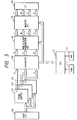
- Fig.1 is a block diagram showing the circuit configuration of a printing apparatus in the first embodiment according to the present invention.
- the printing apparatus according to this embodiment is composed of a host computer 1 and the printing apparatus body 2.
- the host computer 1 transmits print data (character data, graphic data, bit map data), print command (paper size, number of papers, etc.), etc. to the printing apparatus body 2 to allow this printing apparatus body 2 to print.
- print data character data, graphic data, bit map data
- print command paper size, number of papers, etc.
- the printing apparatus body 2 has a microprocessor system including ROM and RAM. That is, the printing apparatus body 2 is equipped with an interface 21 for exchanging data with the host computer 1, a color reproduction process information storage unit 22, in which information such as masking coefficient and gamma correction coefficient, which are required for color reproduction process, are stored, a color reproduction process unit 23 for actually performing the color reproduction process, an operation panel 24 for changing and setting parameters for printing environment, a data bus 25, a control unit 26 for controlling the apparatus in whole, a command analysis unit 27 for analyzing the print data, print command, etc.
- ROM read-only memory
- RAM random access memory
- the printing apparatus body 2 is equipped with an interface 21 for exchanging data with the host computer 1, a color reproduction process information storage unit 22, in which information such as masking coefficient and gamma correction coefficient, which are required for color reproduction process, are stored, a color reproduction process unit 23 for actually performing the color reproduction process, an operation panel 24 for changing and setting parameters for printing environment, a data bus 25, a control unit 26 for controlling the apparatus
- An outlet 29 consists of a display device, such as a color monitor, capable of forming a color image, a recording device such as an electrophotographic printer, a transmitting device for transmitting an image through a public circuit and LAN, and the like.
- Fig.2 shows an example of color reproduction process that is performed by the color reproduction process unit 23 shown in Fig.1.
- the illuminated process shows a flow which converts signals for three basic primary colors: R(Red), G(Green) and B(Blue) of color into signals for primary colors of coloring material to be printed: C(Cyan), M(Magenta), Y(Yellow) and BK(Black).
- color painting is to be made by selecting either of the following two items:
- Figs.3 and 4 are flow charts showing that the color data is processed by selecting such a mode to output the color printing image.
- step S1 the mode is selected by the host computer 1, and proceed to step S2.
- step S2 read one color data (a set of R, G and B data is regarded as one data), and proceed to step S3.
- step S3 If there is no data which have been read in step S3, proceed to step S11 to exaust or discharge paper, and end the process.
- step S3 If there exist data which have been read in step S3, proceed to step S4 to check the mode selected in step S1.
- step S5 sequentially execute color reproduction processes "1" to "4" shown in Fig.2 in step S6, and proceed to step S10.
- step S7 execute only a color reproduction process "1" shown in Fig.2 in step S8, and proceed to step S9 to skip over processes "2" to "4", and then proceed to step S10.
- step S10 develop a color image on a dot development unit 28 (Fig.1) on the basis of C, M, Y and BK values obtained by the color reproduction process, and further return to step S2 to repeat the process until the color data to be read are out.
- the printing process can be simplified by skipping over the color reproduction process.
- each of processes "1" to "4" is provided with a well-known density conversion circuit, under color removal (UCR) circuit, masking circuit, and gamma conversion circuit, and in the case of the draft mode, the data may pass through the under color removal circuit, masking circuit, and gamma conversion circuit.
- UCR under color removal
- a printer interface 701 is composed of a frame memory 702 for storing image data, a CPU 703 for reading and writing in memory 702 or notifying the control unit 26 of end in transferring data and errors, and the like.
- Image data stored in the frame memory 702 are transmitted to a color printer 704 to modulate the pulse width in a PWM (Pulse Width Modulation) circuit 778.
- a scanner 711 has a laser output unit for converting an image signal from the PWM circuit 778 to light signal, a polygon mirror 712, which is a polyhedron (such as an octahedron), a motor (not shown) for rotating this mirror 712, f/ ⁇ lens (image formation lens) 713, etc.
- Numeral 714 is a reflecting mirror for changing the optical path of laser light
- numeral 715 is a photosensitive drum.
- Laser light emitted from a laser output unit is reflected on the polygon mirror 712, and linearly raster scans the surface of a photosensitive drum 715 through a lens 713 and a mirror 714 to form a latent image corresponding to the draft (original) image.
- Numeral 711 is a primary electrifier (charger), 718 is a total exposure lamp, and 723 is a cleaner unit for collecting residual toner which has not been transferred.
- Numeral 724 is a before-transfer electrifier (charger). These members are placed around the photosensitive drum 715.
- a development counter unit 726 develops an electrostatic latent image formed on the surface of the photosensitive drum 715 by laser exposure.
- Developing sleeves 731Y, 731M, 731C and 731Bk are in contact with the photosensitive drum 715 for direct developing.
- Toner hoppers 730Y, 730M, 730C and 730Bk hold spare toner, and a screw 732 transports developer.
- the development counter unit 726 consists of these sleeves 731Y to 731Bk, toner hoppers 730Y to 730Bk and screw 732, and these members are placed around a rotating shaft P of the development counter unit.
- Yellow toner image For example, perform Yellow toner development at the position in this figure.
- Magenta toner image rotate the development counter unit 726 on a shaft P of the figure to place the developing sleeve 731M within the Magenta development counter at a position in contact with a photosensitive body 715. Cyan and Black development are similarly performed.
- a transfer drum 716 transfers a toner image formed on the photosensitive drum 715 on paper, and an actuator plate 719 detects the moving position of a transfer drum 716.
- a position sensor 720 detects that the transfer drum 716 has moved to the home position by approaching to the actuator plate 719.
- Numeral 725 is a transfer drum cleaner, 727 is a paper hold-down roller, 728 is a deelectrifier (discharger), and 729 is a tranfer electrifier. These members 719, 720, 725, 727 and 729 are placed around the transfer roller 729.
- numerals 735 and 736 are feed paper cassettes for housing paper (cut sheet)
- 737 and 738 are feed paper rollers for feeding paper from cassettes 735 and 736.
- Numerals 739, 740 and 741 are timing rollers for timing feeding and conveying paper. Paper, which has been fed and conveyed through these rollers, is guided by a paper guide 749, and is wound around the transfer drum 716 while its tip is being held by a gripper as mentioned later, and then shifts to the image forming process.
- a drum driving motor 550 synchronously rotates the photosensitive drum 715 and the transfer drum 716.
- a peel pawl 750 removes the paper from the transfer drum 716 after completing the image forming process.
- a conveyance belt 742 conveys the removed paper.
- An image fixing unit 743 fixes the paper conveyed by the conveyance belt 742, and has a pair of thermal pressure rollers 744 and 745.
- a color image forming apparatus can be applied to an output device capable of forming a color image such as a color laser beam printer, color ink jet printer, and color thermal transfer printer.
- the ink jet printer includes a so-called bubble jet printer using such a type of head as to discharge liquid droplet by film boiling using heat energy.
- a printer for printing binary data per picture element (pixel) or multivalue data may be used.
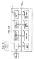
- Fig.5 is a block diagram showing the configuration of the second embodiment of an image processing device according to the present invention.
- a host interface (hereinafter called "host I/F") 101 receives color gradation data, in which characters, graphic forms and natural pictures prepared by a host device (not shown) are mixed, from the host device.
- a frame buffer 121 to 123 store the color gradation data received from the host I/F 101 into R (red), G (green) and B (blue) each for one screen by colors.
- a comparator 103 reads each color gradation data stored in the frame buffers 121 to 123 for each picture element to compare with predetermined values. When the values read from the frame buffers 121, 122 and 123 coincide with the predetermined values, the comparator 103 transmits a signal to an under color removal(UCR) and black generation circuit 104 as mentioned later and a masking circuit 105 as mentioned later to notify the later stage of the coincidence. When not coincided, no signal will be transmitted to the later stage.
- UCR under color removal
- the under color removal and black generation circuit 104 When it has not received a signal showing that the values read from the comparator 103 coincide with the predetermined values, the under color removal and black generation circuit 104 generates data for four colors: C, M, Y and K from each of R, G and B color gradation data, which has been read from the comparator 103, by using the following method.
- K0 min (C0, M0, Y0)
- Each of C, M, Y and K gradation data is determined by the foregoing, and is output to a masking circuit 105 for performing color correction in a later stage.
- the masking circuit 105 for performing color correction receives each of C, M, Y and K gradation data from the under color removal and black generation circuit 104. When it has not received a signal showing that the values read from the comparator 103 coincide with the predetermined values, the masking circuit performs color correction by the following operation to obtain masked signals for C′, M′, Y′ and K′.
- Y, M, C and K are a value for each color read from the under color removal and black generation circuit 104 respectively
- Y′, M′, C′ and K′ are a value for each color after correction respectively.
- a, b, c, d, e, f, g, h, i, and j are predetermined color correction coefficients.
- primary color correction has been performed, but color correction more than primary, that is, non-linear masking may be performed.
- the R.G.B data in the comparator 103 are synchronized with a signal showing that the value read from the comparator 103 coincides with the predetermined value, the R.G.B data will be adequately delayed.
- An interface (I/F) 106 is interface means for transmitting each of Y′, M′, C′ and K′ color values, to a printing device, which have been output from the masking circuit 105.
- a CPU 110 controls the entire apparatus.
- a ROM 111 stores a program, etc. based on the flow charts in Figs.6A to 6C as mentioned later, and a RAM 112 is used as a work area for various programs.
- Fig.6A is a flow chart of assistance in explaining the data procedure for comparison based on the second embodiment.
- the comparator 103 reads (step S101) each of R, G and B data from the frame buffers 121, 122 and 123. Then each of R, G and B data, which have been read in step S101, is compared with the predetermined values (step S102). As a result, after coincidence has been confirmed, the process proceeds to step S103, and when, on the other hand, coincidence could not be confirmed, the process proceeds to step S104.
- step S103 a signal showing that the values read from the frame buffers 121, 122 and 123 in step S101 coincide with the predetermined values, is transmitted to the under color removal and black generation circuit 104 and masking circuit 105.
- the process proceeds to step S104, and each of R, G and B data, which has been read in step S101, is transmitted to the under color removal and black generation circuit 104.
- the process returns to step S101 again to repeat the above operations.
- Fig.6B is a flow chart of assistance in explaining the data procedure for the under color removal and black generation in the second embodiment.
- each of R, G and B data is read from the comparator 103 by the under color removal and black generation circuit 104 (step S111). Then it is checked (step S112) whether or not a coincidence signal showing that the values read from the frame buffers 121, 122 and 123 coincide with the predetermined values, has been input from the comparator 103.
- step S113 when it is confirmed that the coincidence signal has been input, the process proceeds to the next step S113.
- step S114 When it is confirmed that a non-coincidence signal has been input, the process skips to step S114.
- step S103 obtain complements on each of the input R, G and B data, regard as C, M and Y values respectively, and further set the K value to 0.
- the process proceeds to the next step S115.
- step S114 perform the under color removal and black generation by using the above-mentioned method in step S114 to perform a process for obtaining each of C, M, Y and K values.
- step S115 C, M, Y and K values obtained in step S113 or step S114 are transmitted to the masking circuit 105 to correct the color. The process returns to step S111 again to repeat the above operations.
- step S101 When the values read from the frame buffers 121, 122 and 123 in step S101 coincide with the predetermined values in the comparator 103 from the above process, the under color removal and black generation are not performed, but Y, M, C and K are determined in accordance with a specified algorithm.
- Fig.6C is a flow chart of assistance in explaining the data procedure for the color correction using the CPU 110 in the second embodiment.
- each of C, M, Y and K data is read from the under color removal and black generation circuit 104 by the masking circuit 105 (step S121). Then it is checked (step S122) whether or not a coincidence signal showing that the data values read from the frame buffers 121,122 and 123 coincide with the predetermined values, has been input from the comparator 103.
- step S123 the values predetermined by each of the input C, M, Y and k data values are set to C′, M′, Y′ and K′ values respectively.
- step S125 the values predetermined by each of the input C, M, Y and k data values are set to C′, M′, Y′ and K′ values respectively. The process proceeds to step S125.
- step S124 C′, M′, Y′ and K′ values are obtained, which have been color corrected in the masking circuit 105 by using the above-mentioned method.
- step S125 each of C′, M′, Y′ and K′ values obtained in the above step S123 or step S124 is transmitted to the I/F 106. The process returns to step S121 again to repeat the above operations.
- the image from the I/F 106 is output to a printer, CRT, etc., or an external communication function through a public circuit or digital circuit can be added by connecting a communication process circuit to the I/F 106.
- a printer in Fig.8 can be used like the above-mentioned embodiment.
- the above process may be performed using a computer software without providing a special hardware.
- the third embodiment will be explained.
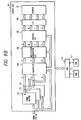
- Fig.7 is a block diagram showing the configuration of the third embodiment of an image processing apparatus according to the present invention.
- the frame buffers 21, 22 and 23 are omitted which are shown in the second embodiment in Fig.5. That is, a configuration is shown in which color gradation data for one screen for each of R, G and B are prepared on the host device side and are input into the apparatus through the host I/F 101 for each picture element in the order of R, G and B.
- the third embodiment has the same configuration as the second embodiment except frame buffers 121, 122 and 123, and the same numbers are assigned.
- the explanation is omitted.
- This embodiment is effective not for such a laser beam printer with high image forming speed as shown in Fig.8, but for the above bubble jet type printer, for example, which prints at a comparatively low speed.
- no frame buffer is required for a printer or printer interface, but only a buffer for several lines at most is required. Therefore the circuit configuration can be simplified to reduce the cost.
- an unnecessary image process can be eliminated in accordance with the input image, and an image process suitable for the feature of an input image can be performed at high speed.
- the host I/F 101 in the above second embodiment can have the same configuration as in the first embodiment.
- Fig.9 shows such a configuration.
- a printer 107 is for reproduction of an image.
- Character data, graphic data (painting command), and bit map data (image data for each picture element read by a scanner, for example, or prepared by a computer graphic) are transmitted from the host computer 1 to the host I/F.
- the data are described in PDL (Page Description Language) such as Post Script (trademark).
- Data transmitted from the host computer 1 is accumulated in a buffer memory 30, and it is identified in a command analysis unit 27 whether the data is (i) character data or graphic data, or (ii) bit map data. This identification data is input into the comparator 103 through a data bus 25.
- the identification data is output corresponding to the picture element to be read from the frame buffers 121 to 123, and when it is read from the buffer by raster scanning, for example, it is output by raster scanning.
- the command analysis unit has a bit map memory for one screen, and stores the identification data for each picture element beforehand.
Abstract
Description
- The present invention relates to an image processing apparatus and, more particularly to an image processing apparatus for processing image data with color information.
- A conventional color printing apparatus was so constructed that a predetermined color reproduction process is performed, and had not any other operation modes which simplify the color reproduction process for printing.
- Accordingly, when the predetermined color reproduction process is complicated, there were the following defects especially in processing color image data in the above conventional example:
- (1) It takes time to paint because a complicated process should be repeated.
- (2) The color tone of the obtained picture often does not conform to the desired one, but requires a color correction process. The desired painting result is usually not obtained once.
- Conventionally in this type of apparatus, there was a color correction processing device for an apparatus for recording color information such as an ink jet type or an electrophotography type.
- As the color correction method in such an apparatus, a method for a masking process whereby an image on a CRT screen or scanner draft image is color matched with a recording image on a recording medium, or a black generation and under color removal (UCR) method for inking on a recording image, etc. are known.
- In the above conventional example, however, a natural picture is mainly processed, and therefore even for an object image, in which characters and graphic forms prepared by a computer are mixed with the natural picture, a color correction process similar to the above-mentioned process is performed. In this case, the conventional example had a defect that the masking, black generation, under color removal, etc. are performed also for characters, which should be originally recorded all in black, and graphic forms, which should be painted out in a color specified by a color sample.
- On the other hand, a technique, that detects a black edge in image data, which have been input from a reader, and prints unmasked black data on that black edge, is disclosed by U.S. Patent Application S.N. 267,366. However, there was room for improvement in the detection method, etc. of the black edge.
- Also a technique, that selects whether or not the masking and under color removal process should be performed in accordance with the input command data, is disclosed by U.S. Patent Application S.N. 298,352. However, there was room for improvement in the mode selection, etc.
- It is an object of the present invention to provide an image processing apparatus and method that solved the above-mentioned problems at issue, that is, to provide a color image forming apparatus, which has been so constructed that the color reproduction procedure can be simplified as required.
- It is a further object of the present invention to provide an image processing apparatus and method with a good color reproducibility.
- It is also an object of the present invention to speed up the image process.
- It is another object of the present invention to easily draw or paint features of an image.
- The other objects and configuration of the present invention will be clarified by the description referring to the drawings below and in the claims.
-
- Fig.1 is a block diagram showing the first embodiment according to the present invention;
- Fig.2 is a view showing an example of a color reproduction process ;
- Figs.3 and 4 are flow charts showing a process from the time the color data is processed by the selection of a mode until the color print image is output;
- Fig.5 is a block diagram showing the configuration of the second embodiment of an image processing apparatus according to the present invention;
- Fig.6A is a flow chart of assistance in explaining the data procedure for comparison in the second embodiment;
- Fig.6B is a flow chart of assistance in explaining the data procedure for under color removal and black generation in the second embodiment;
- Fig.6C is a flow chart of assistance in explaining the data procedure for color correction using CPU10 in the second embodiment;
- Fig.7 is a block diagram showing the configuration of the third embodiment of an image processing apparatus according to the present invention;
- Fig.8 is a view showing an example of a printer according to the present invention; and
- Fig.9 is a block diagram showing the configuration of the fourth embodiment.
- Fig.1 is a block diagram showing the circuit configuration of a printing apparatus in the first embodiment according to the present invention. The printing apparatus according to this embodiment is composed of a
host computer 1 and theprinting apparatus body 2. - The
host computer 1 transmits print data (character data, graphic data, bit map data), print command (paper size, number of papers, etc.), etc. to theprinting apparatus body 2 to allow thisprinting apparatus body 2 to print. - The
printing apparatus body 2 has a microprocessor system including ROM and RAM. That is, theprinting apparatus body 2 is equipped with aninterface 21 for exchanging data with thehost computer 1, a color reproduction processinformation storage unit 22, in which information such as masking coefficient and gamma correction coefficient, which are required for color reproduction process, are stored, a colorreproduction process unit 23 for actually performing the color reproduction process, anoperation panel 24 for changing and setting parameters for printing environment, adata bus 25, acontrol unit 26 for controlling the apparatus in whole, acommand analysis unit 27 for analyzing the print data, print command, etc. which have been transmitted from thehost computer 1, adot development unit 28 for developing the color image data, which have been formed through the colorreproduction process unit 23, into dot information, and anoutput unit 29 for changing the data, which have been developed in the dot information, into permanent visual image on a recording sheet. Anoutlet 29 consists of a display device, such as a color monitor, capable of forming a color image, a recording device such as an electrophotographic printer, a transmitting device for transmitting an image through a public circuit and LAN, and the like. - Fig.2 shows an example of color reproduction process that is performed by the color
reproduction process unit 23 shown in Fig.1. The illuminated process shows a flow which converts signals for three basic primary colors: R(Red), G(Green) and B(Blue) of color into signals for primary colors of coloring material to be printed: C(Cyan), M(Magenta), Y(Yellow) and BK(Black). - First in a process "1", generate C, M and Y, density information, by performing logarithmic transformation to R, G, and B values, brightness information.
- In a process "2", perform the under color removal process to newly create BK on the basis of C, M and Y values which have been obtained in process "1".
- In a process "3", perform masking to remove effects of the mutual extraneous absorption characteristic in C, M and Y toners or ink.
- In a process "4", adjust (gamma conversion) contrast brightness in accordance with the image.
- In a printing apparatus according to this embodiment, color painting is to be made by selecting either of the following two items:
- ① An ordinary color reproduction process mode, which converts the data of three basic primary colors R, G and B into primary colors C, M, Y and BK of coloring material of the printing apparatus in accordance with an instruction from the host computer 1 (Fig.1), and
- ② "Draft mode" obtained by simplifying the process for an ordinary processing mode.
- Figs.3 and 4 are flow charts showing that the color data is processed by selecting such a mode to output the color printing image.
- First in step S1, the mode is selected by the
host computer 1, and proceed to step S2. - In step S2, read one color data (a set of R, G and B data is regarded as one data), and proceed to step S3.
- If there is no data which have been read in step S3, proceed to step S11 to exaust or discharge paper, and end the process.
- If there exist data which have been read in step S3, proceed to step S4 to check the mode selected in step S1.
- When an ordinary process mode has been selected (step S5 ), sequentially execute color reproduction processes "1" to "4" shown in Fig.2 in step S6, and proceed to step S10.
- On the other hand, when the draft mode has been selected (step S7), execute only a color reproduction process "1" shown in Fig.2 in step S8, and proceed to step S9 to skip over processes "2" to "4", and then proceed to step S10.
- In step S10, develop a color image on a dot development unit 28 (Fig.1) on the basis of C, M, Y and BK values obtained by the color reproduction process, and further return to step S2 to repeat the process until the color data to be read are out.
- As mentioned above, the printing process can be simplified by skipping over the color reproduction process.
- The above-mentioned processes "1" to "4" are performed by the software of a computer, of which the color
reproduction process unit 23 is composed. In such a case, the unnecessary process can be omitted to speed up the process by selecting the above-mentioned draft mode. - Instead of using the software, each of processes "1" to "4" is provided with a well-known density conversion circuit, under color removal (UCR) circuit, masking circuit, and gamma conversion circuit, and in the case of the draft mode, the data may pass through the under color removal circuit, masking circuit, and gamma conversion circuit.
- An example of the
output unit 29 according to this embodiment will be explained referring to Fig.8. Aprinter interface 701 is composed of aframe memory 702 for storing image data, aCPU 703 for reading and writing inmemory 702 or notifying thecontrol unit 26 of end in transferring data and errors, and the like. - Image data stored in the
frame memory 702 are transmitted to acolor printer 704 to modulate the pulse width in a PWM (Pulse Width Modulation)circuit 778. Ascanner 711 has a laser output unit for converting an image signal from thePWM circuit 778 to light signal, apolygon mirror 712, which is a polyhedron (such as an octahedron), a motor (not shown) for rotating thismirror 712, f/ϑ lens (image formation lens) 713, etc. -
Numeral 714 is a reflecting mirror for changing the optical path of laser light, and numeral 715 is a photosensitive drum. Laser light emitted from a laser output unit is reflected on thepolygon mirror 712, and linearly raster scans the surface of aphotosensitive drum 715 through alens 713 and amirror 714 to form a latent image corresponding to the draft (original) image. -
Numeral 711 is a primary electrifier (charger), 718 is a total exposure lamp, and 723 is a cleaner unit for collecting residual toner which has not been transferred.Numeral 724 is a before-transfer electrifier (charger). These members are placed around thephotosensitive drum 715. - A
development counter unit 726 develops an electrostatic latent image formed on the surface of thephotosensitive drum 715 by laser exposure. Developingsleeves photosensitive drum 715 for direct developing.Toner hoppers screw 732 transports developer. Thedevelopment counter unit 726 consists of these sleeves 731Y to 731Bk,toner hoppers 730Y to 730Bk and screw 732, and these members are placed around a rotating shaft P of the development counter unit. - To form a Yellow toner image, for example, perform Yellow toner development at the position in this figure. To form a Magenta toner image, rotate the
development counter unit 726 on a shaft P of the figure to place the developingsleeve 731M within the Magenta development counter at a position in contact with aphotosensitive body 715. Cyan and Black development are similarly performed. - A
transfer drum 716 transfers a toner image formed on thephotosensitive drum 715 on paper, and anactuator plate 719 detects the moving position of atransfer drum 716. Aposition sensor 720 detects that thetransfer drum 716 has moved to the home position by approaching to theactuator plate 719.Numeral 725 is a transfer drum cleaner, 727 is a paper hold-down roller, 728 is a deelectrifier (discharger), and 729 is a tranfer electrifier. Thesemembers transfer roller 729. - On the other hand,
numerals cassettes Numerals transfer drum 716 while its tip is being held by a gripper as mentioned later, and then shifts to the image forming process. - A
drum driving motor 550 synchronously rotates thephotosensitive drum 715 and thetransfer drum 716. Apeel pawl 750 removes the paper from thetransfer drum 716 after completing the image forming process. Aconveyance belt 742 conveys the removed paper. An image fixing unit 743 fixes the paper conveyed by theconveyance belt 742, and has a pair ofthermal pressure rollers - In the above-mentioned embodiments, four processes of the color reproduction process have been cited as examples, but it is needless to say that it is applicable to other processes.
- In the above-mentioned "Draft mode", an example, in which only a process "1" (density conversion) is performed, was described. However, when only processes "1" and "2" are performed, when only processes "1" and "3" are performed, and in some other cases, it is applicable to all combinations of conceivable processes by selecting the process to be skipped over.
- Although a selection of print mode from the host computer has been described in the above-mentioned embodiment, it is also possible to select the print mode from the
operation panel 24 for the printing apparatus. - A color image forming apparatus according to this embodiment can be applied to an output device capable of forming a color image such as a color laser beam printer, color ink jet printer, and color thermal transfer printer. Especially the ink jet printer includes a so-called bubble jet printer using such a type of head as to discharge liquid droplet by film boiling using heat energy. A printer for printing binary data per picture element (pixel) or multivalue data may be used.
- As described above, according to the present invention,
- (1) The overall processing time can be greatly shortened by simplifying a complicated image process.
- (2) This can be used to grasp the outline of a painting result.
- Fig.5 is a block diagram showing the configuration of the second embodiment of an image processing device according to the present invention. In Fig.5, a host interface (hereinafter called "host I/F") 101 receives color gradation data, in which characters, graphic forms and natural pictures prepared by a host device (not shown) are mixed, from the host device. A
frame buffer 121 to 123 store the color gradation data received from the host I/F 101 into R (red), G (green) and B (blue) each for one screen by colors. - A
comparator 103 reads each color gradation data stored in theframe buffers 121 to 123 for each picture element to compare with predetermined values. When the values read from theframe buffers comparator 103 transmits a signal to an under color removal(UCR) andblack generation circuit 104 as mentioned later and amasking circuit 105 as mentioned later to notify the later stage of the coincidence. When not coincided, no signal will be transmitted to the later stage. - When it has not received a signal showing that the values read from the
comparator 103 coincide with the predetermined values, the under color removal andblack generation circuit 104 generates data for four colors: C, M, Y and K from each of R, G and B color gradation data, which has been read from thecomparator 103, by using the following method. - First, obtain complements on the read RGB data as follows:

- Further obtain the minimum values for C₀, M₀ and Y₀, and regard this as K₀.

- Multiply K₀ by a predetermined factor α, and deduct this from C₀, M₀ and Y₀, and then regard as C, M and Y respectively.


- Similarly, multiply K′ by a factor β beforehand, and regard this as K.

- Each of C, M, Y and K gradation data is determined by the foregoing, and is output to a
masking circuit 105 for performing color correction in a later stage. - On the other hand, when it has received a signal showing that the values read from the
comparator 103 coincide with the predetermined values, the under color removal andblack generation circuit 104 outputs each of C, M, Y and K gradation data to themasking circuit 105 at a later stage, assuming as follows:
- The
masking circuit 105 for performing color correction receives each of C, M, Y and K gradation data from the under color removal andblack generation circuit 104. When it has not received a signal showing that the values read from thecomparator 103 coincide with the predetermined values, the masking circuit performs color correction by the following operation to obtain masked signals for C′, M′, Y′ and K′. That is,


black generation circuit 104 respectively, and Y′, M′, C′ and K′ are a value for each color after correction respectively. a, b, c, d, e, f, g, h, i, and j are predetermined color correction coefficients. In the second embodiment, primary color correction has been performed, but color correction more than primary, that is, non-linear masking may be performed. - When it has received a signal showing that the values read from the
comparator 103 coincide with the predetermined values, the masking circuit outputs Y′, M′, C′ and K′ values which were predetermined in accordance with the input Y, M, C and K values. Assuming a number of bits for the color gradation data to be stored in theframe buffers 121 to 123, for example, as 8 bits, when the value read from theseframe buffers - If the
comparator 103 is so set beforehand that a signal is given to the under color removal andblack generation circuit 104 and maskingcircuit 105 when R = G = B = 0, themasking circuit 105 receives a signal from thecomparator 103 when the values read from theframe buffers black generation circuit 104 at this time, it will be possible to record only K (black) if it is so set beforehand that M′ = Y′ = 0 and K = 255 are output when both conditions meet. - Since the R.G.B data in the
comparator 103 are synchronized with a signal showing that the value read from thecomparator 103 coincides with the predetermined value, the R.G.B data will be adequately delayed. - An interface (I/F) 106 is interface means for transmitting each of Y′, M′, C′ and K′ color values, to a printing device, which have been output from the
masking circuit 105. ACPU 110 controls the entire apparatus. AROM 111 stores a program, etc. based on the flow charts in Figs.6A to 6C as mentioned later, and aRAM 112 is used as a work area for various programs. - The operation in the second embodiment will be explained below.
- Fig.6A is a flow chart of assistance in explaining the data procedure for comparison based on the second embodiment.
- It is assumed that each of R, G and B data has already been stored in the
frame buffers 121 to 123 through the host I/F 101. - First, the
comparator 103 reads (step S101) each of R, G and B data from theframe buffers - In step S103, a signal showing that the values read from the
frame buffers black generation circuit 104 and maskingcircuit 105. The process proceeds to step S104, and each of R, G and B data, which has been read in step S101, is transmitted to the under color removal andblack generation circuit 104. The process returns to step S101 again to repeat the above operations. - Fig.6B is a flow chart of assistance in explaining the data procedure for the under color removal and black generation in the second embodiment.
- First, each of R, G and B data is read from the
comparator 103 by the under color removal and black generation circuit 104 (step S111). Then it is checked (step S112) whether or not a coincidence signal showing that the values read from theframe buffers comparator 103. - As a result, when it is confirmed that the coincidence signal has been input, the process proceeds to the next step S113. When it is confirmed that a non-coincidence signal has been input, the process skips to step S114. In step S103, obtain complements on each of the input R, G and B data, regard as C, M and Y values respectively, and further set the K value to 0. The process proceeds to the next step S115.
- On the other hand, perform the under color removal and black generation by using the above-mentioned method in step S114 to perform a process for obtaining each of C, M, Y and K values. In step S115, C, M, Y and K values obtained in step S113 or step S114 are transmitted to the
masking circuit 105 to correct the color. The process returns to step S111 again to repeat the above operations. - When the values read from the
frame buffers comparator 103 from the above process, the under color removal and black generation are not performed, but Y, M, C and K are determined in accordance with a specified algorithm. - Fig.6C is a flow chart of assistance in explaining the data procedure for the color correction using the
CPU 110 in the second embodiment. - First, each of C, M, Y and K data is read from the under color removal and
black generation circuit 104 by the masking circuit 105 (step S121). Then it is checked (step S122) whether or not a coincidence signal showing that the data values read from the frame buffers 121,122 and 123 coincide with the predetermined values, has been input from thecomparator 103. - As a result, when it is confirmed that the coincidence signal has been input, the process proceeds to the next step S123. When it is confirmed that a non-coincidence signal has been input, the process skips to step S124. First, in step S123, the values predetermined by each of the input C, M, Y and k data values are set to C′, M′, Y′ and K′ values respectively. The process proceeds to step S125.
- On the other hand, in step S124, C′, M′, Y′ and K′ values are obtained, which have been color corrected in the
masking circuit 105 by using the above-mentioned method. In step S125, each of C′, M′, Y′ and K′ values obtained in the above step S123 or step S124 is transmitted to the I/F 106. The process returns to step S121 again to repeat the above operations. - For characters, which should be originally recorded all in black, and graphic forms, which should be painted out in a color specified by a color sample, the under color removal, black generation and color correction (masking) are not performed, but can be performed for natural pictures.
- As explained above, an unnecessary image process can be eliminated in accordance with the input image according to the second embodiment.
- The image from the I/
F 106 is output to a printer, CRT, etc., or an external communication function through a public circuit or digital circuit can be added by connecting a communication process circuit to the I/F 106. - For the printer, a printer in Fig.8 can be used like the above-mentioned embodiment.
- The above process may be performed using a computer software without providing a special hardware.
- The third embodiment will be explained.
- Fig.7 is a block diagram showing the configuration of the third embodiment of an image processing apparatus according to the present invention. In Fig.7, the frame buffers 21, 22 and 23 are omitted which are shown in the second embodiment in Fig.5. That is, a configuration is shown in which color gradation data for one screen for each of R, G and B are prepared on the host device side and are input into the apparatus through the host I/
F 101 for each picture element in the order of R, G and B. - The third embodiment has the same configuration as the second embodiment except
frame buffers comparator 103 and after are also the same as in the second embodiment, the explanation is omitted. - This embodiment is effective not for such a laser beam printer with high image forming speed as shown in Fig.8, but for the above bubble jet type printer, for example, which prints at a comparatively low speed. In this embodiment, no frame buffer is required for a printer or printer interface, but only a buffer for several lines at most is required. Therefore the circuit configuration can be simplified to reduce the cost.
- As mentioned above, an unnecessary image process can be eliminated in accordance with the input image, and an image process suitable for the feature of an input image can be performed at high speed.
- The host I/
F 101 in the above second embodiment can have the same configuration as in the first embodiment. Fig.9 shows such a configuration. In the same configurations as in Figs.1 and 5, the same numbers are assigned. Aprinter 107 is for reproduction of an image. - The operation of an image processing apparatus in Fig.9 will be explained.
- Character data, graphic data (painting command), and bit map data (image data for each picture element read by a scanner, for example, or prepared by a computer graphic) are transmitted from the
host computer 1 to the host I/F. The data are described in PDL (Page Description Language) such as Post Script (trademark). - Data transmitted from the
host computer 1 is accumulated in abuffer memory 30, and it is identified in acommand analysis unit 27 whether the data is (i) character data or graphic data, or (ii) bit map data. This identification data is input into thecomparator 103 through adata bus 25. - The identification data is output corresponding to the picture element to be read from the
frame buffers 121 to 123, and when it is read from the buffer by raster scanning, for example, it is output by raster scanning. For this reason, the command analysis unit has a bit map memory for one screen, and stores the identification data for each picture element beforehand. When overwriting in PDL with such a configuration, the identification data for an image, which becomes a top when it is changed into a visible image, can be transmitted to thecomparator 103. - In the
comparator 103, when the above identification data is (i) character data or graphic data, the same process as in the second embodiment is performed, but in the case of bit map data, a process using the under color removal andblack generation circuit 104 or maskingcircuit 105 is performed even if the image data is equal to the predetermined value (e.g., R = G = B = D). This is because if the under color removal and masking are not performed only for the black picture element of the natural picture, the color balance will be lost and the picture element portion is likely to become unnatural in the entire image, and it should be prevented. - The present invention is not limited to the above embodiments, but can be applied by modifying in various ways within the scope of the claims.
Claims (31)
- An image processing apparatus, comprising:
judgement means which judges whether or not an input color image data is a specific value;
color correction means which color corrects said input color image data; and
control means which controls color correction by said color correction means in accordance with judgement by said judgement means,
wherein said control means ensures that color correction is not performed by said color correction means when the input image data has been judged by said judgement means to be a specific value. - The image processing apparatus according to Claim 1, wherein said judgement means judges whether or not the input color image data represents a specific color.
- The image processing apparatus according to Claim 2, wherein said specific color is black.
- The image processing apparatus according to Claim 1, wherein said color correction means performs a masking process.
- The image processing apparatus according to Claim 1, wherein said color correction means performs a gamma conversion.
- The image processing apparatus according to Claim 1, wherein said color correction is performed by a computer software.
- The image processing apparatus according to Claim 1, wherein said color correction is performed by a hardware.
- An image processing method, comprising the following steps:
a judgement step which judges whether or not an input color image data is a specific value;
a color correction step which color corrects the input color image data; and
a selection step which selects either a first mode for performing said color correction or a second mode for not performing said color correction in accordance with the judgement in said judgement step. - The image processing method according to Claim 8, wherein said judgement step judges whether or not an input image data represents a specific color.
- The image processing method according to Claim 9, wherein said specific color is black.
- The image processing method according to Claim 8, wherein said color correction step performs masking.
- The image processing method according to Claim 8, wherein said color correction step performs gamma conversion.
- The image processing method according to Claim 8, wherein said color correction is performed by a computer software.
- The image processing method according to Claim 8, wherein said color correction is performed by a hardware.
- An image processing method, comprising the following steps:
a development step which analyzes a received command data and develops into an image;
a judgement step which judges whether or not an image developed in accordance with said command data is an image data for each picture element; and
a selection step which selects either a first mode for performing color correction or a second mode for not performing color correction in accordance with the judgement in said judgement step. - The image processing method according to Claim 15, wherein said analysis step analyzes which said command data includes among character data, graphic data and bit map data.
- The image processing method according to Claim 15, wherein said judgement step judges in accordance with the command data.
- The image processing method according to Claim 15, having a step to store a result further judged by judgement step.
- The image processing method according to Claim 15, wherein said selection step selects the first mode when an image to be developed has been judged to be an image data for each picture element.
- The image processing method according to Claim 15, wherein said color correction is masking.
- The image processing method according to Claim 15, wherein said color correction is gamma conversion.
- The image processing method according to Claim 15, wherein said color correction is performed by a computer software.
- The image processing method according to Claim 15, wherein said color correction is performed by a hardware.
- An image processing method, comprising the following steps:
an input step which inputs red, green and blue component signals;
a judgement step which judges whether or not the level of the red green and blue component signals is zero; and
a color correction step which color corrects input signals in accordance with said judgement. - The image processing method according to Claim 24, wherein said color correction step performs masking.
- The image processing method according to Claim 24, wherein said color correction step performs gamma conversion.
- The image processing apparatus according to Claim 24, wherein said color correction is performed by a computer software.
- The image processing apparatus according to Claim 24, wherein said color correction is performed by a hardware.
- Colour image processing means having first and second modes of operation which may be selected, the processing means performing a plurality of processing steps on colour image data in the first mode, and not performing some of the said steps on the colour image data in the second mode.
- Colour image processing means according to claim 29 in which the selection of the mode of operation is made at least partly on the basis of colour value data in the colour image data.
- Colour image processing means according to claim 29 or claim 30 in which the selection of the mode of operation is made at least partly on the basis of a signal not representing colour value data in the colour image signal.
Priority Applications (1)
| Application Number | Priority Date | Filing Date | Title |
|---|---|---|---|
| EP96200033A EP0720349B1 (en) | 1990-03-06 | 1991-03-05 | Image processing apparatus and method |
Applications Claiming Priority (4)
| Application Number | Priority Date | Filing Date | Title |
|---|---|---|---|
| JP2052651A JP2831784B2 (en) | 1990-03-06 | 1990-03-06 | Color image processing method |
| JP52651/90 | 1990-03-06 | ||
| JP161389/90 | 1990-06-21 | ||
| JP2161389A JPH0453348A (en) | 1990-06-21 | 1990-06-21 | Picture processing unit |
Related Child Applications (2)
| Application Number | Title | Priority Date | Filing Date |
|---|---|---|---|
| EP96200033.7 Division-Into | 1991-03-05 | ||
| EP96200033A Division EP0720349B1 (en) | 1990-03-06 | 1991-03-05 | Image processing apparatus and method |
Publications (3)
| Publication Number | Publication Date |
|---|---|
| EP0446019A2 true EP0446019A2 (en) | 1991-09-11 |
| EP0446019A3 EP0446019A3 (en) | 1992-08-26 |
| EP0446019B1 EP0446019B1 (en) | 1996-11-13 |
Family
ID=26393281
Family Applications (2)
| Application Number | Title | Priority Date | Filing Date |
|---|---|---|---|
| EP91301823A Expired - Lifetime EP0446019B1 (en) | 1990-03-06 | 1991-03-05 | Image processing apparatus and method |
| EP96200033A Expired - Lifetime EP0720349B1 (en) | 1990-03-06 | 1991-03-05 | Image processing apparatus and method |
Family Applications After (1)
| Application Number | Title | Priority Date | Filing Date |
|---|---|---|---|
| EP96200033A Expired - Lifetime EP0720349B1 (en) | 1990-03-06 | 1991-03-05 | Image processing apparatus and method |
Country Status (6)
| Country | Link |
|---|---|
| US (1) | US5457549A (en) |
| EP (2) | EP0446019B1 (en) |
| KR (1) | KR950011066B1 (en) |
| CN (2) | CN1029264C (en) |
| DE (2) | DE69123067T2 (en) |
| ES (1) | ES2093678T3 (en) |
Families Citing this family (8)
| Publication number | Priority date | Publication date | Assignee | Title |
|---|---|---|---|---|
| DE69430464T2 (en) * | 1993-09-29 | 2002-10-31 | Canon Kk | Image processing device and method |
| JPH09270928A (en) | 1996-04-02 | 1997-10-14 | Canon Inc | Image processor and image processing method |
| US5995724A (en) * | 1996-11-01 | 1999-11-30 | Mikkelsen; Carl | Image process system and process using personalization techniques |
| US6269190B1 (en) * | 1996-09-24 | 2001-07-31 | Electronics For Imaging, Inc. | Computer system for processing images using a virtual frame buffer |
| JPH10224551A (en) * | 1997-01-31 | 1998-08-21 | Canon Inc | Image processor and its method |
| US7369269B2 (en) * | 2000-11-29 | 2008-05-06 | Hewlett-Packard Development Company, L.P. | Print toner density mode/print media default link |
| JP2008165381A (en) * | 2006-12-27 | 2008-07-17 | Ricoh Co Ltd | Image processing device and image processing method |
| JP6071973B2 (en) * | 2014-10-09 | 2017-02-01 | キヤノン株式会社 | Information processing apparatus, control method, and program |
Citations (5)
| Publication number | Priority date | Publication date | Assignee | Title |
|---|---|---|---|---|
| DE3417188A1 (en) * | 1983-05-10 | 1984-11-15 | Canon K.K., Tokio/Tokyo | Method and system for colour image reproduction |
| EP0323265A2 (en) * | 1987-12-29 | 1989-07-05 | Canon Kabushiki Kaisha | Method of processing color image and apparatus therefor |
| US4862255A (en) * | 1986-12-16 | 1989-08-29 | Victor Company Of Japan, Ltd. | Color correcting circuit for thermal printer selectively outputting a second degree correction operation result and a modified result thereof |
| US4893180A (en) * | 1985-11-09 | 1990-01-09 | Fuji Photo Film Co., Ltd. | Color image signal processing method |
| US4989079A (en) * | 1987-10-23 | 1991-01-29 | Ricoh Company, Ltd. | Color correction device and method having a hue area judgement unit |
Family Cites Families (5)
| Publication number | Priority date | Publication date | Assignee | Title |
|---|---|---|---|---|
| US4418358A (en) * | 1980-11-07 | 1983-11-29 | Robert Bosch Gmbh | Method and system to correct color errors in color television signals generated by scanning a film |
| US4974067A (en) * | 1986-06-06 | 1990-11-27 | Ricoh Company, Ltd. | Multi-step-digital color image reproducing method and apparatus |
| DE3750860T3 (en) * | 1986-08-13 | 1999-10-14 | Canon Kk | Method and device for processing color images. |
| DE3839299C2 (en) * | 1987-11-20 | 1995-06-01 | Canon Kk | Image processing device |
| JP3048151B2 (en) * | 1988-01-19 | 2000-06-05 | キヤノン株式会社 | Color image forming equipment |
-
1991
- 1991-03-05 CN CN91101338A patent/CN1029264C/en not_active Expired - Fee Related
- 1991-03-05 EP EP91301823A patent/EP0446019B1/en not_active Expired - Lifetime
- 1991-03-05 DE DE69123067T patent/DE69123067T2/en not_active Expired - Lifetime
- 1991-03-05 ES ES91301823T patent/ES2093678T3/en not_active Expired - Lifetime
- 1991-03-05 DE DE69132225T patent/DE69132225T2/en not_active Expired - Lifetime
- 1991-03-05 EP EP96200033A patent/EP0720349B1/en not_active Expired - Lifetime
- 1991-03-06 KR KR1019910003596A patent/KR950011066B1/en not_active IP Right Cessation
-
1994
- 1994-06-04 CN CN94106508A patent/CN1102005C/en not_active Expired - Fee Related
-
1995
- 1995-01-31 US US08/380,938 patent/US5457549A/en not_active Expired - Lifetime
Patent Citations (5)
| Publication number | Priority date | Publication date | Assignee | Title |
|---|---|---|---|---|
| DE3417188A1 (en) * | 1983-05-10 | 1984-11-15 | Canon K.K., Tokio/Tokyo | Method and system for colour image reproduction |
| US4893180A (en) * | 1985-11-09 | 1990-01-09 | Fuji Photo Film Co., Ltd. | Color image signal processing method |
| US4862255A (en) * | 1986-12-16 | 1989-08-29 | Victor Company Of Japan, Ltd. | Color correcting circuit for thermal printer selectively outputting a second degree correction operation result and a modified result thereof |
| US4989079A (en) * | 1987-10-23 | 1991-01-29 | Ricoh Company, Ltd. | Color correction device and method having a hue area judgement unit |
| EP0323265A2 (en) * | 1987-12-29 | 1989-07-05 | Canon Kabushiki Kaisha | Method of processing color image and apparatus therefor |
Also Published As
| Publication number | Publication date |
|---|---|
| CN1054679A (en) | 1991-09-18 |
| US5457549A (en) | 1995-10-10 |
| DE69132225T2 (en) | 2000-10-26 |
| CN1029264C (en) | 1995-07-05 |
| CN1122554A (en) | 1996-05-15 |
| DE69132225D1 (en) | 2000-06-29 |
| EP0720349A1 (en) | 1996-07-03 |
| EP0720349B1 (en) | 2000-05-24 |
| EP0446019B1 (en) | 1996-11-13 |
| ES2093678T3 (en) | 1997-01-01 |
| KR910017319A (en) | 1991-11-05 |
| KR950011066B1 (en) | 1995-09-27 |
| DE69123067D1 (en) | 1996-12-19 |
| EP0446019A3 (en) | 1992-08-26 |
| CN1102005C (en) | 2003-02-19 |
| DE69123067T2 (en) | 1997-03-27 |
Similar Documents
| Publication | Publication Date | Title |
|---|---|---|
| US7855801B2 (en) | Color image forming apparatus and image output method | |
| US6172771B1 (en) | Image forming system and calibration method for image forming conditions | |
| JP4366089B2 (en) | Image forming apparatus and method | |
| JP3703162B2 (en) | Image forming apparatus | |
| EP0446019B1 (en) | Image processing apparatus and method | |
| US6233062B1 (en) | Image processing device and image forming apparatus | |
| US5309548A (en) | Pattern generating method and apparatus | |
| US6048116A (en) | Method and apparatus for drawing characters for display in a draft mode and a high resolution mode | |
| US5777750A (en) | Image processing method and apparatus which includes a color reversing function for a two-color image | |
| JP2001352459A (en) | Image-forming device | |
| US7920288B2 (en) | Image forming apparatus, image forming method and program | |
| AU638804B2 (en) | Image processing apparatus and method | |
| JP4687593B2 (en) | Image processing apparatus and program | |
| JPH1065918A (en) | Image forming device and image processing unit | |
| JPH0662249A (en) | Color image recorder | |
| KR950011067B1 (en) | Method and apparatus for image processing | |
| JP2006243574A (en) | Image forming method and image forming apparatus | |
| GB2359146A (en) | Reduced hot offset in colour electrophotography | |
| US7746499B2 (en) | Color image processing apparatus and method | |
| JP3320093B2 (en) | Image processing apparatus and image processing method | |
| JP2005341417A (en) | Image processing apparatus, storage medium, image scanner, and image forming apparatus | |
| JPH1141446A (en) | Device and method for processing image and recording medium | |
| JPH02295766A (en) | Imaging system | |
| EP0395202B1 (en) | Output apparatus | |
| JP2001103278A (en) | Image forming device |
Legal Events
| Date | Code | Title | Description |
|---|---|---|---|
| PUAI | Public reference made under article 153(3) epc to a published international application that has entered the european phase |
Free format text: ORIGINAL CODE: 0009012 |
|
| AK | Designated contracting states |
Kind code of ref document: A2 Designated state(s): BE DE ES FR GB IT NL |
|
| PUAL | Search report despatched |
Free format text: ORIGINAL CODE: 0009013 |
|
| AK | Designated contracting states |
Kind code of ref document: A3 Designated state(s): BE DE ES FR GB IT NL |
|
| 17P | Request for examination filed |
Effective date: 19930114 |
|
| 17Q | First examination report despatched |
Effective date: 19941007 |
|
| GRAH | Despatch of communication of intention to grant a patent |
Free format text: ORIGINAL CODE: EPIDOS IGRA |
|
| GRAH | Despatch of communication of intention to grant a patent |
Free format text: ORIGINAL CODE: EPIDOS IGRA |
|
| GRAA | (expected) grant |
Free format text: ORIGINAL CODE: 0009210 |
|
| AK | Designated contracting states |
Kind code of ref document: B1 Designated state(s): BE DE ES FR GB IT NL |
|
| DX | Miscellaneous (deleted) | ||
| REF | Corresponds to: |
Ref document number: 69123067 Country of ref document: DE Date of ref document: 19961219 |
|
| REG | Reference to a national code |
Ref country code: ES Ref legal event code: FG2A Ref document number: 2093678 Country of ref document: ES Kind code of ref document: T3 |
|
| ET | Fr: translation filed | ||
| ITF | It: translation for a ep patent filed |
Owner name: SOCIETA' ITALIANA BREVETTI S.P.A. |
|
| PLBE | No opposition filed within time limit |
Free format text: ORIGINAL CODE: 0009261 |
|
| STAA | Information on the status of an ep patent application or granted ep patent |
Free format text: STATUS: NO OPPOSITION FILED WITHIN TIME LIMIT |
|
| 26N | No opposition filed | ||
| REG | Reference to a national code |
Ref country code: GB Ref legal event code: IF02 |
|
| PGFP | Annual fee paid to national office [announced via postgrant information from national office to epo] |
Ref country code: ES Payment date: 20090205 Year of fee payment: 19 |
|
| PGFP | Annual fee paid to national office [announced via postgrant information from national office to epo] |
Ref country code: NL Payment date: 20090318 Year of fee payment: 19 |
|
| PGFP | Annual fee paid to national office [announced via postgrant information from national office to epo] |
Ref country code: BE Payment date: 20090302 Year of fee payment: 19 |
|
| PGFP | Annual fee paid to national office [announced via postgrant information from national office to epo] |
Ref country code: IT Payment date: 20090312 Year of fee payment: 19 |
|
| PGFP | Annual fee paid to national office [announced via postgrant information from national office to epo] |
Ref country code: FR Payment date: 20090325 Year of fee payment: 19 |
|
| PGFP | Annual fee paid to national office [announced via postgrant information from national office to epo] |
Ref country code: GB Payment date: 20100309 Year of fee payment: 20 |
|
| PGFP | Annual fee paid to national office [announced via postgrant information from national office to epo] |
Ref country code: DE Payment date: 20100331 Year of fee payment: 20 |
|
| BERE | Be: lapsed |
Owner name: *CANON K.K. Effective date: 20100331 |
|
| REG | Reference to a national code |
Ref country code: NL Ref legal event code: V1 Effective date: 20101001 |
|
| REG | Reference to a national code |
Ref country code: FR Ref legal event code: ST Effective date: 20101130 |
|
| PG25 | Lapsed in a contracting state [announced via postgrant information from national office to epo] |
Ref country code: NL Free format text: LAPSE BECAUSE OF NON-PAYMENT OF DUE FEES Effective date: 20101001 Ref country code: FR Free format text: LAPSE BECAUSE OF NON-PAYMENT OF DUE FEES Effective date: 20100331 |
|
| PG25 | Lapsed in a contracting state [announced via postgrant information from national office to epo] |
Ref country code: BE Free format text: LAPSE BECAUSE OF NON-PAYMENT OF DUE FEES Effective date: 20100331 |
|
| REG | Reference to a national code |
Ref country code: DE Ref legal event code: R071 Ref document number: 69123067 Country of ref document: DE |
|
| REG | Reference to a national code |
Ref country code: GB Ref legal event code: PE20 Expiry date: 20110304 |
|
| PG25 | Lapsed in a contracting state [announced via postgrant information from national office to epo] |
Ref country code: IT Free format text: LAPSE BECAUSE OF NON-PAYMENT OF DUE FEES Effective date: 20100305 |
|
| REG | Reference to a national code |
Ref country code: ES Ref legal event code: FD2A Effective date: 20110418 |
|
| PG25 | Lapsed in a contracting state [announced via postgrant information from national office to epo] |
Ref country code: ES Free format text: LAPSE BECAUSE OF NON-PAYMENT OF DUE FEES Effective date: 20110404 Ref country code: GB Free format text: LAPSE BECAUSE OF EXPIRATION OF PROTECTION Effective date: 20110304 |
|
| PG25 | Lapsed in a contracting state [announced via postgrant information from national office to epo] |
Ref country code: ES Free format text: LAPSE BECAUSE OF NON-PAYMENT OF DUE FEES Effective date: 20100306 |
|
| PG25 | Lapsed in a contracting state [announced via postgrant information from national office to epo] |
Ref country code: DE Free format text: LAPSE BECAUSE OF EXPIRATION OF PROTECTION Effective date: 20110305 |