EP0445777A2 - Liquid crystal display device - Google Patents
Liquid crystal display device Download PDFInfo
- Publication number
- EP0445777A2 EP0445777A2 EP91103419A EP91103419A EP0445777A2 EP 0445777 A2 EP0445777 A2 EP 0445777A2 EP 91103419 A EP91103419 A EP 91103419A EP 91103419 A EP91103419 A EP 91103419A EP 0445777 A2 EP0445777 A2 EP 0445777A2
- Authority
- EP
- European Patent Office
- Prior art keywords
- liquid crystal
- electrode
- electrodes
- display device
- aperture
- Prior art date
- Legal status (The legal status is an assumption and is not a legal conclusion. Google has not performed a legal analysis and makes no representation as to the accuracy of the status listed.)
- Granted
Links
Images


Classifications
-
- G—PHYSICS
- G02—OPTICS
- G02F—OPTICAL DEVICES OR ARRANGEMENTS FOR THE CONTROL OF LIGHT BY MODIFICATION OF THE OPTICAL PROPERTIES OF THE MEDIA OF THE ELEMENTS INVOLVED THEREIN; NON-LINEAR OPTICS; FREQUENCY-CHANGING OF LIGHT; OPTICAL LOGIC ELEMENTS; OPTICAL ANALOGUE/DIGITAL CONVERTERS
- G02F1/00—Devices or arrangements for the control of the intensity, colour, phase, polarisation or direction of light arriving from an independent light source, e.g. switching, gating or modulating; Non-linear optics
- G02F1/01—Devices or arrangements for the control of the intensity, colour, phase, polarisation or direction of light arriving from an independent light source, e.g. switching, gating or modulating; Non-linear optics for the control of the intensity, phase, polarisation or colour
- G02F1/13—Devices or arrangements for the control of the intensity, colour, phase, polarisation or direction of light arriving from an independent light source, e.g. switching, gating or modulating; Non-linear optics for the control of the intensity, phase, polarisation or colour based on liquid crystals, e.g. single liquid crystal display cells
- G02F1/133—Constructional arrangements; Operation of liquid crystal cells; Circuit arrangements
- G02F1/1333—Constructional arrangements; Manufacturing methods
- G02F1/1343—Electrodes
- G02F1/134309—Electrodes characterised by their geometrical arrangement
- G02F1/134336—Matrix
-
- G—PHYSICS
- G02—OPTICS
- G02F—OPTICAL DEVICES OR ARRANGEMENTS FOR THE CONTROL OF LIGHT BY MODIFICATION OF THE OPTICAL PROPERTIES OF THE MEDIA OF THE ELEMENTS INVOLVED THEREIN; NON-LINEAR OPTICS; FREQUENCY-CHANGING OF LIGHT; OPTICAL LOGIC ELEMENTS; OPTICAL ANALOGUE/DIGITAL CONVERTERS
- G02F1/00—Devices or arrangements for the control of the intensity, colour, phase, polarisation or direction of light arriving from an independent light source, e.g. switching, gating or modulating; Non-linear optics
- G02F1/01—Devices or arrangements for the control of the intensity, colour, phase, polarisation or direction of light arriving from an independent light source, e.g. switching, gating or modulating; Non-linear optics for the control of the intensity, phase, polarisation or colour
- G02F1/13—Devices or arrangements for the control of the intensity, colour, phase, polarisation or direction of light arriving from an independent light source, e.g. switching, gating or modulating; Non-linear optics for the control of the intensity, phase, polarisation or colour based on liquid crystals, e.g. single liquid crystal display cells
- G02F1/133—Constructional arrangements; Operation of liquid crystal cells; Circuit arrangements
- G02F1/1333—Constructional arrangements; Manufacturing methods
- G02F1/1337—Surface-induced orientation of the liquid crystal molecules, e.g. by alignment layers
- G02F1/133707—Structures for producing distorted electric fields, e.g. bumps, protrusions, recesses, slits in pixel electrodes
Definitions
- This invention relates to a liquid crystal display device, and more particularly to a dot matrix type liquid crystal display device adapted for displaying arbitrary shape on a display surface.
- CSH color super homeotropic liquid crystal display
- LCD liquid crystal display
- homeotropically or substantially homeotropically oriented nematic liquid crystal molecules are electrically controlled their birefringence to achieve a desired display.
- a liquid crystal molecule 10 has an elongated shape, and has a higher optical constant (refractive index) along the long axis. Further, the liquid crystal molecule has an electric bipole along a direction orthogonal to the long axis. In the "off" state where an electric field above a certain value is not applied between the electrodes, the liquid crystal molecules take a homeotropic orientation where the long axis is normal to the surface of the substrate, as shown in the left part of the figure. When an electric field E is applied normal to the substrate, there occurs a force in a direction which drives the electric dipole of the liquid crystal molecules to follow the direction of the electric field and the liquid crystal molecule 10 is tilted as shown in the right part of the figure. This angle of tilt is called tilt angle, and is of the order of 10 degrees, for example.
- Fig. 2B shows an electric field distribution in the electrode crossing portion in the liquid crystal display device.
- a pair of glass substrates 11 and 12 are disposed parallel to face each other.
- segment electrodes 1a and 1b and common electrode 2 are formed in a crossing relation.
- the common electrode 2 defines the row of the dot matrix and the segment electrodes 1a and 1b define the column of the dot matrix.
- crossed polarizers 13 and 14 are disposed on the outer surfaces of the glass substrate 11 and 12.
- the electric force line starting form the edge of the segment electrode 1a or 1b is bulged towards the common electrode 2 as shown by the broken line in the figure to have a lateral or horizontal component as well as the vertical component.
- the liquid crystal molecule changes its tilt according to the electric field distribution.
- Fig. 2C shows schematically how the liquid crystal molecules are distributed in the electrode crossing area 5.
- the electrode crossing area 5 is defined between the vertical facing edges 6a and 6b and between the horizontal facing edges 7a and 7b. Since the common electrode 2 extends long in the horizontal direction, the electric force line at the facing edges 6a and 6b, starting from the edges of the segment electrodes 1a and 1b are diverged outwardly as shown by the arrow. Since the segment electrodes 1a and 1b extend long the vertical direction, the electric force line at the horizontal facing edges 7a and 7b of the electrode crossing area 5, starting from the segment electrode are distributed to be oriented from the outside to the inside.
- the polarization axes P1 and P2 of the crossed polarizers are disposed at angles 45 degrees slanted from both the row and the column as shown in the right part of the figure.
- the liquid crystal molecule has a function of rotating the polarized light when tilted from the normal direction, but those liquid crystal molecules which slanted in the direction of the polarization axes P1 and P2 have no such function. Therefore, the light is cut off by the crossed polarizers.
- the electrode crossing area 5 is divided into four regions D1, D2, D3 and D4.
- the liquid crystal molecules are kept normal to the substrates 11 and 12 as shown in Fig. 2B.
- the liquid crystal molecules are tilted in the direction of the polarization axis P1 or P2.
- the liquid crystal molecules are tilted substantially leftward, rightward, upward and downward, respectively, as shown in Fig. 2D.
- the shapes and the areas of the four regions D1, D2, D3 and D4 divided by the crossing black lines vary according to the balance of the various condition, are not constant and differ from cell to cell.
- a preliminary pre-tilt angle in a certain direction may be given to the liquid crystal molecules.
- a pre-tilt angle of not more than one degree in a direction corresponding to the region D3 is given to the liquid crystal molecules in the whole electrode crossing area, almost all the liquid crystal molecules will be tilted in the same direction when an electric field is applied. Then, the most part of the electrode crossing area 5 will be occupied by the region D3. Namely, other three regions D1, D2 and D4 become extremely small areas in the display and the quality of display is greatly improved.
- a pre-tilt is given to control the orientation direction of the liquid crystal molecules, another problem arises.
- the shapes and the positions of the crossing black lines in the display area vary uncertainly to cause a problem in the display performance, or there arises a direction near the normal to the display surface in which the display quality is extremely low.
- An object of this invention is to provide a liquid crystal display device capable of performing display of substantially uniform and good quality in the most part of the electrode crossing area.
- a dot matrix type liquid crystal display device comprising, a pair of parallel substrates disposed to face each other, two groups of electrodes disposed on said pair of substrates, respectively, and crossing each other when projected normal to one of said substrates, each electrode being elongated and having substantially parallel side edges, at least one elongated aperture formed in one electrode of one of said two groups of electrodes at a portion crossing another electrode of the other group of electrodes along the side edges of said another electrode.
- the lateral component of the electric field due to the edge of the electrode crossing area can be positively utilized.
- the shape and the areas of the display regions are uncertain.
- the electrode crossing area can be divided almost into two major regions. In each major region, the electric field is tilted in a constant direction to enable uniform display.
- Figs. 1A, 1B and 1C show basic embodiments of this invention.
- Fig. 1A is a plan view of the first structure.
- Fig. 1B is a plan view of the second structure.
- Fig. 1C is a cross section for showing the electric field distribution in the cell schematically
- Figs. 2A, 2B, 2C and 2D show the prior art.
- Fig. 2A is a schematic cross section showing the liquid crystal molecule.
- Fig. 2B is a schematic cross section for showing the orientation of the liquid crystal molecules in the electrode crossing area.
- Fig. 2C is a schematic plan view for illustrating the orientation of the liquid crystal molecules in the "on" states.
- Fig. 2D is a plan view showing an example of display appearance of the device of Fig. 2C.
- Figs. 3A, 3B, 3C, 3D and 3E show a liquid crystal display device according to more concrete embodiment of this invention.
- Fig. 3A is a perspective view of the structure.
- Fig. 3B is a plan view showing the arrangement of the electrode crossing area.
- Fig. 3C is schematic cross section illustrating the electric field distribution.
- Fig. 3D is schematic plan view for illustrating the orientation of the liquid crystal molecules.
- Fig. 3E is a plan view for illustrating an example of the display appearance.
- reference numerals denote the followings: 1 electrodes of one group, 2 electrodes of the other group, 3 aperture, 5 electrode crossing area, 10 liquid crystal molecule, 11 and 12 glass substrates, 13 and 14 crossed polarizers, 16 common electrode, 17 segment electrode and 18 aperture.
- Figs. 1A to 1C the basic embodiments of this invention are shown in Figs. 1A to 1C.
- a dot matrix type liquid crystal display device two groups of parallel stripe electrode are formed on a pair of facing transparent substrates respectively, to cross each other.
- Figs. 1A to 1C one electrode crossing area 5 is shown.
- Fig. 1A shows a first embodiment of the electrode.
- an electrode 1 of one group disposed horizontally and another electrode 2 of another group disposed vertically are disposed to cross orthogonally each other.
- each one electrode is shown in the figure, there are provided a multiplicity of electrodes in each group in a practical dot matrix type liquid crystal display device.
- apertures 3 are formed substantially parallel to the edges (the edges extending vertically in the figure) of the electrodes 2 of the other group. Namely, an aperture 3 is formed in each electrode crossing area 5 to divide the electrode crossing area 5 largely into two regions.
- Fig. 1B shows a second embodiment of the electrodes.
- apertures 3 are formed in the electrodes 2 of the other group, which are disposed substantially parallel to the edges of the electrodes of the one group.
- the electrode crossing area is divided by the aperture 3 into the upper and lower regions.
- Fig. 1C shows the case of Fig. 1A, but when the configuration is turned upside down as indicated by the reference numerals in the parentheses, it shows the case of Fig. 1B.
- an electrode 2 of the other group disposed in the lower part extends perpendicular to the plane of sheet, and another electrode 1 of the one group disposed on the upper side extend horizontally.
- an aperture 3 is formed in the electrode 1 of one group.
- the electric force line starting from the central portion of the electrode 2 of the other group toward the electrode 1 of one group is directed to the edge of the aperture 3, while being diverged.
- the electric force lines are slanted outwards due to the existence of the electrode 1 of the one group extending horizontally. Therefore, in the right part of the electrode crossing area, the electric force lines are slanted rightward from the normal direction, and in the left part, the electric force lines are slanted leftward.
- the electrode crossing area 5 is divided into substantially uniform two regions by the aperture.
- the division is almost uniquely determined by the position of the aperture.
- uniform display can be obtained throughout the liquid crystal display device.
- the remaining half of the display surface keeps the normal display.
- the phenomenon that the liquid crystal display surface becomes totally black as appears in the conventional liquid crystal display device utilizing the pre-tilt can be prevented.
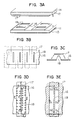
- Figs. 3A to 3E show a liquid crystal display device according to a more concrete embodiment of this invention.
- Fig. 3A is a perspective view of a partial structure of the CSH liquid crystal display device.
- a pair of glass substrate 11 and 12 are disposed to face each other and to define a space for containing the liquid crystal.
- a plurality of common electrode 16 are disposed in parallel.
- elongated apertures 18 are formed substantially perpendicular to the direction in which the common electrode extends.
- a plurality of thinner segment electrodes 17 are disposed in parallel and perpendicular to the direction of the common electrode 12.
- crossed polarizers 13 and 14 are disposed.
- Fig. 3B shows an example of the configuration of the electrode crossing area.
- elongated apertures 18 are formed along the direction perpendicular to the longitudinal direction of the common electrode 16 and corresponding to each central portion of the segment electrode 17.
- the position where the segment electrode 17 are to be disposed are shown in broken lines.
- the segment electrode 17 has a width of about 100 ⁇ m while the common electrode 16 has a width of about 300 ⁇ m.
- the cell gap between the two electrodes is, for example, about 5 ⁇ m.
- the aperture 18 has, for example, a width of about 10 ⁇ m and the length of about 240 ⁇ m.
- the aperture 18 is disposed centrally to the segment electrode 17.
- the segment electrode 17 has a width of about 45 ⁇ m and either side of the aperture 18. Also, there remains a width of about 30 ⁇ m between each longitudinal edge of the aperture 18 and the edge of the common electrode 16.
- the common electrode 16 is formed, for example, of indium tin oxide (ITO) and has a sheet resistance of about 10 ⁇ / ⁇ .
- the width of the aperture 18 is preferably determined relative to the thickness of the liquid crystal layer. For example, when the liquid crystal layer has a thickness of about 5 ⁇ m, the aperture 18 is designed to have a width of not less than about 10 ⁇ m. Then, the electric field can be effectively tilted in the aperture 18.
- Fig. 3C schematically shows the electric field distribution in the electrode crossing area.
- the segment electrode 17 extend perpendicular to the plan of sheet, and the common electrode 16 extend horizontally in the sheet. Due to the existence of the aperture 18, the electric force line emanating from the central portion of the segment electrode 17 can not exist vertically in the figure, and hence is directed to the edge of the aperture 18.
- the electric force line going to the edge of the aperture 18 will be slanted about 45 degrees relative to the normal of the surface of the electrode. The direction of this slant is of the same direction to the fringe electric field at the edge portion of the segment electrode 17.
- the right side part has an electric field which are uniformly slanted in one direction
- the left side part has an electric field which is uniformly slanted in the opposite direction.
- Fig. 3D shows how the liquid crystal molecules are oriented by the electric field thus formed.
- the lateral component of the electric field is represented by arrows.
- a case where the electric field is formed from the common electrode 16 to the segment electrode 17 is shown.
- the electric field enanating from the common electrode 16 and terminating to the segment electrode 17 has a lateral component which are directed form the right side to the left side in the figure.
- the electric field emanating from the common electrode 16 to the segment electrode 17 has a lateral component directed from the left side to the right side. Due to these lateral electric field component, the liquid crystal molecules are slanted in the opposite direction on the right hand side and on the left hand side of the aperture.
- the electrode crossing area where the liquid crystal molecules are oriented in this way appears, for example, as shown Fig. 3E.
- a uniform wide region D1 formed on the left hand side of the aperture 18, a uniform wide region D1 formed, and on the right hand side of the aperture a similarly uniform and wide region D2 is formed.
- narrow regions D3 and D4 are formed on the upper side and the lower side of the aperture 18.
- yet smaller region D4' is formed between the aperture 18 and the region D3.
- similarly yet smaller region D3' is formed between the region D4 and aperture 18.
- the width of the aperture at least twice the thickness of the liquid crystal layer and hence to slant the direction of the electric field at the aperture at least about 45 degrees from the normal to the surface.
- the resistance of the common electrode thereat increases to some extent.
- the width of the aperture and the width of the common electrode remaining at the both sides of the aperture are selected appropriately, for example, so that the sum of the widths of the region of the common electrode remaining on the both sides of the aperture is preferably set at least five times the width of the aperture.
- the liquid crystal display device When the aperture is disposed centrally to the segment electrode, the liquid crystal display device show a symmetric performance with respect to the observation angle. In at least half of the electrode crossing area, display can be rigidly done. Thus, it is prevented to cause a black hole like observation angle where the brightness and the contrast are very low, in the neighborhood of the normal to the surface of the liquid crystal display device.
- the regions D3 and D4 having different orientation directions, formed at the both edges of the aperture can be suppressed in area to be each about 5 % or less of the total display area of the electrode crossing area.
- electric field distribution between the electrodes can be made stable and uniform by providing the aperture in one electrode in the electrode crossing area to improve the quality of display.
Abstract
Description
- This invention relates to a liquid crystal display device, and more particularly to a dot matrix type liquid crystal display device adapted for displaying arbitrary shape on a display surface.
- Although description will mainly be made, taking color super homeotropic (CSH) liquid crystal display (LCD) as an example, the invention is not limited to CSH LCD. For example, it can also be applied to a homogeneous LCD.
- In a CSH LCD, homeotropically or substantially homeotropically oriented nematic liquid crystal molecules are electrically controlled their birefringence to achieve a desired display.
- A CSH LCD without pre-tilt according to the prior art will be described, referring to Figs. 2A to 2D.
- As shown in Fig. 2A, a
liquid crystal molecule 10 has an elongated shape, and has a higher optical constant (refractive index) along the long axis. Further, the liquid crystal molecule has an electric bipole along a direction orthogonal to the long axis. In the "off" state where an electric field above a certain value is not applied between the electrodes, the liquid crystal molecules take a homeotropic orientation where the long axis is normal to the surface of the substrate, as shown in the left part of the figure. When an electric field E is applied normal to the substrate, there occurs a force in a direction which drives the electric dipole of the liquid crystal molecules to follow the direction of the electric field and theliquid crystal molecule 10 is tilted as shown in the right part of the figure. This angle of tilt is called tilt angle, and is of the order of 10 degrees, for example. - Fig. 2B shows an electric field distribution in the electrode crossing portion in the liquid crystal display device. A pair of
glass substrates common electrode 2 are formed in a crossing relation. Thecommon electrode 2 defines the row of the dot matrix and the segment electrodes 1a and 1b define the column of the dot matrix. On the outer surfaces of theglass substrate polarizers common electrode 2, an electric field is established between the electrodes. At the edge of the electrode, fringe effect due to the edge is produced. Namely, the electric force line starting form the edge of the segment electrode 1a or 1b, for example, is bulged towards thecommon electrode 2 as shown by the broken line in the figure to have a lateral or horizontal component as well as the vertical component. The liquid crystal molecule changes its tilt according to the electric field distribution. - Such distribution of the liquid crystal molecules is shown in Fig. 2C in more detail.
- Fig. 2C shows schematically how the liquid crystal molecules are distributed in the
electrode crossing area 5. Theelectrode crossing area 5 is defined between the vertical facingedges 6a and 6b and between the horizontal facingedges 7a and 7b. Since thecommon electrode 2 extends long in the horizontal direction, the electric force line at thefacing edges 6a and 6b, starting from the edges of the segment electrodes 1a and 1b are diverged outwardly as shown by the arrow. Since the segment electrodes 1a and 1b extend long the vertical direction, the electric force line at the horizontal facingedges 7a and 7b of theelectrode crossing area 5, starting from the segment electrode are distributed to be oriented from the outside to the inside. Here, the polarization axes P1 and P2 of the crossed polarizers are disposed at angles
45 degrees slanted from both the row and the column as shown in the right part of the figure. The liquid crystal molecule has a function of rotating the polarized light when tilted from the normal direction, but those liquid crystal molecules which slanted in the direction of the polarization axes P1 and P2 have no such function. Therefore, the light is cut off by the crossed polarizers. - Therefore, as shown in Fig. 2D, there appear crossing black lines in each sell. Namely, as shown in Fig. 2D, the
electrode crossing area 5 is divided into four regions D1, D2, D3 and D4. At the crossing point X of these four regions, the liquid crystal molecules are kept normal to thesubstrates black lines 8, the liquid crystal molecules are tilted in the direction of the polarization axis P1 or P2. In the four regions D1, D2, D3 and D4, the liquid crystal molecules are tilted substantially leftward, rightward, upward and downward, respectively, as shown in Fig. 2D. - In the liquid crystal display device as described above, the shapes and the areas of the four regions D1, D2, D3 and D4 divided by the crossing black lines vary according to the balance of the various condition, are not constant and differ from cell to cell.
- In order to solve the varying and crossing black lines in the display, a preliminary pre-tilt angle in a certain direction may be given to the liquid crystal molecules. For example, referring to Fig. 2D, when a pre-tilt angle of not more than one degree in a direction corresponding to the region D3 is given to the liquid crystal molecules in the whole electrode crossing area, almost all the liquid crystal molecules will be tilted in the same direction when an electric field is applied. Then, the most part of the
electrode crossing area 5 will be occupied by the region D3. Namely, other three regions D1, D2 and D4 become extremely small areas in the display and the quality of display is greatly improved. When such a pre-tilt is given to control the orientation direction of the liquid crystal molecules, another problem arises. - Namely, when the most part of the
electrode crossing area 5 is occupied by the region D3, and when the liquid crystal display device is observed from a direction coinciding the long axes direction of the liquid crystal molecules in the region D3, the liquid crystal molecules lose the optical rotatary power. Then, the whole surface of the display appears black. This black hole like observation angle appears, for example, at a position about 10 degrees from the normal direction to the surface of the liquid crystal display device. The fact that this black hole phenomenon appears very near the normal direction to the surfaces causes a large problem as the performance of the display device. - According to the prior art as described above, the shapes and the positions of the crossing black lines in the display area vary uncertainly to cause a problem in the display performance, or there arises a direction near the normal to the display surface in which the display quality is extremely low.
- An object of this invention is to provide a liquid crystal display device capable of performing display of substantially uniform and good quality in the most part of the electrode crossing area.
- According to an embodiment of this invention, there is provided a dot matrix type liquid crystal display device comprising, a pair of parallel substrates disposed to face each other, two groups of electrodes disposed on said pair of substrates, respectively, and crossing each other when projected normal to one of said substrates, each electrode being elongated and having substantially parallel side edges, at least one elongated aperture formed in one electrode of one of said two groups of electrodes at a portion crossing another electrode of the other group of electrodes along the side edges of said another electrode.
- By providing an elongated aperture in at least one electrode of one of the two groups of electrodes crossing mutually, along the side edges of the crossing electrode, the lateral component of the electric field due to the edge of the electrode crossing area can be positively utilized.
- In the display device which does not utilize the pre-tilt angles, the shape and the areas of the display regions are uncertain. By providing an aperture, the electrode crossing area can be divided almost into two major regions. In each major region, the electric field is tilted in a constant direction to enable uniform display.
- The present invention will be described along the preferred embodiment in conjunction with the accompanying drawings.
- Figs. 1A, 1B and 1C show basic embodiments of this invention. Fig. 1A is a plan view of the first structure. Fig. 1B is a plan view of the second structure. Fig. 1C is a cross section for showing the electric field distribution in the cell schematically
- Figs. 2A, 2B, 2C and 2D show the prior art. Fig. 2A is a schematic cross section showing the liquid crystal molecule. Fig. 2B is a schematic cross section for showing the orientation of the liquid crystal molecules in the electrode crossing area. Fig. 2C is a schematic plan view for illustrating the orientation of the liquid crystal molecules in the "on" states. Fig. 2D is a plan view showing an example of display appearance of the device of Fig. 2C.
- Figs. 3A, 3B, 3C, 3D and 3E show a liquid crystal display device according to more concrete embodiment of this invention. Fig. 3A is a perspective view of the structure. Fig. 3B is a plan view showing the arrangement of the electrode crossing area. Fig. 3C is schematic cross section illustrating the electric field distribution. Fig. 3D is schematic plan view for illustrating the orientation of the liquid crystal molecules. Fig. 3E is a plan view for illustrating an example of the display appearance.
- In the figures, reference numerals denote the followings: 1 electrodes of one group, 2 electrodes of the other group, 3 aperture, 5 electrode crossing area, 10 liquid crystal molecule, 11 and 12 glass substrates, 13 and 14 crossed polarizers, 16 common electrode, 17 segment electrode and 18 aperture.
- Firstly, the basic embodiments of this invention are shown in Figs. 1A to 1C. In a dot matrix type liquid crystal display device, two groups of parallel stripe electrode are formed on a pair of facing transparent substrates respectively, to cross each other. In Figs. 1A to 1C, one
electrode crossing area 5 is shown. - Fig. 1A shows a first embodiment of the electrode. In the figure, an
electrode 1 of one group disposed horizontally and anotherelectrode 2 of another group disposed vertically are disposed to cross orthogonally each other. Although each one electrode is shown in the figure, there are provided a multiplicity of electrodes in each group in a practical dot matrix type liquid crystal display device. In theelectrodes 1 of one group among the crossing two groups of electrodes,apertures 3 are formed substantially parallel to the edges (the edges extending vertically in the figure) of theelectrodes 2 of the other group. Namely, anaperture 3 is formed in eachelectrode crossing area 5 to divide theelectrode crossing area 5 largely into two regions. - Fig. 1B shows a second embodiment of the electrodes. In this structure, instead of providing apertures in the
electrode 1 of the one group,apertures 3 are formed in theelectrodes 2 of the other group, which are disposed substantially parallel to the edges of the electrodes of the one group. The electrode crossing area is divided by theaperture 3 into the upper and lower regions. - By forming the
apertures 3 in theelectrode crossing area 5, the electric field distribution in the electrode crossing area becomes as shown Fig. 1C. Fig. 1C shows the case of Fig. 1A, but when the configuration is turned upside down as indicated by the reference numerals in the parentheses, it shows the case of Fig. 1B. - In Fig. 1C, an
electrode 2 of the other group disposed in the lower part extends perpendicular to the plane of sheet, and anotherelectrode 1 of the one group disposed on the upper side extend horizontally. In theelectrode 1 of one group, anaperture 3 is formed. The electric force line starting from the central portion of theelectrode 2 of the other group toward theelectrode 1 of one group is directed to the edge of theaperture 3, while being diverged. At the edges of theelectrode 2 of the other group, the electric force lines are slanted outwards due to the existence of theelectrode 1 of the one group extending horizontally. Therefore, in the right part of the electrode crossing area, the electric force lines are slanted rightward from the normal direction, and in the left part, the electric force lines are slanted leftward. Namely, theelectrode crossing area 5 is divided into substantially uniform two regions by the aperture. The division is almost uniquely determined by the position of the aperture. Thus, uniform display can be obtained throughout the liquid crystal display device. Further, when the liquid crystal display device is observed while being slanted in the state where an electric field is applied, even when half of the electrode crossing area appears black when the liquid crystal display device is observed from the direction of the arrow shown in the right part of the figure, the remaining half of the display surface keeps the normal display. Thus, the phenomenon that the liquid crystal display surface becomes totally black as appears in the conventional liquid crystal display device utilizing the pre-tilt can be prevented. - Figs. 3A to 3E show a liquid crystal display device according to a more concrete embodiment of this invention.
- Fig. 3A is a perspective view of a partial structure of the CSH liquid crystal display device. A pair of
glass substrate lower glass substrate 11, a plurality ofcommon electrode 16 are disposed in parallel. In thecommon electrode 16,elongated apertures 18 are formed substantially perpendicular to the direction in which the common electrode extends. On the surface of theupper glass substrate 12, a plurality ofthinner segment electrodes 17 are disposed in parallel and perpendicular to the direction of thecommon electrode 12. On the outside of thepair glass substrates polarizers - Fig. 3B shows an example of the configuration of the electrode crossing area. In the
common electrode 16,elongated apertures 18 are formed along the direction perpendicular to the longitudinal direction of thecommon electrode 16 and corresponding to each central portion of thesegment electrode 17. The position where thesegment electrode 17 are to be disposed are shown in broken lines. For example, thesegment electrode 17 has a width of about 100 µm while thecommon electrode 16 has a width of about 300 µm. The cell gap between the two electrodes is, for example, about 5 µm. Theaperture 18 has, for example, a width of about 10 µm and the length of about 240 µm. Theaperture 18 is disposed centrally to thesegment electrode 17. Therefor, thesegment electrode 17 has a width of about 45 µm and either side of theaperture 18. Also, there remains a width of about 30 µm between each longitudinal edge of theaperture 18 and the edge of thecommon electrode 16. - The
common electrode 16 is formed, for example, of indium tin oxide (ITO) and has a sheet resistance of about 10 Ω/□ . The width of theaperture 18 is preferably determined relative to the thickness of the liquid crystal layer. For example, when the liquid crystal layer has a thickness of about 5 µm, theaperture 18 is designed to have a width of not less than about 10 µm. Then, the electric field can be effectively tilted in theaperture 18. - Fig. 3C schematically shows the electric field distribution in the electrode crossing area. The
segment electrode 17 extend perpendicular to the plan of sheet, and thecommon electrode 16 extend horizontally in the sheet. Due to the existence of theaperture 18, the electric force line emanating from the central portion of thesegment electrode 17 can not exist vertically in the figure, and hence is directed to the edge of theaperture 18. In the case when the liquid crystal layer has a thickness of about 5 µm and theaperture 18 has a width of about 10 µm, the electric force line going to the edge of theaperture 18 will be slanted about 45 degrees relative to the normal of the surface of the electrode. The direction of this slant is of the same direction to the fringe electric field at the edge portion of thesegment electrode 17. Thus, forming a boundary at theaperture 18, the right side part has an electric field which are uniformly slanted in one direction, and the left side part has an electric field which is uniformly slanted in the opposite direction. - Fig. 3D shows how the liquid crystal molecules are oriented by the electric field thus formed. In the figure, the lateral component of the electric field is represented by arrows. A case where the electric field is formed from the
common electrode 16 to thesegment electrode 17 is shown. On the righthand side of theaperture 18, the electric field enanating from thecommon electrode 16 and terminating to thesegment electrode 17 has a lateral component which are directed form the right side to the left side in the figure. In the left hand side of theaperture 18, the electric field emanating from thecommon electrode 16 to thesegment electrode 17 has a lateral component directed from the left side to the right side. Due to these lateral electric field component, the liquid crystal molecules are slanted in the opposite direction on the right hand side and on the left hand side of the aperture. Here, between the edges of theaperture 18 and the edges of thecommon electrode 16, there are produced other regions where the liquid crystal molecules are oriented in other directions. - The electrode crossing area where the liquid crystal molecules are oriented in this way appears, for example, as shown Fig. 3E. Namely, on the left hand side of the
aperture 18, a uniform wide region D1 formed, and on the right hand side of the aperture a similarly uniform and wide region D2 is formed. On the upper side and the lower side of theaperture 18, narrow regions D3 and D4 are formed. Further, in the upper area, yet smaller region D4' is formed between theaperture 18 and the region D3. Also, in the lower side of theaperture 18 similarly yet smaller region D3' is formed between the region D4 andaperture 18. These small regions D3 and D4 and yet smaller region D3' and D4' only occupy very small area in the display area. Therefor, even when the shapes and the positions of these regions may vary to some extent, the influence thereof to the display quality is low. - It is preferable, as described above, to have the width of the aperture at least twice the thickness of the liquid crystal layer and hence to slant the direction of the electric field at the aperture at least about 45 degrees from the normal to the surface. Here, by forming the aperture in the common electrode, the resistance of the common electrode thereat increases to some extent. For depressing the increase of the resistance not to give substantial obstacle, the width of the aperture and the width of the common electrode remaining at the both sides of the aperture are selected appropriately, for example, so that the sum of the widths of the region of the common electrode remaining on the both sides of the aperture is preferably set at least five times the width of the aperture.
- When the aperture is disposed centrally to the segment electrode, the liquid crystal display device show a symmetric performance with respect to the observation angle. In at least half of the electrode crossing area, display can be rigidly done. Thus, it is prevented to cause a black hole like observation angle where the brightness and the contrast are very low, in the neighborhood of the normal to the surface of the liquid crystal display device.
- The regions D3 and D4 having different orientation directions, formed at the both edges of the aperture can be suppressed in area to be each about 5 % or less of the total display area of the electrode crossing area.
- In this way, uniform CSH liquid crystal display device without a black hole where the brightness and the contrast decreases extremely, can be produced.
- As is described above, according to the embodiments of this invention, electric field distribution between the electrodes can be made stable and uniform by providing the aperture in one electrode in the electrode crossing area to improve the quality of display.
- Although the description has been made on preferred embodiments of this invention, the present invention is not limited thereto. For example, it will be apparent to those skilled in the art that various substitutions, alterations, replacements, improvements or combinations are possible within the scope of the claims.
Claims (6)
- A dot matrix type liquid crystal display device comprising:
a pair of parallel substrates disposed to face each other;
two groups of electrodes disposed on said pair of substrates, respectively, and crossing each other when projected normal to one of said substrates, each electrode being elongated and having substantially parallel side edges;
at least one elongated aperture formed in one electrode of one of said two groups of electrodes at a portion crossing another electrode of the other group of electrodes along the side edges of said another electrode. - A dot matrix type liquid crystal display device according to claim 1, wherein said one electrode of one of said two groups of electrodes has a larger width than said another electrode of the other group of electrodes.
- A dot matrix type liquid crystal display device according to claim 1, wherein said elongated aperture is disposed at a portion in a width of said another electrode of the other group of electrodes, when projected normal to one of said substrates.
- A dot matrix type liquid crystal display device according to claim 3, wherein said elongated aperture is disposed at a central portion in a width of said another electrode of the other group of electrodes, when projected normal to one of said substrates.
- A dot matrix type liquid crystal display device according to claim 3, wherein said two groups of electrodes has a gap therebetween at the crossing portion and said elongated aperture has a first width in a lateral direction thereof which is at least about twice the gap between the electrodes.
- A dot matrix type liquid crystal display device according to claim 4, wherein said elongated aperture has a first width in a lateral direction thereof and define said portions in said one electrode adjacent to the elongated aperture, and the side portion has a second width in a longitudinal direction of the elongated aperture, which is at least about fifth times of the first width.
Applications Claiming Priority (2)
| Application Number | Priority Date | Filing Date | Title |
|---|---|---|---|
| JP2057783A JP2507122B2 (en) | 1990-03-08 | 1990-03-08 | Liquid crystal display |
| JP57783/90 | 1990-03-08 |
Publications (3)
| Publication Number | Publication Date |
|---|---|
| EP0445777A2 true EP0445777A2 (en) | 1991-09-11 |
| EP0445777A3 EP0445777A3 (en) | 1992-05-20 |
| EP0445777B1 EP0445777B1 (en) | 1995-11-22 |
Family
ID=13065476
Family Applications (1)
| Application Number | Title | Priority Date | Filing Date |
|---|---|---|---|
| EP91103419A Expired - Lifetime EP0445777B1 (en) | 1990-03-08 | 1991-03-06 | Liquid crystal display device |
Country Status (4)
| Country | Link |
|---|---|
| US (1) | US5136407A (en) |
| EP (1) | EP0445777B1 (en) |
| JP (1) | JP2507122B2 (en) |
| DE (1) | DE69114736T2 (en) |
Cited By (10)
| Publication number | Priority date | Publication date | Assignee | Title |
|---|---|---|---|---|
| EP0534467A1 (en) * | 1991-09-26 | 1993-03-31 | Kabushiki Kaisha Toshiba | Improvement in electrode structure of liquid crystal display device and method of manufacturing the liquid crystal display device |
| US5309264A (en) * | 1992-04-30 | 1994-05-03 | International Business Machines Corporation | Liquid crystal displays having multi-domain cells |
| EP0636921A2 (en) * | 1993-07-27 | 1995-02-01 | Kabushiki Kaisha Toshiba | Liquid crystal device |
| EP0636917A1 (en) * | 1993-07-27 | 1995-02-01 | Sharp Kabushiki Kaisha | Liquid crystal display |
| EP0731374A1 (en) * | 1995-03-09 | 1996-09-11 | THOMSON multimedia | Liquid crystal display with improved viewing angle |
| EP0793134A1 (en) * | 1996-02-27 | 1997-09-03 | Stanley Electric Co., Ltd. | Liquid crystal display having alternating cuts in electrodes |
| US6661488B1 (en) | 1997-06-12 | 2003-12-09 | Fujitsu Limited | Vertically-alligned (VA) liquid crystal display device |
| US7570332B2 (en) | 1998-05-16 | 2009-08-04 | Samsung Electronics Co., Ltd. | Liquid crystal displays having multi-domains and a manufacturing method thereof |
| US7583345B2 (en) | 1999-10-01 | 2009-09-01 | Samsung Electronics Co., Ltd. | Liquid crystal display |
| US7768615B2 (en) | 1997-05-29 | 2010-08-03 | Samsung Electronics Co., Ltd. | Liquid crystal display having wide viewing angle |
Families Citing this family (30)
| Publication number | Priority date | Publication date | Assignee | Title |
|---|---|---|---|---|
| JPH0412326A (en) * | 1990-05-01 | 1992-01-16 | Canon Inc | Liquid crystal element |
| JPH0786622B2 (en) * | 1990-11-02 | 1995-09-20 | スタンレー電気株式会社 | Liquid crystal display |
| GB2255193B (en) * | 1991-04-24 | 1994-10-12 | Marconi Gec Ltd | Optical device |
| JPH06301036A (en) * | 1993-04-12 | 1994-10-28 | Sanyo Electric Co Ltd | Liquid crystal display device |
| JP2693368B2 (en) * | 1993-06-29 | 1997-12-24 | スタンレー電気株式会社 | Liquid crystal display device and method of manufacturing the same |
| JPH0961825A (en) * | 1995-08-28 | 1997-03-07 | Sharp Corp | Liquid crystal display device |
| US6157428A (en) * | 1997-05-07 | 2000-12-05 | Sanyo Electric Co., Ltd. | Liquid crystal display |
| US6465268B2 (en) * | 1997-05-22 | 2002-10-15 | Semiconductor Energy Laboratory Co., Ltd. | Method of manufacturing an electro-optical device |
| KR100286762B1 (en) * | 1997-06-27 | 2001-04-16 | 박종섭 | Liquid crystal display |
| JP3398025B2 (en) | 1997-10-01 | 2003-04-21 | 三洋電機株式会社 | Liquid crystal display |
| JPH11109391A (en) * | 1997-10-01 | 1999-04-23 | Sanyo Electric Co Ltd | Liquid crystal display device |
| JP3008928B2 (en) * | 1998-05-07 | 2000-02-14 | 日本電気株式会社 | Liquid crystal display |
| KR100354904B1 (en) * | 1998-05-19 | 2002-12-26 | 삼성전자 주식회사 | Liquid crystal display with wide viewing angle |
| US6515729B1 (en) * | 1998-07-29 | 2003-02-04 | Citizen Watch Co., Ltd. | Reflection-type color liquid crystal display device |
| KR100312753B1 (en) | 1998-10-13 | 2002-04-06 | 윤종용 | Wide viewing angle liquid crystal display device |
| EP1028346A3 (en) | 1999-02-12 | 2002-05-02 | Matsushita Electric Industrial Co., Ltd. | Liquid crystal element and manufacturing method thereof |
| JP2000275646A (en) | 1999-03-24 | 2000-10-06 | Nec Corp | Liquid crystal display device |
| US6400440B1 (en) * | 1999-06-23 | 2002-06-04 | International Business Machines Corporation | Passive liquid crystal display having pre-tilt control structure and light absorbent material at a center |
| US6778229B2 (en) * | 2001-10-02 | 2004-08-17 | Fujitsu Display Technologies Corporation | Liquid crystal display device and method of fabricating the same |
| JP4197404B2 (en) * | 2001-10-02 | 2008-12-17 | シャープ株式会社 | Liquid crystal display device and manufacturing method thereof |
| US6985202B2 (en) | 2002-05-24 | 2006-01-10 | Hannstar Display Corporation | Biased bending vertical alignment liquid crystal display |
| US6803981B2 (en) * | 2002-05-24 | 2004-10-12 | Hannstar Display Corporation | Liquid crystal display having biased bending vertical alignment |
| US6965423B2 (en) * | 2003-05-13 | 2005-11-15 | Toppoly Optoelectronics Corp. | Liquid crystal display and fabricating method thereof |
| JP2005062724A (en) * | 2003-08-20 | 2005-03-10 | Toshiba Matsushita Display Technology Co Ltd | Optical phase difference plate and liquid crystal display |
| JP4948871B2 (en) * | 2006-03-29 | 2012-06-06 | スタンレー電気株式会社 | Liquid crystal display element |
| KR100922803B1 (en) * | 2006-11-29 | 2009-10-21 | 엘지디스플레이 주식회사 | A liquid crystal display device |
| JP5324754B2 (en) | 2007-05-10 | 2013-10-23 | スタンレー電気株式会社 | Liquid crystal display |
| US20130220672A1 (en) * | 2012-02-28 | 2013-08-29 | Touch Turns, Llc | Single Layer Touch-Control Sensor Structure With Reduced Coupling To Proximate Ground Structures |
| JP6030413B2 (en) * | 2012-11-09 | 2016-11-24 | スタンレー電気株式会社 | Liquid crystal display |
| KR102437424B1 (en) * | 2016-03-15 | 2022-08-30 | 가부시키가이샤 한도오따이 에네루기 켄큐쇼 | Display device, module, and electronic device |
Citations (2)
| Publication number | Priority date | Publication date | Assignee | Title |
|---|---|---|---|---|
| GB2177533A (en) * | 1985-06-18 | 1987-01-21 | Citizen Watch Co Ltd | Electrode structure of liquid-crystal cell |
| JPS62299944A (en) * | 1986-06-20 | 1987-12-26 | Sharp Corp | Liquid crystal light quantity modulation element |
Family Cites Families (7)
| Publication number | Priority date | Publication date | Assignee | Title |
|---|---|---|---|---|
| JPS556233B2 (en) * | 1974-08-07 | 1980-02-14 | ||
| JPS5820433B2 (en) * | 1975-10-23 | 1983-04-22 | 株式会社日立製作所 | EXIYO HIYOJISOSHI |
| JPS6046225A (en) * | 1983-08-25 | 1985-03-13 | Sumitomo Chem Co Ltd | Preparation of aromatic polyester film |
| YU44866B (en) * | 1983-09-09 | 1991-04-30 | Inst Stefan Jozef | Matrix lcd with an internal reflector and a measuring net |
| FR2596187B1 (en) * | 1986-03-18 | 1988-05-13 | Commissariat Energie Atomique | METHOD FOR SEQUENTIALLY CONTROLLING A LIQUID CRYSTAL MATRIX DISPLAY HAVING DIFFERENT OPTICAL RESPONSES IN ALTERNATIVE AND CONTINUOUS FIELDS |
| FR2598827B1 (en) * | 1986-05-14 | 1992-10-02 | Centre Nat Rech Scient | IMPROVEMENTS ON LIQUID CRYSTAL OPTICAL DEVICES, ALLOWING THE IMPLEMENTATION OF HIGH FREQUENCY ALTERNATIVE EXCITATIONS. |
| GB2212659A (en) * | 1987-11-20 | 1989-07-26 | Philips Electronic Associated | Multi-level circuit cross-overs |
-
1990
- 1990-03-08 JP JP2057783A patent/JP2507122B2/en not_active Expired - Lifetime
-
1991
- 1991-03-04 US US07/664,035 patent/US5136407A/en not_active Expired - Lifetime
- 1991-03-06 DE DE69114736T patent/DE69114736T2/en not_active Expired - Lifetime
- 1991-03-06 EP EP91103419A patent/EP0445777B1/en not_active Expired - Lifetime
Patent Citations (2)
| Publication number | Priority date | Publication date | Assignee | Title |
|---|---|---|---|---|
| GB2177533A (en) * | 1985-06-18 | 1987-01-21 | Citizen Watch Co Ltd | Electrode structure of liquid-crystal cell |
| JPS62299944A (en) * | 1986-06-20 | 1987-12-26 | Sharp Corp | Liquid crystal light quantity modulation element |
Non-Patent Citations (2)
| Title |
|---|
| JAPANESE JOURNAL OF APPLIED PHYSICS. vol. 20, no. 11, November 1981, TOKYO JP pages 2025 - 2031; T.UMEDA ET AL.: 'Method of Evaluating Tilt Domain in a Twisted Nematic Cell' * |
| PATENT ABSTRACTS OF JAPAN vol. 12, no. 194 (P-713)(3041) 7 June 1988 & JP-A-62 299 944 ( SHARP ) * |
Cited By (36)
| Publication number | Priority date | Publication date | Assignee | Title |
|---|---|---|---|---|
| US5646705A (en) * | 1991-09-26 | 1997-07-08 | Kabushiki Kaisha Toshiba | Electrode structure of liquid crystal display device and method of manufacturing the liquid crystal display device |
| EP0534467A1 (en) * | 1991-09-26 | 1993-03-31 | Kabushiki Kaisha Toshiba | Improvement in electrode structure of liquid crystal display device and method of manufacturing the liquid crystal display device |
| US5309264A (en) * | 1992-04-30 | 1994-05-03 | International Business Machines Corporation | Liquid crystal displays having multi-domain cells |
| US5953093A (en) * | 1993-07-17 | 1999-09-14 | Sharp Kabushiki Kaisha | Liquid crystal display having two or more spacings between electrodes |
| US6141077A (en) * | 1993-07-27 | 2000-10-31 | Sharp Kabushiki Kaisha | Liquid crystal display including pixel electrode(s) designed to improve viewing characteristics |
| EP0636921A3 (en) * | 1993-07-27 | 1995-07-05 | Tokyo Shibaura Electric Co | Liquid crystal device. |
| US5872611A (en) * | 1993-07-27 | 1999-02-16 | Sharp Kabushiki Kaisha | Liquid crystal display having two or more spacings between electrodes |
| EP0636917A1 (en) * | 1993-07-27 | 1995-02-01 | Sharp Kabushiki Kaisha | Liquid crystal display |
| EP0636921A2 (en) * | 1993-07-27 | 1995-02-01 | Kabushiki Kaisha Toshiba | Liquid crystal device |
| US6342939B1 (en) | 1993-07-27 | 2002-01-29 | Sharp Kabushiki Kaisha | Liquid crystal display including pixel electrode (S) designed to improve viewing characteristics |
| EP0731374A1 (en) * | 1995-03-09 | 1996-09-11 | THOMSON multimedia | Liquid crystal display with improved viewing angle |
| FR2731526A1 (en) * | 1995-03-09 | 1996-09-13 | Thomson Consumer Electronics | LIQUID CRYSTAL SCREEN WITH IMPROVED ANGLE OF VIEW |
| US6327014B1 (en) | 1995-03-09 | 2001-12-04 | Thomson Licensing S.A. | Liquid crystal screen with enlarged viewing angle |
| EP0793134A1 (en) * | 1996-02-27 | 1997-09-03 | Stanley Electric Co., Ltd. | Liquid crystal display having alternating cuts in electrodes |
| US5777711A (en) * | 1996-02-27 | 1998-07-07 | Stanley Electric Co., Ltd. | Liquid crystal display having balanced cuts in electrodes |
| US9041891B2 (en) | 1997-05-29 | 2015-05-26 | Samsung Display Co., Ltd. | Liquid crystal display having wide viewing angle |
| US7768615B2 (en) | 1997-05-29 | 2010-08-03 | Samsung Electronics Co., Ltd. | Liquid crystal display having wide viewing angle |
| US7224421B1 (en) | 1997-06-12 | 2007-05-29 | Sharp Kabushiki Kaisha | Vertically-aligned (VA) liquid crystal display device |
| US8134671B2 (en) | 1997-06-12 | 2012-03-13 | Sharp Kabushiki Kaisha | Liquid crystal display device |
| US7227606B2 (en) | 1997-06-12 | 2007-06-05 | Sharp Kabushiki Kaisha | Vertically-alligned (VA) liquid crystal display device |
| US7304703B1 (en) | 1997-06-12 | 2007-12-04 | Sharp Kabushiki Kaisha | Vertically-aligned (VA) liquid crystal display device |
| US6661488B1 (en) | 1997-06-12 | 2003-12-09 | Fujitsu Limited | Vertically-alligned (VA) liquid crystal display device |
| US7167224B1 (en) | 1997-06-12 | 2007-01-23 | Sharp Kabushiki Kaisha | Vertically-aligned (VA) liquid crystal display device |
| US8553188B2 (en) | 1997-06-12 | 2013-10-08 | Sharp Kabushiki Kaisha | Liquid crystal display device |
| US7760305B2 (en) | 1997-06-12 | 2010-07-20 | Sharp Kabushiki Kaisha | Liquid crystal display device with multiple alignment structures |
| US6724452B1 (en) | 1997-06-12 | 2004-04-20 | Fujitsu Display Technologies Corporation | Vertically aligned (VA) liquid crystal display device |
| US7821603B2 (en) | 1997-06-12 | 2010-10-26 | Sharp Kabushiki Kaisha | Vertically-alligned (VA) liquid crystal display device |
| US7965363B2 (en) | 1997-06-12 | 2011-06-21 | Sharp Kabushiki Kaisha | Vertically-aligned (VA) liquid crystal display device |
| USRE43123E1 (en) | 1997-06-12 | 2012-01-24 | Sharp Kabushiki Kaisha | Vertically-aligned (VA) liquid crystal display device |
| US7573554B2 (en) | 1998-05-16 | 2009-08-11 | Samsung Electronics Co., Ltd. | Liquid crystal displays having multi-domains and a manufacturing method thereof |
| US7570332B2 (en) | 1998-05-16 | 2009-08-04 | Samsung Electronics Co., Ltd. | Liquid crystal displays having multi-domains and a manufacturing method thereof |
| US8174651B2 (en) | 1999-10-01 | 2012-05-08 | Samsung Electronics Co., Ltd. | Liquid crystal display |
| US8456597B2 (en) | 1999-10-01 | 2013-06-04 | Samsung Display Co., Ltd. | Liquid crystal display |
| US7583345B2 (en) | 1999-10-01 | 2009-09-01 | Samsung Electronics Co., Ltd. | Liquid crystal display |
| US8817213B2 (en) | 1999-10-01 | 2014-08-26 | Samsung Display Co., Ltd. | Liquid crystal display |
| US9557612B2 (en) | 1999-10-01 | 2017-01-31 | Samsung Display Co., Ltd. | Liquid crystal display |
Also Published As
| Publication number | Publication date |
|---|---|
| EP0445777B1 (en) | 1995-11-22 |
| US5136407A (en) | 1992-08-04 |
| EP0445777A3 (en) | 1992-05-20 |
| JPH03259121A (en) | 1991-11-19 |
| DE69114736T2 (en) | 1996-09-05 |
| DE69114736D1 (en) | 1996-01-04 |
| JP2507122B2 (en) | 1996-06-12 |
Similar Documents
| Publication | Publication Date | Title |
|---|---|---|
| US5136407A (en) | Liquid crystal display having apertures in the electrodes | |
| US5229873A (en) | Liquid crystal display having apertures in both electrodes | |
| US7619708B2 (en) | Multi-domain liquid crystal display device | |
| JP2565639B2 (en) | Liquid crystal display | |
| KR100248210B1 (en) | Liquid crystal display device | |
| KR100482468B1 (en) | Fringe field switching mode lcd | |
| US8054430B2 (en) | Liquid crystal display having wide viewing angle | |
| US6704083B1 (en) | Liquid crystal display including polarizing plate having polarizing directions neither parallel nor perpendicular to average alignment direction of molecules | |
| EP0793134B1 (en) | Liquid crystal display having alternating cuts in electrodes | |
| US6950169B2 (en) | Vertical alignment mode liquid crystal display device having pixel electrode partially covering holes of the insulating film | |
| US20030202144A1 (en) | Liquid crystal display having wide viewing angle | |
| JP5096857B2 (en) | Liquid crystal display element | |
| JPH08101399A (en) | Liquid crystal display device | |
| JPH0736044A (en) | Pixel orientation dividing type liquid crystal display element | |
| KR100492325B1 (en) | In plane switching mode liquid crystal display device | |
| US20060087607A1 (en) | Multi-domain vertical alignment liquid crystal display device | |
| KR100601173B1 (en) | a liquid crystal display | |
| CN111812895A (en) | Pixel electrode and liquid crystal display panel | |
| KR100306806B1 (en) | Liquid crystal display | |
| JP3231910B2 (en) | Liquid crystal display device | |
| KR100737571B1 (en) | LCD device having wide viewing angle | |
| JPH07294934A (en) | Liquid crystal device | |
| KR20020044283A (en) | Fringe field swiching mode lcd | |
| US20020075213A1 (en) | Liquid crystal display device | |
| KR20010110089A (en) | Fringe field swiching mode lcd |
Legal Events
| Date | Code | Title | Description |
|---|---|---|---|
| PUAI | Public reference made under article 153(3) epc to a published international application that has entered the european phase |
Free format text: ORIGINAL CODE: 0009012 |
|
| AK | Designated contracting states |
Kind code of ref document: A2 Designated state(s): DE FR GB IT NL |
|
| PUAL | Search report despatched |
Free format text: ORIGINAL CODE: 0009013 |
|
| AK | Designated contracting states |
Kind code of ref document: A3 Designated state(s): DE FR GB IT NL |
|
| 17P | Request for examination filed |
Effective date: 19921113 |
|
| 17Q | First examination report despatched |
Effective date: 19940628 |
|
| GRAA | (expected) grant |
Free format text: ORIGINAL CODE: 0009210 |
|
| AK | Designated contracting states |
Kind code of ref document: B1 Designated state(s): DE FR GB IT NL |
|
| PG25 | Lapsed in a contracting state [announced via postgrant information from national office to epo] |
Ref country code: IT Free format text: LAPSE BECAUSE OF FAILURE TO SUBMIT A TRANSLATION OF THE DESCRIPTION OR TO PAY THE FEE WITHIN THE PRESCRIBED TIME-LIMIT;WARNING: LAPSES OF ITALIAN PATENTS WITH EFFECTIVE DATE BEFORE 2007 MAY HAVE OCCURRED AT ANY TIME BEFORE 2007. THE CORRECT EFFECTIVE DATE MAY BE DIFFERENT FROM THE ONE RECORDED. Effective date: 19951122 Ref country code: NL Free format text: LAPSE BECAUSE OF FAILURE TO SUBMIT A TRANSLATION OF THE DESCRIPTION OR TO PAY THE FEE WITHIN THE PRESCRIBED TIME-LIMIT Effective date: 19951122 |
|
| REF | Corresponds to: |
Ref document number: 69114736 Country of ref document: DE Date of ref document: 19960104 |
|
| ET | Fr: translation filed | ||
| NLV1 | Nl: lapsed or annulled due to failure to fulfill the requirements of art. 29p and 29m of the patents act | ||
| PLBE | No opposition filed within time limit |
Free format text: ORIGINAL CODE: 0009261 |
|
| STAA | Information on the status of an ep patent application or granted ep patent |
Free format text: STATUS: NO OPPOSITION FILED WITHIN TIME LIMIT |
|
| 26N | No opposition filed | ||
| REG | Reference to a national code |
Ref country code: GB Ref legal event code: IF02 |
|
| REG | Reference to a national code |
Ref country code: GB Ref legal event code: 732E |
|
| REG | Reference to a national code |
Ref country code: FR Ref legal event code: TQ |
|
| PGFP | Annual fee paid to national office [announced via postgrant information from national office to epo] |
Ref country code: FR Payment date: 20100402 Year of fee payment: 20 |
|
| PGFP | Annual fee paid to national office [announced via postgrant information from national office to epo] |
Ref country code: GB Payment date: 20100317 Year of fee payment: 20 |
|
| PGFP | Annual fee paid to national office [announced via postgrant information from national office to epo] |
Ref country code: DE Payment date: 20100330 Year of fee payment: 20 |
|
| REG | Reference to a national code |
Ref country code: DE Ref legal event code: R071 Ref document number: 69114736 Country of ref document: DE |
|
| REG | Reference to a national code |
Ref country code: GB Ref legal event code: PE20 Expiry date: 20110305 |
|
| PG25 | Lapsed in a contracting state [announced via postgrant information from national office to epo] |
Ref country code: GB Free format text: LAPSE BECAUSE OF EXPIRATION OF PROTECTION Effective date: 20110305 |
|
| PG25 | Lapsed in a contracting state [announced via postgrant information from national office to epo] |
Ref country code: DE Free format text: LAPSE BECAUSE OF EXPIRATION OF PROTECTION Effective date: 20110306 |