EP0444943A1 - A method of manufacturing a bonded wafer - Google Patents
A method of manufacturing a bonded wafer Download PDFInfo
- Publication number
- EP0444943A1 EP0444943A1 EP91301680A EP91301680A EP0444943A1 EP 0444943 A1 EP0444943 A1 EP 0444943A1 EP 91301680 A EP91301680 A EP 91301680A EP 91301680 A EP91301680 A EP 91301680A EP 0444943 A1 EP0444943 A1 EP 0444943A1
- Authority
- EP
- European Patent Office
- Prior art keywords
- wafer
- wafers
- face
- oxide film
- bonded
- Prior art date
- Legal status (The legal status is an assumption and is not a legal conclusion. Google has not performed a legal analysis and makes no representation as to the accuracy of the status listed.)
- Granted
Links
Images


Classifications
-
- H—ELECTRICITY
- H01—ELECTRIC ELEMENTS
- H01L—SEMICONDUCTOR DEVICES NOT COVERED BY CLASS H10
- H01L21/00—Processes or apparatus adapted for the manufacture or treatment of semiconductor or solid state devices or of parts thereof
- H01L21/02—Manufacture or treatment of semiconductor devices or of parts thereof
- H01L21/04—Manufacture or treatment of semiconductor devices or of parts thereof the devices having at least one potential-jump barrier or surface barrier, e.g. PN junction, depletion layer or carrier concentration layer
- H01L21/18—Manufacture or treatment of semiconductor devices or of parts thereof the devices having at least one potential-jump barrier or surface barrier, e.g. PN junction, depletion layer or carrier concentration layer the devices having semiconductor bodies comprising elements of Group IV of the Periodic System or AIIIBV compounds with or without impurities, e.g. doping materials
- H01L21/20—Deposition of semiconductor materials on a substrate, e.g. epitaxial growth solid phase epitaxy
- H01L21/2003—Deposition of semiconductor materials on a substrate, e.g. epitaxial growth solid phase epitaxy characterised by the substrate
- H01L21/2007—Bonding of semiconductor wafers to insulating substrates or to semiconducting substrates using an intermediate insulating layer
-
- H—ELECTRICITY
- H01—ELECTRIC ELEMENTS
- H01L—SEMICONDUCTOR DEVICES NOT COVERED BY CLASS H10
- H01L21/00—Processes or apparatus adapted for the manufacture or treatment of semiconductor or solid state devices or of parts thereof
- H01L21/02—Manufacture or treatment of semiconductor devices or of parts thereof
- H01L21/04—Manufacture or treatment of semiconductor devices or of parts thereof the devices having at least one potential-jump barrier or surface barrier, e.g. PN junction, depletion layer or carrier concentration layer
- H01L21/18—Manufacture or treatment of semiconductor devices or of parts thereof the devices having at least one potential-jump barrier or surface barrier, e.g. PN junction, depletion layer or carrier concentration layer the devices having semiconductor bodies comprising elements of Group IV of the Periodic System or AIIIBV compounds with or without impurities, e.g. doping materials
- H01L21/30—Treatment of semiconductor bodies using processes or apparatus not provided for in groups H01L21/20 - H01L21/26
- H01L21/302—Treatment of semiconductor bodies using processes or apparatus not provided for in groups H01L21/20 - H01L21/26 to change their surface-physical characteristics or shape, e.g. etching, polishing, cutting
- H01L21/304—Mechanical treatment, e.g. grinding, polishing, cutting
-
- H—ELECTRICITY
- H01—ELECTRIC ELEMENTS
- H01L—SEMICONDUCTOR DEVICES NOT COVERED BY CLASS H10
- H01L21/00—Processes or apparatus adapted for the manufacture or treatment of semiconductor or solid state devices or of parts thereof
- H01L21/70—Manufacture or treatment of devices consisting of a plurality of solid state components formed in or on a common substrate or of parts thereof; Manufacture of integrated circuit devices or of parts thereof
- H01L21/71—Manufacture of specific parts of devices defined in group H01L21/70
- H01L21/76—Making of isolation regions between components
- H01L21/762—Dielectric regions, e.g. EPIC dielectric isolation, LOCOS; Trench refilling techniques, SOI technology, use of channel stoppers
- H01L21/7624—Dielectric regions, e.g. EPIC dielectric isolation, LOCOS; Trench refilling techniques, SOI technology, use of channel stoppers using semiconductor on insulator [SOI] technology
- H01L21/76251—Dielectric regions, e.g. EPIC dielectric isolation, LOCOS; Trench refilling techniques, SOI technology, use of channel stoppers using semiconductor on insulator [SOI] technology using bonding techniques
Definitions
- This invention relates to a method of manufacturing a bonded wafer, especially a warpless bonded wafer having a high degree of flatness.
- Another conventional technology of providing a single crystal film on a dielectric substrate is characterized by first forming a thermally oxidized oxide film across the surface of the silicon substrate, laying a polycrystal or amorphous silicon film over this oxide film, and applying to this an energy beam such as an electron beam or a laser beam in a manner such that the beam spot thereon is shifted along lines all in one and the same direction to thereby melt the silicon film, and then cooling and solidifying the film to obtain a monolithic single crystal film.
- an energy beam such as an electron beam or a laser beam
- SOI structure Si-on-insulation structure
- Fig. 3 shows an example of the procedure of manufacturing such silicon bonded wafer.
- two semiconductor mirror wafers of silicon single crystal are prepared.
- the one (hereinafter referred to as "the bond wafer") 101 whose upper face, as viewed in Fig. 3, is to be made into the device formation face is subjected to a thermal oxidation treatment whereby a thin oxide film 103 of silicon dioxide is formed throughout the entire surface, or on both main surfaces, of the bond wafer 101.
- the other mirror wafer 102 shall be referred to as "the base wafer", and is employed mainly for a protective purpose, that is, for securing mechanical strength of the final bonded wafer.
- the two wafers 101 and 102 are put together, as shown in Fig. 3, and heated to a predetermined temperature, 500°C for example, to thereby bind them eternally.
- a predetermined temperature 500°C for example
- the upper face of the bond wafer 101 is ground until the thickness of the bond wafer 101 becomes several ⁇ m (the hatched portion of the bond wafer 101 is ground off).
- a bonded wafer 105 is obtained, as shown at (d) of Fig. 3.
- the intermediate silicon dioxide layer is fixed between the two wafers 101, 102 at high temperature, as shown at (b) of Fig. 3.
- residual stress tensile stress mainly
- the coefficient of thermal expansion or the coefficient of thermal contraction of silicon single crystal is greater than that of silicon dioxide.
- the residual stress contained in the bond wafer 101 is mostly relieved and becomes negligible compared with that in the base wafer 102, and as a result, the residual stress in the base wafer 102, especially that accumulated near the oxide film 103, causes the bonded wafer 105 to warp as shown at (d) of Fig. 3.
- the base wafer 102 without the oxide film 103 shrinks greater than the bond wafer 101.
- the bonded wafer 105 arches in a manner such that the side of the bond wafer 101 forms the convex, and the magnitude of warpage is generally 100 - 200 ⁇ m.
- the bonded wafer 105 is warped, as shown at (d) of Fig. 3, problems are experienced when the bonded wafer 105 has to be attached to the level block of a grinder by suction or with wax for further grinding of the bond wafer 101, because it is difficult to hold the warped wafer onto the flat surface of the level block, and in the later processes, such as photolithography process, after the further grinding, the warped bonded wafer 105 causes such inconveniences as difficulty in its setting to various wafer stages and deformed circuit pattern exposure onto a photoresist.
- a method was proposed wherein the bond wafer and/or the base wafer are/is warped beforehand in a manner that compensates the warpage which occurs as the bonded wafer is thermally oxidized and cool.
- this method does not sufficiently remove the warpage from the bonded wafer.
- the bonding strength between the bond wafer and the base wafer is sufficiently high throughout the bonded face; otherwise, areas where bonding is not effected called voids are formed in the bonding interface, which results in poor yield of products.
- the faces of wafers to be bonded to each other is polished to a specular gloss finish.
- the voids in a bonded wafer can be detected by means of such known methods as infrared ray transmission method, ultrasonic flaw detection method, and X-ray diffraction micrography method.
- each bonded wafer is etched with an etching liquid such as hydrogen fluoride for the purpose of removing the oxide film formed over the wafer surfaces. If the corrosion resistance of the bonding interface against the etching liquid is not sufficiently strong, an inconvenience experienced is that the bonding interface fails to hold the wafers together and a pattern formed on the bond wafer can come off during the device formation processes.
- an etching liquid such as hydrogen fluoride
- the present invention was made in view of the above-stated problems; therefore, it is an object of the invention to provide a method for manufacturing a bonded wafer which can provide a warpless bonded wafer having a high degree of flatness even after the bond wafer is ground thin.
- a bonded wafer is produced wherein an oxide layer is sandwiched between the bond and base wafers: that is, (1) form oxide layer over the base wafer, and attach the bond wafer onto the oxide layer of the base wafer; (2) form an oxide layer over the bond wafer, and attach the base wafer onto the oxide layer of the bond wafer; (3) form an oxide layer over both the bond wafer and the base wafer, and attach the two wafers together with the oxide layer inbetween.
- the present inventors had supposed that probably one of these manners would be more effective than others in giving high bonding strength between the wafers and improving corrosion resistance of the bonding interface against the etching liquid. To confirm their supposition, the inventors conducted various experiments and came to a conclusion that if the manner (2) is observed the best result is obtained.
- the inventors propose a method of manufacturing a bonded wafer which comprises the steps of: preparing a first mirror wafer at least one face of which has specular gloss; preparing a second mirror wafer at least one face of which has specular gloss; forming a first oxide film over at least one face of the second mirror wafer which face has specular gloss; joining the first and second mirror wafers face to face in a manner such that the first oxide film formed on a specular-glossed face of the second mirror wafer is sandwiched between a specular-glossed face of the first mirror wafer and the second mirror wafer; heating the thus joined wafers at a high temperature to thereby create bonding strength between the two wafers; subjecting the two joined wafers to a thermal oxidation treatment to thereby form a second oxide film all over the joined wafers; and grinding the external face of either the first or second wafer until the wafer selected to be ground becomes a thin film.
- the inventors propose that the wafer selected to be ground at the end of the method is the second wafer.
- the first oxide film is formed all over the second wafer.
- the first oxide film is formed only over one face of the second wafer which face has specular gloss.
- the thickness of the second oxide film is nearly equal to the thickness of the first oxide film.
- the bonded wafer of the invention is used as a substrate for a semiconductor device such as a semiconductor integrated circuit
- the wafer to be ground and made into a thin film should be selected from those which have physical and electric properties that correspond to the properties of the semiconductor device.
- the thickness of the oxide film which is formed after the bonding of the wafers is preferably close to the thickness of the oxide film sandwiched between the two wafers.
- the first wafer (base wafer) has its both faces covered with an oxide film as of the time when the second wafer (bond wafer) is ground and thinned to a film, so that the thermal contraction coefficient at one face of the first wafer is roughly equal to that at the other face thereof; accordingly, the residual stress distribution in the first wafer becomes such that the magnitude of the residual stress at one face is roughly equal to that at the other face.
- the first wafer does not warp and a warpless bonded wafer having a high degree of flatness is obtained.
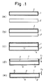
- Fig. 1 is useful to explanation of the manufacturing method according to a first embodiment of the invention.
- reference numeral 1 designates a single crystal silicon mirror wafer whose lower face (as viewed in Fig. 1) is mirror-finished, and whose upper face after grinding and polishing is made into a device formation face.
- this wafer which is hereinafter called “the bond wafer 1”
- the bond wafer 1 is subjected to an oxidation treatment whereby a silicon dioxide film 3 having a thickness of about 0.5 ⁇ m is formed all over the surface of the bond wafer 1.
- a single crystal silicon mirror wafer 2 whose upper face (as viewed in Fig. 1) is mirror-finished is prepared.
- This wafer 2 is hereinafter referred to as "the base wafer 2".
- the base wafer 2 and the bond wafer 1 are joined together with the mirror-finished faces meeting each other.
- the combined wafers 1, 2 are heated at about 500°C in a nitrogen gas atmosphere to thereby create adhesive strength between the wafers.
- the laminated wafers 1, 2 are then heated at about 1100°C in an oxidizing atmosphere for approximately 120 minutes (thermal oxidation treatment).
- a silicon dioxide film 4 hatchched in Fig. 1), which is about 0.5 ⁇ m in tickness, is formed all over the laminated wafers 1, 2.
- the laminated wafers 1, 2 are cooled, and the exposed side of the bond wafer 1 is ground until the thickness of the bond wafer 1 is reduced to a predetermined value t1, e.g. 6 ⁇ m [primary grinding; step (d) in Fig. 1].
- the wafers 1, 2 shrink more than the silicon dioxide films 3, 4 do, and as a result residual stress is created in the lamination.
- the both faces of the base wafer 2 are covered with either the oxide film 3 or the oxide film 4 which films are of roughly the same thickness (about 0.5 ⁇ m)
- the residual stress balances between the two faces of the base wafer 2 so that the thermal shrinkage amount at one face of the base wafer 2 is roughly equal to that at the other face; consequently, the base wafer 2 does not warp.
- the bond wafer 1 having a thickness t1 [Fig. 1 (d)] is further ground until the thickness is reduced to a predetermined value t2, e.g. 3 ⁇ m (secondary grinding).
- a bonded wafer 5 shown at (e) in Fig. 1 is obtained.
- the bonded wafer 5 Since the base wafer 2, whose thickness accounts mostly for the overall thickness of the bonded wafer 5, scarcely warps, the bonded wafer 5 does not warp either, and it will have a high degree of flatness. Consequently, in the subsequent processes the bonded wafer 5 facilitates smooth operation; for example, the bonded wafer 5 allows itself to be sucked by vacuum without fail.
- the solid kinked line represents the result of actual measurement of the warpage of fifty bonded wafers obtained by the method of the invention.
- the axis of abscissa represents bonded wafer Nos. (No.1 through No. 50); the axis of ordinate represents the amount of warpage by which it increased as a result of the primary grinding.
- the dashed kinked line in Fig. 2 represents the result of actual measurement of the warpage of fifty bonded wafers obtained by a conventional method.
- the average value R′ of the increase in warpage in the case of the bonded wafers obtained by a conventional manufacturing method was 87 ⁇ m; whereas the average are of the increase in warpage in the case of the bonded wafers of the present embodiment was -3 ⁇ m, which is insignificantly small.
- the method of the present invention as described in this embodiment proved to attain the objects of the invention.
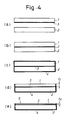
- reference numeral 1 designates a single crystal silicon mirror wafer whose lower face (as viewed in Fig. 4) is mirror-finished, and whose upper face after grinding and polishing is made into a device formation face.
- this wafer i.e., the bond wafer 1
- this wafer is subjected to an oxidation treatment whereby a silicon dioxide film 3 having a thickness of about 0.5 ⁇ m is formed over the lower face thereof.
- a single crystal silicon mirror wafer 2 that is, a base wafer 2, whose upper face (as viewed in Fig. 4) is mirror-finished is prepared.
- the base wafer 2 and the bond wafer 1 are joined together with the mirror-finished faces meeting each other.
- the combined wafers 1, 2 are heated at about 500°C in a nitrogen gas atmosphere to thereby create adhesive strength between the wafers.
- the laminated wafers 1, 2 are then heated at about 1100°C in an oxidizing atmosphere for approximately 120 minutes (thermal oxidation treatment).
- a silicon dioxide film 4 which is about 0.5 ⁇ m in thickness, is formed all over the laminated wafers 1, 2.
- the laminated wafers 1, 2 are cooled, and the exposed side of the bond wafer 1 is ground until the thickness of the bond wafer 1 is reduced to a predetermined value t1, e.g. 6 ⁇ m [primary grinding; step (d) in Fig. 4].
- the wafers 1, 2 shrink more than the silicon dioxide films 3, 4 do, and as a result residual stress is created in the lamination.
- the both faces of the base wafer 2 are covered with either the oxide film 3 or the oxide film 4 which films are of roughly the same thickness (about 0.5 ⁇ m)
- the residual stress balances between the two faces of the base wafer 2 so that the thermal shrinkage amount at one face of the base wafer 2 is roughly equal to that at the other face; consequently, the base wafer 2 does not warp.
- the bond wafer 1 having a thickness t1 [Fig. 4 (d)] is further ground until the thickness is reduced to a predetermined value t2, e.g. 3 ⁇ m (secondary grinding).
- a bonded wafer 5 shown at (e) in Fig. 4 is obtained.
- the bonded wafer 5 Since the base wafer 2, whose thickness accounts mostly for the overall thickness of the bonded wafer 5, scarcely warps, the bonded wafer 5 does not warp either, and it will have a high degree of flatness.
- a number of bonded wafers were prepared through the same procedure of this second embodiment except that the heating temperature at step (b) for wafer binding was 800 °C, 900 °C, 1000 °C, 1100 °C, and 1200°C, and the heating time was two hours.
- the tensile strength of each bonded wafer was measured with a tensile testing machine. The result is shown at (c) in Fig. 5.
- bonded wafers wherein no oxide film is formed between the bond and base wafers were prepared, and the similar tensile strength test was conducted on these bonded wafers, and the result is shown at (a) in Fig. 5.
- a number of bonded wafers were prepared wherein two layers of oxide were formed between the wafers. These were heated in the similar manner, and the same tensile strength test was conducted on these bonded wafers, and the result is shown at (b) in Fig. 5.
- a symbol ⁇ designates the tensile force with which a bonded wafer was pulled when the bonded wafer was torn and divided into the bond wafer and base wafer.
- the other symbol ⁇ designates the tensile force with which a bonded wafer was pulled when the adhesive holding the bonded wafer onto the tensile testing machine failed and the bonded wafer came off the tensile testing machine.
- results shown at (c) in Fig. 5 indicate that if an oxide film is formed only over the bond wafer, as in the present invention, such that the resulting bonded wafer has one layer of the oxide in the bonding interface, and if the bonded wafer is heated at 1100 °C or higher, a bonding strength of 800 kg/cm2 or greater is obtained.
- the results shown at (a) in Fig. 5 indicate that if there is no oxide layer at the bonding interface, the heating temperature must be 1200 °C or higher in order to obtain a bonding strength of 800 kg/cm2 or greater.
- a bonding wafer containing two layers of the oxide at the bonding interface [(b) of Fig. 5] and a bonded wafer containing one layer of the oxide at the bondeing interface [(c) of Fig. 5] were sliced by an outer diameter saw slicing machine. Then, from each bonded wafer were cut out twenty pieces each of 2mm-square pellets, which were then placed in a 25% solution of hydrogen fluoride at 25 °C for twenty minutes. The pellets were then washed with water, dried, and the remnant bonding strength was examined in the following manner.
- the bond wafer and the base wafer were pinched and pulled from each other with a small force. About a half of the pellets cut from the bonded wafer having two layers of oxide at the bonding interface were torn apart. In the case of the pellets cut from the bonded wafer having one layer of oxide at the bonding interface, none was torn apart by the pulling. Cross section of the bonding interface of these pellets of the present invention were observed with a microscope, and it was confirmed that the corrosion by the etching agent did not reach the middle portion of the bonding interface, or more particularly speaking the corrosion did not progress deep into the interface between the base wafer and the oxide layer of the bond wafer.
- a bonded wafer made by the method of the present invention has another advantage.
- a device such as an integrated circuit device is formed on the bond wafer of a bonded wafer by a conventional procedure.
- the bonded wafer of the invention in which the oxide layer is originally formed over the bond wafer provides a better dielectric strength and other electric properties to the integrated circuit device by virtue of the fact that the device formation face of the bond wafer is entirely covered with the dielectric oxide film.
- the heating for creating adhesion effect and the heating for thermal oxidation constitute two different steps in the invention, it is possible to combine the adhesion step with the oxidation step into one step.
Abstract
Description
- This invention relates to a method of manufacturing a bonded wafer, especially a warpless bonded wafer having a high degree of flatness.
- As a method for forming a single crystal semiconductor film over a dielectric substrate, there has been known a technology which is characterized by epitaxially growing a single crystal silicon film or the like over a single crystal sapphire substrate. In this technology, however, because there exists a disagreement in lattice constant between the dielectric substrate and the silicon single crystal which is grown in vapor phase, numerous crystal defects occur in the silicon vapor-phase grown layer, and for this reason this technology is of no practical use.
- Another conventional technology of providing a single crystal film on a dielectric substrate is characterized by first forming a thermally oxidized oxide film across the surface of the silicon substrate, laying a polycrystal or amorphous silicon film over this oxide film, and applying to this an energy beam such as an electron beam or a laser beam in a manner such that the beam spot thereon is shifted along lines all in one and the same direction to thereby melt the silicon film, and then cooling and solidifying the film to obtain a monolithic single crystal film.
- Now, the technology of changing the silicon polycrystal film over the oxide film into the single crystal film by means of the laser beam or the like is disclosed, for example, in Japanese Patent Kokoku 62-34716. According to this publication, a single crystal projection is monolithically formed at a corner of the periphery of a single crystal silicon substrate, and with this projection as the seed crystal, single crystallization of the polycrystal film is effected. Although locallized growth of a single crystal is possible, owing to an interaction between the single crystal projection and the molten silicon oxide film, it is difficult to obtain a silicon single crystal film of practical use.
- Under the circumstances, bonded wafers having Si-on-insulation structure (SOI structure) have come to draw the attention of the scientists in the field. An SOI bonded wafer is made of two silicon mirror wafers which are joined together face to face, with an oxide layer formed between them.
- Fig. 3 shows an example of the procedure of manufacturing such silicon bonded wafer. At the stage (a), two semiconductor mirror wafers of silicon single crystal are prepared. The one (hereinafter referred to as "the bond wafer") 101 whose upper face, as viewed in Fig. 3, is to be made into the device formation face is subjected to a thermal oxidation treatment whereby a
thin oxide film 103 of silicon dioxide is formed throughout the entire surface, or on both main surfaces, of thebond wafer 101. Theother mirror wafer 102 shall be referred to as "the base wafer", and is employed mainly for a protective purpose, that is, for securing mechanical strength of the final bonded wafer. - At the next stage (b), the two
wafers bond wafer 101 is ground until the thickness of thebond wafer 101 becomes several µm (the hatched portion of thebond wafer 101 is ground off). As the result, abonded wafer 105 is obtained, as shown at (d) of Fig. 3. - When, for example, the
bonded wafer 105 was made in the manner as described above, the intermediate silicon dioxide layer is fixed between the twowafers wafer 105 is cooled thereafter, residual stress (tensile stress mainly) is accumulated in the wafer, since the coefficient of thermal expansion (or the coefficient of thermal contraction) of silicon single crystal is greater than that of silicon dioxide. When thebond wafer 101 is ground thinner, the residual stress contained in thebond wafer 101 is mostly relieved and becomes negligible compared with that in thebase wafer 102, and as a result, the residual stress in thebase wafer 102, especially that accumulated near theoxide film 103, causes thebonded wafer 105 to warp as shown at (d) of Fig. 3. In particular, the base wafer 102 without theoxide film 103 shrinks greater than thebond wafer 101. Thus, thebonded wafer 105 arches in a manner such that the side of thebond wafer 101 forms the convex, and the magnitude of warpage is generally 100 - 200 µm. - If the
bonded wafer 105 is warped, as shown at (d) of Fig. 3, problems are experienced when thebonded wafer 105 has to be attached to the level block of a grinder by suction or with wax for further grinding of thebond wafer 101, because it is difficult to hold the warped wafer onto the flat surface of the level block, and in the later processes, such as photolithography process, after the further grinding, the warped bondedwafer 105 causes such inconveniences as difficulty in its setting to various wafer stages and deformed circuit pattern exposure onto a photoresist. - A method was proposed wherein the bond wafer and/or the base wafer are/is warped beforehand in a manner that compensates the warpage which occurs as the bonded wafer is thermally oxidized and cool. However, this method does not sufficiently remove the warpage from the bonded wafer.
- Now, in a bonded wafer, it is necessary that the bonding strength between the bond wafer and the base wafer is sufficiently high throughout the bonded face; otherwise, areas where bonding is not effected called voids are formed in the bonding interface, which results in poor yield of products. In order to achieve complete bonding between the wafers, and for certain other reasons, the faces of wafers to be bonded to each other is polished to a specular gloss finish.
- Incidentally, the voids in a bonded wafer can be detected by means of such known methods as infrared ray transmission method, ultrasonic flaw detection method, and X-ray diffraction micrography method.
- In the process of manufacturing bonded wafers, each bonded wafer is etched with an etching liquid such as hydrogen fluoride for the purpose of removing the oxide film formed over the wafer surfaces. If the corrosion resistance of the bonding interface against the etching liquid is not sufficiently strong, an inconvenience experienced is that the bonding interface fails to hold the wafers together and a pattern formed on the bond wafer can come off during the device formation processes.
- The present invention was made in view of the above-stated problems; therefore, it is an object of the invention to provide a method for manufacturing a bonded wafer which can provide a warpless bonded wafer having a high degree of flatness even after the bond wafer is ground thin.
- It is another object of the invention to provide a method for manufacturing a bonded wafer that can provide a bonded wafer in which the bonding strength between the bond wafer and the base wafer is sufficiently high throughout the bonded face, and the corrosion resistance of the bonding interface against an etching liquid is sufficiently great.
- There are three conceivable manners in which a bonded wafer is produced wherein an oxide layer is sandwiched between the bond and base wafers: that is, (1) form oxide layer over the base wafer, and attach the bond wafer onto the oxide layer of the base wafer; (2) form an oxide layer over the bond wafer, and attach the base wafer onto the oxide layer of the bond wafer; (3) form an oxide layer over both the bond wafer and the base wafer, and attach the two wafers together with the oxide layer inbetween.
- The present inventors had supposed that probably one of these manners would be more effective than others in giving high bonding strength between the wafers and improving corrosion resistance of the bonding interface against the etching liquid. To confirm their supposition, the inventors conducted various experiments and came to a conclusion that if the manner (2) is observed the best result is obtained.
- In order to attain the objects of the invention, the inventors propose a method of manufacturing a bonded wafer which comprises the steps of: preparing a first mirror wafer at least one face of which has specular gloss; preparing a second mirror wafer at least one face of which has specular gloss; forming a first oxide film over at least one face of the second mirror wafer which face has specular gloss; joining the first and second mirror wafers face to face in a manner such that the first oxide film formed on a specular-glossed face of the second mirror wafer is sandwiched between a specular-glossed face of the first mirror wafer and the second mirror wafer; heating the thus joined wafers at a high temperature to thereby create bonding strength between the two wafers; subjecting the two joined wafers to a thermal oxidation treatment to thereby form a second oxide film all over the joined wafers; and grinding the external face of either the first or second wafer until the wafer selected to be ground becomes a thin film.
- In a preferred embodiment of the invention, the inventors propose that the wafer selected to be ground at the end of the method is the second wafer.
- In an embodiment of the invention, the first oxide film is formed all over the second wafer.
- Further, it is proposed as a still more preferred embodiment that the first oxide film is formed only over one face of the second wafer which face has specular gloss.
- It is also preferable if the thickness of the second oxide film is nearly equal to the thickness of the first oxide film.
- In a case where the bonded wafer of the invention is used as a substrate for a semiconductor device such as a semiconductor integrated circuit, the wafer to be ground and made into a thin film should be selected from those which have physical and electric properties that correspond to the properties of the semiconductor device. Incidentally, the thickness of the oxide film which is formed after the bonding of the wafers is preferably close to the thickness of the oxide film sandwiched between the two wafers.
- According to the invention, the first wafer (base wafer) has its both faces covered with an oxide film as of the time when the second wafer (bond wafer) is ground and thinned to a film, so that the thermal contraction coefficient at one face of the first wafer is roughly equal to that at the other face thereof; accordingly, the residual stress distribution in the first wafer becomes such that the magnitude of the residual stress at one face is roughly equal to that at the other face. As a result, the first wafer does not warp and a warpless bonded wafer having a high degree of flatness is obtained.
- These together with other objects and advantages which will become subsequently apparent reside in the details of operation as more fully hereinafter described and claimed, reference being made to the accompanying drawings forming a part hereof.
- Fig. 1 is a drawing useful in explaining the procedure of the first embodiment of the invention;
- Fig. 2 is a graph showing the result of a measurement of the warpage of the bonded wafers of the invention compared with the result obtained of the bonded wafers fabricated by a conventional method;
- Fig. 3 is a drawing useful in explaining the procedure of a conventional method for manufacturing a bonded wafer;
- Fig. 4 is a drawing useful in explaining the procedure of the second embodiment of the invention; and
- Fig. 5 is a graph showing the result of a tension test conducted on different kinds of bonded wafers.
- Now, embodiments of the invention will be described with reference to the attached drawings.
- Fig. 1 is useful to explanation of the manufacturing method according to a first embodiment of the invention. In Fig. 1 reference numeral 1 designates a single crystal silicon mirror wafer whose lower face (as viewed in Fig. 1) is mirror-finished, and whose upper face after grinding and polishing is made into a device formation face. At step (a) in Fig. 1, this wafer, which is hereinafter called "the bond wafer 1", is subjected to an oxidation treatment whereby a
silicon dioxide film 3 having a thickness of about 0.5 µm is formed all over the surface of the bond wafer 1. Besides this bond wafer 1, a single crystalsilicon mirror wafer 2 whose upper face (as viewed in Fig. 1) is mirror-finished is prepared. Thiswafer 2 is hereinafter referred to as "thebase wafer 2". - At step (b) in Fig. 1, the
base wafer 2 and the bond wafer 1 are joined together with the mirror-finished faces meeting each other. Then, the combinedwafers 1, 2 are heated at about 500°C in a nitrogen gas atmosphere to thereby create adhesive strength between the wafers. The laminatedwafers 1, 2 are then heated at about 1100°C in an oxidizing atmosphere for approximately 120 minutes (thermal oxidation treatment). As a result, a silicon dioxide film 4 (hatched in Fig. 1), which is about 0.5 µm in tickness, is formed all over thelaminated wafers 1, 2. - Next, the
laminated wafers 1, 2 are cooled, and the exposed side of the bond wafer 1 is ground until the thickness of the bond wafer 1 is reduced to a predetermined value t1, e.g. 6 µm [primary grinding; step (d) in Fig. 1]. - As it is earlier explained with reference to Fig. 3, when the laminated wafers are cooled, the
wafers 1, 2 shrink more than thesilicon dioxide films 3, 4 do, and as a result residual stress is created in the lamination. However, unlike the case of Fig. 3, in the present embodiment, since the both faces of thebase wafer 2 are covered with either theoxide film 3 or the oxide film 4 which films are of roughly the same thickness (about 0.5 µm), the residual stress balances between the two faces of thebase wafer 2 so that the thermal shrinkage amount at one face of thebase wafer 2 is roughly equal to that at the other face; consequently, thebase wafer 2 does not warp. - The bond wafer 1 having a thickness t1 [Fig. 1 (d)] is further ground until the thickness is reduced to a predetermined value t2, e.g. 3 µm (secondary grinding). Thus, a bonded
wafer 5 shown at (e) in Fig. 1 is obtained. - Since the
base wafer 2, whose thickness accounts mostly for the overall thickness of the bondedwafer 5, scarcely warps, the bondedwafer 5 does not warp either, and it will have a high degree of flatness. Consequently, in the subsequent processes the bondedwafer 5 facilitates smooth operation; for example, the bondedwafer 5 allows itself to be sucked by vacuum without fail. - In Fig. 2, the solid kinked line represents the result of actual measurement of the warpage of fifty bonded wafers obtained by the method of the invention. The axis of abscissa represents bonded wafer Nos. (No.1 through No. 50); the axis of ordinate represents the amount of warpage by which it increased as a result of the primary grinding. The dashed kinked line in Fig. 2 represents the result of actual measurement of the warpage of fifty bonded wafers obtained by a conventional method.
- According to the graphs in Fig. 2, the average value R′ of the increase in warpage in the case of the bonded wafers obtained by a conventional manufacturing method was 87 µm; whereas the average are of the increase in warpage in the case of the bonded wafers of the present embodiment was -3µm, which is insignificantly small. Thus, the method of the present invention as described in this embodiment proved to attain the objects of the invention.
- Now, with reference to Fig. 4, the manufacturing method according to a second embodiment of the invention will be explained. In fig. 4, the reference numerals identical to those in Fig. 1 designate the same elements of the first embodiment; therefore, for example, reference numeral 1 designates a single crystal silicon mirror wafer whose lower face (as viewed in Fig. 4) is mirror-finished, and whose upper face after grinding and polishing is made into a device formation face. At step (a) in Fig. 4, this wafer, i.e., the bond wafer 1, is subjected to an oxidation treatment whereby a
silicon dioxide film 3 having a thickness of about 0.5µm is formed over the lower face thereof. Besides this bond wafer 1, a single crystalsilicon mirror wafer 2, that is, abase wafer 2, whose upper face (as viewed in Fig. 4) is mirror-finished is prepared. - At step (b) in Fig. 4, the
base wafer 2 and the bond wafer 1 are joined together with the mirror-finished faces meeting each other. Then, the combinedwafers 1, 2 are heated at about 500°C in a nitrogen gas atmosphere to thereby create adhesive strength between the wafers. Thelaminated wafers 1, 2 are then heated at about 1100°C in an oxidizing atmosphere for approximately 120 minutes (thermal oxidation treatment). As a result, a silicon dioxide film 4, which is about 0.5 µm in thickness, is formed all over thelaminated wafers 1, 2. - Next, the
laminated wafers 1, 2 are cooled, and the exposed side of the bond wafer 1 is ground until the thickness of the bond wafer 1 is reduced to a predetermined value t1, e.g. 6 µm [primary grinding; step (d) in Fig. 4]. - When the laminated wafers are cooled, the
wafers 1, 2 shrink more than thesilicon dioxide films 3, 4 do, and as a result residual stress is created in the lamination. However, since in the present embodiment the both faces of thebase wafer 2 are covered with either theoxide film 3 or the oxide film 4 which films are of roughly the same thickness (about 0.5µm), the residual stress balances between the two faces of thebase wafer 2 so that the thermal shrinkage amount at one face of thebase wafer 2 is roughly equal to that at the other face; consequently, thebase wafer 2 does not warp. - The bond wafer 1 having a thickness t1 [Fig. 4 (d)] is further ground until the thickness is reduced to a predetermined value t2, e.g. 3 µm (secondary grinding). Thus, a bonded
wafer 5 shown at (e) in Fig. 4 is obtained. - Since the
base wafer 2, whose thickness accounts mostly for the overall thickness of the bondedwafer 5, scarcely warps, the bondedwafer 5 does not warp either, and it will have a high degree of flatness. - In order to compare the bonding strength of the thus obtained bonded
wafer 5, a number of bonded wafers were prepared through the same procedure of this second embodiment except that the heating temperature at step (b) for wafer binding was 800 °C, 900 °C, 1000 °C, 1100 °C, and 1200°C, and the heating time was two hours. The tensile strength of each bonded wafer was measured with a tensile testing machine. The result is shown at (c) in Fig. 5. Under the same heating conditions, bonded wafers wherein no oxide film is formed between the bond and base wafers were prepared, and the similar tensile strength test was conducted on these bonded wafers, and the result is shown at (a) in Fig. 5. Further, by attaching an oxide film-covered face of a bond wafer to an oxide film-covered face of a base wafer, a number of bonded wafers were prepared wherein two layers of oxide were formed between the wafers. These were heated in the similar manner, and the same tensile strength test was conducted on these bonded wafers, and the result is shown at (b) in Fig. 5. In Fig. 5, a symbol ● designates the tensile force with which a bonded wafer was pulled when the bonded wafer was torn and divided into the bond wafer and base wafer. The other symbol ○ designates the tensile force with which a bonded wafer was pulled when the adhesive holding the bonded wafer onto the tensile testing machine failed and the bonded wafer came off the tensile testing machine. - The results shown at (c) in Fig. 5 indicate that if an oxide film is formed only over the bond wafer, as in the present invention, such that the resulting bonded wafer has one layer of the oxide in the bonding interface, and if the bonded wafer is heated at 1100 °C or higher, a bonding strength of 800 kg/cm² or greater is obtained. The results shown at (a) in Fig. 5 indicate that if there is no oxide layer at the bonding interface, the heating temperature must be 1200 °C or higher in order to obtain a bonding strength of 800 kg/cm² or greater.
- The results shown at (b) in Fig. 5 indicate that if two layers of oxide are formed at the bonding interface, the heating temperature must be 1200 °C or higher in order to obtain a bonding strength of 800 kg/cm² or greater.
- It follows from this comparative tests that only the method of the present invention provides a bonded wafer having a bonding strength of 800 kg/cm² or greater, under the condition that the heating temperature is not higher than 1100 °C.
- Another test was conducted to find the corrosion resistance of the bonding interface of each of these bonded wafers against an etching agent (hydrogen fluoride). The result was such that the bonded wafers of the present invention retained high corrosion resistance at the bonding interface. However, the bonded wafers prepared in the manners different from the present invention did not show sufficiently high corrosion resistance at the bonding interface.
- In order to compare the durability of the bonding interface against the etching agent, a bonding wafer containing two layers of the oxide at the bonding interface [(b) of Fig. 5] and a bonded wafer containing one layer of the oxide at the bondeing interface [(c) of Fig. 5] were sliced by an outer diameter saw slicing machine. Then, from each bonded wafer were cut out twenty pieces each of 2mm-square pellets, which were then placed in a 25% solution of hydrogen fluoride at 25 °C for twenty minutes. The pellets were then washed with water, dried, and the remnant bonding strength was examined in the following manner.
- Using two pairs of pincettes, the bond wafer and the base wafer were pinched and pulled from each other with a small force. About a half of the pellets cut from the bonded wafer having two layers of oxide at the bonding interface were torn apart. In the case of the pellets cut from the bonded wafer having one layer of oxide at the bonding interface, none was torn apart by the pulling. Cross section of the bonding interface of these pellets of the present invention were observed with a microscope, and it was confirmed that the corrosion by the etching agent did not reach the middle portion of the bonding interface, or more particularly speaking the corrosion did not progress deep into the interface between the base wafer and the oxide layer of the bond wafer.
- A bonded wafer made by the method of the present invention has another advantage. Suppose that a device such as an integrated circuit device is formed on the bond wafer of a bonded wafer by a conventional procedure. Compared with a bonded wafer in which the oxide layer is originally formed over the base wafer, the bonded wafer of the invention in which the oxide layer is originally formed over the bond wafer, provides a better dielectric strength and other electric properties to the integrated circuit device by virtue of the fact that the device formation face of the bond wafer is entirely covered with the dielectric oxide film.
- Incidentally, in the two embodiments the heating for creating adhesion effect and the heating for thermal oxidation constitute two different steps in the invention, it is possible to combine the adhesion step with the oxidation step into one step.
- Obviously many modifications and variations of the present invention are possible in the light of the above teachings. It is therefore to be understood that within the scope of the appended claims the invention may be practiced otherwise than as specifically described.
Claims (7)
- A method of manufacturing a bonded wafer which comprises the steps of: preparing a first mirror wafer at least one face of which has specular gloss; preparing a second mirror wafer at least one face of which has specular gloss; forming a first oxide film over at least one face of said second mirror wafer which face has specular gloss; joining said first and second mirror wafers face to face in a manner such that said first oxide film formed on a specular-glossed face of said second mirror wafer is sandwiched between a specular-glossed face of said first mirror wafer and said second mirror wafer; heating the thus joined wafers at a high temperature to thereby create bonding strength between said two wafers; subjecting said two joined wafers to a thermal oxidation treatment to thereby form a second oxide film all over said joined wafers; and grinding the external face of either said first or second wafer until the wafer selected to be ground becomes a thin film.
- A method as claimed in Claim 1 wherein the wafer selected to be ground at the end of the method is said second wafer.
- A method as claimed in Claim 1 wherein said first oxide film is formed all over said second mirror wafer.
- A method as claimed in Claim 1 wherein said first oxide film is formed only over one face of said second mirror wafer which face has specular gloss.
- A method as claimed in Claim 1 wherein the thickness of said first oxide film is nearly equal to the thickness of said second oxide film.
- A method as claimed in Claim 1 wherein the temperature for heating the joined wafers for creating bonding strength between the wafers is about 1100 °C.
- A silicon single crystal bonded wafer made by the method of Claim 1.
Applications Claiming Priority (4)
| Application Number | Priority Date | Filing Date | Title |
|---|---|---|---|
| JP2045778A JPH0795505B2 (en) | 1990-02-28 | 1990-02-28 | Method for manufacturing bonded wafer |
| JP45776/90 | 1990-02-28 | ||
| JP2045776A JPH0680624B2 (en) | 1990-02-28 | 1990-02-28 | Method for manufacturing bonded wafer |
| JP45778/90 | 1990-02-28 |
Publications (2)
| Publication Number | Publication Date |
|---|---|
| EP0444943A1 true EP0444943A1 (en) | 1991-09-04 |
| EP0444943B1 EP0444943B1 (en) | 1997-05-21 |
Family
ID=26385840
Family Applications (1)
| Application Number | Title | Priority Date | Filing Date |
|---|---|---|---|
| EP91301680A Expired - Lifetime EP0444943B1 (en) | 1990-02-28 | 1991-02-28 | A method of manufacturing a bonded wafer |
Country Status (2)
| Country | Link |
|---|---|
| EP (1) | EP0444943B1 (en) |
| DE (1) | DE69126153T2 (en) |
Cited By (9)
| Publication number | Priority date | Publication date | Assignee | Title |
|---|---|---|---|---|
| EP0561532A2 (en) * | 1992-03-16 | 1993-09-22 | AT&T Corp. | Method of manufacturing an integrated circuit including planarizing a wafer |
| FR2689682A1 (en) * | 1992-04-01 | 1993-10-08 | Fraunhofer Ges Forschung | Process for producing a monocrystalline silicon layer on a buried dielectric |
| WO1993026041A1 (en) * | 1992-06-17 | 1993-12-23 | Harris Corporation | Bonded wafer processing |
| EP0628995A1 (en) * | 1993-06-07 | 1994-12-14 | Canon Kabushiki Kaisha | Semiconductor substrate and method of manufacturing same |
| DE19803852A1 (en) * | 1998-01-31 | 1999-08-12 | Bosch Gmbh Robert | Two-side oxidized silicon wafer for production of SOI devices, optical waveguide structures and micro-systems |
| FR2777115A1 (en) * | 1998-04-07 | 1999-10-08 | Commissariat Energie Atomique | PROCESS FOR TREATING SEMICONDUCTOR SUBSTRATES AND STRUCTURES OBTAINED BY THIS PROCESS |
| WO2006128953A2 (en) * | 2005-06-02 | 2006-12-07 | Okmetic Oyj | Thinning op a si wafer for mems-sensors applications |
| US8053334B2 (en) | 2007-05-29 | 2011-11-08 | Shin-Etsu Handotai Co., Ltd. | Method for forming silicon oxide film of SOI wafer |
| US9401183B2 (en) | 1997-04-04 | 2016-07-26 | Glenn J. Leedy | Stacked integrated memory device |
Families Citing this family (9)
| Publication number | Priority date | Publication date | Assignee | Title |
|---|---|---|---|---|
| US6484585B1 (en) | 1995-02-28 | 2002-11-26 | Rosemount Inc. | Pressure sensor for a pressure transmitter |
| US5637802A (en) | 1995-02-28 | 1997-06-10 | Rosemount Inc. | Capacitive pressure sensor for a pressure transmitted where electric field emanates substantially from back sides of plates |
| US6561038B2 (en) | 2000-01-06 | 2003-05-13 | Rosemount Inc. | Sensor with fluid isolation barrier |
| US6520020B1 (en) | 2000-01-06 | 2003-02-18 | Rosemount Inc. | Method and apparatus for a direct bonded isolated pressure sensor |
| US6505516B1 (en) | 2000-01-06 | 2003-01-14 | Rosemount Inc. | Capacitive pressure sensing with moving dielectric |
| CN1151367C (en) | 2000-01-06 | 2004-05-26 | 罗斯蒙德公司 | Grain growth of electrical interconnection for microelectromechanical systems (MEMS) |
| US6508129B1 (en) | 2000-01-06 | 2003-01-21 | Rosemount Inc. | Pressure sensor capsule with improved isolation |
| JP5418564B2 (en) | 2011-09-29 | 2014-02-19 | 信越半導体株式会社 | Method for calculating warpage of bonded SOI wafer, and method for manufacturing bonded SOI wafer |
| DE102014219648A1 (en) | 2014-09-29 | 2015-10-15 | Carl Zeiss Smt Gmbh | Method for producing a mirror element |
Citations (2)
| Publication number | Priority date | Publication date | Assignee | Title |
|---|---|---|---|---|
| EP0192488A2 (en) * | 1985-02-20 | 1986-08-27 | Kabushiki Kaisha Toshiba | Semiconductor sensor and method of manufacturing the same |
| EP0337556A1 (en) * | 1988-04-13 | 1989-10-18 | Koninklijke Philips Electronics N.V. | Method of manufacturing a semiconductor body |
Family Cites Families (1)
| Publication number | Priority date | Publication date | Assignee | Title |
|---|---|---|---|---|
| JPS6173345A (en) * | 1984-09-19 | 1986-04-15 | Toshiba Corp | Semiconductor device |
-
1991
- 1991-02-28 DE DE1991626153 patent/DE69126153T2/en not_active Expired - Fee Related
- 1991-02-28 EP EP91301680A patent/EP0444943B1/en not_active Expired - Lifetime
Patent Citations (2)
| Publication number | Priority date | Publication date | Assignee | Title |
|---|---|---|---|---|
| EP0192488A2 (en) * | 1985-02-20 | 1986-08-27 | Kabushiki Kaisha Toshiba | Semiconductor sensor and method of manufacturing the same |
| EP0337556A1 (en) * | 1988-04-13 | 1989-10-18 | Koninklijke Philips Electronics N.V. | Method of manufacturing a semiconductor body |
Non-Patent Citations (5)
| Title |
|---|
| EXTENDED ABSTRACTS OF THE 20TH CONF. ON SOLID STATE DEVICES AND MATERIALS 24 August 1988, TOKYO pages 197 - 200; XU XIAO-LI et al.: "Si on SiO2 by Solid State Diffusion Bonding (SSDB) technology" * |
| FUJITSU-SCIENTIFIC AND TECHNICAL JOURNAL. vol. 24, no. 4, 1988, KAWASAKI JP pages 408 - 417; Hiroshi GOTOU et al.: "SOI-device on bonded wafer" * |
| PATENT ABSTRACTS OF JAPAN vol. 12, no. 447 (E-685) 24 November 1988, & JP-A-63 175484 (YOKOGAWA ELECTRIC CORP.) 19 July 1988, * |
| PATENT ABSTRACTS OF JAPAN vol. 13, no. 525 (E-850) 22 November 1989, & JP-A-01 215041 (SONY CORP.) 29 August 1989, * |
| PATENT ABSTRACTS OF JAPAN vol. 14, no. 99 (E-893) 22 February 1990, & JP-A-01 302740 (TOSHIBA CORP.) 06 December 1989, * |
Cited By (17)
| Publication number | Priority date | Publication date | Assignee | Title |
|---|---|---|---|---|
| EP0561532A3 (en) * | 1992-03-16 | 1997-08-20 | American Telephone & Telegraph | Method of manufacturing an integrated circuit including planarizing a wafer |
| EP0561532A2 (en) * | 1992-03-16 | 1993-09-22 | AT&T Corp. | Method of manufacturing an integrated circuit including planarizing a wafer |
| FR2689682A1 (en) * | 1992-04-01 | 1993-10-08 | Fraunhofer Ges Forschung | Process for producing a monocrystalline silicon layer on a buried dielectric |
| WO1993020584A1 (en) * | 1992-04-01 | 1993-10-14 | Fraunhofer-Gesellschaft zur Förderung der angewandten Forschung e.V. | Process for producing a monocrystalline silicon layer on an embedded dielectric |
| WO1993026041A1 (en) * | 1992-06-17 | 1993-12-23 | Harris Corporation | Bonded wafer processing |
| US5780311A (en) * | 1992-06-17 | 1998-07-14 | Harris Corporation | bonded wafer processing |
| US5801084A (en) * | 1992-06-17 | 1998-09-01 | Harris Corporation | Bonded wafer processing |
| EP0628995A1 (en) * | 1993-06-07 | 1994-12-14 | Canon Kabushiki Kaisha | Semiconductor substrate and method of manufacturing same |
| US9401183B2 (en) | 1997-04-04 | 2016-07-26 | Glenn J. Leedy | Stacked integrated memory device |
| DE19803852A1 (en) * | 1998-01-31 | 1999-08-12 | Bosch Gmbh Robert | Two-side oxidized silicon wafer for production of SOI devices, optical waveguide structures and micro-systems |
| DE19803852C2 (en) * | 1998-01-31 | 2003-12-18 | Bosch Gmbh Robert | Process for the production of silicon wafers oxidized on both sides |
| WO1999052145A1 (en) * | 1998-04-07 | 1999-10-14 | Commissariat A L'energie Atomique | Heat treatment method for semiconductor substrates |
| US6403450B1 (en) | 1998-04-07 | 2002-06-11 | Commissariat A L'energie Atomique | Heat treatment method for semiconductor substrates |
| FR2777115A1 (en) * | 1998-04-07 | 1999-10-08 | Commissariat Energie Atomique | PROCESS FOR TREATING SEMICONDUCTOR SUBSTRATES AND STRUCTURES OBTAINED BY THIS PROCESS |
| WO2006128953A2 (en) * | 2005-06-02 | 2006-12-07 | Okmetic Oyj | Thinning op a si wafer for mems-sensors applications |
| WO2006128953A3 (en) * | 2005-06-02 | 2007-02-01 | Okmetic Oyj | Thinning op a si wafer for mems-sensors applications |
| US8053334B2 (en) | 2007-05-29 | 2011-11-08 | Shin-Etsu Handotai Co., Ltd. | Method for forming silicon oxide film of SOI wafer |
Also Published As
| Publication number | Publication date |
|---|---|
| EP0444943B1 (en) | 1997-05-21 |
| DE69126153T2 (en) | 1998-01-08 |
| DE69126153D1 (en) | 1997-06-26 |
Similar Documents
| Publication | Publication Date | Title |
|---|---|---|
| EP0444943B1 (en) | A method of manufacturing a bonded wafer | |
| JP4388741B2 (en) | Method for transferring semiconductor thin layer and method for manufacturing donor wafer used therefor | |
| EP0706714B1 (en) | Soi substrate fabrication | |
| EP0584778B1 (en) | Method of preparing a semiconductor substrate | |
| JP4167065B2 (en) | Method for forming a laminated structure | |
| US5266824A (en) | SOI semiconductor substrate | |
| EP0854500B1 (en) | Method of manufacturing a bonded substrate | |
| US20090311477A1 (en) | Compliant Substrate In Particular For Hetero-Epitaxial Depositing | |
| US20060049487A1 (en) | Semiconductor device and method of manufacturing the same | |
| US6355541B1 (en) | Method for transfer of thin-film of silicon carbide via implantation and wafer bonding | |
| US5240883A (en) | Method of fabricating soi substrate with uniform thin silicon film | |
| JP3327180B2 (en) | Method of forming oxide film on SOI layer, method of manufacturing bonded wafer, and bonded wafer manufactured by this method | |
| JPH098124A (en) | Insulation separation substrate and its manufacture | |
| US6614065B2 (en) | Use of membrane properties to reduce residual stress in an interlayer region | |
| JP2621325B2 (en) | SOI substrate and manufacturing method thereof | |
| EP0860862A2 (en) | Method of manufacturing a bonding substrate | |
| JP3921823B2 (en) | Manufacturing method of SOI wafer and SOI wafer | |
| JP3030545B2 (en) | Manufacturing method of bonded wafer | |
| JPH05275300A (en) | Method of joining semiconductor wafers | |
| JPH07249573A (en) | Manufacture of semiconductor substrate | |
| JPH0680624B2 (en) | Method for manufacturing bonded wafer | |
| JPH03250617A (en) | Manufacture of bonded wafer | |
| JP2609198B2 (en) | Semiconductor substrate manufacturing method | |
| JP2820120B2 (en) | Semiconductor substrate manufacturing method | |
| JPH0563071A (en) | Manufacture of dielectric isolation substrate |
Legal Events
| Date | Code | Title | Description |
|---|---|---|---|
| PUAI | Public reference made under article 153(3) epc to a published international application that has entered the european phase |
Free format text: ORIGINAL CODE: 0009012 |
|
| AK | Designated contracting states |
Kind code of ref document: A1 Designated state(s): DE FR GB |
|
| 17P | Request for examination filed |
Effective date: 19910815 |
|
| 17Q | First examination report despatched |
Effective date: 19940816 |
|
| GRAG | Despatch of communication of intention to grant |
Free format text: ORIGINAL CODE: EPIDOS AGRA |
|
| GRAH | Despatch of communication of intention to grant a patent |
Free format text: ORIGINAL CODE: EPIDOS IGRA |
|
| GRAH | Despatch of communication of intention to grant a patent |
Free format text: ORIGINAL CODE: EPIDOS IGRA |
|
| GRAA | (expected) grant |
Free format text: ORIGINAL CODE: 0009210 |
|
| AK | Designated contracting states |
Kind code of ref document: B1 Designated state(s): DE FR GB |
|
| ET | Fr: translation filed | ||
| REF | Corresponds to: |
Ref document number: 69126153 Country of ref document: DE Date of ref document: 19970626 |
|
| PLBE | No opposition filed within time limit |
Free format text: ORIGINAL CODE: 0009261 |
|
| STAA | Information on the status of an ep patent application or granted ep patent |
Free format text: STATUS: NO OPPOSITION FILED WITHIN TIME LIMIT |
|
| 26N | No opposition filed | ||
| PGFP | Annual fee paid to national office [announced via postgrant information from national office to epo] |
Ref country code: GB Payment date: 19990304 Year of fee payment: 9 |
|
| PG25 | Lapsed in a contracting state [announced via postgrant information from national office to epo] |
Ref country code: GB Free format text: LAPSE BECAUSE OF NON-PAYMENT OF DUE FEES Effective date: 20000228 |
|
| GBPC | Gb: european patent ceased through non-payment of renewal fee |
Effective date: 20000228 |
|
| PGFP | Annual fee paid to national office [announced via postgrant information from national office to epo] |
Ref country code: FR Payment date: 20010213 Year of fee payment: 11 |
|
| PGFP | Annual fee paid to national office [announced via postgrant information from national office to epo] |
Ref country code: DE Payment date: 20010221 Year of fee payment: 11 |
|
| PG25 | Lapsed in a contracting state [announced via postgrant information from national office to epo] |
Ref country code: DE Free format text: LAPSE BECAUSE OF NON-PAYMENT OF DUE FEES Effective date: 20020903 |
|
| PG25 | Lapsed in a contracting state [announced via postgrant information from national office to epo] |
Ref country code: FR Free format text: LAPSE BECAUSE OF NON-PAYMENT OF DUE FEES Effective date: 20021031 |
|
| REG | Reference to a national code |
Ref country code: FR Ref legal event code: ST |