EP0443752A2 - Block-cipher cryptographic device based upon a pseudorandom nonlinear sequence generator - Google Patents
Block-cipher cryptographic device based upon a pseudorandom nonlinear sequence generator Download PDFInfo
- Publication number
- EP0443752A2 EP0443752A2 EP91300986A EP91300986A EP0443752A2 EP 0443752 A2 EP0443752 A2 EP 0443752A2 EP 91300986 A EP91300986 A EP 91300986A EP 91300986 A EP91300986 A EP 91300986A EP 0443752 A2 EP0443752 A2 EP 0443752A2
- Authority
- EP
- European Patent Office
- Prior art keywords
- data
- keystream
- cycles
- shift register
- segregated
- Prior art date
- Legal status (The legal status is an assumption and is not a legal conclusion. Google has not performed a legal analysis and makes no representation as to the accuracy of the status listed.)
- Granted
Links
Images

Classifications
-
- H—ELECTRICITY
- H04—ELECTRIC COMMUNICATION TECHNIQUE
- H04L—TRANSMISSION OF DIGITAL INFORMATION, e.g. TELEGRAPHIC COMMUNICATION
- H04L9/00—Cryptographic mechanisms or cryptographic arrangements for secret or secure communications; Network security protocols
- H04L9/06—Cryptographic mechanisms or cryptographic arrangements for secret or secure communications; Network security protocols the encryption apparatus using shift registers or memories for block-wise or stream coding, e.g. DES systems or RC4; Hash functions; Pseudorandom sequence generators
- H04L9/065—Encryption by serially and continuously modifying data stream elements, e.g. stream cipher systems, RC4, SEAL or A5/3
- H04L9/0656—Pseudorandom key sequence combined element-for-element with data sequence, e.g. one-time-pad [OTP] or Vernam's cipher
- H04L9/0662—Pseudorandom key sequence combined element-for-element with data sequence, e.g. one-time-pad [OTP] or Vernam's cipher with particular pseudorandom sequence generator
- H04L9/0668—Pseudorandom key sequence combined element-for-element with data sequence, e.g. one-time-pad [OTP] or Vernam's cipher with particular pseudorandom sequence generator producing a non-linear pseudorandom sequence
-
- H—ELECTRICITY
- H04—ELECTRIC COMMUNICATION TECHNIQUE
- H04L—TRANSMISSION OF DIGITAL INFORMATION, e.g. TELEGRAPHIC COMMUNICATION
- H04L9/00—Cryptographic mechanisms or cryptographic arrangements for secret or secure communications; Network security protocols
- H04L9/06—Cryptographic mechanisms or cryptographic arrangements for secret or secure communications; Network security protocols the encryption apparatus using shift registers or memories for block-wise or stream coding, e.g. DES systems or RC4; Hash functions; Pseudorandom sequence generators
- H04L9/0618—Block ciphers, i.e. encrypting groups of characters of a plain text message using fixed encryption transformation
- H04L9/0625—Block ciphers, i.e. encrypting groups of characters of a plain text message using fixed encryption transformation with splitting of the data block into left and right halves, e.g. Feistel based algorithms, DES, FEAL, IDEA or KASUMI
-
- H—ELECTRICITY
- H04—ELECTRIC COMMUNICATION TECHNIQUE
- H04L—TRANSMISSION OF DIGITAL INFORMATION, e.g. TELEGRAPHIC COMMUNICATION
- H04L2209/00—Additional information or applications relating to cryptographic mechanisms or cryptographic arrangements for secret or secure communication H04L9/00
- H04L2209/12—Details relating to cryptographic hardware or logic circuitry
Definitions
- the present invention generally pertains to block-cipher cryptographic devices.
- Block-cipher cryptographic devices based upon the DES (Data Encryption Standard) algorithm are often used when a high degree of encryption security is required.
- DES Data Encryption Standard
- encryption/decryption products containing a block-cipher cryptographic device based upon the DES algorithm are restricted from export from the United States of America.
- the present invention provides a block-cipher cryptographic device that is not based upon the DES algorithm but which is compatible therewith and which provides a sufficiently high degree of encryption security for many applications.
- the block-cipher cryptographic device of the present invention is a device that processes plaintext/encrypted input data with a key signal to provide encrypted/decrypted output data.
- Such device comprises a shift register for receiving input data; and data processing means including a pseudorandom nonlinear sequence generator for executing the following data processing routine a selected number of cycles to provide output data: processing the contents of said shift register with a key signal to provide initially processed data; initializing the pseudorandom nonlinear sequence generator with the initially processed data; running the pseudorandom nonlinear sequence generator to generate a keystream; segregating portions of the keystream; processing said segregated portions of said keystream with a portion of the data in the shift register to provide a block of processed data; and shifting said block of processed data into the shift register.
- the degree of security is increased as the selected number of cycles of execution of the data processing routines is increased.
- the data processing routine preferably segregates the keystream in accordance with a routine wherein the beginning of said segregated portion is provided at a time related to the beginning of the keystream in response to a duration indication; segregates every nth bit of the keystream from said beginning of said segregated portion for a selected number of segregated bits in response to a frequency indication; and provides said initially processed data by first processing said shift register contents and said key signal and then rotating data produced by said first processing in response to a rotation indication.
- the duration indication, the frequency indication and the rotation indication are each separately provided for each of the cycles and may be different for each of the cycles.
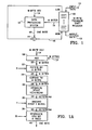
- Figure 1 is a functional block diagram of a block-cipher encryption device according to the present invention.
- Figure 1A is a block diagram of data processing routines performed by the data processing system of Figures 1 and 3.
- Figure 2 is a functional block diagram illustrating details of the discard and segregate functions of the encryption device of Figure 1.
- Figure 3 is a functional block diagram of a block-cipher decryption device according to the present invention.
- a preferred embodiment of a block diagram of a block-cipher encryption device includes an N-bit feedback shift register 10 and a data processing system 12. Except as described below, the data processing system is implemented by firmware in a microprocessor.
- the block-cipher encryption device of Figure 1 processes an N-byte block of plaintext input data 13 with an M-byte encryption key 14 signal to provide an N-byte block of encrypted output data 15.
- the feedback shift register 10 receives an N-byte block of plaintext input data 13.
- the data processing system 12 processes the M most significant bytes 16 of the plaintext input data with the M-byte encryption key 14 by adding the plaintext bytes 16 to the key bytes 14, as illustrated in Figure 1A by a first data processing routine 18.
- this first routine 18 could be something other than addition, such as subtraction or exclusive ORing (XORing), for example.
- the M bytes of data 20 produced by the first routine 18 are then rotated by the data processing system 12 in accordance with a second data processing routine 22 by a number of bytes X in response to a rotation indication X.
- the data processing system 12 then expands the rotated M bytes 26 to provide N bytes of initially processed data 28 by executing a data expansion processing routine 30.
- the Nth byte is produced by XORing the M bytes.
- a pseudorandom nonlinear sequence generator 32 included in the data processing system 12 is initialized by the N bytes of initially processed data 28 and is run to generate a keystream 34.
- the keystream generator 32 is a dynamic-feedback-arrangement-scrambling-technique (DFAST) keystream generator 32, which is implemented in hardware to increase the processing speed of the data processing system 12.
- DFAST keystream generator is described in United States Letters Patent No. 4,860,353 to David S. Brown.
- the preferred embodiment of the DFAST keystream generator 32 includes a dynamic (or nonlinear) feedback shift register and a static (or linear) feedback shift register for receiving input data.
- the DFAST keystream generator 32 provides high speed pseudorandom nonlinear sequence processing of the N bytes 28 to quickly generate a keystream 34 from which a single byte can readily be segregated to create data that can be fedback for processing in subsequent cycles.
- other types of pseudorandom nonlinear sequence generators may be used instead of the DFAST keystream generator 32.
- the data processing system 12 next executes a discard routine 36 and a segregate routine 38 to segregate portions of the keystream 34 into a single byte 40.
- the data processing system 12 segregates the keystream 34 in accordance with the discard routine 36 wherein the beginning of the segregated portion of the keystream 42 is provided at a time related to the beginning of the keystream 34 in response to a duration indication Y by discarding the first Y bytes of the keystream 34.
- the data processing system 12 further segregates the keystream 42 by segregating every nth bit of the keystream 42 from said beginning of said segregated portion in response to a frequency indication n until eight bits are segregated to form the single byte 40.
- the data processing system includes and/or implements a duration indication counter 48 a frequency indication counter 50, a bit counter 52, a byte register 54 and an OR gate 55. All three counters 48, 50, 52 are clocked by the same clock signal 56 as clocks the DFAST keystream generator 32.
- the output of the counter 48 is coupled through the OR gate 55 to the load input of the counter 50.
- the output of the counter 50 is provided to the enable input of the counter 52 and the enable input of the byte register 54 and is also coupled through the OR gate 55 to the input of the counter 50.
- the keystream 32 is provided to the data input of the byte register 54.
- a duration indication Y is loaded into the duration indication counter 48 and a frequency indication n is loaded into the frequency indication counter 50.
- a start pulse 60 is delivered by the duration indication counter 48 to the frequency indication counter 50, which in turn delivers an enable pulse to the bit counter 52 and the byte register 54.
- the byte register is thus enabled to register the concurrent bit of the keystream 34; and the number of bits registered in the byte register 54 is counted by the bit counter 52.
- the frequency indication counter continues to provide a pulse 62 to the enable inputs of the byte register 54 and the bit counter 52 upon every nth count of clock pulses in the DFAST clock signal 56 until the count in the bit counter 52 reaches eight, whereupon a stop pulse 58 is provided to all three counters 48, 50, 52.
- the data processing system 12 further executes a routine 44 by which the single byte 40 formed by segregating portions of the keystream 34 is XOR'd with the least significant byte of data in the feedback shift register 10 to provide a byte of processed data 46.
- This byte of processed data 46 is shifted into the most significant byte position of the feedback shift register 10 and the data in shift register 10 is shifted such that the least significant byte of data is shifted out of the shift register 10.
- the number of cycles to be executed to encrypt a single block of plaintext input data is selected in accordance with the degree of encryption security that is required for the particular application of the encryption device. To ensure that any single bit of the key signal or of the input data can effect every bit of the output data, there should be at least sixteen cycles. Preferably even more cycles are executed to provide still additional security, with the number of cycles being limited by the processing speed of the data processing system 12 in relation to the frequency at which the plaintext input data is provided to the encryption device for encryption.
- the rotation indication X, the duration indication Y and the frequency indication n are separately provided.
- each of these indications may be different in each of the different cycles.
- the selected number of cycles and the rotation indication X, the duration indication Y and the frequency indication n for the respective different cycles are preset in the firmware of the microprocessor.
- the selected number of cycles, and/or the rotation indication X, the duration indication Y and/or the frequency indication n for the respective different cycles are provided as variable inputs to the microprocessor.
- the encrypted output data can be provided by passing the bytes of processed data 46 to a separate component (not shown) apart from the feedback shift register 10.
- FIG. 3 a preferred embodiment of a block diagram of a block-cipher decryption device according to the present invention is identical to the block-cipher encryption device described above with reference to Figures 1 and 2, with the following exceptions.
- the block-cipher decryption device of Figure 3 processes an N-byte block of encrypted input data 13' with an M-byte decryption key 14 signal to provide an N-byte block of decrypted output data 15'.
- the feedback shift register 10 receives an N-byte block of encrypted input data 13'.
- the single byte 40 formed by segregating portions of the keystream 34 is XOR'd with the most significant byte of data in the feedback shift register 10 to provide the byte of processed data 46; and this byte of processed data 46 is shifted into the least significant byte position of the shift register 10, whereby the data in shift register 10 is shifted such that the most significant byte of data is shifted out of the shift register 10.
- the block-cipher decryption device of Figure 3 decrypts encrypted data provided by the block-cipher encryption device of Figure 1 to convert such encrypted data into the plaintext data encrypted by the block-cipher encryption device of Figure 1.
Abstract

Description
- The present invention generally pertains to block-cipher cryptographic devices.
- Block-cipher cryptographic devices based upon the DES (Data Encryption Standard) algorithm are often used when a high degree of encryption security is required. However, at present, encryption/decryption products containing a block-cipher cryptographic device based upon the DES algorithm are restricted from export from the United States of America.
- The present invention provides a block-cipher cryptographic device that is not based upon the DES algorithm but which is compatible therewith and which provides a sufficiently high degree of encryption security for many applications.
- The block-cipher cryptographic device of the present invention is a device that processes plaintext/encrypted input data with a key signal to provide encrypted/decrypted output data. Such device comprises a shift register for receiving input data; and data processing means including a pseudorandom nonlinear sequence generator for executing the following data processing routine a selected number of cycles to provide output data:
processing the contents of said shift register with a key signal to provide initially processed data;
initializing the pseudorandom nonlinear sequence generator with the initially processed data;
running the pseudorandom nonlinear sequence generator to generate a keystream;
segregating portions of the keystream;
processing said segregated portions of said keystream with a portion of the data in the shift register to provide a block of processed data; and
shifting said block of processed data into the shift register. - The degree of security is increased as the selected number of cycles of execution of the data processing routines is increased.
- To further increase the randomness of the pseudorandom keystream generator and hence the security provided by the cryptographic device of the present invention, the data processing routine preferably segregates the keystream in accordance with a routine wherein the beginning of said segregated portion is provided at a time related to the beginning of the keystream in response to a duration indication; segregates every nth bit of the keystream from said beginning of said segregated portion for a selected number of segregated bits in response to a frequency indication; and provides said initially processed data by first processing said shift register contents and said key signal and then rotating data produced by said first processing in response to a rotation indication. The duration indication, the frequency indication and the rotation indication are each separately provided for each of the cycles and may be different for each of the cycles.
- Additional features of the present invention are described in relation to the description of the preferred embodiment.
- Figure 1 is a functional block diagram of a block-cipher encryption device according to the present invention.
- Figure 1A is a block diagram of data processing routines performed by the data processing system of Figures 1 and 3.
- Figure 2 is a functional block diagram illustrating details of the discard and segregate functions of the encryption device of Figure 1.
- Figure 3 is a functional block diagram of a block-cipher decryption device according to the present invention.
- Referring to Figure 1, a preferred embodiment of a block diagram of a block-cipher encryption device according to the present invention includes an N-bit
feedback shift register 10 and adata processing system 12. Except as described below, the data processing system is implemented by firmware in a microprocessor. - The block-cipher encryption device of Figure 1 processes an N-byte block of
plaintext input data 13 with an M-byte encryption key 14 signal to provide an N-byte block ofencrypted output data 15. In a preferred embodiment that is compatible with a DES encryption device, M = 7 and N = 8. - The
feedback shift register 10 receives an N-byte block ofplaintext input data 13. - The
data processing system 12 processes the M mostsignificant bytes 16 of the plaintext input data with the M-byte encryption key 14 by adding theplaintext bytes 16 to thekey bytes 14, as illustrated in Figure 1A by a firstdata processing routine 18. In alternative embodiments thisfirst routine 18 could be something other than addition, such as subtraction or exclusive ORing (XORing), for example. - The M bytes of
data 20 produced by thefirst routine 18 are then rotated by thedata processing system 12 in accordance with a seconddata processing routine 22 by a number of bytes X in response to a rotation indication X. The relationship of the rotatedbytes 26 to the first producedbytes 20 is shown in Table 1 for a rotation indication of three bytes, with M = 7.
- The
data processing system 12 then expands the rotatedM bytes 26 to provide N bytes of initially processeddata 28 by executing a dataexpansion processing routine 30. In the preferred embodiment, wherein M = 7 and N = 8, the Nth byte is produced by XORing the M bytes. - A pseudorandom
nonlinear sequence generator 32, included in thedata processing system 12 is initialized by the N bytes of initially processeddata 28 and is run to generate akeystream 34. In the preferred embodiment thekeystream generator 32 is a dynamic-feedback-arrangement-scrambling-technique (DFAST)keystream generator 32, which is implemented in hardware to increase the processing speed of thedata processing system 12. A DFAST keystream generator is described in United States Letters Patent No. 4,860,353 to David S. Brown. The preferred embodiment of the DFASTkeystream generator 32, as described in said patent, includes a dynamic (or nonlinear) feedback shift register and a static (or linear) feedback shift register for receiving input data. The most significant bytes of theN bytes 28 are received in the dynamic feedback shift register and the remaining bytes are received in the static feedback shift register of the DFASTkeystream generator 32. The DFASTkeystream generator 32 provides high speed pseudorandom nonlinear sequence processing of theN bytes 28 to quickly generate akeystream 34 from which a single byte can readily be segregated to create data that can be fedback for processing in subsequent cycles. In alternative embodiments, other types of pseudorandom nonlinear sequence generators may be used instead of the DFASTkeystream generator 32. - The
data processing system 12 next executes adiscard routine 36 and asegregate routine 38 to segregate portions of thekeystream 34 into asingle byte 40. Thedata processing system 12 segregates thekeystream 34 in accordance with thediscard routine 36 wherein the beginning of the segregated portion of thekeystream 42 is provided at a time related to the beginning of thekeystream 34 in response to a duration indication Y by discarding the first Y bytes of thekeystream 34. - The
data processing system 12 further segregates thekeystream 42 by segregating every nth bit of thekeystream 42 from said beginning of said segregated portion in response to a frequency indication n until eight bits are segregated to form thesingle byte 40. - Details of the
discard routine 36 and thesegregate routine 38 are described with reference to Figure 2. To execute these routines the data processing system includes and/or implements a duration indication counter 48 afrequency indication counter 50, abit counter 52, abyte register 54 and anOR gate 55. All threecounters same clock signal 56 as clocks the DFASTkeystream generator 32. The output of thecounter 48 is coupled through theOR gate 55 to the load input of thecounter 50. The output of thecounter 50 is provided to the enable input of thecounter 52 and the enable input of thebyte register 54 and is also coupled through theOR gate 55 to the input of thecounter 50. Thekeystream 32 is provided to the data input of thebyte register 54. - For each cycle of data processing routines a duration indication Y is loaded into the
duration indication counter 48 and a frequency indication n is loaded into thefrequency indication counter 50. After the first Y bytes of thekeystream 34, astart pulse 60 is delivered by theduration indication counter 48 to thefrequency indication counter 50, which in turn delivers an enable pulse to thebit counter 52 and thebyte register 54. The byte register is thus enabled to register the concurrent bit of thekeystream 34; and the number of bits registered in thebyte register 54 is counted by thebit counter 52. The frequency indication counter continues to provide apulse 62 to the enable inputs of thebyte register 54 and thebit counter 52 upon every nth count of clock pulses in theDFAST clock signal 56 until the count in thebit counter 52 reaches eight, whereupon astop pulse 58 is provided to all threecounters - Referring again to block-cipher encryption device of Figure 1, the
data processing system 12 further executes aroutine 44 by which thesingle byte 40 formed by segregating portions of thekeystream 34 is XOR'd with the least significant byte of data in thefeedback shift register 10 to provide a byte of processeddata 46. - This byte of processed
data 46 is shifted into the most significant byte position of thefeedback shift register 10 and the data inshift register 10 is shifted such that the least significant byte of data is shifted out of theshift register 10. - This completes one cycle of the data processing routines. The number of cycles to be executed to encrypt a single block of plaintext input data is selected in accordance with the degree of encryption security that is required for the particular application of the encryption device. To ensure that any single bit of the key signal or of the input data can effect every bit of the output data, there should be at least sixteen cycles. Preferably even more cycles are executed to provide still additional security, with the number of cycles being limited by the processing speed of the
data processing system 12 in relation to the frequency at which the plaintext input data is provided to the encryption device for encryption. - For each cycle of data processing routines, the rotation indication X, the duration indication Y and the frequency indication n are separately provided. Thus, each of these indications may be different in each of the different cycles.
- In the preferred embodiment the selected number of cycles and the rotation indication X, the duration indication Y and the frequency indication n for the respective different cycles are preset in the firmware of the microprocessor. In alternative embodiments, the selected number of cycles, and/or the rotation indication X, the duration indication Y and/or the frequency indication n for the respective different cycles are provided as variable inputs to the microprocessor.
- After completing the selected number of cycles of processing the
encrypted output data 15 is provided from thefeedback shift register 10. - In alternative embodiments, the encrypted output data can be provided by passing the bytes of processed
data 46 to a separate component (not shown) apart from thefeedback shift register 10. - Referring to Figure 3, a preferred embodiment of a block diagram of a block-cipher decryption device according to the present invention is identical to the block-cipher encryption device described above with reference to Figures 1 and 2, with the following exceptions.
- The block-cipher decryption device of Figure 3 processes an N-byte block of encrypted input data 13' with an M-
byte decryption key 14 signal to provide an N-byte block of decrypted output data 15'. - The
feedback shift register 10 receives an N-byte block of encrypted input data 13'. - In the
data processing routine 44 thesingle byte 40 formed by segregating portions of thekeystream 34 is XOR'd with the most significant byte of data in thefeedback shift register 10 to provide the byte of processeddata 46; and this byte of processeddata 46 is shifted into the least significant byte position of theshift register 10, whereby the data inshift register 10 is shifted such that the most significant byte of data is shifted out of theshift register 10. - The block-cipher decryption device of Figure 3 decrypts encrypted data provided by the block-cipher encryption device of Figure 1 to convert such encrypted data into the plaintext data encrypted by the block-cipher encryption device of Figure 1.
Claims (7)
- A block-cipher cryptographic device for processing plaintext or encrypted input data with a key signal to provide encrypted or decrypted output data respectively, comprising
a shift register (10) for receiving the input data (13); and
data processing means (12), including a pseudorandom nonlinear sequence generator (32), for executing a data processing routine for a selected number of cycles to provide the output data (15), wherein the data processing routine includes:
processing (18, 22, 30) the contents (16) of said shift register with a key signal (14) to provide initially processed data (28);
initializing the pseudorandom nonlinear sequence generator with the initially processed data;
running the pseudorandom nonlinear sequence generator to generate a keystream (34);
segregating (36, 38) portions of the keystream;
processing (44) said segregated portions of said keystream with a portion of the data in the shift register to provide a block of processed data (46); and
shifting said block of processed data into the shift register. - A device according to Claim 1, wherein the data processing means provide said output data in the shift register by said shifting of said blocks of processed data into the shift register for said selected number of cycles.
- A device according to Claim 1, wherein the data processing routine includes segregating (36) a portion of said keystream in accordance with a routine that begins said segregated portion at a time indicated by a duration indication (Y) that is separately provided for each of the cycles and may be different for each of the cycles.
- A device according to Claim 3, wherein the routine for segregating said portion of said keystream includes providing said segregated portion by segregating (38) every nth bit of the keystream from said beginning of said segregated portion for a selected number of segregated bits in response to a frequency indication (n) that is separately provided for each of the cycles and may be different for each of the cycles.
- A device according to Claim 1, wherein the data processing routine includes segregating a portion of said keystream by segregating (38) every nth bit of the keystream from a beginning of said segregated portion for a selected number of segregated bits in response to a frequency indication (n) that is separately provided for each of the cycles and may be different for each of the cycles.
- A device according to any of Claims 1, 3 or 5, wherein the data processing routine includes providing said initially processed data by first processing (18) said shift register contents and said key signal and then rotating (22) data produced by said first processing in response to a rotation indication (X) that is separately provided for each of the cycles and may be different for each of the cycles.
- A device according to any of Claims 1, 3, 4, 5 or 6, wherein the data processing means includes a dynamic-feedback-arrangement-scrambling-technique keystream generator (32) for generating said keystream.
Applications Claiming Priority (2)
| Application Number | Priority Date | Filing Date | Title |
|---|---|---|---|
| US482644 | 1990-02-21 | ||
| US07/482,644 US5054067A (en) | 1990-02-21 | 1990-02-21 | Block-cipher cryptographic device based upon a pseudorandom nonlinear sequence generator |
Publications (3)
| Publication Number | Publication Date |
|---|---|
| EP0443752A2 true EP0443752A2 (en) | 1991-08-28 |
| EP0443752A3 EP0443752A3 (en) | 1992-10-21 |
| EP0443752B1 EP0443752B1 (en) | 1995-11-08 |
Family
ID=23916864
Family Applications (1)
| Application Number | Title | Priority Date | Filing Date |
|---|---|---|---|
| EP91300986A Expired - Lifetime EP0443752B1 (en) | 1990-02-21 | 1991-02-06 | Block-cipher cryptographic device based upon a pseudorandom nonlinear sequence generator |
Country Status (10)
| Country | Link |
|---|---|
| US (1) | US5054067A (en) |
| EP (1) | EP0443752B1 (en) |
| JP (1) | JP3566311B2 (en) |
| KR (1) | KR0175663B1 (en) |
| AT (1) | ATE130144T1 (en) |
| AU (1) | AU634857B2 (en) |
| CA (1) | CA2036489C (en) |
| DE (1) | DE69114324T2 (en) |
| IE (1) | IE69271B1 (en) |
| NO (1) | NO303257B1 (en) |
Cited By (7)
| Publication number | Priority date | Publication date | Assignee | Title |
|---|---|---|---|---|
| GB2306860A (en) * | 1995-10-24 | 1997-05-07 | Motorola Inc | Encryption/decryption system encrypts data using encrypted key |
| ES2123443A1 (en) * | 1996-12-27 | 1999-01-01 | Consejo Superior Investigacion | Method and device for encrypting in data blocks |
| EP1063811A1 (en) * | 1999-06-22 | 2000-12-27 | Hitachi Europe Limited | Cryptographic apparatus and method |
| EP1150468A1 (en) * | 2000-04-26 | 2001-10-31 | Alcatel | Method to generate a pseudo-random sequence of multi-carrier data symbols, and related transmitter and receiver |
| EP1202488A2 (en) * | 2000-10-31 | 2002-05-02 | Sharp Kabushiki Kaisha | Encryption sub-key generation circuit |
| DE102006030325B4 (en) * | 2006-06-30 | 2009-12-31 | Gerhard Kosel | Method for constructing a keystream generator for generating pseudo-random numbers for cryptographic applications |
| EP1835739B1 (en) * | 1999-08-29 | 2018-07-04 | Intel Corporation | Digital video content transmission ciphering and deciphering method and apparatus |
Families Citing this family (60)
| Publication number | Priority date | Publication date | Assignee | Title |
|---|---|---|---|---|
| GB9205291D0 (en) * | 1992-03-11 | 1992-04-22 | Soundcraft Electronics Ltd | Improvements in or relating to the digital control of analogue systems |
| US5365588A (en) * | 1993-03-12 | 1994-11-15 | Hughes Aircraft Company | High speed encryption system and method |
| US5297207A (en) * | 1993-05-24 | 1994-03-22 | Degele Steven T | Machine generation of cryptographic keys by non-linear processes similar to processes normally associated with encryption of data |
| US5377270A (en) * | 1993-06-30 | 1994-12-27 | United Technologies Automotive, Inc. | Cryptographic authentication of transmitted messages using pseudorandom numbers |
| US5363448A (en) * | 1993-06-30 | 1994-11-08 | United Technologies Automotive, Inc. | Pseudorandom number generation and cryptographic authentication |
| US5680131A (en) * | 1993-10-29 | 1997-10-21 | National Semiconductor Corporation | Security system having randomized synchronization code after power up |
| ATE189570T1 (en) * | 1994-02-24 | 2000-02-15 | Merdan Group Inc | METHOD AND DEVICE FOR ESTABLISHING A CRYPTOGRAPHIC CONNECTION BETWEEN ELEMENTS OF A SYSTEM |
| US5787172A (en) * | 1994-02-24 | 1998-07-28 | The Merdan Group, Inc. | Apparatus and method for establishing a cryptographic link between elements of a system |
| US6014446A (en) * | 1995-02-24 | 2000-01-11 | Motorola, Inc. | Apparatus for providing improved encryption protection in a communication system |
| US5724428A (en) * | 1995-11-01 | 1998-03-03 | Rsa Data Security, Inc. | Block encryption algorithm with data-dependent rotations |
| US5949884A (en) * | 1996-11-07 | 1999-09-07 | Entrust Technologies, Ltd. | Design principles of the shade cipher |
| US6049608A (en) * | 1996-12-31 | 2000-04-11 | University Technology Corporation | Variable length nonlinear feedback shift registers with dynamically allocated taps |
| US6182216B1 (en) | 1997-09-17 | 2001-01-30 | Frank C. Luyster | Block cipher method |
| US6215876B1 (en) | 1997-12-31 | 2001-04-10 | Transcrypt International, Inc. | Apparatus for and method of detecting initialization vector errors and maintaining cryptographic synchronization without substantial increase in overhead |
| US6249582B1 (en) | 1997-12-31 | 2001-06-19 | Transcrypt International, Inc. | Apparatus for and method of overhead reduction in a block cipher |
| US6108421A (en) * | 1998-03-06 | 2000-08-22 | Harris Corporation | Method and apparatus for data encryption |
| US6269163B1 (en) | 1998-06-15 | 2001-07-31 | Rsa Security Inc. | Enhanced block ciphers with data-dependent rotations |
| US6490353B1 (en) | 1998-11-23 | 2002-12-03 | Tan Daniel Tiong Hok | Data encrypting and decrypting apparatus and method |
| KR20000066231A (en) * | 1999-04-14 | 2000-11-15 | 유춘열 | Variable Encryption System depending upon timing points and geographical points |
| US6304657B1 (en) * | 1999-05-26 | 2001-10-16 | Matsushita Electric Industrial Co., Ltd. | Data encryption apparatus using odd number of shift-rotations and method |
| US7058817B1 (en) | 1999-07-02 | 2006-06-06 | The Chase Manhattan Bank | System and method for single sign on process for websites with multiple applications and services |
| NL1012581C2 (en) * | 1999-07-13 | 2001-01-16 | Koninkl Kpn Nv | Method of protecting a portable card. |
| JP3724399B2 (en) * | 2001-01-23 | 2005-12-07 | 株式会社日立製作所 | Pseudorandom number generator or encryption / decryption processing device using the same |
| US8849716B1 (en) | 2001-04-20 | 2014-09-30 | Jpmorgan Chase Bank, N.A. | System and method for preventing identity theft or misuse by restricting access |
| AU2002312381A1 (en) | 2001-06-07 | 2002-12-16 | First Usa Bank, N.A. | System and method for rapid updating of credit information |
| KR100403820B1 (en) * | 2001-07-03 | 2003-10-30 | 삼성에스디에스 주식회사 | Apparatus for encrypting plane data and method thereof |
| US7266839B2 (en) | 2001-07-12 | 2007-09-04 | J P Morgan Chase Bank | System and method for providing discriminated content to network users |
| GB2379587B (en) * | 2001-09-10 | 2003-08-20 | Simon Alan Spacey | A method and apparatus for securing electronic information |
| US7987501B2 (en) | 2001-12-04 | 2011-07-26 | Jpmorgan Chase Bank, N.A. | System and method for single session sign-on |
| KR20030067934A (en) * | 2002-02-09 | 2003-08-19 | 공형윤 | Security system of wireless network using random connection node convolutional technique |
| US20180165441A1 (en) | 2002-03-25 | 2018-06-14 | Glenn Cobourn Everhart | Systems and methods for multifactor authentication |
| US8301493B2 (en) | 2002-11-05 | 2012-10-30 | Jpmorgan Chase Bank, N.A. | System and method for providing incentives to consumers to share information |
| US6862446B2 (en) * | 2003-01-31 | 2005-03-01 | Flarion Technologies, Inc. | Methods and apparatus for the utilization of core based nodes for state transfer |
| US7257225B2 (en) * | 2003-12-29 | 2007-08-14 | American Express Travel Related Services Company, Inc. | System and method for high speed reversible data encryption |
| US7620179B2 (en) | 2004-01-29 | 2009-11-17 | Comcast Cable Holdings, Llc | System and method for security processing media streams |
| US20060031873A1 (en) * | 2004-08-09 | 2006-02-09 | Comcast Cable Holdings, Llc | System and method for reduced hierarchy key management |
| WO2006034548A1 (en) * | 2004-09-30 | 2006-04-06 | Synaptic Laboratories Limited | Method of and apparatus for partitioning of a bitstream |
| US8099369B2 (en) * | 2004-12-08 | 2012-01-17 | Ngna, Llc | Method and system for securing content in media systems |
| KR100675837B1 (en) * | 2004-12-13 | 2007-01-29 | 한국전자통신연구원 | Fast-GCM-AES block encoding apparatus and method |
| US7383438B2 (en) * | 2004-12-18 | 2008-06-03 | Comcast Cable Holdings, Llc | System and method for secure conditional access download and reconfiguration |
| US7933410B2 (en) * | 2005-02-16 | 2011-04-26 | Comcast Cable Holdings, Llc | System and method for a variable key ladder |
| US7934083B2 (en) * | 2007-09-14 | 2011-04-26 | Kevin Norman Taylor | Configurable access kernel |
| US8712040B2 (en) * | 2010-01-22 | 2014-04-29 | Harlan J. Brothers | Data-conditioned encryption method |
| US9590959B2 (en) | 2013-02-12 | 2017-03-07 | Amazon Technologies, Inc. | Data security service |
| US10075471B2 (en) | 2012-06-07 | 2018-09-11 | Amazon Technologies, Inc. | Data loss prevention techniques |
| US10084818B1 (en) | 2012-06-07 | 2018-09-25 | Amazon Technologies, Inc. | Flexibly configurable data modification services |
| US9286491B2 (en) | 2012-06-07 | 2016-03-15 | Amazon Technologies, Inc. | Virtual service provider zones |
| US10467422B1 (en) | 2013-02-12 | 2019-11-05 | Amazon Technologies, Inc. | Automatic key rotation |
| US9367697B1 (en) | 2013-02-12 | 2016-06-14 | Amazon Technologies, Inc. | Data security with a security module |
| US10211977B1 (en) | 2013-02-12 | 2019-02-19 | Amazon Technologies, Inc. | Secure management of information using a security module |
| US9300464B1 (en) * | 2013-02-12 | 2016-03-29 | Amazon Technologies, Inc. | Probabilistic key rotation |
| US9705674B2 (en) | 2013-02-12 | 2017-07-11 | Amazon Technologies, Inc. | Federated key management |
| US9608813B1 (en) | 2013-06-13 | 2017-03-28 | Amazon Technologies, Inc. | Key rotation techniques |
| US10210341B2 (en) | 2013-02-12 | 2019-02-19 | Amazon Technologies, Inc. | Delayed data access |
| US9397835B1 (en) | 2014-05-21 | 2016-07-19 | Amazon Technologies, Inc. | Web of trust management in a distributed system |
| US9438421B1 (en) | 2014-06-27 | 2016-09-06 | Amazon Technologies, Inc. | Supporting a fixed transaction rate with a variably-backed logical cryptographic key |
| US9866392B1 (en) | 2014-09-15 | 2018-01-09 | Amazon Technologies, Inc. | Distributed system web of trust provisioning |
| WO2016096000A1 (en) * | 2014-12-17 | 2016-06-23 | Telefonaktiebolaget Lm Ericsson (Publ) | Stream ciphering technique |
| US11115185B2 (en) * | 2019-03-22 | 2021-09-07 | Rosemount Aerospace Inc. | Highly secure WAIC baseband signal transmission with byte displacement approach |
| US11537740B2 (en) | 2021-01-04 | 2022-12-27 | Bank Of America Corporation | System for enhanced data security using versioned encryption |
Citations (2)
| Publication number | Priority date | Publication date | Assignee | Title |
|---|---|---|---|---|
| DE3244537A1 (en) * | 1982-12-02 | 1984-06-07 | Ant Nachrichtentech | Method for encrypting and decrypting data blocks |
| US4860353A (en) * | 1988-05-17 | 1989-08-22 | General Instrument Corporation | Dynamic feedback arrangement scrambling technique keystream generator |
Family Cites Families (4)
| Publication number | Priority date | Publication date | Assignee | Title |
|---|---|---|---|---|
| US4255811A (en) * | 1975-03-25 | 1981-03-10 | International Business Machines Corporation | Key controlled block cipher cryptographic system |
| US4316055A (en) * | 1976-12-30 | 1982-02-16 | International Business Machines Corporation | Stream/block cipher crytographic system |
| US4663500A (en) * | 1982-02-22 | 1987-05-05 | Nec Corporation | Cryptographic system |
| NL8602847A (en) * | 1986-11-11 | 1988-06-01 | Philips Nv | METHOD FOR Ciphering / Deciphering and Device for Carrying Out the Method |
-
1990
- 1990-02-21 US US07/482,644 patent/US5054067A/en not_active Expired - Lifetime
-
1991
- 1991-02-06 AT AT91300986T patent/ATE130144T1/en not_active IP Right Cessation
- 1991-02-06 DE DE69114324T patent/DE69114324T2/en not_active Expired - Fee Related
- 1991-02-06 EP EP91300986A patent/EP0443752B1/en not_active Expired - Lifetime
- 1991-02-07 IE IE40591A patent/IE69271B1/en not_active IP Right Cessation
- 1991-02-13 AU AU71002/91A patent/AU634857B2/en not_active Ceased
- 1991-02-15 CA CA002036489A patent/CA2036489C/en not_active Expired - Fee Related
- 1991-02-19 NO NO910658A patent/NO303257B1/en unknown
- 1991-02-20 KR KR1019910002694A patent/KR0175663B1/en not_active IP Right Cessation
- 1991-02-20 JP JP02638591A patent/JP3566311B2/en not_active Expired - Fee Related
Patent Citations (2)
| Publication number | Priority date | Publication date | Assignee | Title |
|---|---|---|---|---|
| DE3244537A1 (en) * | 1982-12-02 | 1984-06-07 | Ant Nachrichtentech | Method for encrypting and decrypting data blocks |
| US4860353A (en) * | 1988-05-17 | 1989-08-22 | General Instrument Corporation | Dynamic feedback arrangement scrambling technique keystream generator |
Non-Patent Citations (1)
| Title |
|---|
| ELECTRO 77 Conf. Rec. April 1977, Session 30/4, EL SEGUNDO (US) Pages 1-6; JEFFERY ET AL: 'Data Encryption' * |
Cited By (16)
| Publication number | Priority date | Publication date | Assignee | Title |
|---|---|---|---|---|
| GB2306860A (en) * | 1995-10-24 | 1997-05-07 | Motorola Inc | Encryption/decryption system encrypts data using encrypted key |
| ES2123443A1 (en) * | 1996-12-27 | 1999-01-01 | Consejo Superior Investigacion | Method and device for encrypting in data blocks |
| US7177424B1 (en) | 1999-06-22 | 2007-02-13 | Hitachi, Ltd. | Cryptographic apparatus and method |
| EP1063811A1 (en) * | 1999-06-22 | 2000-12-27 | Hitachi Europe Limited | Cryptographic apparatus and method |
| EP1835739B1 (en) * | 1999-08-29 | 2018-07-04 | Intel Corporation | Digital video content transmission ciphering and deciphering method and apparatus |
| KR100764415B1 (en) * | 2000-04-26 | 2007-10-05 | 알까뗄 | Method to generate a pseudo random sequence of multi carrier data symbols, and related transmitter and receiver |
| AU776537B2 (en) * | 2000-04-26 | 2004-09-16 | Alcatel | Method to generate a pseudo-random sequence of multi-carrier data symbols, and related transmitter and receiver |
| EP1599002A1 (en) * | 2000-04-26 | 2005-11-23 | Alcatel | Method to generate a pseudo random sequence of multi carrier data symbols, and related transmitter and receiver |
| US7035408B2 (en) | 2000-04-26 | 2006-04-25 | Alcatel | Method to generate pseudo-random sequence of multi-carrier data symbols, and related transmitter and receiver |
| US7502469B2 (en) | 2000-04-26 | 2009-03-10 | Alcatel | Method to generate a pseudo random sequence of multi carrier data symbols, and related transmitter and receiver |
| EP1150468A1 (en) * | 2000-04-26 | 2001-10-31 | Alcatel | Method to generate a pseudo-random sequence of multi-carrier data symbols, and related transmitter and receiver |
| KR100442913B1 (en) * | 2000-10-31 | 2004-08-02 | 샤프 가부시키가이샤 | Encryption key generation circuit |
| US7039186B2 (en) | 2000-10-31 | 2006-05-02 | Sharp Kabushiki Kaisha | Encryption key generation circuit |
| EP1202488A3 (en) * | 2000-10-31 | 2003-03-19 | Sharp Kabushiki Kaisha | Encryption sub-key generation circuit |
| EP1202488A2 (en) * | 2000-10-31 | 2002-05-02 | Sharp Kabushiki Kaisha | Encryption sub-key generation circuit |
| DE102006030325B4 (en) * | 2006-06-30 | 2009-12-31 | Gerhard Kosel | Method for constructing a keystream generator for generating pseudo-random numbers for cryptographic applications |
Also Published As
| Publication number | Publication date |
|---|---|
| CA2036489C (en) | 2001-04-17 |
| NO910658D0 (en) | 1991-02-19 |
| NO303257B1 (en) | 1998-06-15 |
| IE910405A1 (en) | 1991-08-28 |
| IE69271B1 (en) | 1996-08-21 |
| DE69114324T2 (en) | 1996-06-20 |
| KR0175663B1 (en) | 1999-05-15 |
| EP0443752A3 (en) | 1992-10-21 |
| ATE130144T1 (en) | 1995-11-15 |
| US5054067A (en) | 1991-10-01 |
| JP3566311B2 (en) | 2004-09-15 |
| AU634857B2 (en) | 1993-03-04 |
| DE69114324D1 (en) | 1995-12-14 |
| AU7100291A (en) | 1991-08-22 |
| CA2036489A1 (en) | 1991-08-22 |
| JPH04215689A (en) | 1992-08-06 |
| EP0443752B1 (en) | 1995-11-08 |
| NO910658L (en) | 1991-08-22 |
Similar Documents
| Publication | Publication Date | Title |
|---|---|---|
| EP0443752B1 (en) | Block-cipher cryptographic device based upon a pseudorandom nonlinear sequence generator | |
| EP0467239B1 (en) | An encryption system based on Chaos theory | |
| EP0615361B1 (en) | System and method for high speed encryption using multiple keystream generator | |
| US7280657B2 (en) | Data encryption and decryption system and method using merged ciphers | |
| JP3724399B2 (en) | Pseudorandom number generator or encryption / decryption processing device using the same | |
| JPS5832380B2 (en) | Cryptographic processing equipment | |
| WO2009100104A1 (en) | Cryptographic system incorporating a digitally generated chaotic numerical sequence | |
| AU2005200388A1 (en) | Stream cipher design with revolving buffers | |
| Zelenoritskaya et al. | Possible modifications of RC4 stream cipher | |
| JPS5843743B2 (en) | Encryption method | |
| JPS6281145A (en) | Data ciphering system | |
| Michener | The use of complete, nonlinear, block codes for nonlinear, noninvertible mixing of pseudorandom sequences | |
| RU2007884C1 (en) | Device for encrypting binary information | |
| KR100316025B1 (en) | Encryption and decryption device using data encryption standard algorithm | |
| Svensson et al. | A simple secure communications system utilizing chaotic functions to control the encryption and decryption of messages | |
| JPH03155591A (en) | Sequential ciphering device | |
| Hasan | Key-joined block ciphers with input-output pseudorandom shuffling applied to remotely keyed authenticated encryption | |
| Rubin | Designing a high-security cipher | |
| Rubin | DECRYPTING A STREAM CIPHER BASED ON JK FLIP-FLOPS | |
| BG67431B1 (en) | Method and device for keystream generating for stream ciphers | |
| Guerrero et al. | Customised hardware based on the REDOC III algorithm for high performance data ciphering | |
| JPH081367U (en) | Sequential encryption device | |
| Sun | 6.857 Computer & Network Security Final Project: Differential Fault Analysis | |
| Sun | Differential Fault Analysis | |
| Milleville | Vernam Two |
Legal Events
| Date | Code | Title | Description |
|---|---|---|---|
| PUAI | Public reference made under article 153(3) epc to a published international application that has entered the european phase |
Free format text: ORIGINAL CODE: 0009012 |
|
| AK | Designated contracting states |
Kind code of ref document: A2 Designated state(s): AT BE CH DE DK ES FR GB GR IT LI LU NL SE |
|
| PUAL | Search report despatched |
Free format text: ORIGINAL CODE: 0009013 |
|
| AK | Designated contracting states |
Kind code of ref document: A3 Designated state(s): AT BE CH DE DK ES FR GB GR IT LI LU NL SE |
|
| 17P | Request for examination filed |
Effective date: 19930104 |
|
| 17Q | First examination report despatched |
Effective date: 19940609 |
|
| RAP1 | Party data changed (applicant data changed or rights of an application transferred) |
Owner name: GENERAL INSTRUMENT CORPORATION OF DELAWARE |
|
| GRAA | (expected) grant |
Free format text: ORIGINAL CODE: 0009210 |
|
| AK | Designated contracting states |
Kind code of ref document: B1 Designated state(s): AT BE CH DE DK ES FR GB GR IT LI LU NL SE |
|
| PG25 | Lapsed in a contracting state [announced via postgrant information from national office to epo] |
Ref country code: IT Free format text: LAPSE BECAUSE OF FAILURE TO SUBMIT A TRANSLATION OF THE DESCRIPTION OR TO PAY THE FEE WITHIN THE PRE;WARNING: LAPSES OF ITALIAN PATENTS WITH EFFECTIVE DATE BEFORE 2007 MAY HAVE OCCURRED AT ANY TIME BEFORE 2007. THE CORRECT EFFECTIVE DATE MAY BE DIFFERENT FROM THE ONE RECORDED.SCRIBED TIME-LIMIT Effective date: 19951108 Ref country code: NL Free format text: LAPSE BECAUSE OF FAILURE TO SUBMIT A TRANSLATION OF THE DESCRIPTION OR TO PAY THE FEE WITHIN THE PRESCRIBED TIME-LIMIT Effective date: 19951108 Ref country code: LI Effective date: 19951108 Ref country code: BE Effective date: 19951108 Ref country code: AT Effective date: 19951108 Ref country code: GR Free format text: LAPSE BECAUSE OF FAILURE TO SUBMIT A TRANSLATION OF THE DESCRIPTION OR TO PAY THE FEE WITHIN THE PRESCRIBED TIME-LIMIT Effective date: 19951108 Ref country code: CH Effective date: 19951108 Ref country code: DK Effective date: 19951108 |
|
| REF | Corresponds to: |
Ref document number: 130144 Country of ref document: AT Date of ref document: 19951115 Kind code of ref document: T |
|
| REF | Corresponds to: |
Ref document number: 69114324 Country of ref document: DE Date of ref document: 19951214 |
|
| ET | Fr: translation filed | ||
| PG25 | Lapsed in a contracting state [announced via postgrant information from national office to epo] |
Ref country code: SE Effective date: 19960208 |
|
| PG25 | Lapsed in a contracting state [announced via postgrant information from national office to epo] |
Ref country code: ES Free format text: LAPSE BECAUSE OF FAILURE TO SUBMIT A TRANSLATION OF THE DESCRIPTION OR TO PAY THE FEE WITHIN THE PRESCRIBED TIME-LIMIT Effective date: 19960219 |
|
| PGFP | Annual fee paid to national office [announced via postgrant information from national office to epo] |
Ref country code: SE Payment date: 19960221 Year of fee payment: 6 |
|
| PGFP | Annual fee paid to national office [announced via postgrant information from national office to epo] |
Ref country code: DK Payment date: 19960223 Year of fee payment: 6 |
|
| PGFP | Annual fee paid to national office [announced via postgrant information from national office to epo] |
Ref country code: BE Payment date: 19960226 Year of fee payment: 6 |
|
| PGFP | Annual fee paid to national office [announced via postgrant information from national office to epo] |
Ref country code: CH Payment date: 19960312 Year of fee payment: 6 |
|
| NLV1 | Nl: lapsed or annulled due to failure to fulfill the requirements of art. 29p and 29m of the patents act | ||
| REG | Reference to a national code |
Ref country code: CH Ref legal event code: PL |
|
| PLBE | No opposition filed within time limit |
Free format text: ORIGINAL CODE: 0009261 |
|
| STAA | Information on the status of an ep patent application or granted ep patent |
Free format text: STATUS: NO OPPOSITION FILED WITHIN TIME LIMIT |
|
| 26N | No opposition filed | ||
| PGFP | Annual fee paid to national office [announced via postgrant information from national office to epo] |
Ref country code: ES Payment date: 19970217 Year of fee payment: 7 |
|
| PGFP | Annual fee paid to national office [announced via postgrant information from national office to epo] |
Ref country code: LU Payment date: 19980217 Year of fee payment: 8 |
|
| REG | Reference to a national code |
Ref country code: GB Ref legal event code: 732E |
|
| PG25 | Lapsed in a contracting state [announced via postgrant information from national office to epo] |
Ref country code: LU Free format text: LAPSE BECAUSE OF NON-PAYMENT OF DUE FEES Effective date: 19990206 |
|
| REG | Reference to a national code |
Ref country code: GB Ref legal event code: IF02 |
|
| PGFP | Annual fee paid to national office [announced via postgrant information from national office to epo] |
Ref country code: DE Payment date: 20080229 Year of fee payment: 18 Ref country code: GB Payment date: 20080108 Year of fee payment: 18 |
|
| PGFP | Annual fee paid to national office [announced via postgrant information from national office to epo] |
Ref country code: FR Payment date: 20080212 Year of fee payment: 18 |
|
| GBPC | Gb: european patent ceased through non-payment of renewal fee |
Effective date: 20090206 |
|
| REG | Reference to a national code |
Ref country code: FR Ref legal event code: ST Effective date: 20091030 |
|
| PG25 | Lapsed in a contracting state [announced via postgrant information from national office to epo] |
Ref country code: DE Free format text: LAPSE BECAUSE OF NON-PAYMENT OF DUE FEES Effective date: 20090901 |
|
| PG25 | Lapsed in a contracting state [announced via postgrant information from national office to epo] |
Ref country code: FR Free format text: LAPSE BECAUSE OF NON-PAYMENT OF DUE FEES Effective date: 20090302 Ref country code: GB Free format text: LAPSE BECAUSE OF NON-PAYMENT OF DUE FEES Effective date: 20090206 |
|
| P01 | Opt-out of the competence of the unified patent court (upc) registered |
Effective date: 20230520 |