EP0442498A2 - Accumulation time control apparatus - Google Patents
Accumulation time control apparatus Download PDFInfo
- Publication number
- EP0442498A2 EP0442498A2 EP91102103A EP91102103A EP0442498A2 EP 0442498 A2 EP0442498 A2 EP 0442498A2 EP 91102103 A EP91102103 A EP 91102103A EP 91102103 A EP91102103 A EP 91102103A EP 0442498 A2 EP0442498 A2 EP 0442498A2
- Authority
- EP
- European Patent Office
- Prior art keywords
- accumulation
- sensor
- sensor means
- image pickup
- control
- Prior art date
- Legal status (The legal status is an assumption and is not a legal conclusion. Google has not performed a legal analysis and makes no representation as to the accuracy of the status listed.)
- Granted
Links
Images


Classifications
-
- G—PHYSICS
- G02—OPTICS
- G02B—OPTICAL ELEMENTS, SYSTEMS OR APPARATUS
- G02B7/00—Mountings, adjusting means, or light-tight connections, for optical elements
- G02B7/28—Systems for automatic generation of focusing signals
- G02B7/34—Systems for automatic generation of focusing signals using different areas in a pupil plane
- G02B7/346—Systems for automatic generation of focusing signals using different areas in a pupil plane using horizontal and vertical areas in the pupil plane, i.e. wide area autofocusing
-
- C—CHEMISTRY; METALLURGY
- C08—ORGANIC MACROMOLECULAR COMPOUNDS; THEIR PREPARATION OR CHEMICAL WORKING-UP; COMPOSITIONS BASED THEREON
- C08F—MACROMOLECULAR COMPOUNDS OBTAINED BY REACTIONS ONLY INVOLVING CARBON-TO-CARBON UNSATURATED BONDS
- C08F210/00—Copolymers of unsaturated aliphatic hydrocarbons having only one carbon-to-carbon double bond
- C08F210/04—Monomers containing three or four carbon atoms
- C08F210/06—Propene
-
- C—CHEMISTRY; METALLURGY
- C08—ORGANIC MACROMOLECULAR COMPOUNDS; THEIR PREPARATION OR CHEMICAL WORKING-UP; COMPOSITIONS BASED THEREON
- C08F—MACROMOLECULAR COMPOUNDS OBTAINED BY REACTIONS ONLY INVOLVING CARBON-TO-CARBON UNSATURATED BONDS
- C08F210/00—Copolymers of unsaturated aliphatic hydrocarbons having only one carbon-to-carbon double bond
- C08F210/04—Monomers containing three or four carbon atoms
- C08F210/08—Butenes
Definitions
- the present invention relates to an accumulation time control apparatus of sensors which are used in a focal point detecting apparatus having a plurality of distance measuring visual fields or the like.
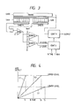
- Fig. 1 shows an AF optical system of the typical double image phase difference detecting type.
- a field lens FLD having the same optical axis as that of a photographing lens LNS whose focal point is to be detected is arranged.
- Two secondary image forming lenses FCLA and FCLB are arranged at positions which are symmetrical with respect to an optical axis behind the field lens FLD.
- Sensor trains SAA and SAB are arranged at positions further behind the lenses FCLA and FCLB.
- Diaphragms DIA and DIB are arranged near the secondary image forming lenses FCLA and FCLB.
- the field lens FLD forms an image of an exit pupil of the photographing lens LNS almost onto pupil surfaces of the two secondary image forming lenses FCLA and FCLB.
- the light fluxes which respectively enter the secondary image forming lenses FCLA and FCLB are light fluxes which were emitted from the regions having the same area which are not mutually overlapped and correspond to the secondary image forming lenses FCLA and FCLB on the exit pupel surface of the photographing lens LNS.
- Fig. 2 shows an example of photoelectric conversion outputs of two images formed on the sensor trains SAA and SAB.
- the output of the SAA assumes A(i) and the output of the SAB assumes B(i).
- the photographing lens can be set into an in-focus state by adjusting a focal point of the photographing lens on the basis of the image deviation amount obtained by the methods disclosed in those Official Gazettes.
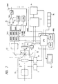
- control sensors SAGCA and SAGCB are arranged at positions adjacent to the sensor arrays SAA and SAB and observe almost the same object portion as the distance measuring visual field images. Outputs of the control sensors SAGCA and SAGCB are added by an adder ADD and an addition signal is supplied from the adder ADD to comparators COMP1 and COMP2.
- a referred potential which is compared with the addition output by each comparator is obtained by dividing a reference potential V ref .
- the referred potentials correspond respectively to the upper level and lower level in Fig. 4.
- Output signals of the comparators are always supplied to a control circuit CONT2 and are referred at a necessary time point.
- a control signal to control a control circuit CONT1 is generated from the control circuit CONT2.
- the control circuit CONT1 receives the control signal from the control circuit CONT2 and transfers and reads out the photo charges of the AF sensors to a transfer channel TRANS through a gate GATE in order to terminate the accumulation of the charges by the AF sensors.
- the read-out charges are supplied to an operating circuit through an amplifier of a designated gain.
- the control circuit CONT2 receives two kinds of time designation pulses BTIME and TMAX and executes the following operation.
- the accumulation is finished at that time point and a signal is generated so as to select an amplifier of a low gain in the control circuit CONT1.
- the output signal of the adder ADD changes in accordance with a straight line L1 in Fig 4 with the elapse of the accumulation time and the accumulation is finished at time T1 before the time point of the pulse BTIME.
- the gain of the amplifier in the control circuit CONT1 is selected in response to the pulse BTIME. That is, if the accumulation amount of the control sensor is higher than the lower level at that time point, the low gain is selected and the accumulation is continued until the accumulation amount is equal to the upper level of the comparator.
- the output of the adder ADD changes in accordance with the straight line L2 in Fig. 4.
- the accumulation is finished at time T2.
- the control circuit CONT2 instructs the control circuit CONT1 to use an amplifier of a high gain.
- a ratio of two gains is set to a value which is equal to a ratio of two comparison levels.
- the AF light fluxes are transmitted via mirror reflecting members M1 and M2 to extend a length of optical path and enter a pair of image reforming lenses FCLA and FCLB and images are again formed onto the surfaces of the sensors.
- Three pairs of sensor arrays that is, a pair of sensor arrays SAA1 and SAB1, a pair of sensor arrays SAA2 and SAB2, and a pair of sensor arrays SAA3 and SAB3 are used to individually receive the reformed optical images which reached from three visual fields of the visual field mask VMSK.
- a method of controlling the sensors is the same as that in the conventional apparatus.
- the accumulating operations of all of the sensor pairs are started in a lump and the accumulation control as mentioned above is executed for each sensor pair.
- the above method is based on the idea such that the main object exists at the nearest position and the images existing at relatively remote positions other than the main object are the background.
- a device of weighting in a manner such that the selection algorithm of the distance measuring points is changed in accordance with a focal point distance of the photographing lens and on the side of a short focal point, the selection of the central visual field is made easy or the like.
- the method of controlling the accumulation of the sensors as mentioned above generally, in the case where there is a luminance difference in the picture plane of an object, the sensor output of the distance measuring point at which a portion of a low luminance is seen does not reach a predetermined level, so that the accumulation is not finished, a desired time of the AF operation becomes remarkably long, and the operability of the apparatus is lost.
- a contrast constant control method has been known as a method of controlling the accumulation time.
- contrasts of the light intensity distributions on the AF sensors differ depending on a pattern of an object, so that the accumulation times of the sensors having different distance measuring visual field differ.
- the sensor which observes a wall or a cloth of a solid color even if the accumulating operation was executed for a long time, a contrast enough to reach a comparison level is not obtained. Therefore, even in a bright state, the maximum limit accumulating operation is soon performed.
- the invention is made in consideration of the above circumstances and it is an object of the invention to improve a response speed of an apparatus for controlling accumulation times for a plurality of sensor means.
- an accumulation time control apparatus comprising a plurality of sensor means and control means for respectively controlling charge accumulation times in the sensor means, wherein on the basis of the accumulation time in either one of the sensor means whose accumulation amount has first reached a predetermined level, the control means sets the accumulation times of the other sensor means, and wherein each of the plurality of sensor means has a long photo sensitive surface which is extended in a predetermined direction for each distance measuring visual field and at least one of the sensor means has a photo sensitive surface which is extended in a direction different from the above predetermined direction.
- the whole accumulation time can be determined by the time which was required to first complete the accumulation. Therefore, for example, in the case of applying the invention to an AF apparatus, even in the case where either one of the distance measuring visual fields has extremely lower luminance and contrast than those of the other distance measuring visual fields, the delay of the AF operation by such a distance measuring visual field can be prevented. A response speed of such a kind of apparatus can be remarkably improved.
- the photo sensitive surface of at least one of the sensor means includes a photo sensitive surface which extends in a direction different from the photo sensitive surfaces of the other sensor means, so that a dependency of the photo sensitive surface of the sensor means on the pattern can be reduced.
- Fig. 7 is a block diagram showing a construction of an electronic still camera according to an embodiment.
- an image pickup light from an object which was supplied through an image pickup optical system 1 is photoelectrically converted by an image pickup device 2 using a CCD or the like.
- An electric video signal obtained by the photoelectric conversion is processed by a signal processing circuit 3. After that, the video signal is recorded onto a recording medium such as a magnetic disk or the like by a recording section 4.
- the image pickup optical system 1 has an iris 5 and a focusing lens 6.
- the iris 5 is driven by an iris driving circuit 7.
- the focusing lens 6 is driven by a focusing driving circuit 8.
- the image pickup lights which were reflected by mirrors 9 and 10 arranged on an optical axis of the image pickup optical system 1 are led to an AF optical system 11 and a photometric optical system 12, respectively.
- the image pickup light which was led to the AF optical system 11 is illuminated onto an AF sensor SAS through various optical devices as shown in Fig. 6.
- the image pickup light which was led to the photometric optical system 12 is illuminated onto a photometric sensor 13.
- the electronic still camera has: a control circuit CONT to control the AF sensor SAS; and a microprocessor PRS to control the control circuit CONT, AF sensor SAS, and the like.
- a CPU which constructs the microprocessor PRS controls the signal processing circuit 3 and the recording section 4 in accordance with the operations of various operation switches 14. Further, the CPU supplies an iris control signal according to a photometric output of the photometric sensor 13 to the iris driving circuit 7. The CPU also supplies a focusing control signal according to an output of the AF sensor SAS which is supplied through the control circuit CONT to the focusing driving circuit 8.
- An operating mode and the like of the camera are displayed by a display device 15 using a liquid crystal or the like.
- the microprocessor PRS comprises a CPU, a ROM, and a RAM.
- the CPU properly reads out and executes various program data stored in the ROM in accordance with the operations of the switches and controls the writing and reading operations of the various data which are supplied in association with the execution of the prgram into and from the RAM.
- the AF sensor SAS has three pairs of sensors.
- the AF light fluxes are irradiated to a pair of sensors SAA1 and SAB1, a pair of sensors SAA2 and SAB2, and a pair of sensors SAA3 and SAB3 through the field lenses FLD1 to FLD3 and the visual field mask VMSK of the AF image pickup system shown in Fig. 6.
- Outputs of the sensors are used as control outputs.
- the control outputs can be also derived from control sensors.
- the control circuit CONT comprises: analog amplifiers A1 and A2 to amplify the output of the sensor SAS by different predetermined gains, respectively; a switching circuit SW to selectively supply outputs of the analog amplifiers to an A/D converter; a gain control circuit G.CONT to substantially switch the gains for the outputs of the analog amplifiers by switching and controlling the switching circuit SW in accordance with an output level of the sensor SAS; and a timing control circuit T.CONT to control the timings to start or stop the accumulation of the sensor SAS.
- control circuit CONT and the microprocessor in the embodiment can be also obviously constructed by a one-chip microcomputer.
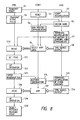
- Fig. 8 is a flowchart showing the operation of the first embodiment of the invention. The operation will now be described hereinbelow.
- the microprocessor PRS sends an accumulation start signal START to the AF sensor through a data communication path FTIME regarding the timings at the start of the AF sequence after the iris was adjusted (step S1), thereby starting the accumulation of the sensor SAS (step S2).
- the microprocessor PRS also resets the control circuit CONT into the initial state (step S3).
- the microprocessor PRS supplies a pulse BTIME to the sensor through the line FTIME for a gain decision time in accordance with the content of the program (step S4).
- each of the three sensor array pairs in the sensor SAS determines an accumulation termination level to either the upper level or the lower level on the basis of the foregoing method of Fig. 4 (step S5).
- the accumulation termination level (corresponding to the selected amplifier gain upon reading) of each sensor array pair is supplied through a line GAIN to the gain control circuit G.CONT and stored (step S6).
- the sensor SAS communicates an ID signal of such a pair of sensor array whose accumulation was finished to the microprocessor PRS and the control circuit CONT through a line SLINE (step S7).
- the sensor SAS also time sequentially generates an image signal from a terminal SOUT in response to a clock signal (not shown) (step S8). Further, a proper one of the gains of the analog amplifiers A1 and A2 having different predetermined gains is selected on the basis of the designated gain stored in the gain control circuit G.CONT (step S9).
- the output of the sensor SAS is amplified and A/D converted and sent as digital data to the microprocessor PRS.
- the microprocessor PRS reads a signal on the line SLINE before one AF focal point of the distance measuring visual field is calculated from the output signals of the sensor array pair SAA1 and SAB1 (step S10).
- one AF focal point of the distance measuring visual field is calculated on the basis of the output signals of the sensor array pair SAA1 and SAB1 (step S12). After that, the calculated AF focal point is stored.
- step S13 When the timer interruption is generated by the program timer (step S13), a program to forcedly terminate the accumulating operation of the other sensor array which is executing the accumulation even if a charge accumulation amount of such a sensor array doesn't reach the accumulation end level is activated (step S14).
- a forced end signal is sent to the line FTIME.
- the timing control circuit TCONT Upon reception of the forced end signal, the timing control circuit TCONT sends an accumulation end control signal TINT to the sensor SAS, thereby finishing the accumulating operation (step S15).
- step S20 If the accumulation level of the other line of the sensor array has reached a predetermined end level for a period of time between TINT1 and T end , the termination of the accumulation, the signal transmission, the calculation of the AF focal point, and the like are executed in accordance with the ordinary control sequence (steps S16 to S19). After that, the optimum distance measuring point is selected from the AF operation outputs (step S20).
- the AF operation output at the distance measuring point is supplied to the AF circuit and the AF lens is moved.
- the accumulation of the sensor array which is executing the accumulating operation is finished by the above requirement.
- the operating times of the sensors in the case where the luminance differences among the distance measuring points are large and there is a remarkably large variation among the accumulation times in the conventional method can be suppressed to a constant time (T end ).
- T end a constant time
- a magnification coefficient K is properly set to a value within a range of 1 ⁇ K ⁇ 8, preferably, 1 ⁇ K ⁇ 4. If the value of K is too large, an effect to reduce the accumulation time is not obtained. If it is too small, there is a tendency such that a priority is eventually given to a high luminance and a high contrast.
- the accumulating operations of the other sensor arrays are finished at the time which is K times as long as the accumulation time TINT1 of the sensor array whose accumulating operation was first finished.
- the accumulation is finished before charges are accumulated into the other sensor array in a visual field which is seeing a main object until a meaning signal level. Therefore, only when the input signal is a signal having a high reliability in which an in-focus state can be detected as a result of the discrimination, the accumulation time of such a sensor array is used as TINT1 in the above equation (1). If a sufficient high speed microcomputer is used, the control delay time can be ignored because a time which is required for the operation and discrimination is short.
- the set lower limit value is set to a value within a range from 20 to 200 msec, preferably, about 40 to 160 msec. Since the accumulating operations of a few times are required until the photographing lens is set to an in-focus state, if the above lower limit value is set to a long time, the effect of the invention decreases.
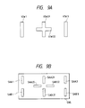
- Fig. 9A shows an arrangement of a distance measuring visual field of the AF system of the embodiment. That is, a lateral visual field VIW22 of a distance measuring visual field of the central portion is added to the foregoing embodiment.
- the lateral visual field VIW22 is used to improve a dependency on a pattern. If only a visual field in the vertical direction is used, the AF system cannot respond to a pattern such as a vertical line. Therefore, the lateral visual field VIW22 which crosses perpendicularly to a visual field VIW21 in the vertical direction is provided, thereby eliminating a merit and a demerit of an object depending on the direction of a pattern.
- an optical method of perpendicularly arranging the central visual fields VIW21 and VIW22 can be realized by arranging four image reforming lenses in a crossing (+) shape. It is sufficient to also provide two AF systems in each of which a pair of two image reforming lenses are provided and which have hitherto frequently been used. With the above construction, a sensor arrangement shown in Fig. 9B is derived.
- a sensor array pair SAA1 and SAB1 are arranged in correspondence to a distance measuring visual field VIW1
- a sensor array pair SAA21 and SAB21 are arranged in correspondence to the distance measuring visual field VIW21
- a sensor array pair SAA22 and SAB22 are arranged in correspondence to the distance measuring visual field VIW22
- a sensor array pair SAA3 and SAB3 are arranged in correspondence to a distance measuring visual field VIW3 , respectively.
- the accumulation times of the above four pairs of sensor arrays are controlled in the following manner.
- the value of K in the equation (1) is set to a small value within a range from 1 to 4, preferably, from 1 to 2, thereby controlling the accumulation.
- K is set to a value within a range from 1 to 8, preferably, from 2 to 4 in the equation (1) in a manner similar to that in the foregoing embodiment.
- the visual field which earlier finishes the accumulation has information suitable for the AF operation. Since such information relates to the same position of the object, it is advantageous for the system to also finish the accumulation of the array in the other perpendicular direction as quickly as possible in accordance with the operation of the AF sensor array of the better visual field which first finishes the accumulation.
- the value of K in the equation (1) is changed and applied between the two central visual fields VIW21 and VIW22 and among three points of the left, right, and center positions, and it is desirable to use a small value in the case of between the two central visual fields and to use a relatively large value similarly to the foregoing embodiment in the case among the three left, right, and center points.
- the accumulation is forcedly finished among the three right, left, and center points, if the sensor array which sees either one of the vertical and lateral visual fields in the central portion first finished the accumulation, the accumulating operations of the right and left sensors are limited on the basis of the accumulation time of such a sensor array which first finished the accumulation.
- the accumulating operations to the two central visual fields are simultaneously limited in the vertical and lateral directions.
- the accumulation times of the other sensors can be also obviously controlled by the AF detection.
- the invention can be also applied to an AF apparatus which is constructed by extracting only the systems of two visual fields in the central, vertical, and lateral directions in the embodiment.
- the invention is not always limited to two visual fields which cross perpendicularly.
- the above method is effective in a visual field construction such as to substantially scan the same position of an object in different directions.
- the invention has been applied to a multipoint AF apparatus.
- the invention can be also obviously applied to the control of the accumulation time of each sensor output of a multiplate type camera.
- the operating speed of the AF apparatus having a plurality of distance measuring visual fields can be remarkably improved and the operation feeling of various apparatuses such as camera and the like can be improved.
- An accumulation time control apparatus comprises a plurality of sensors and a control circuit to control charge accumulation times of the sensors, respectively, wherein on the basis of the accumulation time in either one of the sensors whose accumulation amount has first reached a predetermined level, the control circuit sets the accumulation times of the other sensors.
Abstract
Description
- The present invention relates to an accumulation time control apparatus of sensors which are used in a focal point detecting apparatus having a plurality of distance measuring visual fields or the like.
- Hitherto, various methods of controlling an accumulation time of an AF sensor have been proposed. However, in most of the cases, there is generally used a method comprising a combination of both of a control method of terminating the accumulating operation when a charge accumulation amount has reached a predetermined signal level due to the automatic gain control (AGC) and a control method of terminating the accumulating operation when a predetermined maximum accumulation time has come even if a charge accumulation amount doesn't reach a predetermined signal level. A reason why two kinds of control methods are used is because a dynamic range of the luminance of an optical apparatus such as a camera or the like is extremely wide and cannot be completely controlled by an ordinary method.
- The conventional known method will now be simply described hereinbelow with reference to the drawings.
- Fig. 1 shows an AF optical system of the typical double image phase difference detecting type.
- In Fig. 1, a field lens FLD having the same optical axis as that of a photographing lens LNS whose focal point is to be detected is arranged. Two secondary image forming lenses FCLA and FCLB are arranged at positions which are symmetrical with respect to an optical axis behind the field lens FLD. Sensor trains SAA and SAB are arranged at positions further behind the lenses FCLA and FCLB. Diaphragms DIA and DIB are arranged near the secondary image forming lenses FCLA and FCLB. The field lens FLD forms an image of an exit pupil of the photographing lens LNS almost onto pupil surfaces of the two secondary image forming lenses FCLA and FCLB. Thus, the light fluxes which respectively enter the secondary image forming lenses FCLA and FCLB are light fluxes which were emitted from the regions having the same area which are not mutually overlapped and correspond to the secondary image forming lenses FCLA and FCLB on the exit pupel surface of the photographing lens LNS. When an air image formed at a position near the field lens FLD is again formed onto the surfaces of the sensor trains SAA and SAB by the secondary image forming lenses FCLA and FCLB, the positions of two images on the sensor trains SAA and SAB are changed on the basis of a deviation of the position of the air image in the direction of the optical axis. Therefore, a focal point state of the photographing lens LNS can be known by detecting a deviation amount of the relative position of two images on the sensor trains.
- Fig. 2 shows an example of photoelectric conversion outputs of two images formed on the sensor trains SAA and SAB. The output of the SAA assumes A(i) and the output of the SAB assumes B(i). As the number of pixels of each sensor, at least five pixels are needed and, preferably, tens or more pixels are necessary.
- As a signal processing method of detecting an image deviation amount PR from the image signals A(i) and B(i), the same applicant as the present invention has already been proposed methods as disclosed in Japanese Laid-Open Patent Application No. 58-142306, Japanese Laid-Open Patent Application No. 59-107313, Japanese Laid-Open Patent Application No. 60-101513, Japanese Patent Application No. 61-160824, and the like.
- The photographing lens can be set into an in-focus state by adjusting a focal point of the photographing lens on the basis of the image deviation amount obtained by the methods disclosed in those Official Gazettes.
- The accumulation times of the AF sensors SAA and SAB are controlled, for example, in the following manner. In Fig. 3, control sensors SAGCA and SAGCB are arranged at positions adjacent to the sensor arrays SAA and SAB and observe almost the same object portion as the distance measuring visual field images. Outputs of the control sensors SAGCA and SAGCB are added by an adder ADD and an addition signal is supplied from the adder ADD to comparators COMP₁ and COMP₂.
- A referred potential which is compared with the addition output by each comparator is obtained by dividing a reference potential Vref. The referred potentials correspond respectively to the upper level and lower level in Fig. 4. Output signals of the comparators are always supplied to a control circuit CONT₂ and are referred at a necessary time point. A control signal to control a control circuit CONT₁ is generated from the control circuit CONT₂. The control circuit CONT₁ receives the control signal from the control circuit CONT₂ and transfers and reads out the photo charges of the AF sensors to a transfer channel TRANS through a gate GATE in order to terminate the accumulation of the charges by the AF sensors. The read-out charges are supplied to an operating circuit through an amplifier of a designated gain.
- The control circuit CONT₂ receives two kinds of time designation pulses BTIME and TMAX and executes the following operation.
- When the upper comparator COMP₁ is turned on before the BTIME pulse arrives, that is, when an accumulation amount of the control sensor has reached the upper level in Fig. 4, the accumulation is finished at that time point and a signal is generated so as to select an amplifier of a low gain in the control circuit CONT₁. The output signal of the adder ADD changes in accordance with a straight line L₁ in Fig 4 with the elapse of the accumulation time and the accumulation is finished at time T₁ before the time point of the pulse BTIME.
- If the accumulation amount of the control sensor doesn't reach the upper level before the arrival of the pulse BTIME, the gain of the amplifier in the control circuit CONT₁ is selected in response to the pulse BTIME. That is, if the accumulation amount of the control sensor is higher than the lower level at that time point, the low gain is selected and the accumulation is continued until the accumulation amount is equal to the upper level of the comparator. The output of the adder ADD changes in accordance with the straight line L₂ in Fig. 4. The accumulation is finished at time T₂. On the other hand, if the accumulation amount is lower than the lower level, the accumulation is continued until the accumulation amount reaches the lower level as shown by a straight line L₃. The accumulation is finished at time T₃. At this time, the control circuit CONT₂ instructs the control circuit CONT₁ to use an amplifier of a high gain. A ratio of two gains is set to a value which is equal to a ratio of two comparison levels.
- In the above description, it is not always necessary to use two kinds of gains. In a sensor pixel construction as shown in Fig. 5 in which an amplifying transistor is provided for each pixel of an AF sensor array, by using a double emitter construction as the above transistor and by commonly connecting one of the emitters of each transistor, the accumulation time can be controlled by using the image itself in the distance measuring visual field.
- On the other hand, in recent years, there has been developed a method of automatically detecting a focal point whereby an in-focus state is detected and adjusted in a wide range in a picture plane by setting a plurality of distance measuring visual fields. For instance, an in-focus state detecting apparatus for a single-lens reflex camera as shown in Fig. 6 has been proposed. In the apparatus, the light flux for AF which was reflected downwardly by a submirror SUBM enters a visual field mask VMSK having three different distance measuring visual fields through field lenses FLD₁, FLD₂, and FLD₃. After that, the AF light fluxes are transmitted via mirror reflecting members M₁ and M₂ to extend a length of optical path and enter a pair of image reforming lenses FCLA and FCLB and images are again formed onto the surfaces of the sensors. Three pairs of sensor arrays, that is, a pair of sensor arrays SAA₁ and SAB₁, a pair of sensor arrays SAA₂ and SAB₂, and a pair of sensor arrays SAA₃ and SAB₃ are used to individually receive the reformed optical images which reached from three visual fields of the visual field mask VMSK.
- Even in such an AF apparatus for detecting in-focus states at a plurality of points in the picture plane, a method of controlling the sensors is the same as that in the conventional apparatus. The accumulating operations of all of the sensor pairs are started in a lump and the accumulation control as mentioned above is executed for each sensor pair. There have been proposed several techniques with respect to a method whereby the AF arithmetic operations are executed from the sensors whose accumulating operations were finished and an in-focus state of the camera is obtained by applying which algorithm to a plurality of in-focus detection values. For instance, there is a method whereby among three distance measurement results, the result corresponding to the position which is closest to the camera is selected. The above method is based on the idea such that the main object exists at the nearest position and the images existing at relatively remote positions other than the main object are the background. There is also known a device of weighting in a manner such that the selection algorithm of the distance measuring points is changed in accordance with a focal point distance of the photographing lens and on the side of a short focal point, the selection of the central visual field is made easy or the like.
- However, if the control of the multi-point AF sensors is executed by the conventional method, there are the following problems.
- If the method of controlling the accumulation of the sensors as mentioned above is used, generally, in the case where there is a luminance difference in the picture plane of an object, the sensor output of the distance measuring point at which a portion of a low luminance is seen does not reach a predetermined level, so that the accumulation is not finished, a desired time of the AF operation becomes remarkably long, and the operability of the apparatus is lost.
- On the other hand, a contrast constant control method has been known as a method of controlling the accumulation time. In this case, even in a space which is uniformly illuminated, contrasts of the light intensity distributions on the AF sensors differ depending on a pattern of an object, so that the accumulation times of the sensors having different distance measuring visual field differ. For instance, in the case of the sensor which observes a wall or a cloth of a solid color, even if the accumulating operation was executed for a long time, a contrast enough to reach a comparison level is not obtained. Therefore, even in a bright state, the maximum limit accumulating operation is soon performed. In the ordinary passive AF operation, it is necessary to execute a few sensor accumulating operations such as initial light reception of a light image, light reception of a light image for confirmation after the optical system was driven, confirmation after a fine correction in the case where an in-focus state is not derived as a result of the confirmation of the light image, and the like. If there is a sensor whose accumulation time is particularly long due to the causes as mentioned above, a time until the in-focus state is derived becomes remarkably long and the operability of the optical equipment is lost. Moreover, the distance measuring visual field which is seen by the sensor whose accumulation time is especially longer than those of the other sensors has an extremely low luminance and an extremely low contrast. Therefore, in many cases, an object to be photographed is not the main object. In other words, the operability is lost because of the distance measurement in which a possibility such that the result is eventually unnecessary is high.
- The invention is made in consideration of the above circumstances and it is an object of the invention to improve a response speed of an apparatus for controlling accumulation times for a plurality of sensor means.
- To accomplish the above object, according to an embodiment of the invention, there is provided an accumulation time control apparatus comprising a plurality of sensor means and control means for respectively controlling charge accumulation times in the sensor means, wherein on the basis of the accumulation time in either one of the sensor means whose accumulation amount has first reached a predetermined level, the control means sets the accumulation times of the other sensor means, and wherein each of the plurality of sensor means has a long photo sensitive surface which is extended in a predetermined direction for each distance measuring visual field and at least one of the sensor means has a photo sensitive surface which is extended in a direction different from the above predetermined direction.
- According to the apparatus of the above embodiment, the whole accumulation time can be determined by the time which was required to first complete the accumulation. Therefore, for example, in the case of applying the invention to an AF apparatus, even in the case where either one of the distance measuring visual fields has extremely lower luminance and contrast than those of the other distance measuring visual fields, the delay of the AF operation by such a distance measuring visual field can be prevented. A response speed of such a kind of apparatus can be remarkably improved.
- In the case where an object is so dark to be equal to or larger than a certain degree, an S/N ratio of the sensor output is not so improved so long as the accumulation time is extended. Therefore, in such a case, no large influence is exerted on the AF accuracy even if the accumulation is stopped.
- On the other hand, the photo sensitive surface of at least one of the sensor means includes a photo sensitive surface which extends in a direction different from the photo sensitive surfaces of the other sensor means, so that a dependency of the photo sensitive surface of the sensor means on the pattern can be reduced.
- Further, by applying the invention to a plurality of sensor means such as in a 3-plate type camera, a degree of freedom of the time control which is required for the photoelectric conversion increases.
- The above and other objects and features of the present invention will become apparent from the following detailed description and the appended claims with reference to the accompanying drawings.
-
- Fig. 1 is an optical path diagram showing an optical system in a general double image phase difference detecting system;
- Fig. 2 is a waveform diagram showing an output waveform from each sensor of the optical system shown in Fig. 1 and a deviation amount;
- Fig. 3 is a block diagram showing a construction of a conventional sensor driving circuit;
- Fig. 4 is a graph showing the relation between an accumulation time and a sensor output;
- Fig. 5 is a circuit diagram showing an image forming construction of a transistor to amplify the sensor output;
- Fig. 6 is a diagram showing an optical system in a general multi-point focal point detecting apparatus;
- Fig. 7 is a block diagram showing a construction of an embodiment of a focal point detecting apparatus according to the invention;
- Fig. 8 is a flowchart showing an operating state of the apparatus of Fig. 7; and
- Figs. 9A and 9B are schematic diagrams showing a pattern of visual field masks and an arrangement of sensors which are used in another embodiment of the invention.
- Embodiments of the invention will be described in detail hereinabelow with reference to Figs. 7 to 9B.
- Fig. 7 is a block diagram showing a construction of an electronic still camera according to an embodiment. According to the electronic still camera, an image pickup light from an object which was supplied through an image pickup
optical system 1 is photoelectrically converted by animage pickup device 2 using a CCD or the like. An electric video signal obtained by the photoelectric conversion is processed by asignal processing circuit 3. After that, the video signal is recorded onto a recording medium such as a magnetic disk or the like by a recording section 4. - The image pickup
optical system 1 has aniris 5 and a focusinglens 6. Theiris 5 is driven by aniris driving circuit 7. The focusinglens 6 is driven by a focusingdriving circuit 8. - Further, the image pickup lights which were reflected by
mirrors optical system 1 are led to an AFoptical system 11 and a photometricoptical system 12, respectively. The image pickup light which was led to the AFoptical system 11 is illuminated onto an AF sensor SAS through various optical devices as shown in Fig. 6. The image pickup light which was led to the photometricoptical system 12 is illuminated onto aphotometric sensor 13. - Further, the electronic still camera has: a control circuit CONT to control the AF sensor SAS; and a microprocessor PRS to control the control circuit CONT, AF sensor SAS, and the like. A CPU which constructs the microprocessor PRS controls the
signal processing circuit 3 and the recording section 4 in accordance with the operations of various operation switches 14. Further, the CPU supplies an iris control signal according to a photometric output of thephotometric sensor 13 to theiris driving circuit 7. The CPU also supplies a focusing control signal according to an output of the AF sensor SAS which is supplied through the control circuit CONT to the focusingdriving circuit 8. - An operating mode and the like of the camera are displayed by a
display device 15 using a liquid crystal or the like. - The microprocessor PRS comprises a CPU, a ROM, and a RAM. The CPU properly reads out and executes various program data stored in the ROM in accordance with the operations of the switches and controls the writing and reading operations of the various data which are supplied in association with the execution of the prgram into and from the RAM.
- The AF sensor SAS has three pairs of sensors. The AF light fluxes are irradiated to a pair of sensors SAA₁ and SAB₁, a pair of sensors SAA₂ and SAB₂, and a pair of sensors SAA₃ and SAB₃ through the field lenses FLD₁ to FLD₃ and the visual field mask VMSK of the AF image pickup system shown in Fig. 6. Outputs of the sensors are used as control outputs. The control outputs can be also derived from control sensors. The control circuit CONT comprises: analog amplifiers A₁ and A₂ to amplify the output of the sensor SAS by different predetermined gains, respectively; a switching circuit SW to selectively supply outputs of the analog amplifiers to an A/D converter; a gain control circuit G.CONT to substantially switch the gains for the outputs of the analog amplifiers by switching and controlling the switching circuit SW in accordance with an output level of the sensor SAS; and a timing control circuit T.CONT to control the timings to start or stop the accumulation of the sensor SAS.
- The control circuit CONT and the microprocessor in the embodiment can be also obviously constructed by a one-chip microcomputer.
- Fig. 8 is a flowchart showing the operation of the first embodiment of the invention. The operation will now be described hereinbelow.
- The microprocessor PRS sends an accumulation start signal START to the AF sensor through a data communication path FTIME regarding the timings at the start of the AF sequence after the iris was adjusted (step S1), thereby starting the accumulation of the sensor SAS (step S2). The microprocessor PRS also resets the control circuit CONT into the initial state (step S3). After completion of the accumulation for a period of about 10 to 20 msec, the microprocessor PRS supplies a pulse BTIME to the sensor through the line FTIME for a gain decision time in accordance with the content of the program (step S4). Upon reception of the pulse BTIME, each of the three sensor array pairs in the sensor SAS determines an accumulation termination level to either the upper level or the lower level on the basis of the foregoing method of Fig. 4 (step S5). The accumulation termination level (corresponding to the selected amplifier gain upon reading) of each sensor array pair is supplied through a line GAIN to the gain control circuit G.CONT and stored (step S6). Among the three sensor array pairs, for instance, if a charge accumulation amount of the pair of sensors SAA₁ and SAB₁ has first reached the accumulation termination level, the sensor SAS communicates an ID signal of such a pair of sensor array whose accumulation was finished to the microprocessor PRS and the control circuit CONT through a line SLINE (step S7). The sensor SAS also time sequentially generates an image signal from a terminal SOUT in response to a clock signal (not shown) (step S8). Further, a proper one of the gains of the analog amplifiers A₁ and A₂ having different predetermined gains is selected on the basis of the designated gain stored in the gain control circuit G.CONT (step S9). The output of the sensor SAS is amplified and A/D converted and sent as digital data to the microprocessor PRS.
- The microprocessor PRS reads a signal on the line SLINE before one AF focal point of the distance measuring visual field is calculated from the output signals of the sensor array pair SAA₁ and SAB₁ (step S10). An accumulation time TIME₁ of the pair of sensors SAA₁ and SAB₁ is calculated at the reading timing of the SLINE signal, a forced accumulation end time of each of the other sensors

is calculated, and a programmable timer (not shown) in the microprocessor PRS is set so as to generate a timer interruption for such a forced accumulation termination time (step S11). After that, one AF focal point of the distance measuring visual field is calculated on the basis of the output signals of the sensor array pair SAA₁ and SAB₁ (step S12). After that, the calculated AF focal point is stored. - When the timer interruption is generated by the program timer (step S13), a program to forcedly terminate the accumulating operation of the other sensor array which is executing the accumulation even if a charge accumulation amount of such a sensor array doesn't reach the accumulation end level is activated (step S14). A forced end signal is sent to the line FTIME. Upon reception of the forced end signal, the timing control circuit TCONT sends an accumulation end control signal TINT to the sensor SAS, thereby finishing the accumulating operation (step S15). If the accumulation level of the other line of the sensor array has reached a predetermined end level for a period of time between TINT₁ and Tend, the termination of the accumulation, the signal transmission, the calculation of the AF focal point, and the like are executed in accordance with the ordinary control sequence (steps S16 to S19). After that, the optimum distance measuring point is selected from the AF operation outputs (step S20).
- The AF operation output at the distance measuring point is supplied to the AF circuit and the AF lens is moved.
- If Tend (=K x TINT₁) which was set in step S10 is longer than a maximum accumulation permission time TMAX, an accumulation end pulse is sent to the line FTIME at the time TMAX. The accumulation of the sensor array which is executing the accumulating operation is finished by the above requirement.
- By controlling the accumulation time of each sensor array pair by the above method, the operating times of the sensors in the case where the luminance differences among the distance measuring points are large and there is a remarkably large variation among the accumulation times in the conventional method can be suppressed to a constant time (Tend). Thus, a desired time of the whole AF sequence is reduced and the operability of the AF camera is improved.
- It has been found from experiments that a magnification coefficient K is properly set to a value within a range of 1 < K ≦ 8, preferably, 1 < K ≦ 4. If the value of K is too large, an effect to reduce the accumulation time is not obtained. If it is too small, there is a tendency such that a priority is eventually given to a high luminance and a high contrast.
- In the above embodiment, the accumulating operations of the other sensor arrays are finished at the time which is K times as long as the accumulation time TINT₁ of the sensor array whose accumulating operation was first finished. As a modification, it is also possible to construct in a manner such that the forced termination of the accumulating operations of the other sensors is activated only when the result of the AF operation after completion of the accumulation indicates that an in-focus state can be detected. For instance, in the case where a bright sky, a direct reflected light of the sun, or the like entered a certain visual field, the accumulation is finished in an extremely short time in spite of the fact that an input signal is meaningless and a distance cannot be measured. Therefore, the accumulation is finished before charges are accumulated into the other sensor array in a visual field which is seeing a main object until a meaning signal level. Therefore, only when the input signal is a signal having a high reliability in which an in-focus state can be detected as a result of the discrimination, the accumulation time of such a sensor array is used as TINT₁ in the above equation (1). If a sufficient high speed microcomputer is used, the control delay time can be ignored because a time which is required for the operation and discrimination is short.
- In the embodiment, it is desirable to add a shortest time limitation to the time for activating the accumulation forced end timer and to forcedly finish the accumulation only in the case where such a time is equal to or longer than a predetermined time. This is because since the invention intends to improve the operability of the apparatus such as a camera or the like, even if the accumulation times of the sensor arrays at different distance measuring points remarkably differ, there is no need to limit the accumulation time so long as the accumulation time as an absolute amount is short. For instance, when the sensor array pair SAA₁ and SAB₁ finished the accumulation for 1 msec, there is no need to forcedly finish the accumulating operations of the other sensors at a time of Tend = K x 1 msec. Since a human being can feel the delay of the AF operation when it is equal to or longer than 100 msec due to five senses of the human being, it is ineffective to limit the accumulation by a time which is too shorter than 100 msec and the AF performance is deteriorated.
- Therefore, it is preferable to provide a set lower limit value for the forced end timer. It has been found by experiments that the set lower limit value is set to a value within a range from 20 to 200 msec, preferably, about 40 to 160 msec. Since the accumulating operations of a few times are required until the photographing lens is set to an in-focus state, if the above lower limit value is set to a long time, the effect of the invention decreases.
- Another embodiment of the invention will be described with reference to Fig. 9. Fig. 9A shows an arrangement of a distance measuring visual field of the AF system of the embodiment. That is, a lateral visual field VIW₂₂ of a distance measuring visual field of the central portion is added to the foregoing embodiment. The lateral visual field VIW₂₂ is used to improve a dependency on a pattern. If only a visual field in the vertical direction is used, the AF system cannot respond to a pattern such as a vertical line. Therefore, the lateral visual field VIW₂₂ which crosses perpendicularly to a visual field VIW₂₁ in the vertical direction is provided, thereby eliminating a merit and a demerit of an object depending on the direction of a pattern. Since means of obtaining a distance measuring visual field arrangement as shown in the diagram is well known, its detailed description is omitted. For instance, an optical method of perpendicularly arranging the central visual fields VIW₂₁ and VIW₂₂ can be realized by arranging four image reforming lenses in a crossing (+) shape. It is sufficient to also provide two AF systems in each of which a pair of two image reforming lenses are provided and which have hitherto frequently been used. With the above construction, a sensor arrangement shown in Fig. 9B is derived. That is,
a sensor array pair SAA₁ and SAB₁ are arranged in correspondence to a distance measuring visual field VIW₁,
a sensor array pair SAA₂₁ and SAB₂₁ are arranged in correspondence to the distance measuring visual field VIW₂₁,
a sensor array pair SAA₂₂ and SAB₂₂ are arranged in correspondence to the distance measuring visual field VIW₂₂, and
a sensor array pair SAA₃ and SAB₃ are arranged in correspondence to a distance measuring visual field VIW₃, respectively. - The accumulation times of the above four pairs of sensor arrays are controlled in the following manner. First, light amount distributions of the two central distance measuring visual fields VIW₁ and VIW₂₂ are received. When the accumulating operations are limited with respect to the sensor array pair of SAA₂₁ and SAB₂₁ and the sensor array pair of SAA₂₂ and SAB₂₂, the value of K in the equation (1) is set to a small value within a range from 1 to 4, preferably, from 1 to 2, thereby controlling the accumulation. On the other hand, upon control of the accumulation between the right and left sensors and the accumulation between the central sensors, K is set to a value within a range from 1 to 8, preferably, from 2 to 4 in the equation (1) in a manner similar to that in the foregoing embodiment.
- The reason why K is set to such a value will now be described hereinbelow.
- For two visual fields VIW₂₁ and VIW₂₂, since the same position of an object is seen in the scanning directions which cross perpendicularly, it is sufficient to obtain the light amount distribution information in one of the two visual fields which is more suitable for the AF operation. When the accumulation is finished on the basis of the comparison level, if a control to set the peak value to be constant is executed, the accumulation level of either one of the two visual fields VIW₂₁ and VIW₂₂ which includes higher luminance information first arrives at the comparison level and the accumulating operation is finished. On the other hand, if a control to set a contrast to be constant is executed, the visual field of a higher contrast between the two visual fields first finishes the accumulating operation. Even if any one of the above two controlling methods is used, the visual field which earlier finishes the accumulation has information suitable for the AF operation. Since such information relates to the same position of the object, it is advantageous for the system to also finish the accumulation of the array in the other perpendicular direction as quickly as possible in accordance with the operation of the AF sensor array of the better visual field which first finishes the accumulation.
- Therefore, in the embodiment, the value of K in the equation (1) is changed and applied between the two central visual fields VIW₂₁ and VIW₂₂ and among three points of the left, right, and center positions, and it is desirable to use a small value in the case of between the two central visual fields and to use a relatively large value similarly to the foregoing embodiment in the case among the three left, right, and center points. When the accumulation is forcedly finished among the three right, left, and center points, if the sensor array which sees either one of the vertical and lateral visual fields in the central portion first finished the accumulation, the accumulating operations of the right and left sensors are limited on the basis of the accumulation time of such a sensor array which first finished the accumulation. On the other hand, in the case where one of the sensor arrays which sees the left and right visual fields VIW₁ and VIW₃ first finished the accumulation, the accumulating operations to the two central visual fields are simultaneously limited in the vertical and lateral directions.
- In addition to a condition such that the AF detection can be performed by using the accumulation end signal as well as the termination of the accumulation in the embodiment, the accumulation times of the other sensors can be also obviously controlled by the AF detection.
- The invention can be also applied to an AF apparatus which is constructed by extracting only the systems of two visual fields in the central, vertical, and lateral directions in the embodiment. The invention is not always limited to two visual fields which cross perpendicularly. The above method is effective in a visual field construction such as to substantially scan the same position of an object in different directions.
- In the above embodiment, the invention has been applied to a multipoint AF apparatus. However, the invention can be also obviously applied to the control of the accumulation time of each sensor output of a multiplate type camera.
- As described above, by using the accumulation time control method of the AF sensor arrays according to the embodiment, the operating speed of the AF apparatus having a plurality of distance measuring visual fields can be remarkably improved and the operation feeling of various apparatuses such as camera and the like can be improved.
- An accumulation time control apparatus comprises a plurality of sensors and a control circuit to control charge accumulation times of the sensors, respectively, wherein on the basis of the accumulation time in either one of the sensors whose accumulation amount has first reached a predetermined level, the control circuit sets the accumulation times of the other sensors.
Claims (15)
- An accumulation time control apparatus comprising:
a plurality of sensor means; and
control means for controlling charge accumulation times of said sensor means, respectively,
wherein on the basis of the accumulation time of either one of the sensor means whose accumulation amount has first reached a predetermined level, the control means sets accumulation times of the other sensor means. - An apparatus according to claim 1, wherein said plurality of sensor means have long photo sensitive surfaces which are extended in a predetermined direction for each of a distance measuring visual field, and at least one of the sensor means has a photo sensitive surface which is extended in a direction different from said predetermined direction.
- An apparatus according to claim 1, wherein said plurality of sensor means photoelectrically convert image pickup lights of different portions of a same object.
- An apparatus according to claim 1, wherein the control means includes a microcomputer.
- An apparatus according to claim 1, wherein the control means includes setting means for setting said predetermined level.
- An apparatus according to claim 5, wherein the setting means sets said predetermined level in accordance with an output of each of said sensor means.
- An image pickup apparatus comprising:(a) a plurality of sensor means for receiving an image pickup light from an object;(b) accumulation time setting means for setting accumulation times of the other sensor means on the basis of an accumulation time of either one of the sensor means whose accumulation amount has first reached a predetermined level; and(c) control means for performing an automatic focusing control on the basis of an output of said sensor means.
- An apparatus according to claim 7, wherein said setting means and said control means include a single microcomputer.
- An apparatus according to claim 7, further having;(d) an optical system to lead the image pickup light from the object; and(e) image pickup means for obtaining a video signal by photoelectrically converting the image pickup light which is supplied through the optical system.
- An apparatus according to claim 9, wherein the optical system includes a focusing lens.
- An apparatus according to claim 9, wherein the image pickup means includes a CCD.
- An apparatus according to claim 7, wherein the optical system also leads the image pickup light to the sensor means.
- An apparatus according to claim 7, wherein said plurality of sensor means photoelectrically convert image pickup lights of different portions of the same object.
- An apparatus according to claim 7, wherein said plurality of sensor means have long photo sensitive surfaces which are extended in a predetermined direction for each of a distance measuring visual field, and at least one of the sensor means has a photo sensitive surface which is extended in a direction different from said predetermined direction.
- An apparatus according to claim 7, wherein the control means includes a microcomputer.
Applications Claiming Priority (2)
| Application Number | Priority Date | Filing Date | Title |
|---|---|---|---|
| JP2035232A JP2911521B2 (en) | 1990-02-15 | 1990-02-15 | Sensor device |
| JP35232/90 | 1990-02-15 |
Publications (3)
| Publication Number | Publication Date |
|---|---|
| EP0442498A2 true EP0442498A2 (en) | 1991-08-21 |
| EP0442498A3 EP0442498A3 (en) | 1992-08-26 |
| EP0442498B1 EP0442498B1 (en) | 1998-09-09 |
Family
ID=12436097
Family Applications (1)
| Application Number | Title | Priority Date | Filing Date |
|---|---|---|---|
| EP91102103A Expired - Lifetime EP0442498B1 (en) | 1990-02-15 | 1991-02-14 | Accumulation time control apparatus |
Country Status (4)
| Country | Link |
|---|---|
| US (1) | US5594501A (en) |
| EP (1) | EP0442498B1 (en) |
| JP (1) | JP2911521B2 (en) |
| DE (1) | DE69130126T2 (en) |
Cited By (2)
| Publication number | Priority date | Publication date | Assignee | Title |
|---|---|---|---|---|
| EP0578174B1 (en) * | 1992-07-06 | 1997-06-04 | Nikon Corporation | Photometer with adjustable dynamic range for a photographic camera |
| EP2439578A3 (en) * | 2010-08-18 | 2015-04-29 | Canon Kabushiki Kaisha | Focus detection apparatus |
Families Citing this family (10)
| Publication number | Priority date | Publication date | Assignee | Title |
|---|---|---|---|---|
| JPH0843716A (en) * | 1994-07-28 | 1996-02-16 | Canon Inc | Accumulation controller for photoelectric transducer, focus detector, and camera |
| JP3347510B2 (en) | 1995-03-13 | 2002-11-20 | キヤノン株式会社 | Image input device |
| FR2782809B1 (en) * | 1998-05-15 | 2005-08-26 | Asahi Optical Co Ltd | DETECTION DEVICE FOR DEVELOPING STATUS |
| FR2782808B1 (en) * | 1998-05-15 | 2003-11-28 | Asahi Optical Co Ltd | IMAGE FORMING DEVICE ARRANGEMENT |
| US6069377A (en) * | 1999-05-13 | 2000-05-30 | Eastman Kodak Company | Image sensor incorporating saturation time measurement to increase dynamic range |
| US7408683B2 (en) * | 2002-07-15 | 2008-08-05 | Brother Kogyo Kabushiki Kaisha | Image sensor for reading image and image reading apparatus including the image sensor |
| JP4548038B2 (en) * | 2004-08-12 | 2010-09-22 | 株式会社ニコン | Focus detection device and camera equipped with focus detection device |
| JP4120890B2 (en) * | 2005-06-30 | 2008-07-16 | ブラザー工業株式会社 | Image reading device |
| JP4208929B2 (en) * | 2007-02-27 | 2009-01-14 | キヤノン株式会社 | Focus detection device |
| JP5411568B2 (en) * | 2009-04-30 | 2014-02-12 | キヤノン株式会社 | Automatic focus adjustment device |
Citations (6)
| Publication number | Priority date | Publication date | Assignee | Title |
|---|---|---|---|---|
| US4635126A (en) * | 1981-12-18 | 1987-01-06 | Canon Kabushiki Kaisha | Image pick-up system |
| US4763153A (en) * | 1986-03-11 | 1988-08-09 | Minolta Camera Kabushiki Kaisha | Control device for use in a camera system |
| US4884142A (en) * | 1986-10-28 | 1989-11-28 | Kabushiki Kaisha Toshiba | Electronic camera having solid state image sensor with improved noise signal draining |
| EP0349736A2 (en) * | 1988-05-13 | 1990-01-10 | Minolta Co., Ltd. | Automatic focusing apparatus of a camera |
| US4912536A (en) * | 1988-04-15 | 1990-03-27 | Northrop Corporation | Charge accumulation and multiplication photodetector |
| US4952966A (en) * | 1983-01-10 | 1990-08-28 | Minolta Camera Kabushiki Kaisha | Focus detecting device for use with cameras |
Family Cites Families (6)
| Publication number | Priority date | Publication date | Assignee | Title |
|---|---|---|---|---|
| DE3131053C2 (en) * | 1980-08-07 | 1983-12-29 | Asahi Kogaku Kogyo K.K., Tokyo | Automatic focusing detection device for a camera |
| US4835615A (en) * | 1986-01-21 | 1989-05-30 | Minolta Camera Kabushiki Kaisha | Image sensor with improved response characteristics |
| US4910548A (en) * | 1986-05-16 | 1990-03-20 | Minolta Camera Kabushiki Kaisha | Camera with a multi-zone focus detecting device |
| US4855776A (en) * | 1987-01-12 | 1989-08-08 | Canon Kabushiki Kaisha | Camera with automatic focusing device |
| JPH07117645B2 (en) * | 1987-12-14 | 1995-12-18 | キヤノン株式会社 | Focus detection device |
| JP2893687B2 (en) * | 1988-10-24 | 1999-05-24 | 株式会社ニコン | Focus detection device |
-
1990
- 1990-02-15 JP JP2035232A patent/JP2911521B2/en not_active Expired - Lifetime
-
1991
- 1991-02-14 DE DE69130126T patent/DE69130126T2/en not_active Expired - Fee Related
- 1991-02-14 EP EP91102103A patent/EP0442498B1/en not_active Expired - Lifetime
-
1994
- 1994-10-04 US US08/317,827 patent/US5594501A/en not_active Expired - Lifetime
Patent Citations (6)
| Publication number | Priority date | Publication date | Assignee | Title |
|---|---|---|---|---|
| US4635126A (en) * | 1981-12-18 | 1987-01-06 | Canon Kabushiki Kaisha | Image pick-up system |
| US4952966A (en) * | 1983-01-10 | 1990-08-28 | Minolta Camera Kabushiki Kaisha | Focus detecting device for use with cameras |
| US4763153A (en) * | 1986-03-11 | 1988-08-09 | Minolta Camera Kabushiki Kaisha | Control device for use in a camera system |
| US4884142A (en) * | 1986-10-28 | 1989-11-28 | Kabushiki Kaisha Toshiba | Electronic camera having solid state image sensor with improved noise signal draining |
| US4912536A (en) * | 1988-04-15 | 1990-03-27 | Northrop Corporation | Charge accumulation and multiplication photodetector |
| EP0349736A2 (en) * | 1988-05-13 | 1990-01-10 | Minolta Co., Ltd. | Automatic focusing apparatus of a camera |
Cited By (2)
| Publication number | Priority date | Publication date | Assignee | Title |
|---|---|---|---|---|
| EP0578174B1 (en) * | 1992-07-06 | 1997-06-04 | Nikon Corporation | Photometer with adjustable dynamic range for a photographic camera |
| EP2439578A3 (en) * | 2010-08-18 | 2015-04-29 | Canon Kabushiki Kaisha | Focus detection apparatus |
Also Published As
| Publication number | Publication date |
|---|---|
| EP0442498B1 (en) | 1998-09-09 |
| DE69130126T2 (en) | 1999-04-01 |
| EP0442498A3 (en) | 1992-08-26 |
| DE69130126D1 (en) | 1998-10-15 |
| US5594501A (en) | 1997-01-14 |
| JPH03238412A (en) | 1991-10-24 |
| JP2911521B2 (en) | 1999-06-23 |
Similar Documents
| Publication | Publication Date | Title |
|---|---|---|
| US4716434A (en) | Focus condition detecting device | |
| US5091742A (en) | Camera having an auto focusing device | |
| EP0442498A2 (en) | Accumulation time control apparatus | |
| US4851657A (en) | Focus condition detecting device using weighted center or contrast evaluation | |
| US4910548A (en) | Camera with a multi-zone focus detecting device | |
| US4768054A (en) | Focus condition detecting device | |
| EP0438116B1 (en) | Focus detection apparatus | |
| US4561750A (en) | In-focus state detection device | |
| US4952963A (en) | Focus detection apparatus for camera | |
| US4716282A (en) | Focus state detection method and apparatus with selective statistical processing | |
| US5293194A (en) | Focus detection apparatus having an auxiliary light | |
| US7102675B1 (en) | Photoelectric conversion device, focus detection device, method of controlling these devices, and storage medium | |
| US5845155A (en) | Multipoint autofocusing system | |
| US20020012063A1 (en) | Apparatus for automatically detecting focus and camera equipped with automatic focus detecting apparatus | |
| JPH05252435A (en) | Video camera device | |
| US5615399A (en) | Focus detecting apparatus having photoelectric area sensors | |
| US5666567A (en) | Image sensor with accumulation time of electric charges determined by subject image signals | |
| US5835143A (en) | Automatic focusing system for a still video camera | |
| EP0653655B1 (en) | Focus adjusting apparatus | |
| EP0578174B1 (en) | Photometer with adjustable dynamic range for a photographic camera | |
| JP3222155B2 (en) | Automatic focus adjustment device | |
| JP2899043B2 (en) | Focus detection device | |
| JPH04242210A (en) | Automatic focusing device | |
| JPS62148910A (en) | Focus detector | |
| JPS62192732A (en) | Camera shake detector |
Legal Events
| Date | Code | Title | Description |
|---|---|---|---|
| PUAI | Public reference made under article 153(3) epc to a published international application that has entered the european phase |
Free format text: ORIGINAL CODE: 0009012 |
|
| AK | Designated contracting states |
Kind code of ref document: A2 Designated state(s): DE FR GB |
|
| PUAL | Search report despatched |
Free format text: ORIGINAL CODE: 0009013 |
|
| RHK1 | Main classification (correction) |
Ipc: G03B 7/16 |
|
| AK | Designated contracting states |
Kind code of ref document: A3 Designated state(s): DE FR GB |
|
| 17P | Request for examination filed |
Effective date: 19930112 |
|
| 17Q | First examination report despatched |
Effective date: 19950127 |
|
| GRAG | Despatch of communication of intention to grant |
Free format text: ORIGINAL CODE: EPIDOS AGRA |
|
| GRAG | Despatch of communication of intention to grant |
Free format text: ORIGINAL CODE: EPIDOS AGRA |
|
| GRAH | Despatch of communication of intention to grant a patent |
Free format text: ORIGINAL CODE: EPIDOS IGRA |
|
| GRAH | Despatch of communication of intention to grant a patent |
Free format text: ORIGINAL CODE: EPIDOS IGRA |
|
| GRAA | (expected) grant |
Free format text: ORIGINAL CODE: 0009210 |
|
| AK | Designated contracting states |
Kind code of ref document: B1 Designated state(s): DE FR GB |
|
| REF | Corresponds to: |
Ref document number: 69130126 Country of ref document: DE Date of ref document: 19981015 |
|
| ET | Fr: translation filed | ||
| PLBE | No opposition filed within time limit |
Free format text: ORIGINAL CODE: 0009261 |
|
| STAA | Information on the status of an ep patent application or granted ep patent |
Free format text: STATUS: NO OPPOSITION FILED WITHIN TIME LIMIT |
|
| 26N | No opposition filed | ||
| REG | Reference to a national code |
Ref country code: GB Ref legal event code: IF02 |
|
| PGFP | Annual fee paid to national office [announced via postgrant information from national office to epo] |
Ref country code: DE Payment date: 20090228 Year of fee payment: 19 |
|
| PGFP | Annual fee paid to national office [announced via postgrant information from national office to epo] |
Ref country code: GB Payment date: 20090218 Year of fee payment: 19 |
|
| PGFP | Annual fee paid to national office [announced via postgrant information from national office to epo] |
Ref country code: FR Payment date: 20090223 Year of fee payment: 19 |
|
| GBPC | Gb: european patent ceased through non-payment of renewal fee |
Effective date: 20100214 |
|
| REG | Reference to a national code |
Ref country code: FR Ref legal event code: ST Effective date: 20101029 |
|
| PG25 | Lapsed in a contracting state [announced via postgrant information from national office to epo] |
Ref country code: FR Free format text: LAPSE BECAUSE OF NON-PAYMENT OF DUE FEES Effective date: 20100301 |
|
| PG25 | Lapsed in a contracting state [announced via postgrant information from national office to epo] |
Ref country code: DE Free format text: LAPSE BECAUSE OF NON-PAYMENT OF DUE FEES Effective date: 20100901 |
|
| PG25 | Lapsed in a contracting state [announced via postgrant information from national office to epo] |
Ref country code: GB Free format text: LAPSE BECAUSE OF NON-PAYMENT OF DUE FEES Effective date: 20100214 |