EP0441684A1 - Phase lock circuit and resulting frequency multiplier - Google Patents
Phase lock circuit and resulting frequency multiplier Download PDFInfo
- Publication number
- EP0441684A1 EP0441684A1 EP19910400225 EP91400225A EP0441684A1 EP 0441684 A1 EP0441684 A1 EP 0441684A1 EP 19910400225 EP19910400225 EP 19910400225 EP 91400225 A EP91400225 A EP 91400225A EP 0441684 A1 EP0441684 A1 EP 0441684A1
- Authority
- EP
- European Patent Office
- Prior art keywords
- signal
- delay
- circuit
- phase
- input signal
- Prior art date
- Legal status (The legal status is an assumption and is not a legal conclusion. Google has not performed a legal analysis and makes no representation as to the accuracy of the status listed.)
- Granted
Links
Images


Classifications
-
- H—ELECTRICITY
- H03—ELECTRONIC CIRCUITRY
- H03B—GENERATION OF OSCILLATIONS, DIRECTLY OR BY FREQUENCY-CHANGING, BY CIRCUITS EMPLOYING ACTIVE ELEMENTS WHICH OPERATE IN A NON-SWITCHING MANNER; GENERATION OF NOISE BY SUCH CIRCUITS
- H03B19/00—Generation of oscillations by non-regenerative frequency multiplication or division of a signal from a separate source
- H03B19/06—Generation of oscillations by non-regenerative frequency multiplication or division of a signal from a separate source by means of discharge device or semiconductor device with more than two electrodes
- H03B19/14—Generation of oscillations by non-regenerative frequency multiplication or division of a signal from a separate source by means of discharge device or semiconductor device with more than two electrodes by means of a semiconductor device
-
- H—ELECTRICITY
- H03—ELECTRONIC CIRCUITRY
- H03K—PULSE TECHNIQUE
- H03K5/00—Manipulating of pulses not covered by one of the other main groups of this subclass
- H03K5/00006—Changing the frequency
-
- H—ELECTRICITY
- H03—ELECTRONIC CIRCUITRY
- H03L—AUTOMATIC CONTROL, STARTING, SYNCHRONISATION, OR STABILISATION OF GENERATORS OF ELECTRONIC OSCILLATIONS OR PULSES
- H03L7/00—Automatic control of frequency or phase; Synchronisation
- H03L7/06—Automatic control of frequency or phase; Synchronisation using a reference signal applied to a frequency- or phase-locked loop
- H03L7/08—Details of the phase-locked loop
- H03L7/081—Details of the phase-locked loop provided with an additional controlled phase shifter
- H03L7/0812—Details of the phase-locked loop provided with an additional controlled phase shifter and where no voltage or current controlled oscillator is used
- H03L7/0814—Details of the phase-locked loop provided with an additional controlled phase shifter and where no voltage or current controlled oscillator is used the phase shifting device being digitally controlled
-
- H—ELECTRICITY
- H03—ELECTRONIC CIRCUITRY
- H03L—AUTOMATIC CONTROL, STARTING, SYNCHRONISATION, OR STABILISATION OF GENERATORS OF ELECTRONIC OSCILLATIONS OR PULSES
- H03L7/00—Automatic control of frequency or phase; Synchronisation
- H03L7/06—Automatic control of frequency or phase; Synchronisation using a reference signal applied to a frequency- or phase-locked loop
- H03L7/08—Details of the phase-locked loop
- H03L7/081—Details of the phase-locked loop provided with an additional controlled phase shifter
- H03L7/0812—Details of the phase-locked loop provided with an additional controlled phase shifter and where no voltage or current controlled oscillator is used
- H03L7/0816—Details of the phase-locked loop provided with an additional controlled phase shifter and where no voltage or current controlled oscillator is used the controlled phase shifter and the frequency- or phase-detection arrangement being connected to a common input
-
- H—ELECTRICITY
- H03—ELECTRONIC CIRCUITRY
- H03L—AUTOMATIC CONTROL, STARTING, SYNCHRONISATION, OR STABILISATION OF GENERATORS OF ELECTRONIC OSCILLATIONS OR PULSES
- H03L7/00—Automatic control of frequency or phase; Synchronisation
- H03L7/06—Automatic control of frequency or phase; Synchronisation using a reference signal applied to a frequency- or phase-locked loop
- H03L7/08—Details of the phase-locked loop
- H03L7/085—Details of the phase-locked loop concerning mainly the frequency- or phase-detection arrangement including the filtering or amplification of its output signal
- H03L7/089—Details of the phase-locked loop concerning mainly the frequency- or phase-detection arrangement including the filtering or amplification of its output signal the phase or frequency detector generating up-down pulses
-
- H—ELECTRICITY
- H03—ELECTRONIC CIRCUITRY
- H03L—AUTOMATIC CONTROL, STARTING, SYNCHRONISATION, OR STABILISATION OF GENERATORS OF ELECTRONIC OSCILLATIONS OR PULSES
- H03L7/00—Automatic control of frequency or phase; Synchronisation
- H03L7/06—Automatic control of frequency or phase; Synchronisation using a reference signal applied to a frequency- or phase-locked loop
- H03L7/16—Indirect frequency synthesis, i.e. generating a desired one of a number of predetermined frequencies using a frequency- or phase-locked loop
Definitions
- the invention relates to a circuit locked in phase and to a resulting frequency multiplier.
- a PLL Phase Locked Loop
- a PLL comprises: a phase comparator receiving the input signal and a feedback signal; a filter receiving the output signal from the phase comparator; and a voltage controlled oscillator, commonly called a VCO (Voltage Controlled Oscillator), which receives the filter output signal, outputs the PLL output signal and controls a feedback loop to produce the feedback signal applied to the phase comparator.
- the filter has a relatively low cutoff frequency compared to the frequency of the oscillator.
- the oscillator is generally a generator of free oscillations at a frequency controlled analogically to vary in a predetermined frequency band. This PLL forms a frequency multiplier by N, by inserting a frequency divider by N in the feedback loop.
- the use of a PLL has several major drawbacks.
- the first drawback lies in the relatively long time required to obtain stable phase locking on the desired operating frequency of the PLL. This drawback occurs when the PLL is switched on, or when the desired PLL operating frequency is changed.
- the duration of establishment at stable operation of the PLL is due to the presence of the feedback loop and depends on the electrical characteristics of the PLL. The most important characteristic is the value of the cut-off frequency of the filter compared to the desired operating frequency of the PLL. The duration of establishment is all the more long as the cutoff frequency is low. However, the efficiency of phase locking is all the better when the cut-off frequency of the filter is low. Consequently, a relatively long time must be allowed for establishing the correct functioning of a PLL. This delay is usually several milliseconds and therefore corresponds to the passage of numerous data that the PLL cannot process.
- a second disadvantage of using a PLL is its sensitivity to electrical noise induced on the analog VCO control signal, which produces a temporary jitter of the PLL output frequency.
- the operating frequency band of a PLL is relatively narrow for two reasons.
- the two input signals of the phase comparator do not have the same phase and the same frequency.
- the realization of a broadband frequency and phase comparator proves to be very difficult and very bulky in an integrated circuit.
- the analog control of the oscillator is very sensitive to electrical noise. Consequently, noises occurring in a wide frequency band would induce too large frequency variations in the output signal and would compromise the operating stability of the PLL.
- the analog phase control of a PLL oscillator is also the cause of a fourth drawback.
- This drawback is particularly highlighted in the following example.
- the activation of a transmission link in an integrated circuit produces a relatively high heat dissipation, of the order of 0.5 watt for example. Therefore, if you want to integrate a large number (32 for example) of links, it is only possible to activate a small number (4 or 8).
- One method is to put the other links to sleep and selectively wake them up to activate them. Since the alarm clock must be done in a very short time, it is necessary to digitally store in memory all the settings specific to each link.
- the analog phase control of a PLL therefore prohibits rapid reawakening of the links. This drawback is combined with the first drawback mentioned.
- the invention remedies all these drawbacks by presenting a circuit locked in phase and a frequency multiplier having a short duration of establishment of correct operation, insensitive to electrical noise, applicable to a wide band of operating frequencies and provided with a digital control.
- the invention presents a phase locked circuit comprising a phase comparator receiving an input signal and a feedback signal, characterized in that the feedback signal is produced by a variable phase delay circuit of the input signal, the delay of which is controlled by the output signal of the phase comparator.
- a frequency multiplier comprising a phase comparator receiving an input signal and a feedback signal, characterized in that the feedback signal is produced by a delay circuit producing successive phase delays of the input signal controlled by the output signal of the phase comparator, and in that the output signal of the multiplier is delivered by a logic adder of the delayed signals.
- FIG. 1 illustrates a preferred embodiment of a circuit locked in phase 10 according to the invention.
- the circuit 10 includes: an input terminal 10a; a phase comparator 11 having a first input terminal 11a connected to the input terminal 10a of the circuit 10, a second input terminal 11b and two output terminals 11c, 11d; an up-down counter 12 having two input terminals 12a, 12b connected respectively to the output terminals 11c, 11d of the phase comparator 11 and an output terminal 12c; a phase delay circuit 13 composed of eight delay elements 130-137 connected in series between the two input terminals 11a and 11b of the phase comparator 11 and each provided with a control terminal connected to the output terminal 12c of the up-down counter 12; and an output 10b formed by the respective output terminals of the delay elements 130-137.
- the phase comparator 11 is made up of two master-slave flip-flops 14 and 15 sensitive to rising edges.
- the flip-flop 14 has its data input connected to the input terminal 11a, its clock input connected to the input terminal 11b, and its output connected to the output terminal 11d.
- the flip-flop 15 similarly has its data input connected to the input terminal 11b, its clock input connected to the input terminal 11a and its output connected to the output terminal 11c.
- the input terminal 10a of the circuit 10 receives an input signal CL of given frequency corresponding to a period T and ordinarily constituting a clock signal.
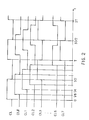
- FIG. 2 illustrates the waveforms of the output signals CL0, CL1, CL2, CL3, ..., CL6 and CL7 of the respective delay elements 130, 131, 132, 133, ..., 136 and 137 of the circuit with phase delay 13.
- the signals CL0-CL7 are presented at the output terminal 10b of the circuit 10.
- the feedback terminal 11b of the phase comparator 11 receives a feedback signal FB constituted by the output signal CL7 of the delay circuit 13.
- the comparator 11 therefore compares the phase of the output signal CL7 with that of the input signal CL.
- the two output terminals 11c and 11d of the phase comparator 11 respectively deliver an INC increment signal and a DEC decrement signal.
- the up-down counter 12 supplies the control signal CTL applied to the delay elements 130-137.
- Each delay element is composed, so conventional, of a predetermined number of elementary delay cells.
- the control signal CTL represents a digital value, which is applied to each delay element to vary the duration of the delay.
- the range of possible variation of the duration of the delay of a delay element during a period T of the input signal CL corresponds to a predetermined fraction 1 / P of the maximum extent of the variation of duration of a delay element. In other words, it takes a given whole number P of periods T to pass from one to the other of the extreme values of the maximum extent of variation of the delay of an element.
- the input signal CL is successively delayed by the eight delay elements 130-137.
- the eight successive delays produced by the elements 130-137 are equal and in principle divide the period T of the input signal CL. If this is exactly the case in practice, the signals CL and FB (CL7) entering the phase comparator 11 and applied to the master-slave flip-flops 14 and 15 have the same phase and the same frequency.
- the signals DEC and INC delivered by flip-flops 14 and 15 therefore have the same logic value.
- the up-down counter 12 is therefore not activated and leaves the control signal CTL unchanged. All the output signals CL0-CL7 are correctly phase shifted with respect to each other and with respect to the input signal CL with the same value T / 8.
- a phase shift in the margin m leaves the INC and DEC signals unchanged and is therefore not assimilated to a phase shift to be corrected.
- the margin m can be determined by the establishment times of flip-flops 14 and 15 and / or by relative delays between the data input and clock input signals of each flip-flop, for example.
- the decrement signal DEC has the logic value 0 and the increment signal has the value 1.
- the up-down counter 12 is therefore incremented so that the control signal CTL consequently increases and equally the durations of the delays produced by the elements 130-137.
- the increment signal INC has the value 0 and the decrement signal DEC has the value 1.
- the up-down counter 12 is decremented so that the CTL control signal equitably decreases the durations of the delays produced by the elements 130-137. Consequently, a phase shift beyond the tolerance margin m is corrected at the level of all the delay elements 130-137 to restore the desired phase shifts.
- the digital phase control implemented in the phase-locked circuit 10 according to the invention offers an important advantage. If the input signal CL is interrupted, in principle the feedback signal FB is also interrupted. The flip-flops 14 and 15 of the phase comparator 11 therefore no longer receive a signal on their clock input and therefore each keep the last state of the transmission. Likewise, the up-down counter 12 retains its last state and, consequently, the state of the delay elements 131-138. In other words, the circuit 10 according to the invention retains the last state of the transmission. It follows that the reappearance of the first edge of the input signal CL will immediately produce the correct output signals CL0-CL7 if the frequency of the input signal CL has not changed.
- the delays are adjusted by the up-down counter 12 from the second cycle of the input signal CL, in order to produce the desired output signals CL0-CL7.
- the duration establishing the correct operation of a phase locked circuit according to the invention may be zero, or at worst equal to the aforementioned number P of periods T of the input signal to pass between the two extreme values of the range of variation of the duration of each delay element. Consequently, the starting up of the circuit according to the invention or the awakening of a transmission line is done very briefly.
- a second major advantage lies in the wide operating frequency band of the phase locked circuit according to the invention.
- the width of the band depends essentially on the range of variable delays of each delay element 130-137, as will emerge later with reference to the frequency multiplier according to the invention.
- the input signal CL and the feedback signal FB which are compared by the phase comparator 11 have in principle the same frequency.
- the structure of the comparator 11 can be very simple, like that illustrated.
- the comparator can accommodate a wide operating frequency band.
- the invention solves all the above problems posed by the use of a conventional PLL.
- Another advantage offered by a circuit 10 according to the invention lies in its adaptation to the various forms of the input signal.
- the duty cycle of the input signal can be arbitrary.
- the delay circuit 13 can have any number N of delay elements.
- the delay circuit 13 can be made of a single variable delay element.
- the circuit 10 could for example serve as a device for phase shifting a period T of an input signal CL which can vary over a very wide range. frequency band.
- the delay elements 130-137 may have a different structure than that described above. We know for example delay elements corresponding to the time of crossing a logic gate. The crossing time is controlled by the intensity of the current flowing through the door, or by the value of the load applied to the door. In this case, the up-down counter 12 should be replaced by a control device suitable for the operation of such delay elements.
- the general principle of the invention is therefore that the delay circuit 13 is controlled by the output signal from the phase comparator 11.
- the advantage of the up-down counter 12 and of the delay elements 130-137 described lies notably in their simplicity of structure and operation, their reliability and their adaptation to the phase comparator described. We have seen the advantages of this comparator. Of course, other structures are possible and can be better adapted to those of the control device 12 of the delay circuit 13.
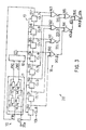
- FIG. 3 illustrates a frequency multiplier 20 according to the invention, implementing the locked circuit in phase 10 shown in FIG. 1.
- the multiplier 20 simply comprises the circuit 10, whose input terminal 10a constitutes the terminal d input 20a of the multiplier 20 and whose output 10b is connected to the input of a logic adder 16.
- the output of the adder 16 constitutes the output terminal 20b of the frequency multiplier 20.
- Figures 3 and 4 illustrate a variant of use in accordance with the invention of the circuit locked in phase 10. According to this variant, the phase comparator 11 incorporates two master-slave flip-flops 14 ′, 15 ′ triggering on the falling edges of the input signal CL.
- the flip-flops 14 ′ and 15 ′ are arranged in the same way as the flip-flops 14 and 15 triggering on the rising edges of the input signal CL. Thanks to this variant, the phase comparison is made every half-periods T / 2 of the input signal CL. Therefore, the output signals CL0-CL7 are successively offset with respect to each edge of the square input signal CL with a duration T / 16 produced by each delay element 130-137.
- the adder 16 is conventionally made of a shaft assembly of seven doors OR Exclusive 160-166 with two inputs.
- the four doors 160-163 respectively receive the output signals CL0 and CL4, CL1 and CL5, CL2 and CL6, CL3 and CL7.
- the gates 160-163 respectively deliver the output signals 2CL0-2CL3 shown in FIG. 4.
- the signals 2CL0-2CL3 are square, having a frequency twice that of the input signal CL.
- the gates 164 and 165 respectively receive the output signals from the gates 160, 162 and 161, 163 and deliver the signals 4CL0 and 4CL1 represented in FIG. 4.
- the signals 4CL0 and 4CL1 are square, having a frequency four times that of the signal d 'entry CL.
- Their application to the last gate 166 provides the output signal 8CL0 on the output terminal 20b of the multiplier 20. As shown in FIG. 4, the signal 8CL0 is square and has a frequency eight times higher than that of the input signal CL .
- the realization in integrated circuits of the logic adder 16 must confer equal propagation times between the outputs of the delay elements 130-137 and the output 20b of the adder. This constraint ensures the quality of the multiple frequency.
- the use of the adder 16 as illustrated requires phase shifts of T / 16 between the signals CL and CL0-CL7. In the multiplier 20 receiving a square input signal, these shifts are simply produced by eight delay elements adjusted at each half-period T / 2 after phase comparison in the comparator 11.
- the frequency multiplier 20 takes advantage of all the advantages of the circuit locked in phase 10 and of those of a logic adder. These include simplicity, reliability and adaptation to a wide operating frequency band. For example, with an input signal CL of period T varying between 5 ns and 10 ns and with a delay circuit 13 of ten delay elements which can each produce a delay varying from 250 to 500 ps, it is possible to obtain at the output of a frequency multiplier according to the invention a frequency included in a band from 1 to 2 GHz.
- the multiplication factor depends on the number N of delay elements in the delay circuit 13, of the operation of the circuit locked in phase 10 and of the structure of the logic adder 16. For example, we could remove the two flip-flops 14 ′ and 15 ′ in the phase comparator 11 and proceed phase comparison at each period T after two passages in elements 130-137. If the input signal CL is not square, we could for example have sixteen delay elements in circuit 10 of FIG. 1, or add an interface between circuit 10 and logic adder 16 in the frequency multiplier 20.
- FIG. 5 schematically illustrates an alternative embodiment of the frequency multiplier 20. All the components have the same structure as that described previously with reference to FIG. 3.
- the circuit locked in phase 10 provides the adder logic 16 all the output signals of the eight delay elements 130-137.
- the only difference between the variant embodiment and that shown in FIG. 3 is the addition of a device for selection such as a multiplexer 17 and in the adaptation to the multiplexer of the links between the delay elements 130-137.
- the multiplexer 17 supplies the feedback signal FB to the feedback input of the phase comparator 11.
- the inputs of the multiplexer 17 are represented diagrammatically by switches connecting the delay elements to each other and associated with the line providing the FB feedback signal.
- the advantage of the multiplexer 17 is to vary the multiplication factor of the frequency multiplier 20.
- the delay elements 136 and 137 are separated by the multiplexer 17, but their respective outputs remain connected to the adder 16 and provide it with a predetermined fixed logic value.
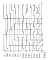
- FIG. 6 illustrates the waveforms of the signals sampled under these conditions from the frequency multiplier 20.
- the signals CL0-CL7 are successively delayed by the duration T / 16 relative to the input signal CL.
- Doors 160-163 provide intermediate signals XCL0-XCL3 to doors 164 and 165.
Abstract
Description
L'invention se rapporte à un circuit verrouillé en phase et à un multiplieur de fréquence en résultant.The invention relates to a circuit locked in phase and to a resulting frequency multiplier.
Le circuit classique verrouillé en phase est désigné couramment par l'acronyme PLL (Phase Locked Loop). Un PLL comprend : un comparateur de phase recevant le signal d'entrée et un signal de contre-réaction ; un filtre recevant le signal de sortie du comparateur de phase ; et un oscillateur commandé en tension, couramment appelé VCO (Voltage Controlled Oscillator), qui reçoit le signal de sortie du filtre, délivre le signal de sortie du PLL et commande une boucle de contre-réaction pour produire le signal de contre-réaction appliqué au comparateur de phase. Le filtre présente une fréquence de coupure relativement basse par rapport à la fréquence de l'oscillateur. L'oscillateur est généralement un générateur d'oscillations libres à une fréquence commandée analogiquement pour varier dans une bande de fréquences prédéterminée. On forme avec ce PLL un multiplieur de fréquence par N, en insérant un diviseur de fréquence par N dans la boucle de contre-réaction.The classic phase locked circuit is commonly known by the acronym PLL (Phase Locked Loop). A PLL comprises: a phase comparator receiving the input signal and a feedback signal; a filter receiving the output signal from the phase comparator; and a voltage controlled oscillator, commonly called a VCO (Voltage Controlled Oscillator), which receives the filter output signal, outputs the PLL output signal and controls a feedback loop to produce the feedback signal applied to the phase comparator. The filter has a relatively low cutoff frequency compared to the frequency of the oscillator. The oscillator is generally a generator of free oscillations at a frequency controlled analogically to vary in a predetermined frequency band. This PLL forms a frequency multiplier by N, by inserting a frequency divider by N in the feedback loop.
L'emploi d'un PLL présente plusieurs inconvénients majeurs. Le premier inconvénient réside dans la durée relativement longue pour obtenir un verrouillage de phase stable sur la fréquence de fonctionnement désirée du PLL. Cet inconvénient se présente au moment de la mise en marche du PLL, ou lors d'un changement de la fréquence de fonctionnement désirée du PLL. La durée d'établissement à un fonctionnement stable du PLL est due à la présence de la boucle de contre-réaction et dépend des caractéristiques électriques du PLL. La caractéristique la plus importante est la valeur de la fréquence de coupure du filtre par rapport à la fréquence de fonctionnement désirée du PLL. La durée d'établissement est d'autant plus longue que la fréquence de coupure est basse. Cependant, l'efficacité du verrouillage de phase est d'autant meilleure que la fréquence de coupure du filtre est basse. Par conséquent, il faut concéder un délai relativement important pour l'établissement du fonctionnement correct d'un PLL. Ce délai est ordinairement de plusieurs millisecondes et correspond donc au passage de nombreuses données que le PLL ne peut pas traiter.The use of a PLL has several major drawbacks. The first drawback lies in the relatively long time required to obtain stable phase locking on the desired operating frequency of the PLL. This drawback occurs when the PLL is switched on, or when the desired PLL operating frequency is changed. The duration of establishment at stable operation of the PLL is due to the presence of the feedback loop and depends on the electrical characteristics of the PLL. The most important characteristic is the value of the cut-off frequency of the filter compared to the desired operating frequency of the PLL. The duration of establishment is all the more long as the cutoff frequency is low. However, the efficiency of phase locking is all the better when the cut-off frequency of the filter is low. Consequently, a relatively long time must be allowed for establishing the correct functioning of a PLL. This delay is usually several milliseconds and therefore corresponds to the passage of numerous data that the PLL cannot process.
Un second inconvénient de l'emploi d'un PLL est sa sensibilité aux bruits éléctriques induits sur le signal analogique de commande du VCO, qui produisent une instabilité temporaire (jitter) de la fréquence de sortie du PLL.A second disadvantage of using a PLL is its sensitivity to electrical noise induced on the analog VCO control signal, which produces a temporary jitter of the PLL output frequency.
Comme troisiéme inconvénient, la bande de fréquences de fonctionnement d'un PLL est relativement étroite pour deux raisons. D'une part, les deux signaux d'entrée du comparateur de phase n'ont pas la même phase et la même fréquence. La réalisation d'un comparateur à large bande de fréquence et de phase s'avère très difficile et très encombrante dans un circuit intégré. D'autre part, on a vu que la commande analogique de l'oscillateur est très sensible aux bruits électriques. Par conséquent, les bruits intervenant dans une large bande de fréquences induiraient de trop grandes variations de fréquences dans le signal de sortie et compromettraient la stabilité de fonctionnement du PLL.As a third drawback, the operating frequency band of a PLL is relatively narrow for two reasons. On the one hand, the two input signals of the phase comparator do not have the same phase and the same frequency. The realization of a broadband frequency and phase comparator proves to be very difficult and very bulky in an integrated circuit. On the other hand, we have seen that the analog control of the oscillator is very sensitive to electrical noise. Consequently, noises occurring in a wide frequency band would induce too large frequency variations in the output signal and would compromise the operating stability of the PLL.
La commande de phase analogique de l'oscillateur d'un PLL est aussi la cause d'un quatrième inconvénient. Cet inconvénient est particulièrement mis en relief dans l'exemple suivant. Actuellement, l'activation d'une liaison de transmission dans un circuit intégré produit une dissipation thermique relativement élevée, de l'ordre de 0,5 watt par exemple. Par conséquent, si on veut y intégrer un nombre important (32 par exemple) de liaisons, il est seulement possible d'en activer un petit nombre (4 ou 8). Un procédé consiste à mettre en sommeil les autres liaisons et à les réveiller sélectivement pour les activer. Etant donné que le réveil doit se faire en un temps très court, il faut mettre numériquement en mémoire tous les réglages propres à chaque liaison. La commande de phase analogique d'un PLL interdit donc un réveil rapide des liaisons. Cet inconvénient se cumule avec le premier inconvénient cité.The analog phase control of a PLL oscillator is also the cause of a fourth drawback. This drawback is particularly highlighted in the following example. Currently, the activation of a transmission link in an integrated circuit produces a relatively high heat dissipation, of the order of 0.5 watt for example. Therefore, if you want to integrate a large number (32 for example) of links, it is only possible to activate a small number (4 or 8). One method is to put the other links to sleep and selectively wake them up to activate them. Since the alarm clock must be done in a very short time, it is necessary to digitally store in memory all the settings specific to each link. The analog phase control of a PLL therefore prohibits rapid reawakening of the links. This drawback is combined with the first drawback mentioned.
L'invention remédie à tous ces inconvénients, en présentant un circuit verrouillé en phase et un multiplieur de fréquence ayant une brève durée d'établissement du fonctionnement correct, insensibles aux bruits électriques, applicables à une large bande de fréquences de fonctionnement et pourvus d'une commande numérique.The invention remedies all these drawbacks by presenting a circuit locked in phase and a frequency multiplier having a short duration of establishment of correct operation, insensitive to electrical noise, applicable to a wide band of operating frequencies and provided with a digital control.
L'invention présente un circuit verrouillé en phase, comprenant un comparateur de phase recevant un signal d'entrée et un signal de contre-réaction, caractérisé en ce que le signal de contre-réaction est produit par un circuit à retard de phase variable du signal d'entrée, dont le retard est commandé par le signal de sortie du comparateur de phase.The invention presents a phase locked circuit comprising a phase comparator receiving an input signal and a feedback signal, characterized in that the feedback signal is produced by a variable phase delay circuit of the input signal, the delay of which is controlled by the output signal of the phase comparator.
Il en résulte un multiplieur de fréquence conforme à l'invention, comprenant un comparateur de phase recevant un signal d'entrée et un signal de contre-réaction, caractérisé en ce que le signal de contre-réaction est produit par un circuit à retard produisant des retards successifs de phase du signal d'entrée commandés par le signal de sortie du comparateur de phase, et en ce que le signal de sortie du multiplieur est délivré par un additionneur logique des signaux retardés.The result is a frequency multiplier according to the invention, comprising a phase comparator receiving an input signal and a feedback signal, characterized in that the feedback signal is produced by a delay circuit producing successive phase delays of the input signal controlled by the output signal of the phase comparator, and in that the output signal of the multiplier is delivered by a logic adder of the delayed signals.
Les caractéristiques et avantages de l'invention ressortent clairement de la description qui suit, donnée à titre d'exemple et faite en référence aux dessins annexés.The characteristics and advantages of the invention appear clearly from the description which follows, given by way of example and made with reference to the accompanying drawings.
Dans les dessins :
- la figure 1 illustre schématiquement un circuit verrouillé en phase conforme à l'invention ;
- la figure 2 présente diverses formes d'onde de signaux prélevés du circuit verrouillé en phase représenté sur la figure 1 afin d'en illustrer le fonctionnement ;
- la figure 3 illustre schématiquement un multiplieur de fréquence conforme à l'invention, résultant de la mise en oeuvre du circuit verrouillé en phase représenté sur la figure 1 ;
- la figure 4 présente diverses formes d'onde de signaux prélevés du multiplieur de fréquence représenté sur la figure 3 afin d'en illustrer le fonctionnement ;
- la figure 5 illustre schématiquement une variante de réalisation d'un multiplieur de fréquence conforme à l'invention ; et
- la figure 6 présente des formes d'ondes de signaux prélevés du multiplieur de fréquence représenté sur la figure 5 pour en illustrer le fonctionnement.
- Figure 1 schematically illustrates a phase locked circuit according to the invention;
- FIG. 2 shows various waveforms of signals taken from the phase locked circuit shown in FIG. 1 in order to illustrate their operation;
- Figure 3 schematically illustrates a frequency multiplier according to the invention, resulting from the implementation of the phase locked circuit shown in Figure 1;
- FIG. 4 shows various waveforms of signals taken from the frequency multiplier shown in FIG. 3 in order to illustrate their operation;
- Figure 5 schematically illustrates an alternative embodiment of a frequency multiplier according to the invention; and
- FIG. 6 shows waveforms of signals taken from the frequency multiplier shown in FIG. 5 to illustrate its operation.
La figure 1 illustre un mode de réalisation préféré d'un circuit verrouillé en phase 10 conforme à l'invention. Le circuit 10 comprend : une borne d'entrée 10a ; un comparateur de phase 11 ayant une première borne d'entrée 11a connectée à la borne d'entrée 10a du circuit 10, une seconde borne d'entrée 11b et deux bornes de sortie 11c, 11d ; un compteur-décompteur 12 ayant deux bornes d'entrée 12a, 12b connectées respectivement aux bornes de sortie 11c, 11d du comparateur de phase 11 et une borne de sortie 12c ; un circuit à retard de phase 13 composé de huit éléments de retard 130-137 connectés en série entre les deux bornes d'entrée 11a et 11b du comparateur de phase 11 et pourvus chacun d'une borne de commande connectée à la borne de sortie 12c du compteur-décompteur 12 ; et une sortie 10b formée par les bornes de sortie respectives des éléments de retard 130-137.FIG. 1 illustrates a preferred embodiment of a circuit locked in
Le comparateur de phase 11 se compose de deux bascules maître-esclave 14 et 15 sensibles aux fronts montants. La bascule 14 a son entrée de données connectée à la borne d'entrée 11a, son entrée d'horloge connectée à la borne d'entrée 11b, et sa sortie connectée à la borne de sortie 11d. La bascule 15 a, de façon similaire, son entrée de données connectée à la borne d'entrée 11b, son entrée d'horloge connectée à la borne d'entrée 11a et sa sortie connectée à la borne de sortie 11c.The
La borne d'entrée 10a du circuit 10 reçoit un signal d'entrée CL de fréquence donnée correspondant à une période T et constituant ordinairement un signal d'horloge. La figure 2 représente un exemple de forme d'onde du signal d'entrée CL par rapport à l'axe des temps t. Dans la figure 2, il est supposé que le signal d'entrée CL est appliqué à l'instant t = 0 sur la borne d'entrée 10a. La figure 2 illustre les formes d'onde des signaux de sortie CL0, CL1, CL2, CL3,..., CL6 et CL7 des éléments de retard respectifs 130, 131, 132, 133,..., 136 et 137 du circuit à retard de phase 13. Les signaux CL0-CL7 sont présentés à la borne de sortie 10b du circuit 10. La borne de contre-réaction 11b du comparateur de phase 11 reçoit un signal de contre-réaction FB constitué par le signal de sortie CL7 du circuit à retard 13. Le comparateur 11 compare donc la phase du signal de sortie CL7 avec celle du signal d'entrée CL. Les deux bornes de sortie 11c et 11d du comparateur de phase 11 délivrent respectivement un signal d'incrémentation INC et un signal de décrémentation DEC. En réponse, le compteur-décompteur 12 fournit le signal de commande CTL appliqué aux éléments de retard 130-137. Chaque élément de retard se compose, de manière classique, d'un nombre prédéterminé de cellules de retard élémentaire. Le signal de commande CTL représente une valeur numérique, qui est appliquée à chaque élément de retard pour en faire varier la durée du retard. La plage de variation possible de la durée du retard d'un élément de retard au cours d'une période T du signal d'entrée CL correspond à une fraction prédéterminée 1/P de l'étendue maximale de la variation de durée d'un élément de retard. En d'autres termes, il faut un nombre entier donné P de périodes T pour passer de l'une à l'autre des valeurs extrêmes de l'étendue maximale de variation du retard d'un élément.The
En fonctionnement, le signal d'entrée CL est retardé successivement par les huit éléments de retard 130-137. Les huit retards successifs produits par les éléments 130-137 sont égaux et divisent en principe la période T du signal d'entrée CL. S'il en est exactement ainsi en pratique, les signaux CL et FB (CL7) entrant dans le comparateur de phase 11 et appliqués aux bascules maître-esclave 14 et 15 ont la même phase et la même fréquence. Les signaux DEC et INC délivrés par les bascules 14 et 15 ont donc la même valeur logique. Le compteur-décompteur 12 n'est donc pas activé et laisse le signal de commande CTL inchangé. Tous les signaux de sortie CL0-CL7 sont correctement déphasés les uns par rapport aux autres et par rapport au signal d'entrée CL d'une même valeur T/8. En pratique, on détermine une marge de tolérance m de déphasage entre le signal d'entrée CL et le signal de contre-réaction FB = CL7. Un déphasage dans la marge m laisse les signaux INC et DEC inchangés et n'est donc pas assimilé à un déphasage à corriger. La marge m peut être déterminée par les temps d'établissement des bascules 14 et 15 et/ou par des retards relatifs entre les signaux d'entrée de données et d'entrée d'horloge de chaque bascule, par exemple. La largeur de la marge m détermine la précision de la comparaison de phase effectuée par le comparateur 11. Elle est typiquement de l'ordre de 50ps pour une période T = 5 ns du signal d'entrée CL.In operation, the input signal CL is successively delayed by the eight delay elements 130-137. The eight successive delays produced by the elements 130-137 are equal and in principle divide the period T of the input signal CL. If this is exactly the case in practice, the signals CL and FB (CL7) entering the
Si le signal de contre-réaction FB est en avance de phase sur le signal d'entrée CL, le signal de décrémentation DEC a la valeur logique 0 et le signal d'incrémentation a la valeur 1. Le compteur-décompteur 12 est donc incrémenté pour que le signal de commande CTL augmente en conséquence et de manière égale les durées des retards produits par les éléments 130-137. Au contraire, si le signal de contre-réaction FB est en retard sur le signal d'entrée CL, le signal d'incrémentation INC a la valeur 0 et le signal de décrémentation DEC a la valeur 1. Le compteur-décompteur 12 est décrémenté pour que le signal de commande CTL diminue équitablement les durées des retards produits par les éléments 130-137. Par conséquent, un déphasage au-delà de la marge de tolérance m est corrigé au niveau de tous les éléments de retard 130-137 pour rétablir les déphasages désirés.If the feedback signal FB is phase ahead of the input signal CL, the decrement signal DEC has the
La commande de phase numérique mise en oeuvre dans le circuit verrouillé en phase 10 conforme à l'invention offre un avantage important. Si le signal d'entrée CL est interrompu, par principe le signal de contre-réaction FB est aussi interrompu. Les bascules 14 et 15 du comparateur de phase 11 ne reçoivent donc plus de signal sur leur entrée d'horloge et conservent donc chacune le dernier état de la transmission. De même, le compteur-décompteur 12 conserve son dernier état et, par conséquent, l'état des éléments de retard 131-138. En d'autres termes, le circuit 10 conforme à l'invention conserve le dernier état de la transmission. Il s'ensuit que la réapparition du premier front du signal d'entrée CL produira immédiatement les signaux de sortie CL0-CL7 corrects si la fréquence du signal d'entrée CL n'a pas changé. Sinon, les retards sont réglés par le compteur-décompteur 12 dès le second cycle du signal d'entrée CL, en vue de produire les signaux de sortie CL0-CL7 désirés. En conclusion, la durée d'établissement du fonctionnement correct d'un circuit verrouillé en phase conforme à l'invention peut être nulle, ou au pire égale au nombre P précité de périodes T du signal d'entrée pour passer entre les deux valeurs extrêmes de l'étendue de variation de la durée de chaque élément de retard. Par conséquent, la mise en marche du circuit conforme à l'invention ou le réveil d'une ligne de transmission se font très brièvement.The digital phase control implemented in the phase-locked
Un second avantage majeur réside dans la large bande de fréquences de fonctionnement du circuit verrouillé en phase conforme à l'invention. La largeur de la bande dépend essentiellement de la gamme de retards variables de chaque élément de retard 130-137, comme cela ressortira ultérieurement en référence au multiplieur de fréquence conforme à l'invention.A second major advantage lies in the wide operating frequency band of the phase locked circuit according to the invention. The width of the band depends essentially on the range of variable delays of each delay element 130-137, as will emerge later with reference to the frequency multiplier according to the invention.
Comme autre grand avantage, le signal d'entrée CL et le signal de contre-réaction FB qui sont comparés par le comparateur de phase 11 ont par principe la même fréquence. La structure du comparateur 11 peut être très simple, comme celle illustrée. En outre, le comparateur peut s'accommoder à une grande bande de fréquences de fonctionnement. En résumé, l'invention résout tous les problèmes précités que posent l'emploi d'un PLL classique. Un autre avantage offert par un circuit 10 conforme à l'invention réside dans son adaptation aux diverses formes du signal d'entrée. Dans l'exemple illustré, le rapport cyclique du signal d'entrée peut être quelconque.As another great advantage, the input signal CL and the feedback signal FB which are compared by the
De nombreuses variantes de réalisation peuvent être apportées au circuit 10 décrit et illustré. Notamment, il est clair que le circuit à retard 13 peut avoir un nombre quelconque N d'éléments de retard. A la limite, le circuit à retard 13 peut être fait d'un seul élément de retard variable. Dans ce cas, le circuit 10 pourrait par exemple servir de dispositif de déphasage d'une période T d'un signal d'entrée CL pouvant varier dans une très large bande de fréquences. En outre, les éléments de retard 130-137 peuvent avoir une autre structure que celle décrite précédemment. On connait par exemple des éléments de retard correspondant au temps de traversée d'une porte logique. Le temps de traversée est commandé par l'intensité du courant qui traverse la porte, ou par la valeur de la charge appliquée à la porte. Dans ce cas, le compteur-décompteur 12 devrait être remplacé par un dispositif de commande approprié au fonctionnement de tels éléments de retard. Le principe général de l'invention est donc que le circuit à retard 13 est commandé par le signal de sortie du comparateur de phase 11. L'avantage du compteur-décompteur 12 et des éléments de retard 130-137 décrits réside notamment dans leur simplicité de structure et de fonctionnement, leur fiabilité et leur adaptation au comparateur de phase décrit. On a vu les avantages de ce comparateur. Bien entendu, d'autres structures sont possibles et peuvent être mieux adaptées à celles du dispositif de commande 12 du circuit à retard 13.Many alternative embodiments can be made to the
La figure 3 illustre un multiplieur de fréquence 20 conforme à l'invention, mettant en oeuvre le circuit verrouillé en phase 10 représenté sur la figure 1. Le multiplieur 20 comprend simplement le circuit 10, dont la borne d'entrée 10a constitue la borne d'entrée 20a du multiplieur 20 et dont la sortie 10b est connectée à l'entrée d'un additionneur logique 16. La sortie de l'additionneur 16 constitue la borne de sortie 20b du multiplieur de fréquence 20. Les figures 3 et 4 illustrent une variante d'utilisation conforme à l'invention du circuit verrouillé en phase 10. Selon cette variante, le comparateur de phase 11 incorpore deux bascules maître-esclave 14′, 15′ déclenchant sur les fronts descendants du signal d'entrée CL. Les bascules 14′ et 15′ sont disposées de la même manière que les bascules 14 et 15 déclenchant sur les fronts montants du signal d'entrée CL. Grâce à cette variante, la comparaison de phase se fait toutes les demi-périodes T/2 du signal d'entrée CL. Par conséquent, les signaux de sortie CL0-CL7 sont successivement décalés par rapport à chaque front du signal d'entrée carré CL d'une durée T/16 produite par chaque élément de retard 130-137.FIG. 3 illustrates a
L'additionneur 16 est fait de manière classique d'un montage en arbre de sept portes OU Exclusif 160-166 à deux entrées. Les quatre portes 160-163 reçoivent respectivement les signaux de sortie CL0 et CL4, CL1 et CL5, CL2 et CL6, CL3 et CL7. Les portes 160-163 délivrent respectivement les signaux de sortie 2CL0-2CL3 représentés sur la figure 4. Les signaux 2CL0-2CL3 sont carrés, ayant une fréquence double de celle du signal d'entrée CL. Les portes 164 et 165 reçoivent respectivement les signaux de sortie des portes 160, 162 et 161, 163 et délivrent les signaux 4CL0 et 4CL1 représentés sur la figure 4. Les signaux 4CL0 et 4CL1 sont carrés, ayant une fréquence quadruple de celle du signal d'entrée CL. Leur application sur la dernière porte 166 fournit le signal de sortie 8CL0 sur la borne de sortie 20b du multiplieur 20. Comme représenté sur la figure 4, le signal 8CL0 est carré et a une fréquence huit fois supérieure à celle du signal d'entrée CL.The
En pratique, la réalisation en circuits intégrés de l'additionneur logique 16 doit conférer des temps de propagation égaux entre les sorties des éléments de retard 130-137 et la sortie 20b de l'additionneur. Cette contrainte assure la qualité de la fréquence multiple. D'autre part, l'emploi de l'additionneur 16 tel qu'illustré nécessite des décalages de phase de T/16 entre les signaux CL et CL0-CL7. Dans le multiplieur 20 recevant un signal d'entrée carré, ces décalages sont simplement produits par huit éléments de retard réglés à chaque demi-période T/2 après comparaison de phase dans le comparateur 11.In practice, the realization in integrated circuits of the
Le multiplieur de fréquence 20 profite de tous les avantages du circuit verrouillé en phase 10 et de ceux d'un additionneur logique. On citera notamment la simplicité, la fiabilité et l'adaptation à une large bande de fréquences de fonctionnement. Par exemple, avec un signal d'entrée CL de période T variant entre 5 ns et 10 ns et avec un circuit à retard 13 de dix éléments de retard pouvant produire chacun un retard variant de 250 à 500 ps, il est possible d'obtenir à la sortie d'un multiplieur de fréquence conforme à l'invention une fréquence comprise dans une bande de 1 à 2GHz.The
En plus des variantes de réalisation citées en référence au circuit verrouillé en phase 10 s'ajoutent toutes les variantes de réalisation bien connues de l'additionneur logique 16. Il est clair aussi que le facteur de multiplication dépend du nombre N d'éléments de retard dans le circuit à retard 13, du fonctionnement du circuit verrouillé en phase 10 et de la structure de l'additionneur logique 16. Par exemple, on pourrait supprimer les deux bascules 14′ et 15′ dans le comparateur de phase 11 et procéder à la comparaison de phase à chaque période T après deux passages dans les éléments 130-137. Si le signal d'entrée CL n'est pas carré, on pourrait par exemple disposer seize éléments de retard dans le circuit 10 de la figure 1, ou ajouter une interface entre le circuit 10 et l'additionneur logique 16 dans le multiplieur de fréquence 20.In addition to the variant embodiments cited with reference to the circuit locked in
La figure 5 illustre schématiquement une variante de réalisation du multiplieur de fréquence 20. Tous les composants ont la même structure que celle décrite précédemment en référence à la figure 3. En d'autres termes, le ciruit verrouillé en phase 10 fournit à l'additionneur logique 16 tous les signaux de sortie des huit éléments de retard 130-137. La seule différence de la variante de réalisation avec celle représentée sur la figure 3 réside dans l'addition d'un dispositif de sélection tel qu'un multiplexeur 17 et dans l'adaptation au multiplexeur des liaisons entre les éléments de retard 130-137. Le multiplexeur 17 fournit le signal de contre-réaction FB à l'entrée de contre-réaction du comparateur de phase 11. Les entrées du multiplexeur 17 sont représentées schématiquement par des commutateurs reliant les éléments de retard entre eux et associés à la ligne fournissant le signal de contre-réaction FB. L'avantage du multiplexeur 17 est de faire varier le facteur de multiplication du multiplieur de fréquence 20. Dans l'exemple choisi et illustré dans les figures 5 et 6, le multiplexeur 17 maintient la liaison des six premiers éléments de retard 130-135 pour prélever le signal de contre-réaction FB à la sortie de l'élément 135 (FB = CL5). Les éléments de retard 136 et 137 sont écartés par le multiplexeur 17, mais leurs sorties respectives restent connectées à l'additionneur 16 et lui fournissent une valeur logique fixe prédéterminée. La figure 6 illustre les formes d'onde des signaux prélevés dans ces conditions du multiplieur de fréquence 20. Les signaux CL0-CL7 sont successivement retardés de la durée T/16 par rapport au signal d'entrée CL. Les portes 160-163 fournissent des signaux intermédiaires XCL0-XCL3 aux portes 164 et 165. Par rapport à la fréquence du signal d'entrée CL, celle des signaux de sortie 3CL0 et 3CL1 des portes 164 et 165 est triple, et celle du signal 6CL0 de la borne 20c est six fois plus grande. Bien sûr, l'homme du métier dispose d'autres variantes de réalisation d'un dispositif de sélection pour obtenir un facteur de multiplication désiré d'un multiplieur de fréquence conforme à l'invention.FIG. 5 schematically illustrates an alternative embodiment of the
Claims (10)
Applications Claiming Priority (2)
| Application Number | Priority Date | Filing Date | Title |
|---|---|---|---|
| FR9001366 | 1990-02-06 | ||
| FR909001366A FR2658015B1 (en) | 1990-02-06 | 1990-02-06 | LOCKED PHASE CIRCUIT AND RESULTING FREQUENCY MULTIPLIER. |
Publications (2)
| Publication Number | Publication Date |
|---|---|
| EP0441684A1 true EP0441684A1 (en) | 1991-08-14 |
| EP0441684B1 EP0441684B1 (en) | 1994-12-28 |
Family
ID=9393432
Family Applications (1)
| Application Number | Title | Priority Date | Filing Date |
|---|---|---|---|
| EP91400225A Expired - Lifetime EP0441684B1 (en) | 1990-02-06 | 1991-01-30 | Phase lock circuit and resulting frequency multiplier |
Country Status (8)
| Country | Link |
|---|---|
| US (3) | US5260608A (en) |
| EP (1) | EP0441684B1 (en) |
| JP (1) | JP3098027B2 (en) |
| CA (1) | CA2051121C (en) |
| DE (1) | DE69106159T2 (en) |
| ES (1) | ES2069229T3 (en) |
| FR (1) | FR2658015B1 (en) |
| WO (1) | WO1991012666A1 (en) |
Cited By (11)
| Publication number | Priority date | Publication date | Assignee | Title |
|---|---|---|---|---|
| EP0655840A2 (en) * | 1993-11-30 | 1995-05-31 | AT&T Corp. | Delay locked loop based clock synthesizer using a dynamically adjustable number of delay elements therein |
| EP0660525A1 (en) * | 1993-12-24 | 1995-06-28 | Bull S.A. | Tree structure with logic gates of the type "Exclusive-OR" and frequency multiplier using the same |
| EP0696116A1 (en) | 1994-08-04 | 1996-02-07 | Bull S.A. | Method for sampling a digital signal |
| EP0771075A2 (en) * | 1995-10-24 | 1997-05-02 | Vlsi Technology, Inc. | Phase locked loop having voltage controlled oscillator utilizing combinational logic |
| EP0800275A1 (en) * | 1996-04-01 | 1997-10-08 | Kabushiki Kaisha Toshiba | A frequency multiplier using a voltage controlled delay circuit |
| EP0800276A1 (en) * | 1996-04-01 | 1997-10-08 | Kabushiki Kaisha Toshiba | A frequency multiplying circuit having a first stage with greater multiplying ratio than subsequent stages |
| WO1998006180A1 (en) * | 1996-08-02 | 1998-02-12 | Rockwell International Corporation | A clock signal frequency multiplier |
| GB2320376A (en) * | 1996-12-11 | 1998-06-17 | Vlsi Technology Inc | Phase locked loop having a voltage controlled oscillator (VCO) with logic stage |
| EP0892497A1 (en) * | 1997-07-16 | 1999-01-20 | STMicroelectronics SA | Method for frequency multiplication of a clock signal with duty cycle control and corresponding device |
| FR2770704A1 (en) * | 1997-11-03 | 1999-05-07 | Sgs Thomson Microelectronics | Phase lock loop method |
| WO2002043246A1 (en) * | 2000-11-21 | 2002-05-30 | Micronas Gmbh | Phase regulating circuit with a time-delay element |
Families Citing this family (76)
| Publication number | Priority date | Publication date | Assignee | Title |
|---|---|---|---|---|
| US6150855A (en) * | 1990-02-06 | 2000-11-21 | Bull, S.A. | Phase-locked loop and resulting frequency multiplier |
| FR2689339B1 (en) * | 1992-03-24 | 1996-12-13 | Bull Sa | MULTI-RANGE DELAY ADJUSTMENT METHOD AND DEVICE. |
| DE69328084T2 (en) * | 1992-12-23 | 2000-08-24 | Conexant Systems Inc | DIGITALLY CONTROLLED PHASE SHIFTER |
| US5422835A (en) * | 1993-07-28 | 1995-06-06 | International Business Machines Corporation | Digital clock signal multiplier circuit |
| FR2710800B1 (en) * | 1993-09-27 | 1995-12-15 | Sgs Thomson Microelectronics | Digital delay line. |
| DE4422802C1 (en) * | 1994-06-29 | 1995-07-20 | Siemens Ag | Frequency multiplier based upon ring oscillator |
| US5815016A (en) * | 1994-09-02 | 1998-09-29 | Xilinx, Inc. | Phase-locked delay loop for clock correction |
| US5646564A (en) * | 1994-09-02 | 1997-07-08 | Xilinx, Inc. | Phase-locked delay loop for clock correction |
| US5640523A (en) * | 1994-09-02 | 1997-06-17 | Cypress Semiconductor Corporation | Method and apparatus for a pulsed tri-state phase detector for reduced jitter clock recovery |
| US5828250A (en) * | 1994-09-06 | 1998-10-27 | Intel Corporation | Differential delay line clock generator with feedback phase control |
| US5537068A (en) * | 1994-09-06 | 1996-07-16 | Intel Corporation | Differential delay line clock generator |
| US5455540A (en) * | 1994-10-26 | 1995-10-03 | Cypress Semiconductor Corp. | Modified bang-bang phase detector with ternary output |
| US5506520A (en) * | 1995-01-11 | 1996-04-09 | International Business Machines Corporation | Energy conserving clock pulse generating circuits |
| US5832279A (en) * | 1995-06-07 | 1998-11-03 | Lsi Logic Corporation | Advanced programmable interrupt controller (APIC) with high speed serial data bus |
| US5721501A (en) * | 1995-07-26 | 1998-02-24 | Kabushiki Kaisha Toshiba | Frequency multiplier and semiconductor integrated circuit employing the same |
| JP3561792B2 (en) * | 1995-09-06 | 2004-09-02 | 株式会社ルネサステクノロジ | Clock generation circuit |
| US5825824A (en) * | 1995-10-05 | 1998-10-20 | Silicon Image, Inc. | DC-balanced and transition-controlled encoding method and apparatus |
| US5999571A (en) * | 1995-10-05 | 1999-12-07 | Silicon Image, Inc. | Transition-controlled digital encoding and signal transmission system |
| US5974464A (en) * | 1995-10-06 | 1999-10-26 | Silicon Image, Inc. | System for high speed serial video signal transmission using DC-balanced coding |
| US5744991A (en) * | 1995-10-16 | 1998-04-28 | Altera Corporation | System for distributing clocks using a delay lock loop in a programmable logic circuit |
| WO1997040576A1 (en) * | 1996-04-25 | 1997-10-30 | Credence Systems Corporation | Frequency multiplier |
| US5786715A (en) * | 1996-06-21 | 1998-07-28 | Sun Microsystems, Inc. | Programmable digital frequency multiplier |
| JPH1022822A (en) * | 1996-07-05 | 1998-01-23 | Sony Corp | Digital pll circuit |
| GB2355096B (en) * | 1996-08-13 | 2001-05-23 | Fujitsu Ltd | Semiconductor device and semiconductor circuitry |
| TW340262B (en) * | 1996-08-13 | 1998-09-11 | Fujitsu Ltd | Semiconductor device, system consisting of semiconductor devices and digital delay circuit |
| JPH10117142A (en) * | 1996-10-11 | 1998-05-06 | Fujitsu Ltd | Phase-locked loop circuit and semiconductor integrated circuit |
| US5933035A (en) * | 1996-12-31 | 1999-08-03 | Cirrus Logic, Inc. | Digital clock frequency multiplication circuit and method |
| KR100214559B1 (en) * | 1997-02-20 | 1999-08-02 | 구본준 | Frequency multiplier |
| JPH10256883A (en) * | 1997-03-06 | 1998-09-25 | Nec Ic Microcomput Syst Ltd | Digital multiplier circuit |
| JP2954070B2 (en) * | 1997-03-26 | 1999-09-27 | 日本電気アイシーマイコンシステム株式会社 | Digital PLL circuit |
| JP3319340B2 (en) | 1997-05-30 | 2002-08-26 | 日本電気株式会社 | Semiconductor circuit device |
| US6100736A (en) * | 1997-06-05 | 2000-08-08 | Cirrus Logic, Inc | Frequency doubler using digital delay lock loop |
| US5889435A (en) * | 1997-06-30 | 1999-03-30 | Sun Microsystems, Inc. | On-chip PLL phase and jitter self-test circuit |
| JPH11110065A (en) | 1997-10-03 | 1999-04-23 | Mitsubishi Electric Corp | Internal clock signal generating circuit |
| US5982213A (en) | 1997-11-14 | 1999-11-09 | Texas Instruments Incorporated | Digital phase lock loop |
| US6023182A (en) * | 1997-12-31 | 2000-02-08 | Intel Corporation | High gain pulse generator circuit with clock gating |
| US5963071A (en) * | 1998-01-22 | 1999-10-05 | Nanoamp Solutions, Inc. | Frequency doubler with adjustable duty cycle |
| JP3338367B2 (en) * | 1998-03-25 | 2002-10-28 | 沖電気工業株式会社 | Phase comparator |
| JPH11298306A (en) * | 1998-04-16 | 1999-10-29 | Nec Corp | Semiconductor device and delay setting method |
| US6037812A (en) * | 1998-05-18 | 2000-03-14 | National Semiconductor Corporation | Delay locked loop (DLL) based clock synthesis |
| US7564283B1 (en) | 1998-06-22 | 2009-07-21 | Xilinx, Inc. | Automatic tap delay calibration for precise digital phase shift |
| US6040726A (en) * | 1998-09-14 | 2000-03-21 | Lucent Technologies Inc. | Digital duty cycle correction loop apparatus and method |
| US6255878B1 (en) | 1998-09-18 | 2001-07-03 | Lsi Logic Corporation | Dual path asynchronous delay circuit |
| JP3271602B2 (en) * | 1999-02-17 | 2002-04-02 | 日本電気株式会社 | Semiconductor integrated circuit device and its design method |
| CA2270516C (en) | 1999-04-30 | 2009-11-17 | Mosaid Technologies Incorporated | Frequency-doubling delay locked loop |
| US6211708B1 (en) | 1999-06-28 | 2001-04-03 | Ericsson, Inc. | Frequency doubling circuits, method, and systems including quadrature phase generators |
| EP1076435A1 (en) * | 1999-08-12 | 2001-02-14 | STMicroelectronics S.r.l. | A detector for detecting timing in a data flow |
| US6275072B1 (en) * | 1999-10-07 | 2001-08-14 | Velio Communications, Inc. | Combined phase comparator and charge pump circuit |
| DE69929201D1 (en) * | 1999-10-18 | 2006-02-02 | St Microelectronics Srl | Improved delay locked loop |
| US6594330B1 (en) * | 1999-10-26 | 2003-07-15 | Agere Systems Inc. | Phase-locked loop with digitally controlled, frequency-multiplying oscillator |
| US6674772B1 (en) * | 1999-10-28 | 2004-01-06 | Velio Communicaitons, Inc. | Data communications circuit with multi-stage multiplexing |
| US6952431B1 (en) | 1999-10-28 | 2005-10-04 | Rambus Inc. | Clock multiplying delay-locked loop for data communications |
| US6501311B2 (en) * | 2000-01-24 | 2002-12-31 | Broadcom Corporation | System and method for compensating for supply voltage induced signal delay mismatches |
| JP3961195B2 (en) * | 2000-05-30 | 2007-08-22 | 株式会社東芝 | Semiconductor integrated circuit |
| US6768356B1 (en) * | 2000-09-07 | 2004-07-27 | Iowa State University Research Foundation, Inc. | Apparatus for and method of implementing time-interleaved architecture |
| FR2817981B1 (en) * | 2000-12-07 | 2003-02-14 | Bull Sa | MULTIPLIER CIRCUIT OF FRONTS |
| US6535038B2 (en) | 2001-03-09 | 2003-03-18 | Micron Technology, Inc. | Reduced jitter clock generator circuit and method for applying properly phased clock signals to clocked devices |
| WO2003005585A1 (en) * | 2001-07-06 | 2003-01-16 | Telefonaktiebolaget L.M. Ericsson | A signal generator device, method for generating a signal and devices including such a signal generator device |
| CA2375291C (en) * | 2002-03-08 | 2005-05-17 | Sirific Wireless Corporation | Generation of virtual local oscillator inputs for use in direct conversion radio systems |
| US6727764B2 (en) * | 2002-03-08 | 2004-04-27 | Sirific Wireless Corporation | Generation of virtual local oscillator inputs for use in direct conversion radio systems |
| US6653876B2 (en) * | 2002-04-23 | 2003-11-25 | Broadcom Corporation | Method and apparatus for synthesizing a clock signal using a compact and low power delay locked loop (DLL) |
| US6880026B2 (en) * | 2002-05-16 | 2005-04-12 | International Business Machines Corporation | Method and apparatus for implementing chip-to-chip interconnect bus initialization |
| US6996650B2 (en) * | 2002-05-16 | 2006-02-07 | International Business Machines Corporation | Method and apparatus for implementing multiple configurable sub-busses of a point-to-point bus |
| US8340215B2 (en) * | 2002-07-26 | 2012-12-25 | Motorola Mobility Llc | Radio transceiver architectures and methods |
| JP2006503467A (en) * | 2002-10-16 | 2006-01-26 | コーニンクレッカ フィリップス エレクトロニクス エヌ ヴィ | Pulse generator |
| US7372928B1 (en) | 2002-11-15 | 2008-05-13 | Cypress Semiconductor Corporation | Method and system of cycle slip framing in a deserializer |
| US8085857B1 (en) | 2003-09-25 | 2011-12-27 | Cypress Semiconductor Corporation | Digital-compatible multi-state-sense input |
| JP2007521703A (en) * | 2003-12-10 | 2007-08-02 | テレフオンアクチーボラゲット エル エム エリクソン(パブル) | Frequency multiplier |
| US7123063B2 (en) * | 2004-04-28 | 2006-10-17 | Broadcom Corporation | Supply tracking clock multiplier |
| US7202719B2 (en) * | 2004-09-30 | 2007-04-10 | Motorola, Inc. | Method and apparatus for frequency synthesis |
| KR100693895B1 (en) | 2005-08-16 | 2007-03-12 | 삼성전자주식회사 | Clock multiplier having phase-locked loop circuit |
| EP1833173A1 (en) * | 2006-03-06 | 2007-09-12 | Seiko Epson Corporation | Pulse generator and method of genrerating pulses, such as for template generation in impulse radio systems |
| US7719338B2 (en) * | 2007-06-05 | 2010-05-18 | Seiko Epson Corporation | Pulse generating circuit and UWB communication system |
| DE102007057990B3 (en) * | 2007-12-03 | 2009-04-16 | Knorr-Bremse Systeme für Nutzfahrzeuge GmbH | Method and circuit arrangement for monitoring devices triggered by electrical impulses |
| US9966937B2 (en) * | 2011-04-29 | 2018-05-08 | Marvell World Trade Ltd. | Frequency multipliers |
| KR101811280B1 (en) * | 2017-03-28 | 2017-12-22 | 김태오 | A display cabinet equipped with led lights |
Citations (2)
| Publication number | Priority date | Publication date | Assignee | Title |
|---|---|---|---|---|
| EP0102598A1 (en) * | 1979-11-09 | 1984-03-14 | Siemens Nixdorf Informationssysteme Aktiengesellschaft | Device for phase synchronization |
| EP0274606A2 (en) * | 1986-11-21 | 1988-07-20 | Siemens Aktiengesellschaft | Arrangement for creating an integrated CMOS ciruit technique delay network and a phase comparator section |
Family Cites Families (36)
| Publication number | Priority date | Publication date | Assignee | Title |
|---|---|---|---|---|
| FI41662C (en) * | 1964-06-09 | 1970-01-12 | Ericsson Telefon Ab L M | Device in a receiver of pulse code modulated time multiplication signals |
| US3587043A (en) * | 1969-04-29 | 1971-06-22 | Rca Corp | Character parity synchronizer |
| FR2313827A1 (en) * | 1975-06-02 | 1976-12-31 | Materiel Telephonique | Binary elements train transmission system - has simple means of synchronising receiver timer, this timer having multiphase circuit |
| US3992612A (en) * | 1975-10-14 | 1976-11-16 | The United States Of America As Represented By The Secretary Of The Army | Rate multiplier |
| US3993957A (en) * | 1976-03-08 | 1976-11-23 | International Business Machines Corporation | Clock converter circuit |
| US4449119A (en) * | 1981-12-14 | 1984-05-15 | International Business Machines Corporation | Self-clocking serial decoder |
| FR2527029A1 (en) * | 1982-05-14 | 1983-11-18 | Thomson Csf Mat Tel | TRANSMITTER AND DATA RECEIVER IN PACKET MODE |
| JPS59225640A (en) * | 1983-06-06 | 1984-12-18 | Nitsuko Ltd | Clock phase synchronization system |
| FR2567696B1 (en) * | 1984-07-13 | 1991-06-28 | Thomas Alain | DEVICE FOR AUTOMATICALLY FRAMING LOCAL CLOCK IN RELATION TO A DATA SIGNAL AND SAMPLING CIRCUIT COMPRISING AN APPLICATION |
| US4637018A (en) * | 1984-08-29 | 1987-01-13 | Burroughs Corporation | Automatic signal delay adjustment method |
| JPS62175011A (en) * | 1985-10-16 | 1987-07-31 | Fujitsu Ltd | N-multiplying circuit |
| CA1241384A (en) * | 1985-10-18 | 1988-08-30 | Stephen C. Carlton | Serial-to-parallel converter for high-speed bit streams |
| JPH0744448B2 (en) * | 1986-03-31 | 1995-05-15 | 株式会社東芝 | Digital phase synchronization loop circuit |
| US4795985A (en) * | 1986-04-01 | 1989-01-03 | Hewlett-Packard Company | Digital phase lock loop |
| FR2604043B1 (en) * | 1986-09-17 | 1993-04-09 | Cit Alcatel | DEVICE FOR RECORDING ONE OR MORE BINARY DATA TRAINS OF IDENTICAL OR SUB-MULTIPLE RATES ON A SYNCHRONOUS CLOCK REFERENCE SIGNAL |
| US4922141A (en) * | 1986-10-07 | 1990-05-01 | Western Digital Corporation | Phase-locked loop delay line |
| EP0299024A4 (en) * | 1987-01-05 | 1990-11-28 | Grumman Aerospace Corporation | High speed data-clock synchronization processor |
| JPS63258112A (en) * | 1987-04-15 | 1988-10-25 | Fujitsu Ltd | Multiplier circuit |
| JPS63292185A (en) * | 1987-05-25 | 1988-11-29 | 日本電気株式会社 | Digital input/output circuit |
| US4873491A (en) * | 1987-10-19 | 1989-10-10 | Wilkins Jeffrey K | Phase shift circuit utilizing a variable time delay line |
| US4901076A (en) * | 1987-10-29 | 1990-02-13 | International Business Machines Corporation | Circuit for converting between serial and parallel data streams by high speed addressing |
| JPH01152815A (en) * | 1987-12-09 | 1989-06-15 | Nec Corp | Frequency multiplier circuit |
| US4789996A (en) * | 1988-01-28 | 1988-12-06 | Siemens Transmission Systems, Inc. | Center frequency high resolution digital phase-lock loop circuit |
| JP2531742B2 (en) * | 1988-05-17 | 1996-09-04 | 株式会社東芝 | Voltage controlled oscillator |
| JPH0773219B2 (en) * | 1988-06-16 | 1995-08-02 | 富士通株式会社 | Parallel-serial converter |
| JPH01319321A (en) * | 1988-06-20 | 1989-12-25 | Nec Ic Microcomput Syst Ltd | Digital frequency multiplier circuit |
| US5043596A (en) * | 1988-09-14 | 1991-08-27 | Hitachi, Ltd. | Clock signal supplying device having a phase compensation circuit |
| ATE101769T1 (en) * | 1988-10-13 | 1994-03-15 | Siemens Ag | METHOD AND CIRCUIT ARRANGEMENT FOR RECEIVING A BINARY DIGITAL SIGNAL. |
| US5087829A (en) * | 1988-12-07 | 1992-02-11 | Hitachi, Ltd. | High speed clock distribution system |
| JP2635789B2 (en) * | 1989-01-17 | 1997-07-30 | 株式会社東芝 | Signal delay circuit and clock signal generation circuit using the circuit |
| US5118975A (en) * | 1990-03-05 | 1992-06-02 | Thinking Machines Corporation | Digital clock buffer circuit providing controllable delay |
| US5120989A (en) * | 1991-02-04 | 1992-06-09 | The United States Of America As Represented By The Secretary Of The Army | Simplified clock distribution in electronic systems |
| US5079519A (en) * | 1991-02-14 | 1992-01-07 | Notorola, Inc. | Digital phase lock loop for a gate array |
| JPH0590914A (en) * | 1991-02-22 | 1993-04-09 | Mitsubishi Electric Corp | Voltage controlled oscillator |
| JP2861465B2 (en) * | 1991-05-16 | 1999-02-24 | 日本電気株式会社 | Frequency multiplier |
| US5216301A (en) * | 1991-12-20 | 1993-06-01 | Artisoft, Inc. | Digital self-calibrating delay line and frequency multiplier |
-
1990
- 1990-02-06 FR FR909001366A patent/FR2658015B1/en not_active Expired - Fee Related
-
1991
- 1991-01-30 CA CA002051121A patent/CA2051121C/en not_active Expired - Fee Related
- 1991-01-30 US US07/762,018 patent/US5260608A/en not_active Expired - Lifetime
- 1991-01-30 EP EP91400225A patent/EP0441684B1/en not_active Expired - Lifetime
- 1991-01-30 ES ES91400225T patent/ES2069229T3/en not_active Expired - Lifetime
- 1991-01-30 WO PCT/FR1991/000058 patent/WO1991012666A1/en active Application Filing
- 1991-01-30 DE DE69106159T patent/DE69106159T2/en not_active Expired - Fee Related
- 1991-01-30 JP JP03503776A patent/JP3098027B2/en not_active Expired - Fee Related
-
1994
- 1994-10-03 US US08/312,981 patent/US5548235A/en not_active Expired - Lifetime
-
1997
- 1997-08-29 US US08/921,334 patent/US5838178A/en not_active Expired - Lifetime
Patent Citations (2)
| Publication number | Priority date | Publication date | Assignee | Title |
|---|---|---|---|---|
| EP0102598A1 (en) * | 1979-11-09 | 1984-03-14 | Siemens Nixdorf Informationssysteme Aktiengesellschaft | Device for phase synchronization |
| EP0274606A2 (en) * | 1986-11-21 | 1988-07-20 | Siemens Aktiengesellschaft | Arrangement for creating an integrated CMOS ciruit technique delay network and a phase comparator section |
Non-Patent Citations (1)
| Title |
|---|
| IBM TECHNICAL DISCLOSURE BULLETIN. vol. 26, no. 3A, août 1983, NEW YORK US pages 990 - 991; HERNANDEZ: "FREQUENCY MULTIPLIER USING DELAY CIRCUITS" * |
Cited By (20)
| Publication number | Priority date | Publication date | Assignee | Title |
|---|---|---|---|---|
| EP0655840A3 (en) * | 1993-11-30 | 1996-03-27 | At & T Corp | Delay locked loop based clock synthesizer using a dynamically adjustable number of delay elements therein. |
| EP0655840A2 (en) * | 1993-11-30 | 1995-05-31 | AT&T Corp. | Delay locked loop based clock synthesizer using a dynamically adjustable number of delay elements therein |
| EP0660525A1 (en) * | 1993-12-24 | 1995-06-28 | Bull S.A. | Tree structure with logic gates of the type "Exclusive-OR" and frequency multiplier using the same |
| FR2714550A1 (en) * | 1993-12-24 | 1995-06-30 | Bull Sa | Tree of OR-Exclusive logic gates and frequency multiplier incorporating it. |
| US5614841A (en) * | 1993-12-24 | 1997-03-25 | Bull S.A. | Frequency multiplier using XOR/NXOR gates which have equal propagation delays |
| EP0696116A1 (en) | 1994-08-04 | 1996-02-07 | Bull S.A. | Method for sampling a digital signal |
| EP0771075A2 (en) * | 1995-10-24 | 1997-05-02 | Vlsi Technology, Inc. | Phase locked loop having voltage controlled oscillator utilizing combinational logic |
| EP0771075A3 (en) * | 1995-10-24 | 1997-12-03 | Vlsi Technology, Inc. | Phase locked loop having voltage controlled oscillator utilizing combinational logic |
| US5955902A (en) * | 1996-04-01 | 1999-09-21 | Kabushiki Kaisha Toshiba | Frequency multiplier using a voltage controlled delay circuit |
| EP0800275A1 (en) * | 1996-04-01 | 1997-10-08 | Kabushiki Kaisha Toshiba | A frequency multiplier using a voltage controlled delay circuit |
| EP0800276A1 (en) * | 1996-04-01 | 1997-10-08 | Kabushiki Kaisha Toshiba | A frequency multiplying circuit having a first stage with greater multiplying ratio than subsequent stages |
| US6005420A (en) * | 1996-04-01 | 1999-12-21 | Kabushiki Kaisha Toshiba | Frequency multiplying circuit having a greater multiplying ratio |
| WO1998006180A1 (en) * | 1996-08-02 | 1998-02-12 | Rockwell International Corporation | A clock signal frequency multiplier |
| US5821785A (en) * | 1996-08-02 | 1998-10-13 | Rockwell Int'l Corp. | Clock signal frequency multiplier |
| GB2320376A (en) * | 1996-12-11 | 1998-06-17 | Vlsi Technology Inc | Phase locked loop having a voltage controlled oscillator (VCO) with logic stage |
| GB2320376B (en) * | 1996-12-11 | 2001-07-04 | Vlsi Technology Inc | Phase locked loop having a multiple frequency output voltage controlled oscillator |
| EP0892497A1 (en) * | 1997-07-16 | 1999-01-20 | STMicroelectronics SA | Method for frequency multiplication of a clock signal with duty cycle control and corresponding device |
| FR2766305A1 (en) * | 1997-07-16 | 1999-01-22 | St Microelectronics Sa | METHOD FOR MULTIPLYING THE FREQUENCY OF A CLOCK SIGNAL WITH CYCLIC CHECK, AND CORRESPONDING DEVICE |
| FR2770704A1 (en) * | 1997-11-03 | 1999-05-07 | Sgs Thomson Microelectronics | Phase lock loop method |
| WO2002043246A1 (en) * | 2000-11-21 | 2002-05-30 | Micronas Gmbh | Phase regulating circuit with a time-delay element |
Also Published As
| Publication number | Publication date |
|---|---|
| CA2051121A1 (en) | 1991-08-07 |
| JP3098027B2 (en) | 2000-10-10 |
| US5548235A (en) | 1996-08-20 |
| FR2658015A1 (en) | 1991-08-09 |
| WO1991012666A1 (en) | 1991-08-22 |
| CA2051121C (en) | 1996-08-20 |
| US5838178A (en) | 1998-11-17 |
| JPH04505539A (en) | 1992-09-24 |
| FR2658015B1 (en) | 1994-07-29 |
| DE69106159T2 (en) | 1995-05-04 |
| EP0441684B1 (en) | 1994-12-28 |
| US5260608A (en) | 1993-11-09 |
| ES2069229T3 (en) | 1995-05-01 |
| DE69106159D1 (en) | 1995-02-09 |
Similar Documents
| Publication | Publication Date | Title |
|---|---|---|
| EP0441684B1 (en) | Phase lock circuit and resulting frequency multiplier | |
| EP0645888B1 (en) | Digital delay line | |
| FR2668669A1 (en) | CIRCUIT AND METHOD FOR GENERATING TIME SIGNALS. | |
| EP0466591B1 (en) | Method and system for serial digital data communication | |
| EP0800276B1 (en) | A frequency multiplying circuit having a first stage with greater multiplying ratio than subsequent stages | |
| US6150855A (en) | Phase-locked loop and resulting frequency multiplier | |
| FR2787651A1 (en) | DIGITAL PHASE FREQUENCY DETECTOR | |
| US7034591B2 (en) | False-lock-free delay locked loop circuit and method | |
| EP0564377B1 (en) | Frequency locked loop | |
| JP3487533B2 (en) | Multiplier circuit and semiconductor integrated circuit device | |
| FR2713034A1 (en) | Clock recovery circuit with paired oscillators. | |
| FR2841406A1 (en) | VARIABLE DEPHASER CIRCUIT, PHASE INTERPOLATOR INCORPORATING THE SAME, AND DIGITAL FREQUENCY SYNTHESIZER INCORPORATING SUCH AN INTERPOLATOR | |
| EP0639001B1 (en) | Pulse signal filter circuit and integrated circuit with such a circuit | |
| EP0466593B1 (en) | Data sampling circuit and digital data transmission system therefor | |
| FR2773925A1 (en) | Phase lock loop locking condition detection | |
| EP0302562B1 (en) | Frequency synthesizer having a tuning indicator device | |
| EP1606880B1 (en) | Frequency divider with variable division rate | |
| EP3627707A1 (en) | Frequency synthesis device with high multiplication range | |
| US6249160B1 (en) | Clock reproduction and identification apparatus | |
| JPS5957530A (en) | Phase locked loop | |
| US6208182B1 (en) | Phase-locked loop circuit | |
| EP3764546B1 (en) | Frequency synthesis device with feedback loop | |
| EP0991193A1 (en) | Radio apparatus comprising a frequency synthesiser and phase discriminator for such an apparatus | |
| FR2816075A1 (en) | Generator for production of clock signals, comprises frequency divider suppling low frequency signal, comparison unit and initialization circuit to synchronize low frequency and reference signals | |
| FR2864377A1 (en) | Phase locked loop for phase or frequency modulation application, has phase comparator activating measurement signal during measurement time interval that is generated at duration defined by cycle count of high frequency signal |
Legal Events
| Date | Code | Title | Description |
|---|---|---|---|
| PUAI | Public reference made under article 153(3) epc to a published international application that has entered the european phase |
Free format text: ORIGINAL CODE: 0009012 |
|
| 17P | Request for examination filed |
Effective date: 19910531 |
|
| AK | Designated contracting states |
Kind code of ref document: A1 Designated state(s): DE ES FR GB IT NL SE |
|
| RAP3 | Party data changed (applicant data changed or rights of an application transferred) |
Owner name: BULL S.A. |
|
| 17Q | First examination report despatched |
Effective date: 19940217 |
|
| GRAA | (expected) grant |
Free format text: ORIGINAL CODE: 0009210 |
|
| AK | Designated contracting states |
Kind code of ref document: B1 Designated state(s): DE ES FR GB IT NL SE |
|
| ITF | It: translation for a ep patent filed |
Owner name: FUMERO BREVETTI S.N.C. |
|
| EAL | Se: european patent in force in sweden |
Ref document number: 91400225.8 |
|
| REF | Corresponds to: |
Ref document number: 69106159 Country of ref document: DE Date of ref document: 19950209 |
|
| GBT | Gb: translation of ep patent filed (gb section 77(6)(a)/1977) |
Effective date: 19950116 |
|
| REG | Reference to a national code |
Ref country code: ES Ref legal event code: FG2A Ref document number: 2069229 Country of ref document: ES Kind code of ref document: T3 |
|
| PLBE | No opposition filed within time limit |
Free format text: ORIGINAL CODE: 0009261 |
|
| STAA | Information on the status of an ep patent application or granted ep patent |
Free format text: STATUS: NO OPPOSITION FILED WITHIN TIME LIMIT |
|
| 26N | No opposition filed | ||
| REG | Reference to a national code |
Ref country code: GB Ref legal event code: IF02 |
|
| PGFP | Annual fee paid to national office [announced via postgrant information from national office to epo] |
Ref country code: DE Payment date: 20061227 Year of fee payment: 17 |
|
| PGFP | Annual fee paid to national office [announced via postgrant information from national office to epo] |
Ref country code: SE Payment date: 20061228 Year of fee payment: 17 Ref country code: GB Payment date: 20061228 Year of fee payment: 17 |
|
| PGFP | Annual fee paid to national office [announced via postgrant information from national office to epo] |
Ref country code: ES Payment date: 20070116 Year of fee payment: 17 |
|
| PGFP | Annual fee paid to national office [announced via postgrant information from national office to epo] |
Ref country code: IT Payment date: 20070620 Year of fee payment: 17 |
|
| EUG | Se: european patent has lapsed | ||
| GBPC | Gb: european patent ceased through non-payment of renewal fee |
Effective date: 20080130 |
|
| PG25 | Lapsed in a contracting state [announced via postgrant information from national office to epo] |
Ref country code: DE Free format text: LAPSE BECAUSE OF NON-PAYMENT OF DUE FEES Effective date: 20080801 |
|
| PG25 | Lapsed in a contracting state [announced via postgrant information from national office to epo] |
Ref country code: GB Free format text: LAPSE BECAUSE OF NON-PAYMENT OF DUE FEES Effective date: 20080130 |
|
| PG25 | Lapsed in a contracting state [announced via postgrant information from national office to epo] |
Ref country code: SE Free format text: LAPSE BECAUSE OF NON-PAYMENT OF DUE FEES Effective date: 20080131 |
|
| REG | Reference to a national code |
Ref country code: ES Ref legal event code: FD2A Effective date: 20080131 |
|
| PG25 | Lapsed in a contracting state [announced via postgrant information from national office to epo] |
Ref country code: ES Free format text: LAPSE BECAUSE OF NON-PAYMENT OF DUE FEES Effective date: 20080131 |
|
| PG25 | Lapsed in a contracting state [announced via postgrant information from national office to epo] |
Ref country code: IT Free format text: LAPSE BECAUSE OF NON-PAYMENT OF DUE FEES Effective date: 20080130 |
|
| PGFP | Annual fee paid to national office [announced via postgrant information from national office to epo] |
Ref country code: FR Payment date: 20100223 Year of fee payment: 20 |
|
| PGFP | Annual fee paid to national office [announced via postgrant information from national office to epo] |
Ref country code: NL Payment date: 20091228 Year of fee payment: 20 |
|
| REG | Reference to a national code |
Ref country code: NL Ref legal event code: V4 Effective date: 20110130 |
|
| PG25 | Lapsed in a contracting state [announced via postgrant information from national office to epo] |
Ref country code: NL Free format text: LAPSE BECAUSE OF EXPIRATION OF PROTECTION Effective date: 20110130 |