EP0441591A2 - A method for driving a liquid crystal panel - Google Patents
A method for driving a liquid crystal panel Download PDFInfo
- Publication number
- EP0441591A2 EP0441591A2 EP91300930A EP91300930A EP0441591A2 EP 0441591 A2 EP0441591 A2 EP 0441591A2 EP 91300930 A EP91300930 A EP 91300930A EP 91300930 A EP91300930 A EP 91300930A EP 0441591 A2 EP0441591 A2 EP 0441591A2
- Authority
- EP
- European Patent Office
- Prior art keywords
- display
- voltage
- scanning
- electrodes
- lit
- Prior art date
- Legal status (The legal status is an assumption and is not a legal conclusion. Google has not performed a legal analysis and makes no representation as to the accuracy of the status listed.)
- Granted
Links
Images


Classifications
-
- H—ELECTRICITY
- H04—ELECTRIC COMMUNICATION TECHNIQUE
- H04N—PICTORIAL COMMUNICATION, e.g. TELEVISION
- H04N3/00—Scanning details of television systems; Combination thereof with generation of supply voltages
- H04N3/10—Scanning details of television systems; Combination thereof with generation of supply voltages by means not exclusively optical-mechanical
- H04N3/12—Scanning details of television systems; Combination thereof with generation of supply voltages by means not exclusively optical-mechanical by switched stationary formation of lamps, photocells or light relays
- H04N3/127—Scanning details of television systems; Combination thereof with generation of supply voltages by means not exclusively optical-mechanical by switched stationary formation of lamps, photocells or light relays using liquid crystals
-
- G—PHYSICS
- G09—EDUCATION; CRYPTOGRAPHY; DISPLAY; ADVERTISING; SEALS
- G09G—ARRANGEMENTS OR CIRCUITS FOR CONTROL OF INDICATING DEVICES USING STATIC MEANS TO PRESENT VARIABLE INFORMATION
- G09G3/00—Control arrangements or circuits, of interest only in connection with visual indicators other than cathode-ray tubes
- G09G3/20—Control arrangements or circuits, of interest only in connection with visual indicators other than cathode-ray tubes for presentation of an assembly of a number of characters, e.g. a page, by composing the assembly by combination of individual elements arranged in a matrix no fixed position being assigned to or needed to be assigned to the individual characters or partial characters
- G09G3/34—Control arrangements or circuits, of interest only in connection with visual indicators other than cathode-ray tubes for presentation of an assembly of a number of characters, e.g. a page, by composing the assembly by combination of individual elements arranged in a matrix no fixed position being assigned to or needed to be assigned to the individual characters or partial characters by control of light from an independent source
- G09G3/36—Control arrangements or circuits, of interest only in connection with visual indicators other than cathode-ray tubes for presentation of an assembly of a number of characters, e.g. a page, by composing the assembly by combination of individual elements arranged in a matrix no fixed position being assigned to or needed to be assigned to the individual characters or partial characters by control of light from an independent source using liquid crystals
- G09G3/3611—Control of matrices with row and column drivers
- G09G3/3622—Control of matrices with row and column drivers using a passive matrix
-
- G—PHYSICS
- G09—EDUCATION; CRYPTOGRAPHY; DISPLAY; ADVERTISING; SEALS
- G09G—ARRANGEMENTS OR CIRCUITS FOR CONTROL OF INDICATING DEVICES USING STATIC MEANS TO PRESENT VARIABLE INFORMATION
- G09G2320/00—Control of display operating conditions
- G09G2320/02—Improving the quality of display appearance
- G09G2320/0209—Crosstalk reduction, i.e. to reduce direct or indirect influences of signals directed to a certain pixel of the displayed image on other pixels of said image, inclusive of influences affecting pixels in different frames or fields or sub-images which constitute a same image, e.g. left and right images of a stereoscopic display
-
- G—PHYSICS
- G09—EDUCATION; CRYPTOGRAPHY; DISPLAY; ADVERTISING; SEALS
- G09G—ARRANGEMENTS OR CIRCUITS FOR CONTROL OF INDICATING DEVICES USING STATIC MEANS TO PRESENT VARIABLE INFORMATION
- G09G2320/00—Control of display operating conditions
- G09G2320/02—Improving the quality of display appearance
- G09G2320/0247—Flicker reduction other than flicker reduction circuits used for single beam cathode-ray tubes
-
- G—PHYSICS
- G09—EDUCATION; CRYPTOGRAPHY; DISPLAY; ADVERTISING; SEALS
- G09G—ARRANGEMENTS OR CIRCUITS FOR CONTROL OF INDICATING DEVICES USING STATIC MEANS TO PRESENT VARIABLE INFORMATION
- G09G2320/00—Control of display operating conditions
- G09G2320/04—Maintaining the quality of display appearance
- G09G2320/041—Temperature compensation
Definitions
- the present invention relates to a method for driving a liquid crystal panel.
- a driving method known as a voltage averaging method, has generally been employed hitherto for driving a matrix type liquid crystal panel having a plurality of scanning electrodes and a plurality of signalling electrodes intersecting one another to form a dot matrix.
- a selection voltage is applied successively to all the scanning electrodes during "one frame" (the scanning electrodes to which a selection voltage is applied are called “selected” here-inafter).
- a lighting voltage or a non-lighting voltage is applied to respective signalling electrodes synchronously therewith. The process is cyclically repeated.
- each dot of a display pattern is lit or is not lit to create a display.
- a plurality of frames are defined as one period. The frequency for lighting or not lighting each display dot is cyclically changed every frame for realising tones in the grey scale.
- a driving method is also known in which the polarity of the voltages impressed on the liquid crystal panel is periodically inverted so as to avoid applying a DC voltage to the liquid crystal panel.
- a method (called a first method) is well known in which the phase with which each display dot on any respective scanning electrode flickers on and off is made the same irrespective of the positions of the associated signalling electrodes.
- a further method (called a second method) is also well known in which the phase with which each display dot on any respective scanning electrode flickers on and off is varied according to the position of the associated signalling electrode.
- Figures 1 (a) and 1 (b) are views showing typical display contents of the same liquid crystal panel in a first frame and a second frame, respectively.
- the references Y1 to Y10 represent the scanning electrodes
- the references X1 to X10 represent the signalling electrodes. Points where the scanning electrodes Y1 to Y10 and the signalling electrodes X1 to X10 intersect each other function to provide display dots for creating a display, a mark o representing a non-lit dot and a mark ⁇ representing a lit dot.
- the scanning electrodes Y1 to Y10 are selected in the order Y1 to Y10. In this example, a square is displayed as a half tone image in the centre of the panel.
- display dots on the odd numbered scanning electrodes (Y3, Y5, Y7) are not lit in the first frame and are lit in the second frame, thus flickering, so understood, with the same phase irrespective of the positions of the signalling electrodes X1 to X10 associated with those display dots.
- the display dots on the even numbered scanning electrodes (Y4, Y6, Y8) are lit in the first frame, but are not lit in the second frame, again flickering with the same phase.
- the first method equalises the phase of the flickering cycle of all the display dots on each scanning electrode irrespective of the positions of the corresponding signalling electrodes.
- Figures 4 (a) and 4 (b) show typical display contents of the same liquid crystal panel in a first frame and a second frame, respectively.
- the features of this panel other than the display contents are the same as in Figure 1 and, therefore, a further description will be omitted.
- the display dots provided by the odd numbered scanning electrodes (Y3, Y5, Y7) and the odd numbered signalling electrodes (X3, X5, X7), and the display dots provided by the even numbered scanning electrodes (Y4, Y6, Y8) and the even numbered signalling electrodes (X4, X6, X8) are not lit in the first frame, but are lit in the second frame.
- the display dots provided by the even numbered scanning electrodes (Y4, Y6, Y8) and the even numbered signalling electrodes (X4, X6, X8), and the display dots provided by the odd numbered scanning electrodes (Y3, Y5, Y7) and the odd numbered signalling electrodes (X3, X5, X7) are not lit in the first frame, but are lit in the second frame, thus flickering, so understood, with different phases according to the position of the associated signalling electrode (the number of such signalling electrode).
- the second method therefore, varies the phase of the flickering cycles of the display dots provided on the scanning electrodes according to the position of the signalling electrodes.
- the first method is described in Japanese Patent Application No. 63-159914 (European Patent Application No. 88307505.3).
- a problem arises with the first method in that, when the selected scanning electrodes are changed successively, uneveness arises in the display (cross talk arises when displaying a "zebra" pattern) according to a difference I in the number of the display dots lit on a selected scanning electrode and the number of dots to be lit on the scanning electrode which is to be selected next.
- the selected scanning electrode changes from the nth scanning electrode to the (n + 1)th scanning electrode
- the number of lit dots on the nth scanning electrode is N ON and the number of lit dots on the (n + 1)th scanning electrode is M ON
- a spike voltage tending towards the level of the lighting voltage is generated on each scanning electrode according to the absolute value of the difference I.
- the difference I is positive, a spike voltage tending towards the level of the non-lighting voltage is generated according to the absolute value of the difference I.
- the difference in the number of lit dots from one selected scanning electrode to the next is minimised (nil, for example, when the selected scanning electrode changes from Y4 to Y5), thereby making it possible to avoid uneveness in the display. That is, the construction is such that a charge and discharge rate for the electric charge for the display dots provided on some selected scanning electrode and each odd numbered signalling electrode is equal to a charge and discharge rate for the electric charge for display dots provided on the selected scanning electrode and each even numbered signalling electrode.
- a charge and discharge rate for the electric charge for the display dots provided by the odd numbered signalling electrodes with the driving wave form applied thereto from above is greater than a charge and discharge rate for the electric charge for the display dots provided by the even numbered signalling electrodes with the driving wave form applied thereto from below.
- the reason for the difference is that since the driving wave form is applied to the even numbered signalling electrodes from below, i.e. remote from the display dots present on the upper side, it is severely attenuated by resistance of the signalling electrodes and other factors.
- the odd numbered signalling electrodes have the driving wave form applied thereto from above, the driving wave form on the signalling electrodes at the position of the display is scarcely attenuated.
- the driving wave form is thus distorted and a difference in the charge and discharge rate occurs, leading to a uneveness in the display.
- uneveness may also be caused in a display for a further reason (polarity inversion cross talk).
- polarity inversion cross talk when the polarity of the voltage impressed on the liquid crystal panel is inverted when the selected scanning electrode is changed, a disruption of the wave form according to a numeric value F, obtained through deducting the full number of display dots on each scanning electrode (namely the number of signalling electrodes) from the sum of the number of lit dots on the selected scanning electrode and the number of dots to be lit on the scanning electrode selected next, may arise on each scanning electrode.
- numeric value F When the numeric value F is negative, a rounding according to the absolute value of the numeric value F arises in the voltage wave form on each scanning electrode immediately after the selection is changed. When the numeric value F is positive, a spike voltage having a magnitude according to the absolute value of the numeric value F is generated tending towards the value of the lighting voltage. A substantial uneveness thus arises in the effective voltage applied to the display dots due to the waveform disruption, thus causing uneveness in the display.
- a method for driving a liquid crystal panel having a plurality of scanning electrodes and a plurality of signalling electrodes intersecting one another to form a dot matrix comprising applying a driving voltage to each dot of a display pattern such that each said display dot is lit or is not lit in every frame of a display period with the frequency of lighting or not lighting each display dot being varied cyclically within the display period for generating a grey scale tone display, and characterised by controlling the application of the driving voltage such that a plurality of the said display dots on each scanning electrode are lit or not lit in phase with one another, and applying a correction to the driving voltage determined according to the form of the display pattern for off setting disturbances generated in the driving voltage.
- the display pattern itself may be a character, a graphic form or the like.
- Figures 1 (a) and 1 (b) show a liquid crystal panel and its display patterns in a first frame and a second frame, respectively.
- the liquid crystal panel is shown diagrammatically with the references Y1 to Y10 representing scanning electrodes, and the references X1 to X10 representing signalling electrodes.
- the panel has a pair of substrates holding a liquid crystal therebetween, and the scanning electrodes Y1 to Y10 are formed on one of the substrates and the signalling electrodes X1 to X10 are formed on the other substrate.
- the scanning electrodes Y1 to Y10 and the signalling electrodes X1 to X10 as shown are limited to only ten each. However, this is to simplify the description, and a far greater number will be provided in practice.
- Locations where the scanning electrodes Y1 to Y10 and the signalling electrodes X1 to X10 intersect each other function to form display dots for creating a display, the display dots designated by the mark o being non-lit dots, and the display dots designated by the mark ⁇ being lit dots.
- a square is displayed by a half tone image centrally of the panel (namely, the square defined by the scanning electrodes Y3 to Y8 and the signalling electrodes X3 to X8).
- the display dots on the odd numbered scanning electrodes (Y3, Y5, Y7) are not lit in the first frame but are lit in the second frame, and the display dots on the even numbered scanning electrodes (Y4, Y6, Y8) are lit in the first frame but not lit in the second frame, in both cases flickering on and off in phase with one another.
- this driving method for realising a tone display in which two frames constitute one period and in which all the display dots on each respective scanning electrode flicker on and off in phase with one another irrespective of the positions of the associated signalling electrodes, is modified by superposing a correction voltage on the driving wave form impressed on the scanning electrodes Y1 to Y10 (hereinafter called the scanning voltage wave form) or on the driving wave form impressed on the signalling electrodes X1 to X10 (hereinafter called the signalling voltage wave form).
- a constant correction voltage is applied to the scanning electrode during the time when it is not receiving the selection voltage (i.e. it is receiving a non-selection voltage) for a duration corresponding to the difference I (mentioned previously). Accordingly, when the difference I is negative, in the case where the polarity of the voltage impressed on the liquid crystal panel is not inverted when the selected scanning electrode is changed, correction voltages (V4U, V1L) having values between the non-selecting voltage and the non-lighting voltage are applied to each scanning electrode instead of the non-selection voltage for a time corresponding to an absolute value of the difference I.
- the correction voltages (V4L, V1U) having values between the non-selection voltage and the lighting voltage are applied to each scanning electrode instead of the non-selection voltage for a time corresponding to the absolute value of the difference I.
- a correction voltage is superposed on the scanning voltage wave form applied to the scanning electrodes Y1 to Y10, or on the signalling voltage wave form applied to the signalling electrodes X1 to X10, according to a value F obtained through deducting the number of signalling electrodes X1 to X10 from the sum of the number of lit dots on the selected scanning electrode Yn and the number of lit dots on the selected scanning electrode Yn + 1.
- a constant correction voltage is applied to the scanning electrode instead of the non-selection voltage for a time corresponding to the numeric value F. Accordingly, when the numeric value F is positive, in the case where the polarity of the voltage impressed on the liquid crystal panel is inverted when the selected scanning electrode is changed, the correction voltages (V4U, V1L) having values between the non-selection voltage and the non-lighting voltage are applied to each scanning electrode instead of the non-selection voltage for a time corresponding to the absolute value of the numeric value F and, when the numeric value F is positive, the correction voltages (V4L, V1U) having values between the non-selection voltage and the lighting voltage are applied to each scanning electrode instead of the non-selection voltage for a time corresponding to the absolute value of the numeric value F.
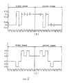
- FIGS 2 (a) and 2 (b) Exemplary voltage wave forms according to the two correction modes are shown in Figures 2 (a) and 2 (b).
- a scanning voltage wave form impressed on the scanning electrode Y4 when the liquid crystal panel shows the display of Figure 1 is indicated in Figure 2 (a)
- a signalling voltage wave form impressed on the signalling electrode X5 is indicated in Figure 2 (b)
- a voltage wave form indicated in Figure 2 (a) by a broken line represents a disturbance of the wave form applied to the scanning electrode Y4 arising at a position of the signalling electrode X5.
- the ordinate indicates voltage
- the abscissa indicates time.
- VO, V1U, V1, V1L, V2, V3, V4U, V4, V4L, V5 each represent voltage values.
- Voltages V0 and V4 in the scanning voltage wave form are a selection voltage and a non-selection voltage, respectively, of a first set of such voltages
- voltages V5 and V1 are a selection voltage and a non-selection voltage, respectively, of a second set of such voltages.
- voltages V5 and V3 in the signalling voltage wave form are a lighting voltage and a non-lighting voltage, respectively, in a first set of such voltages
- voltages V0 and V2 are a lighting voltage and a non-lighting voltage, respectively, is a second set of such voltages.
- Each of the two sets of selection and non-selection, and lighting and non-lighting, voltages are changed cyclically, thus keeping a DC voltage from being applied to the liquid crystal panel.
- each driving voltage is generated by the first sets of the voltages while the scanning electrodes Y1 to Y5 in the first frame are selected, is generated by the second sets of the voltages while the scanning electrodes Y6 to Y10 in the first frame and the scanning electrodes Y1 to Y5 in the second frame consecutive thereto are selected, and is generated again by the first sets of the voltage while the scanning electrodes Y6 to Y10 in the second frame are selected.
- the first voltage set and the second voltage set replace one another, and each driving wave form is generated by the second sets of the voltages while the scanning electrodes Y1 to Y5 in the first frame are selected, is generated by the first sets of the voltages while the scanning electrodes Y6 to Y10 in the first frame and the scanning electrodes Y1 to Y5 in the second frame consecutive thereto are selected, and is generated again by the second sets of the voltages while the scanning electrodes Y6 to Y10 in the second frame are selected.
- the above process is then repeated.
- the state reverts in two periods (four frames) to prevent a DC voltage from being applied to the liquid crystal panel, and is not therefore of substantial duration.
- the change of state is not necessarily limited to the above, and an arbitrary number of changes and an arbitrary time interval may be employed, if necessary, before the state reverts so long as a DC voltage is not applied to the liquid crystal panel.
- the numeric values which are not parenthesised are effective. That is, when the selected scanning electrode is changed, if the first voltage set and the second voltage set do not change over (herein-after referred to as the polarity not being inverted), a correction is applied according to the difference I, but if they do change (hereinafter referred to as the polarity being inverted), then a correction is applied according to the numeric value F.
- the correction voltages (V4L, V1U) tending towards the lighting voltage, or the correction voltages (V4U, V1L) tending towards the non-lighting voltage are impressed on each of the scanning electrodes Y1 to Y10, instead of the non-selection voltage, according to whether the difference I is positive or negative for a time corresponding to the absolute value of the difference I, thereby substantially off setting such disturbance of the wave form.
- a disturbance of the scanning voltage wave form according to the absolute value of the numeric value F may arise tending towards the lighting or the non-lighting voltage according to whether the numeric value F is positive or negative.
- the correction voltages (V4U, V1L) tending towards the non-lighting voltage, or the correction voltages (V4L, V1U) tending towards the lighting voltage are applied to each of the scanning electrodes Y1 to Y10, instead of the non-selection voltage, according to whether the numeric value F is positive or negative for a time corresponding to the absolute value of the numeric value F, thereby off setting the disturbance of the wave forms.
- the wave form at any of the display dots within the liquid crystal panel in practice has correction voltages, countering a disturbance arising in the wave form, applied thereto for a time corresponding to the magnitude of the disturbance. Therefore, the disturbance is substantially off set by the correction voltages.
- the effective voltage applied to the display dots will be substantially corrected and a tone display free from uneveness will be obtainable.
- a tone display is effected by lighting a display dot in one frame of the period and not lighting it in the next frame to cause flickering.
- a depth of half the full tone may be obtained.
- Figure 3 is illustrative thereof.
- Figures 3 (a), 3 (b) and 3 (c) show display patterns in first, second and third frames, respectively, in the same liquid crystal panel as Figure 1.
- a square is displayed centrally.
- the display dots on the scanning electrodes (Y3, Y6), whose number is divisible by three, and the scanning electrodes (Y4, Y7) whose number divided by three leaves a remainder of one, are lit.
- the display dots on the scanning electrodes (Y4, Y7), whose number divided by three leaves a remainder of one, and the scanning electrodes (Y5, Y8), whose number divided by three leaves a remainder of two, are lit.
- the display dots on the scanning electrodes (Y3, Y6) whose number is divisible by three, and the scanning electrodes (Y5, Y8), whose number divided by three leaves a remainder of two, are lit.
- the method employed for tone display here with the three frames constituting one period again causes all the display dots on each respective scanning electrode to flicker in phase irrespective of the positions of the signalling electrodes.
- a correction voltage is superposed on the scanning voltage wave form or on the signalling voltage wave form according to the difference I, and a correction voltage is superposed on the scanning voltage wave form or on the signalling voltage wave form according to the numeric value F, in order to correct an effective voltage applied to the display dots substantially as in the case of Example 1.
- a tone display free from uneveness is obtainable in consequence.
- Example 1 With the three frames in one period, the display dots are lit in two frames within one period, and therefore two thirds of the full tone will be obtained in this case. Accordingly, a tone somewhat deeper than Example 1 is obtainable.
- the number of frames in one period may be properly set, and the number of times the dots are lit within the one period may be adjusted, so as to realise an arbitrary tone display without producing uneveness. Needless to say, a plurality of different tones may be displayed concurrently.
- uneveness in a display arising in the prior art when the first known display method is carried out may be prevented by changing the wave form for driving a liquid crystal panel according to the display pattern required on the liquid crystal panel.
- a driving method for effecting a tone display free from uneveness may be provided.
Abstract
Description
- The present invention relates to a method for driving a liquid crystal panel.
- A driving method, known as a voltage averaging method, has generally been employed hitherto for driving a matrix type liquid crystal panel having a plurality of scanning electrodes and a plurality of signalling electrodes intersecting one another to form a dot matrix. In this method, a selection voltage is applied successively to all the scanning electrodes during "one frame" (the scanning electrodes to which a selection voltage is applied are called "selected" here-inafter). A lighting voltage or a non-lighting voltage is applied to respective signalling electrodes synchronously therewith. The process is cyclically repeated. Thus, each dot of a display pattern is lit or is not lit to create a display. A plurality of frames are defined as one period. The frequency for lighting or not lighting each display dot is cyclically changed every frame for realising tones in the grey scale.
- A driving method is also known in which the polarity of the voltages impressed on the liquid crystal panel is periodically inverted so as to avoid applying a DC voltage to the liquid crystal panel.
- In particular, a method (called a first method) is well known in which the phase with which each display dot on any respective scanning electrode flickers on and off is made the same irrespective of the positions of the associated signalling electrodes. A further method (called a second method) is also well known in which the phase with which each display dot on any respective scanning electrode flickers on and off is varied according to the position of the associated signalling electrode.
- The first method will be described with reference to Figures 1 (a) and 1 (b). Figures 1 (a) and 1 (b) are views showing typical display contents of the same liquid crystal panel in a first frame and a second frame, respectively. In Figure 1, the references Y1 to Y10 represent the scanning electrodes, and the references X1 to X10 represent the signalling electrodes. Points where the scanning electrodes Y1 to Y10 and the signalling electrodes X1 to X10 intersect each other function to provide display dots for creating a display, a mark o representing a non-lit dot and a mark ● representing a lit dot. The scanning electrodes Y1 to Y10 are selected in the order Y1 to Y10. In this example, a square is displayed as a half tone image in the centre of the panel.
- As illustrated, display dots on the odd numbered scanning electrodes (Y3, Y5, Y7) are not lit in the first frame and are lit in the second frame, thus flickering, so understood, with the same phase irrespective of the positions of the signalling electrodes X1 to X10 associated with those display dots. Similarly, the display dots on the even numbered scanning electrodes (Y4, Y6, Y8) are lit in the first frame, but are not lit in the second frame, again flickering with the same phase. Thus, the first method equalises the phase of the flickering cycle of all the display dots on each scanning electrode irrespective of the positions of the corresponding signalling electrodes.
- Next, the second method will be described with reference to Figures 4 (a) and 4 (b). Figures 4 (a) and 4 (b) show typical display contents of the same liquid crystal panel in a first frame and a second frame, respectively. The features of this panel other than the display contents are the same as in Figure 1 and, therefore, a further description will be omitted.
- As illustrated in Figure 4, the display dots provided by the odd numbered scanning electrodes (Y3, Y5, Y7) and the odd numbered signalling electrodes (X3, X5, X7), and the display dots provided by the even numbered scanning electrodes (Y4, Y6, Y8) and the even numbered signalling electrodes (X4, X6, X8) are not lit in the first frame, but are lit in the second frame. By contrast, the display dots provided by the even numbered scanning electrodes (Y4, Y6, Y8) and the even numbered signalling electrodes (X4, X6, X8), and the display dots provided by the odd numbered scanning electrodes (Y3, Y5, Y7) and the odd numbered signalling electrodes (X3, X5, X7) are not lit in the first frame, but are lit in the second frame, thus flickering, so understood, with different phases according to the position of the associated signalling electrode (the number of such signalling electrode). The second method, therefore, varies the phase of the flickering cycles of the display dots provided on the scanning electrodes according to the position of the signalling electrodes.
- The first method is described in Japanese Patent Application No. 63-159914 (European Patent Application No. 88307505.3). However, a problem arises with the first method in that, when the selected scanning electrodes are changed successively, uneveness arises in the display (cross talk arises when displaying a "zebra" pattern) according to a difference I in the number of the display dots lit on a selected scanning electrode and the number of dots to be lit on the scanning electrode which is to be selected next. In general, when the selected scanning electrode changes from the nth scanning electrode to the (n + 1)th scanning electrode, if the number of lit dots on the nth scanning electrode is NON and the number of lit dots on the (n + 1)th scanning electrode is MON, and if the difference I obtained (I = NON - MON ) is negative, then a spike voltage tending towards the level of the lighting voltage is generated on each scanning electrode according to the absolute value of the difference I. When the difference I is positive, a spike voltage tending towards the level of the non-lighting voltage is generated according to the absolute value of the difference I.
- Accordingly, when the selected scanning electrode shifts successively, then, for so long as the difference I has a substantial absolute value, considerable uneveness arises in the effective voltage applied to the display dots due to the spike voltage, thus promoting uneveness of the display.
- For example, when a display is effected according to the first method represented in Figure 1 and all the display dots on each scanning electrode are lit, or not lit, at once in each frame, then as the selection shifts from the scanning electrode Y3 through to the scanning electrode Y8, a big difference I is generated. By way of example, the difference I is 6 when the scanning electrode is changed from Y4 to Y5. Consequently, considerable uneveness in the display unavoidably results.
- In the second method represented in Figure 4, the difference in the number of lit dots from one selected scanning electrode to the next is minimised (nil, for example, when the selected scanning electrode changes from Y4 to Y5), thereby making it possible to avoid uneveness in the display. That is, the construction is such that a charge and discharge rate for the electric charge for the display dots provided on some selected scanning electrode and each odd numbered signalling electrode is equal to a charge and discharge rate for the electric charge for display dots provided on the selected scanning electrode and each even numbered signalling electrode.
- However, in the case of a colour liquid crystal panel having a filter of three colours or more, where signalling electrodes are disposed very close together, there may be a case where an element for supplying a driving wave form to the signalling electrodes cannot be connected to the same end of all the signalling electrodes, and must consequently be connected alternately to the opposite ends (the upper and lower ends as shown) of the signalling electrodes to moderate the connection density. However, in Figure 4, when the driving wave form is applied, for example, to the odd numbered signalling electrodes (X1, X3, X5, X7, X9) from above, and the driving wave form is applied to the even numbered signalling electrodes (X2, X4, X6, X8, X10) from below, there will then arise a uneveness in the display carried out according to the second method, as before.
- While a detailed description will be omitted here, when a grey scale tone display is provided according to the second method, for example, on an upper portion of the liquid crystal panel, a charge and discharge rate for the electric charge for the display dots provided by the odd numbered signalling electrodes with the driving wave form applied thereto from above is greater than a charge and discharge rate for the electric charge for the display dots provided by the even numbered signalling electrodes with the driving wave form applied thereto from below. The reason for the difference is that since the driving wave form is applied to the even numbered signalling electrodes from below, i.e. remote from the display dots present on the upper side, it is severely attenuated by resistance of the signalling electrodes and other factors. And since the odd numbered signalling electrodes have the driving wave form applied thereto from above, the driving wave form on the signalling electrodes at the position of the display is scarcely attenuated. The driving wave form is thus distorted and a difference in the charge and discharge rate occurs, leading to a uneveness in the display.
- In addition, uneveness may also be caused in a display for a further reason (polarity inversion cross talk). In this instance, when the polarity of the voltage impressed on the liquid crystal panel is inverted when the selected scanning electrode is changed, a disruption of the wave form according to a numeric value F, obtained through deducting the full number of display dots on each scanning electrode (namely the number of signalling electrodes) from the sum of the number of lit dots on the selected scanning electrode and the number of dots to be lit on the scanning electrode selected next, may arise on each scanning electrode.
- When the numeric value F is negative, a rounding according to the absolute value of the numeric value F arises in the voltage wave form on each scanning electrode immediately after the selection is changed. When the numeric value F is positive, a spike voltage having a magnitude according to the absolute value of the numeric value F is generated tending towards the value of the lighting voltage. A substantial uneveness thus arises in the effective voltage applied to the display dots due to the waveform disruption, thus causing uneveness in the display.
- The quality of a display on a liquid crystal panel is severely impaired by the uneveness.
- It is an object of the present invention to provide a driving method for effecting a grey scale tone display free from such uneveness as are described above.
- According to the present invention, there is provided a method for driving a liquid crystal panel having a plurality of scanning electrodes and a plurality of signalling electrodes intersecting one another to form a dot matrix, the method comprising applying a driving voltage to each dot of a display pattern such that each said display dot is lit or is not lit in every frame of a display period with the frequency of lighting or not lighting each display dot being varied cyclically within the display period for generating a grey scale tone display, and characterised by controlling the application of the driving voltage such that a plurality of the said display dots on each scanning electrode are lit or not lit in phase with one another, and applying a correction to the driving voltage determined according to the form of the display pattern for off setting disturbances generated in the driving voltage.
- The display pattern itself may be a character, a graphic form or the like.
- By means of the present invention, uneveness in a display due to stringing every other piece or polarity inversion may be prevented.
- The present invention will be described further, by way of example, with reference to the accompanying drawings, in which:
- Figures 1 (a) and 1 (b) are views of a liquid crystal panel to which a first embodiment of the present invention may be applied and illustrating display contents thereof;
- Figures 2 (a) and 2 (b) are views showing driving wave forms in the first embodiment of the present invention;
- Figures 3 (a) to 3 (c) are views of a liquid crystal panel to which a second embodiment of the present invention may be applied and illustrating display contents thereof; and
- Figures 4 (a) and 4 (b) are views of a liquid crystal panel driven according to the prior art and illustrating display contents thereof.
- Figures 1 (a) and 1 (b) show a liquid crystal panel and its display patterns in a first frame and a second frame, respectively. The liquid crystal panel is shown diagrammatically with the references Y1 to Y10 representing scanning electrodes, and the references X1 to X10 representing signalling electrodes. In practice, the panel has a pair of substrates holding a liquid crystal therebetween, and the scanning electrodes Y1 to Y10 are formed on one of the substrates and the signalling electrodes X1 to X10 are formed on the other substrate. The scanning electrodes Y1 to Y10 and the signalling electrodes X1 to X10 as shown are limited to only ten each. However, this is to simplify the description, and a far greater number will be provided in practice. Locations where the scanning electrodes Y1 to Y10 and the signalling electrodes X1 to X10 intersect each other function to form display dots for creating a display, the display dots designated by the mark o being non-lit dots, and the display dots designated by the mark ● being lit dots. In this example, a square is displayed by a half tone image centrally of the panel (namely, the square defined by the scanning electrodes Y3 to Y8 and the signalling electrodes X3 to X8). As illustrated, the display dots on the odd numbered scanning electrodes (Y3, Y5, Y7) are not lit in the first frame but are lit in the second frame, and the display dots on the even numbered scanning electrodes (Y4, Y6, Y8) are lit in the first frame but not lit in the second frame, in both cases flickering on and off in phase with one another. However, according to the invention, this driving method for realising a tone display, in which two frames constitute one period and in which all the display dots on each respective scanning electrode flicker on and off in phase with one another irrespective of the positions of the associated signalling electrodes, is modified by superposing a correction voltage on the driving wave form impressed on the scanning electrodes Y1 to Y10 (hereinafter called the scanning voltage wave form) or on the driving wave form impressed on the signalling electrodes X1 to X10 (hereinafter called the signalling voltage wave form).
- In the present embodiment, a constant correction voltage is applied to the scanning electrode during the time when it is not receiving the selection voltage (i.e. it is receiving a non-selection voltage) for a duration corresponding to the difference I (mentioned previously). Accordingly, when the difference I is negative, in the case where the polarity of the voltage impressed on the liquid crystal panel is not inverted when the selected scanning electrode is changed, correction voltages (V4U, V1L) having values between the non-selecting voltage and the non-lighting voltage are applied to each scanning electrode instead of the non-selection voltage for a time corresponding to an absolute value of the difference I. When the difference I is positive, the correction voltages (V4L, V1U) having values between the non-selection voltage and the lighting voltage are applied to each scanning electrode instead of the non-selection voltage for a time corresponding to the absolute value of the difference I.
- Further, in the case where the polarity of the driving voltage impressed on the liquid crystal panel is inverted when the selected scanning electrode is changed from Yn to Yn + 1, a correction voltage is superposed on the scanning voltage wave form applied to the scanning electrodes Y1 to Y10, or on the signalling voltage wave form applied to the signalling electrodes X1 to X10, according to a value F obtained through deducting the number of signalling electrodes X1 to X10 from the sum of the number of lit dots on the selected scanning electrode Yn and the number of lit dots on the selected scanning
electrode Yn + 1. - In the present embodiment, a constant correction voltage is applied to the scanning electrode instead of the non-selection voltage for a time corresponding to the numeric value F. Accordingly, when the numeric value F is positive, in the case where the polarity of the voltage impressed on the liquid crystal panel is inverted when the selected scanning electrode is changed, the correction voltages (V4U, V1L) having values between the non-selection voltage and the non-lighting voltage are applied to each scanning electrode instead of the non-selection voltage for a time corresponding to the absolute value of the numeric value F and, when the numeric value F is positive, the correction voltages (V4L, V1U) having values between the non-selection voltage and the lighting voltage are applied to each scanning electrode instead of the non-selection voltage for a time corresponding to the absolute value of the numeric value F.
- These two modes of correction, in which the driving wave form applied to the liquid crystal panel is modified, are both used together. Exemplary voltage wave forms according to the two correction modes are shown in Figures 2 (a) and 2 (b). A scanning voltage wave form impressed on the scanning electrode Y4 when the liquid crystal panel shows the display of Figure 1 is indicated in Figure 2 (a), and a signalling voltage wave form impressed on the signalling electrode X5 is indicated in Figure 2 (b), by a full line each. A voltage wave form indicated in Figure 2 (a) by a broken line represents a disturbance of the wave form applied to the scanning electrode Y4 arising at a position of the signalling electrode X5. The ordinate indicates voltage, and the abscissa indicates time. On the ordinate, VO, V1U, V1, V1L, V2, V3, V4U, V4, V4L, V5 each represent voltage values. Voltages V0 and V4 in the scanning voltage wave form are a selection voltage and a non-selection voltage, respectively, of a first set of such voltages, and voltages V5 and V1 are a selection voltage and a non-selection voltage, respectively, of a second set of such voltages. Similarly, voltages V5 and V3 in the signalling voltage wave form are a lighting voltage and a non-lighting voltage, respectively, in a first set of such voltages, and voltages V0 and V2 are a lighting voltage and a non-lighting voltage, respectively, is a second set of such voltages. Then, voltages V1U, V1L and V4U, V4L are correction voltages applied in place of the non-selection voltages V1 and V4. = V0 - V1
Here, V
= V1 - V2
= V3 - V4
= V4 - V5
= a (V1U - V1)
= b (V1 - V1L)
= b (V4U - V4)
= a (V4 - V4L)
where a, b, ≧ 1. - Each of the two sets of selection and non-selection, and lighting and non-lighting, voltages are changed cyclically, thus keeping a DC voltage from being applied to the liquid crystal panel.
- In the present embodiment, during one period consisting of the first frame and the second frame, each driving voltage is generated by the first sets of the voltages while the scanning electrodes Y1 to Y5 in the first frame are selected, is generated by the second sets of the voltages while the scanning electrodes Y6 to Y10 in the first frame and the scanning electrodes Y1 to Y5 in the second frame consecutive thereto are selected, and is generated again by the first sets of the voltage while the scanning electrodes Y6 to Y10 in the second frame are selected. Then, in the next period (not indicated) the first voltage set and the second voltage set replace one another, and each driving wave form is generated by the second sets of the voltages while the scanning electrodes Y1 to Y5 in the first frame are selected, is generated by the first sets of the voltages while the scanning electrodes Y6 to Y10 in the first frame and the scanning electrodes Y1 to Y5 in the second frame consecutive thereto are selected, and is generated again by the second sets of the voltages while the scanning electrodes Y6 to Y10 in the second frame are selected. The above process is then repeated.
- Here, the state reverts in two periods (four frames) to prevent a DC voltage from being applied to the liquid crystal panel, and is not therefore of substantial duration. However, the change of state is not necessarily limited to the above, and an arbitrary number of changes and an arbitrary time interval may be employed, if necessary, before the state reverts so long as a DC voltage is not applied to the liquid crystal panel.
- In Figures 2 (a) and 2 (b), the duration of each of the first frame and the second frame are shown. Further, the references T1 to T10 indicate the time in which each of the scanning electrodes Y1 to Y10 is respectively selected.
- From Figure 1, the difference I and the numeric value F when the selection in every frame is changed will be as follows:
In the first frame:
When the selection is changed from the scanning electrode Y1 to the scanning electrode Y2:

When the selection is changed from the scanning electrode Y2 to the scanning electrode Y3:

When the selection is changed from the scanning electrode Y3 to the scanning electrode Y4:

When the selection is changed from the scanning electrode Y4 to the scanning electrode Y5:

When the selection is changed from the scanning electrode Y5 to the scanning electrode Y6:

When the selection is changed from the scanning electrode Y6 to the scanning electrode Y7:

When the selection is changed from the scanning electrode Y7 to the scanning electrode Y8:

When the selection is changed from the scanning electrode Y8 to the scanning electrode Y9:

When the selection is changed from the scanning electrode Y9 to the scanning electrode Y10:

When the selection is changed from the scanning electrode Y10 in the first frame to the scanning electrode Y1 in the second frame:

Next, in the second frame:
When the selection is changed from the scanning electrode Y1 to the scanning electrode Y2:

When the selection is changed from the scanning electrode Y2 to the scanning electrode Y3:

When the selection is changed from the scanning electrode Y3 to the scanning electrode Y4:

When the selection is changed from the scanning electrode Y4 to the scanning electrode Y5:

When the selection is changed from the scanning electrode Y5 to the scanning electrode Y6:

When the selection is changed from the scanning electrode Y6 to the scanning electrode Y7:

When the selection is changed from the scanning electrode Y7 to the scanning electrode Y8:

When the selection is changed from the scanning electrode Y8 to the scanning electrode Y9:

When the selection is changed from the scanning electrode Y9 to the scanning electrode Y10:

When the selection is changed from the scanning electrode Y10 in the second frame to the scanning electrode Y1 in the first frame:

- Here, the numeric values which are not parenthesised are effective. That is, when the selected scanning electrode is changed, if the first voltage set and the second voltage set do not change over (herein-after referred to as the polarity not being inverted), a correction is applied according to the difference I, but if they do change (hereinafter referred to as the polarity being inverted), then a correction is applied according to the numeric value F.
- Accordingly, when a selected scanning electrode is changed where the polarity is not inverted, as indicated by broken lines covering the times T4 to T5, T6 to T7, T7 to T8, T8 to T9 of each frame of Figure 2 (a), a non-lighting voltage according to whether the difference I is positive or negative will be generated, and a disturbance in the form of a spike voltage corresponding to an absolute value of the difference I tending towards the lighting voltage may arise in the non-selection voltage. However, as indicated by the full line in Figure 2 (a), the correction voltages (V4L, V1U) tending towards the lighting voltage, or the correction voltages (V4U, V1L) tending towards the non-lighting voltage, are impressed on each of the scanning electrodes Y1 to Y10, instead of the non-selection voltage, according to whether the difference I is positive or negative for a time corresponding to the absolute value of the difference I, thereby substantially off setting such disturbance of the wave form.
- Similarly, where the polarity is inverted, as indicated by broken lines covering the times T1 of the first frame and T5 to T6 of each frame, a disturbance of the scanning voltage wave form according to the absolute value of the numeric value F may arise tending towards the lighting or the non-lighting voltage according to whether the numeric value F is positive or negative. However, as indicated by the full line of Figure 2 (a), the correction voltages (V4U, V1L) tending towards the non-lighting voltage, or the correction voltages (V4L, V1U) tending towards the lighting voltage, are applied to each of the scanning electrodes Y1 to Y10, instead of the non-selection voltage, according to whether the numeric value F is positive or negative for a time corresponding to the absolute value of the numeric value F, thereby off setting the disturbance of the wave forms.
- Thus, the scanning voltage wave form with the correction voltage is applied thereto as indicated by the full line of Figure 2 (a) is formed according to the difference I and the numeric value F.
- As described, the wave form at any of the display dots within the liquid crystal panel in practice has correction voltages, countering a disturbance arising in the wave form, applied thereto for a time corresponding to the magnitude of the disturbance. Therefore, the disturbance is substantially off set by the correction voltages. Thus, the effective voltage applied to the display dots will be substantially corrected and a tone display free from uneveness will be obtainable.
- In the above example, having two frames in one period, a tone display is effected by lighting a display dot in one frame of the period and not lighting it in the next frame to cause flickering. When expressed by a value obtained by dividing the number of times of lighting the dot by the number of frames in one period, it may be seen that a depth of half the full tone may be obtained. However, not only half the tone but also various other depths of tone may be realised by the present invention. Figure 3 is illustrative thereof.
- Figures 3 (a), 3 (b) and 3 (c) show display patterns in first, second and third frames, respectively, in the same liquid crystal panel as Figure 1. As illustrated, a square is displayed centrally. In the first frame, the display dots on the scanning electrodes (Y3, Y6), whose number is divisible by three, and the scanning electrodes (Y4, Y7) whose number divided by three leaves a remainder of one, are lit. Then, in the second frame, the display dots on the scanning electrodes (Y4, Y7), whose number divided by three leaves a remainder of one, and the scanning electrodes (Y5, Y8), whose number divided by three leaves a remainder of two, are lit. Further, in the third frame, the display dots on the scanning electrodes (Y3, Y6) whose number is divisible by three, and the scanning electrodes (Y5, Y8), whose number divided by three leaves a remainder of two, are lit.
- Thus, the method employed for tone display here with the three frames constituting one period again causes all the display dots on each respective scanning electrode to flicker in phase irrespective of the positions of the signalling electrodes. At the same time, a correction voltage is superposed on the scanning voltage wave form or on the signalling voltage wave form according to the difference I, and a correction voltage is superposed on the scanning voltage wave form or on the signalling voltage wave form according to the numeric value F, in order to correct an effective voltage applied to the display dots substantially as in the case of Example 1. A tone display free from uneveness is obtainable in consequence.
- With the three frames in one period, the display dots are lit in two frames within one period, and therefore two thirds of the full tone will be obtained in this case. Accordingly, a tone somewhat deeper than Example 1 is obtainable.
- As described above, with the phase of the flickering cycles of all the display dots on a scanning electrode being the same, then according to the invention the number of frames in one period may be properly set, and the number of times the dots are lit within the one period may be adjusted, so as to realise an arbitrary tone display without producing uneveness. Needless to say, a plurality of different tones may be displayed concurrently.
- In the above described Examples, while constant correction voltages are applied for a time corresponding to the difference I and the numeric value F, a similar effect will be obtainable from using a variable correction voltage according to the difference I and the numeric value F, e.g. as described in Japanese Patent Application No. 63-159914.
- According to the present invention, uneveness in a display arising in the prior art when the first known display method is carried out may be prevented by changing the wave form for driving a liquid crystal panel according to the display pattern required on the liquid crystal panel. Thus, a driving method for effecting a tone display free from uneveness may be provided.
Claims (8)
- A method for driving a liquid crystal panel having a plurality of scanning electrodes (Y1 to Y10) and a plurality of signalling electrodes (X1 to X10) intersecting one another to form a dot matrix, the method comprising applying a driving voltage to each dot of a display pattern such that each said display dot is lit or is not lit in every frame of a display period with the frequency of lighting or not lighting each display dot being varied cyclically within the display period for generating a grey scale tone display, and characterised by controlling the application of the driving voltage such that a plurality of the said display dots on each scanning electrode are lit or not lit in phase with one another, and applying a correction to the driving voltage determined according to the form of the display pattern for off setting disturbances generated in the driving voltage.
- A method according to claim 1 characterised in that the step of applying the correction comprises applying a constant correction voltage to the driving voltage for a duration determined according to the form of the display pattern.
- A method according to claim 1 or 2 characterised in that the correction is determined according to the difference in the number of display dots lit on successively selected scanning electrodes.
- A method according to any of claims 1 to 3 characterised in that the correction is determined according to the sum of the display dots lit on successively selected scanning electrodes minus the total number of dots available on any scanning electrode.
- A method according to any of claims 1 to 4 characterised in that a respective scanning voltage wave form is applied to each scanning electrode for generating the driving voltage, and in that the correction is applied to the scanning voltage wave form.
- A method according to claim 5 characterised in that the correction is applied to a non-selection voltage of the scanning voltage wave form.
- A method according to any of claims 1 to 4 characterised in that a respective signalling voltage wave form is applied to each signalling electrode for generating the driving voltage, and in that the correction is applied to the signalling voltage wave form.
- In a driving method for a liquid crystal panel, wherein each of a plurality of display dots of a liquid crystal panel of a dot matrix with said display dots constructed of a plurality of scanning electrodes (Y1 to Y10) and a plurality of signalling electrodes (X1 to X10) intersecting each other is lighted or kept from lighting at every frame, and with a term consisting of said frames as one period, a frequency of lighting or keeping from lighting said each display dot cyclically within the one period is changed to a tone display, characterised in that phases of cycles for lighting or non-lighting of said each display dot within said one period are equalised at every display dot on said each scanning electrode, a driving wave form of said liquid crystal panel is changed according to a display pattern such as character, graphic form or the like displayed by said liquid crystal panel.
Applications Claiming Priority (2)
| Application Number | Priority Date | Filing Date | Title |
|---|---|---|---|
| JP2641590A JPH03231286A (en) | 1990-02-06 | 1990-02-06 | Driving method for liquid crystal panel |
| JP26415/90 | 1990-02-06 |
Publications (3)
| Publication Number | Publication Date |
|---|---|
| EP0441591A2 true EP0441591A2 (en) | 1991-08-14 |
| EP0441591A3 EP0441591A3 (en) | 1992-12-23 |
| EP0441591B1 EP0441591B1 (en) | 1998-06-10 |
Family
ID=12192913
Family Applications (1)
| Application Number | Title | Priority Date | Filing Date |
|---|---|---|---|
| EP19910300930 Expired - Lifetime EP0441591B1 (en) | 1990-02-06 | 1991-02-05 | A method for driving a liquid crystal panel |
Country Status (3)
| Country | Link |
|---|---|
| EP (1) | EP0441591B1 (en) |
| JP (1) | JPH03231286A (en) |
| DE (1) | DE69129553T2 (en) |
Cited By (3)
| Publication number | Priority date | Publication date | Assignee | Title |
|---|---|---|---|---|
| EP0612184A2 (en) * | 1993-02-19 | 1994-08-24 | Asahi Glass Company Ltd. | Display apparatus and a data signal forming method for the display apparatus |
| US6542141B1 (en) | 1991-10-01 | 2003-04-01 | Hitachi, Ltd. | Liquid-crystal halftone display system |
| SG111019A1 (en) * | 2000-07-24 | 2005-05-30 | Seiko Epson Corp | Driving method for electro-optical apparatus, driving circuit therefor, electro-optical apparatus, and electronic equipment |
Citations (3)
| Publication number | Priority date | Publication date | Assignee | Title |
|---|---|---|---|---|
| EP0303510A2 (en) * | 1987-08-13 | 1989-02-15 | Seiko Epson Corporation | Liquid crystal display device |
| US4808991A (en) * | 1986-01-13 | 1989-02-28 | Hitachi, Ltd. | Method and apparatus for liquid crystal display with intermediate tone |
| DE3906924A1 (en) * | 1988-03-05 | 1989-09-14 | Sharp Kk | Grey-scale imaging method having a pixel-matrix display device |
-
1990
- 1990-02-06 JP JP2641590A patent/JPH03231286A/en active Pending
-
1991
- 1991-02-05 EP EP19910300930 patent/EP0441591B1/en not_active Expired - Lifetime
- 1991-02-05 DE DE1991629553 patent/DE69129553T2/en not_active Expired - Fee Related
Patent Citations (3)
| Publication number | Priority date | Publication date | Assignee | Title |
|---|---|---|---|---|
| US4808991A (en) * | 1986-01-13 | 1989-02-28 | Hitachi, Ltd. | Method and apparatus for liquid crystal display with intermediate tone |
| EP0303510A2 (en) * | 1987-08-13 | 1989-02-15 | Seiko Epson Corporation | Liquid crystal display device |
| DE3906924A1 (en) * | 1988-03-05 | 1989-09-14 | Sharp Kk | Grey-scale imaging method having a pixel-matrix display device |
Cited By (5)
| Publication number | Priority date | Publication date | Assignee | Title |
|---|---|---|---|---|
| US6542141B1 (en) | 1991-10-01 | 2003-04-01 | Hitachi, Ltd. | Liquid-crystal halftone display system |
| EP0612184A2 (en) * | 1993-02-19 | 1994-08-24 | Asahi Glass Company Ltd. | Display apparatus and a data signal forming method for the display apparatus |
| EP0612184A3 (en) * | 1993-02-19 | 1995-02-15 | Asahi Glass Co Ltd | Display apparatus and a data signal forming method for the display apparatus. |
| US5644329A (en) * | 1993-02-19 | 1997-07-01 | Asahi Glass Company Ltd. | Display apparatus and a data signal forming method for the display apparatus |
| SG111019A1 (en) * | 2000-07-24 | 2005-05-30 | Seiko Epson Corp | Driving method for electro-optical apparatus, driving circuit therefor, electro-optical apparatus, and electronic equipment |
Also Published As
| Publication number | Publication date |
|---|---|
| EP0441591B1 (en) | 1998-06-10 |
| EP0441591A3 (en) | 1992-12-23 |
| DE69129553D1 (en) | 1998-07-16 |
| JPH03231286A (en) | 1991-10-15 |
| DE69129553T2 (en) | 1999-03-25 |
Similar Documents
| Publication | Publication Date | Title |
|---|---|---|
| KR100343513B1 (en) | Liquid crystal driving method and apparatus | |
| TW346613B (en) | Liquid crystal display device and method for driving the same | |
| EP0953956B1 (en) | Light modulating device using a combination of spatial and temporal dithering techniques for grey levels generation | |
| US5119085A (en) | Driving method for a liquid crystal panel | |
| KR100378757B1 (en) | Gray shade driving device of liquid crystal display panel | |
| JP2005524860A (en) | Low power LCD with gradation drive system | |
| KR100501030B1 (en) | Method for driving simple matrix type el panel and simple matrix type el display device | |
| US5184118A (en) | Liquid crystal display apparatus and method of driving same | |
| EP0704087B1 (en) | A method of driving a picture display device | |
| KR19990029537A (en) | Liquid crystal display device and driving method of same device | |
| EP0441591B1 (en) | A method for driving a liquid crystal panel | |
| JP3875809B2 (en) | Driving method of liquid crystal display device | |
| KR19990023413A (en) | Simple matrix liquid crystal driving method | |
| JP2003121813A (en) | Method for driving gradations of liquid crystal panel | |
| JPH03130797A (en) | Display controller | |
| EP0438262B1 (en) | Method of driving a liquid crystal panel | |
| JP3074686B2 (en) | Driving method of liquid crystal panel | |
| EP0431628B1 (en) | Liquid crystal display device | |
| KR100343381B1 (en) | Liquid crystal display | |
| JPH04360192A (en) | Liquid crystal display device | |
| JPH1124043A (en) | Liquid crystal display device and its driving method | |
| KR100366085B1 (en) | Method for driving matrix type liquid crystal display | |
| JPS63240531A (en) | Liquid crystal display device | |
| JP3082765B2 (en) | Driving method of liquid crystal panel | |
| JP3632569B2 (en) | Method for driving liquid crystal device and display device |
Legal Events
| Date | Code | Title | Description |
|---|---|---|---|
| PUAI | Public reference made under article 153(3) epc to a published international application that has entered the european phase |
Free format text: ORIGINAL CODE: 0009012 |
|
| AK | Designated contracting states |
Kind code of ref document: A2 Designated state(s): DE FR GB |
|
| PUAL | Search report despatched |
Free format text: ORIGINAL CODE: 0009013 |
|
| AK | Designated contracting states |
Kind code of ref document: A3 Designated state(s): DE FR GB |
|
| 17P | Request for examination filed |
Effective date: 19930521 |
|
| 17Q | First examination report despatched |
Effective date: 19941024 |
|
| GRAG | Despatch of communication of intention to grant |
Free format text: ORIGINAL CODE: EPIDOS AGRA |
|
| GRAG | Despatch of communication of intention to grant |
Free format text: ORIGINAL CODE: EPIDOS AGRA |
|
| GRAG | Despatch of communication of intention to grant |
Free format text: ORIGINAL CODE: EPIDOS AGRA |
|
| GRAH | Despatch of communication of intention to grant a patent |
Free format text: ORIGINAL CODE: EPIDOS IGRA |
|
| GRAH | Despatch of communication of intention to grant a patent |
Free format text: ORIGINAL CODE: EPIDOS IGRA |
|
| GRAA | (expected) grant |
Free format text: ORIGINAL CODE: 0009210 |
|
| AK | Designated contracting states |
Kind code of ref document: B1 Designated state(s): DE FR GB |
|
| PG25 | Lapsed in a contracting state [announced via postgrant information from national office to epo] |
Ref country code: FR Free format text: LAPSE BECAUSE OF FAILURE TO SUBMIT A TRANSLATION OF THE DESCRIPTION OR TO PAY THE FEE WITHIN THE PRESCRIBED TIME-LIMIT Effective date: 19980610 |
|
| REF | Corresponds to: |
Ref document number: 69129553 Country of ref document: DE Date of ref document: 19980716 |
|
| EN | Fr: translation not filed | ||
| PLBE | No opposition filed within time limit |
Free format text: ORIGINAL CODE: 0009261 |
|
| STAA | Information on the status of an ep patent application or granted ep patent |
Free format text: STATUS: NO OPPOSITION FILED WITHIN TIME LIMIT |
|
| 26N | No opposition filed | ||
| REG | Reference to a national code |
Ref country code: GB Ref legal event code: IF02 |
|
| PGFP | Annual fee paid to national office [announced via postgrant information from national office to epo] |
Ref country code: DE Payment date: 20080131 Year of fee payment: 18 |
|
| PGFP | Annual fee paid to national office [announced via postgrant information from national office to epo] |
Ref country code: GB Payment date: 20090204 Year of fee payment: 19 |
|
| PG25 | Lapsed in a contracting state [announced via postgrant information from national office to epo] |
Ref country code: DE Free format text: LAPSE BECAUSE OF NON-PAYMENT OF DUE FEES Effective date: 20090901 |
|
| GBPC | Gb: european patent ceased through non-payment of renewal fee |
Effective date: 20100205 |
|
| PG25 | Lapsed in a contracting state [announced via postgrant information from national office to epo] |
Ref country code: GB Free format text: LAPSE BECAUSE OF NON-PAYMENT OF DUE FEES Effective date: 20100205 |