EP0440918A2 - Flame retardant, low dielectric constant microsphere filled laminate - Google Patents
Flame retardant, low dielectric constant microsphere filled laminate Download PDFInfo
- Publication number
- EP0440918A2 EP0440918A2 EP90123488A EP90123488A EP0440918A2 EP 0440918 A2 EP0440918 A2 EP 0440918A2 EP 90123488 A EP90123488 A EP 90123488A EP 90123488 A EP90123488 A EP 90123488A EP 0440918 A2 EP0440918 A2 EP 0440918A2
- Authority
- EP
- European Patent Office
- Prior art keywords
- microspheres
- prepreg
- recited
- filler
- prepreg material
- Prior art date
- Legal status (The legal status is an assumption and is not a legal conclusion. Google has not performed a legal analysis and makes no representation as to the accuracy of the status listed.)
- Withdrawn
Links
Images


Classifications
-
- C—CHEMISTRY; METALLURGY
- C08—ORGANIC MACROMOLECULAR COMPOUNDS; THEIR PREPARATION OR CHEMICAL WORKING-UP; COMPOSITIONS BASED THEREON
- C08K—Use of inorganic or non-macromolecular organic substances as compounding ingredients
- C08K7/00—Use of ingredients characterised by shape
- C08K7/22—Expanded, porous or hollow particles
- C08K7/24—Expanded, porous or hollow particles inorganic
-
- C—CHEMISTRY; METALLURGY
- C08—ORGANIC MACROMOLECULAR COMPOUNDS; THEIR PREPARATION OR CHEMICAL WORKING-UP; COMPOSITIONS BASED THEREON
- C08J—WORKING-UP; GENERAL PROCESSES OF COMPOUNDING; AFTER-TREATMENT NOT COVERED BY SUBCLASSES C08B, C08C, C08F, C08G or C08H
- C08J5/00—Manufacture of articles or shaped materials containing macromolecular substances
- C08J5/24—Impregnating materials with prepolymers which can be polymerised in situ, e.g. manufacture of prepregs
- C08J5/246—Impregnating materials with prepolymers which can be polymerised in situ, e.g. manufacture of prepregs using polymer based synthetic fibres
-
- C—CHEMISTRY; METALLURGY
- C08—ORGANIC MACROMOLECULAR COMPOUNDS; THEIR PREPARATION OR CHEMICAL WORKING-UP; COMPOSITIONS BASED THEREON
- C08J—WORKING-UP; GENERAL PROCESSES OF COMPOUNDING; AFTER-TREATMENT NOT COVERED BY SUBCLASSES C08B, C08C, C08F, C08G or C08H
- C08J5/00—Manufacture of articles or shaped materials containing macromolecular substances
- C08J5/24—Impregnating materials with prepolymers which can be polymerised in situ, e.g. manufacture of prepregs
- C08J5/248—Impregnating materials with prepolymers which can be polymerised in situ, e.g. manufacture of prepregs using pre-treated fibres
-
- C—CHEMISTRY; METALLURGY
- C08—ORGANIC MACROMOLECULAR COMPOUNDS; THEIR PREPARATION OR CHEMICAL WORKING-UP; COMPOSITIONS BASED THEREON
- C08J—WORKING-UP; GENERAL PROCESSES OF COMPOUNDING; AFTER-TREATMENT NOT COVERED BY SUBCLASSES C08B, C08C, C08F, C08G or C08H
- C08J5/00—Manufacture of articles or shaped materials containing macromolecular substances
- C08J5/24—Impregnating materials with prepolymers which can be polymerised in situ, e.g. manufacture of prepregs
- C08J5/249—Impregnating materials with prepolymers which can be polymerised in situ, e.g. manufacture of prepregs characterised by the additives used in the prepolymer mixture
-
- H—ELECTRICITY
- H05—ELECTRIC TECHNIQUES NOT OTHERWISE PROVIDED FOR
- H05K—PRINTED CIRCUITS; CASINGS OR CONSTRUCTIONAL DETAILS OF ELECTRIC APPARATUS; MANUFACTURE OF ASSEMBLAGES OF ELECTRICAL COMPONENTS
- H05K1/00—Printed circuits
- H05K1/02—Details
- H05K1/03—Use of materials for the substrate
- H05K1/0313—Organic insulating material
- H05K1/0353—Organic insulating material consisting of two or more materials, e.g. two or more polymers, polymer + filler, + reinforcement
- H05K1/0373—Organic insulating material consisting of two or more materials, e.g. two or more polymers, polymer + filler, + reinforcement containing additives, e.g. fillers
-
- H—ELECTRICITY
- H05—ELECTRIC TECHNIQUES NOT OTHERWISE PROVIDED FOR
- H05K—PRINTED CIRCUITS; CASINGS OR CONSTRUCTIONAL DETAILS OF ELECTRIC APPARATUS; MANUFACTURE OF ASSEMBLAGES OF ELECTRICAL COMPONENTS
- H05K1/00—Printed circuits
- H05K1/02—Details
- H05K1/03—Use of materials for the substrate
- H05K1/0313—Organic insulating material
- H05K1/0353—Organic insulating material consisting of two or more materials, e.g. two or more polymers, polymer + filler, + reinforcement
- H05K1/0366—Organic insulating material consisting of two or more materials, e.g. two or more polymers, polymer + filler, + reinforcement reinforced, e.g. by fibres, fabrics
-
- H—ELECTRICITY
- H05—ELECTRIC TECHNIQUES NOT OTHERWISE PROVIDED FOR
- H05K—PRINTED CIRCUITS; CASINGS OR CONSTRUCTIONAL DETAILS OF ELECTRIC APPARATUS; MANUFACTURE OF ASSEMBLAGES OF ELECTRICAL COMPONENTS
- H05K2201/00—Indexing scheme relating to printed circuits covered by H05K1/00
- H05K2201/01—Dielectrics
- H05K2201/0104—Properties and characteristics in general
- H05K2201/012—Flame-retardant; Preventing of inflammation
-
- H—ELECTRICITY
- H05—ELECTRIC TECHNIQUES NOT OTHERWISE PROVIDED FOR
- H05K—PRINTED CIRCUITS; CASINGS OR CONSTRUCTIONAL DETAILS OF ELECTRIC APPARATUS; MANUFACTURE OF ASSEMBLAGES OF ELECTRICAL COMPONENTS
- H05K2201/00—Indexing scheme relating to printed circuits covered by H05K1/00
- H05K2201/02—Fillers; Particles; Fibers; Reinforcement materials
- H05K2201/0203—Fillers and particles
- H05K2201/0206—Materials
- H05K2201/0209—Inorganic, non-metallic particles
-
- H—ELECTRICITY
- H05—ELECTRIC TECHNIQUES NOT OTHERWISE PROVIDED FOR
- H05K—PRINTED CIRCUITS; CASINGS OR CONSTRUCTIONAL DETAILS OF ELECTRIC APPARATUS; MANUFACTURE OF ASSEMBLAGES OF ELECTRICAL COMPONENTS
- H05K2201/00—Indexing scheme relating to printed circuits covered by H05K1/00
- H05K2201/02—Fillers; Particles; Fibers; Reinforcement materials
- H05K2201/0203—Fillers and particles
- H05K2201/0206—Materials
- H05K2201/0239—Coupling agent for particles
-
- H—ELECTRICITY
- H05—ELECTRIC TECHNIQUES NOT OTHERWISE PROVIDED FOR
- H05K—PRINTED CIRCUITS; CASINGS OR CONSTRUCTIONAL DETAILS OF ELECTRIC APPARATUS; MANUFACTURE OF ASSEMBLAGES OF ELECTRICAL COMPONENTS
- H05K2201/00—Indexing scheme relating to printed circuits covered by H05K1/00
- H05K2201/02—Fillers; Particles; Fibers; Reinforcement materials
- H05K2201/0203—Fillers and particles
- H05K2201/0242—Shape of an individual particle
- H05K2201/0254—Microballoons or hollow filler particles
-
- H—ELECTRICITY
- H05—ELECTRIC TECHNIQUES NOT OTHERWISE PROVIDED FOR
- H05K—PRINTED CIRCUITS; CASINGS OR CONSTRUCTIONAL DETAILS OF ELECTRIC APPARATUS; MANUFACTURE OF ASSEMBLAGES OF ELECTRICAL COMPONENTS
- H05K2201/00—Indexing scheme relating to printed circuits covered by H05K1/00
- H05K2201/02—Fillers; Particles; Fibers; Reinforcement materials
- H05K2201/0275—Fibers and reinforcement materials
- H05K2201/029—Woven fibrous reinforcement or textile
-
- Y—GENERAL TAGGING OF NEW TECHNOLOGICAL DEVELOPMENTS; GENERAL TAGGING OF CROSS-SECTIONAL TECHNOLOGIES SPANNING OVER SEVERAL SECTIONS OF THE IPC; TECHNICAL SUBJECTS COVERED BY FORMER USPC CROSS-REFERENCE ART COLLECTIONS [XRACs] AND DIGESTS
- Y10—TECHNICAL SUBJECTS COVERED BY FORMER USPC
- Y10S—TECHNICAL SUBJECTS COVERED BY FORMER USPC CROSS-REFERENCE ART COLLECTIONS [XRACs] AND DIGESTS
- Y10S428/00—Stock material or miscellaneous articles
- Y10S428/901—Printed circuit
-
- Y—GENERAL TAGGING OF NEW TECHNOLOGICAL DEVELOPMENTS; GENERAL TAGGING OF CROSS-SECTIONAL TECHNOLOGIES SPANNING OVER SEVERAL SECTIONS OF THE IPC; TECHNICAL SUBJECTS COVERED BY FORMER USPC CROSS-REFERENCE ART COLLECTIONS [XRACs] AND DIGESTS
- Y10—TECHNICAL SUBJECTS COVERED BY FORMER USPC
- Y10T—TECHNICAL SUBJECTS COVERED BY FORMER US CLASSIFICATION
- Y10T428/00—Stock material or miscellaneous articles
- Y10T428/24—Structurally defined web or sheet [e.g., overall dimension, etc.]
- Y10T428/24802—Discontinuous or differential coating, impregnation or bond [e.g., artwork, printing, retouched photograph, etc.]
- Y10T428/24917—Discontinuous or differential coating, impregnation or bond [e.g., artwork, printing, retouched photograph, etc.] including metal layer
-
- Y—GENERAL TAGGING OF NEW TECHNOLOGICAL DEVELOPMENTS; GENERAL TAGGING OF CROSS-SECTIONAL TECHNOLOGIES SPANNING OVER SEVERAL SECTIONS OF THE IPC; TECHNICAL SUBJECTS COVERED BY FORMER USPC CROSS-REFERENCE ART COLLECTIONS [XRACs] AND DIGESTS
- Y10—TECHNICAL SUBJECTS COVERED BY FORMER USPC
- Y10T—TECHNICAL SUBJECTS COVERED BY FORMER US CLASSIFICATION
- Y10T428/00—Stock material or miscellaneous articles
- Y10T428/25—Web or sheet containing structurally defined element or component and including a second component containing structurally defined particles
-
- Y—GENERAL TAGGING OF NEW TECHNOLOGICAL DEVELOPMENTS; GENERAL TAGGING OF CROSS-SECTIONAL TECHNOLOGIES SPANNING OVER SEVERAL SECTIONS OF THE IPC; TECHNICAL SUBJECTS COVERED BY FORMER USPC CROSS-REFERENCE ART COLLECTIONS [XRACs] AND DIGESTS
- Y10—TECHNICAL SUBJECTS COVERED BY FORMER USPC
- Y10T—TECHNICAL SUBJECTS COVERED BY FORMER US CLASSIFICATION
- Y10T428/00—Stock material or miscellaneous articles
- Y10T428/29—Coated or structually defined flake, particle, cell, strand, strand portion, rod, filament, macroscopic fiber or mass thereof
- Y10T428/2982—Particulate matter [e.g., sphere, flake, etc.]
-
- Y—GENERAL TAGGING OF NEW TECHNOLOGICAL DEVELOPMENTS; GENERAL TAGGING OF CROSS-SECTIONAL TECHNOLOGIES SPANNING OVER SEVERAL SECTIONS OF THE IPC; TECHNICAL SUBJECTS COVERED BY FORMER USPC CROSS-REFERENCE ART COLLECTIONS [XRACs] AND DIGESTS
- Y10—TECHNICAL SUBJECTS COVERED BY FORMER USPC
- Y10T—TECHNICAL SUBJECTS COVERED BY FORMER US CLASSIFICATION
- Y10T428/00—Stock material or miscellaneous articles
- Y10T428/31504—Composite [nonstructural laminate]
- Y10T428/31652—Of asbestos
- Y10T428/31663—As siloxane, silicone or silane
Definitions
- This invention relates to a material for use in electronic applications where low dielectric constant is important, and a process for making same.
- this invention relates to a material useful in a printed circuit board (PCB) structure, which may include more than one conductive layer and may incorporate electrical interconnections called blind vias, or through holes, between two or more conductive layers.
- PCB printed circuit board
- This invention is also well suited for use as a substrate material for surface mounted integrated circuits.
- This invention relates to an improved material and printed circuit board made thereof comprising a coupled inorganic hollow microsphere filled, reinforced polymer resin composite material which exhibits high thermal stability, flame retardance and uniform low dielectric constant.
- Prepreg laminates for conventional circuit boards are traditionally made up of a base reinforcing glass fabric impregnated with a resin.
- Epoxy/glass laminates, used in current products typically contain about 40% by weight fiber glass and 60% by weight epoxy resin, and typically have a dielectric constant, (Er), of approximately 4.2.
- Er dielectric constant
- Such a relatively high Er causes electrical pulses (signals) present in the adjacent signal circuit lines to propagate less rapidly, resulting in excessive signal delay time. For new computer systems to become faster, system cycle times must become shorter.
- fluoropolymers such as polytetrafluoroethylene (PTFE), have Er's of approximately 2.1.
- PTFE polytetrafluoroethylene
- One alternative is to use fluoropolymer as one of the components of a composite laminate material, such as the fiber in the reinforcing cloth.
- a composite laminate material such as the fiber in the reinforcing cloth.
- fluoropolymer is used as one of the components of a composite laminate material, such as the fiber in the reinforcing cloth.
- PTFE fabric prepreg produced by W. L. Gore and Associates, of Newark, Delaware.
- Signal transmission delay time is proportional to the square root of the dielectric constant of the dielectric material used, as expressed by where T D is the transmission delay time, Er is the dielectric constant of the material, C is the velocity of light (3x10E8 m/sec) and D is the length of the signal path.
- T D is the transmission delay time
- Er is the dielectric constant of the material
- C is the velocity of light (3x10E8 m/sec)
- D is the length of the signal path.
- the value of the Er should approach as a limit 1.0, the value in a vacuum. Lower Er also reduces crosstalk between adjacent circuit lines.
- CTE coefficient of thermal expansion
- Fillers may be linked to the matrix polymer to which they are added by the use of a coupling agent, often a silane.
- the coupling agent improves the bonding between the filler and the polymer, minimizing the total interfacial area, which also improves both electrical and mechanical performance.
- Tg glass transition temperature
- Epoxy novolac based dielectric materials are considered to have a relatively high Tg, generally 150°C or greater. Other characteristics associated with high Tg often include low moisture absorption and chemical inertness. A discussion of Tg is found on pp. 559-560 of Microelectronics Packaging Handbook , Tummala et al, Ed., published by Van Nostrand Reinhold, New York, 1989.
- an electronic packaging structure comprising a circuitized substrate, such as a printed circuit board, comprised of at least one laminate of metal clad, filled dielectric prepreg material.
- the packaging structure may include a full panel flexible film chip carrier having at least one semiconductor chip, or other such electronic device, mounted thereon at bonding sites.
- the prepreg material of the circuitized substrate includes, preferably, a fluoropolymer or glass fabric reinforced halogenated epoxy or fluoropolymer resin, filled with silane treated hollow glass microspheres and prepared by conventional impregnation and laminating techniques, thereby being suitable for low cost manufacture on existing equipment.
- Thermoplastic fluoropolymer resin materials have an inherently low dielectric constant. However, the thermoplastic nature and the resulting thermal dimensional instability normally substantially prevent the use of fluoropolymers in prepreg laminates. While it is known that the presence of certain types of filler particles can improve the thermal behavior of dielectric resin materials, not all fillers have a beneficial effect on the dielectric constant.
- Thermosetting dielectric resin materials present many advantages over thermoplastic fluoropolymers, including better dimensional stability and processability. However, their dielectric constant is much higher. If it were possible to incorporate air as a randomly distributed filler of reproducible size and shape into a conventionally processable prepreg resin material, the dielectric constant of the resulting material would be reduced rather than raised, since the dielectric constant of air is closest to that of vacuum.
- microspheres normally severely degrades the flame retardant properties of laminate materials. It is believed this is a direct result of the reduced specific heat of a microsphere composite. When contacted by a flame, resin on the surface of a microsphere laminate will reach the volatility temperature faster than the same material without microspheres, because of the lower specific heat. It is also believed that the lower thermal conductivity of microsphere filled laminates is a contributor to their flammability.
- Tan Phi Another critical property which is normally degraded by addition of microspheres is wet dielectric loss tangent, hereafter called Tan Phi. Tan Phi is critical because of its relationship to reliability. In general, a higher Tan Phi number means a lower insulation resistance reliability, within the same basic material group. Tan Phi value is an indication of the amount of water permeation into interface areas and of ionic contamination. The presence of microspheres normally has an adverse effect on Tan Phi, as the microspheres increase the interfacial area, tend to be water permeable and can contribute to ionic contamination due to leaching from the microsphere shell walls.
- Tan Phi degradation due to water permeation at resin/microsphere interfaces can be minimized by selection of a water resistant resin and by coating the microspheres with a coupling agent such as the silane based compounds.
- Microsphere size is also important relative to general reliability. Future circuit board designs will involve lower impedances. Lower impedances require thinner dielectric layer spacings. Obviously insulation resistance reliability will be adversely affected if laminates contain microspheres which are as large in diameter as the laminate layer is thick. In such a case, breakage of even one hollow microsphere could open a direct path through the dielectric layer. When smaller microspheres are used, reliability is improved since damage to several spheres is needed to open a pathway through the layer.
- Microsphere size and size distribution also has an important influence on packing factor, particularly when very thin dielectric layers are to be made. Packing factor is the volume percent occupied by a filler. The formulations of the examples to follow call for microsphere content of approximately 45% by volume. Microsphere size and size distribution must allow sufficient packing within the thinnest required laminate layer thickness.
- acceptable microspheres must exhibit a maximum diameter of no more than about 40 microns, with a mean diameter of no more than about 25 microns. Most preferably the microspheres should exhibit a maximum diameter of about 25 microns with a mean diameter of about 5 microns.
- Dielectric laminates are most commonly made by impregnating a roll of cloth material with a resin. This is done by dipping the cloth into a tank of resin and then drying and partially curing the resin with heat. Later the impregnated cloth, or prepreg, is cut up and press laminated to copper foil forming the laminate.
- microspheres are included by the process of the present invention. In this case a mixture of resin, solvent and microspheres is used. Since the hollow microspheres have a lower density than the resin/solvent mix, they normally tend to float. However because of the small size of the microspheres of the present invention, they have little buoyancy in relation to drag due to the liquid resin, and minimal agitation, such as provided by a rotating paddle agitator, is needed to keep them fully and uniformly suspended.
- the laminates of the present invention are made from the microsphere prepreg by using flat bed press or autoclave lamination. Prepreg cloth sheets are sandwiched between two sheets of copper and laminated under heat and pressure. Typically 2068 kPa (300 PSI) pressure is used.
- a suitable microsphere filler typically is the ability to withstand the pressure of this lamination process without breaking. It is suggested that suitable microspheres must exhibit no more than 10% volume loss due to breakage at isostatic pressures of 6895 kPa (1000 PSI).
- the microspheres of the present invention are expected substantially to withstand up to about 34.5 MPa (5000 PSI). Microsphere size is also important during lamination.
- microsphere laminates Previous attempts to make microsphere laminates have been adversely effected by buoyancy of the microspheres during lamination. Previous microsphere laminates suffered orientated warpage when heated. It is believed that when laminated in the horizontal position, the larger microspheres would migrate toward the top surface resulting in non-random distribution. In the present invention, the microspheres, being of extremely small diameter, remain randomly distributed.
- Suitable microspheres include but are not limited to those sold by 3M of Saint Paul, Minnesota as 3M-X, (very small experimental microspheres), and those sold by Grace Syntactics, of Canton, Massachusetts, designated as SDT-28 and SDT-60.
- microspheres When sufficiently small sized microspheres are used as in the present invention, many problems previously experienced or anticipated will not occur. Benefits of very small microspheres include reduced buoyancy, random distribution, improved packing factor and enhanced electrical reliability. These advantages are gained especially when microspheres in the range of about 5 to about 25 microns are used.
- Ionic contamination must be considered. Ionic contamination can result from using either ion contaminated resin or from ions leaching from the glass fabric or microsphere shell walls.
- the presence of ions in most electrical grade resins is carefully controlled and is usually not a problem.
- sodium and potassium ions are present in most glasses. It is for this reason that the levels of sodium and potassium oxide are kept below 1% in glass cloth used for electrical applications, (E-glass).
- the Grace Syntactics microspheres contain almost no potassium oxide and the sodium oxide level is below 2%. Low levels of these two common glass components enhance reliability performance.
- the invention can be processed by known methods of vacuum lamination.
- a resin/silane treated microsphere/carrier structure prepreg is prepared, B-stage cured, and then vacuum laminated.
- the impregnation mix is prepared by adding a predetermined quantity of microspheres to the resin/solvent mixture sufficient to result in a packing factor of, for example, about 50% when the solvent is driven off.
- a low shear mixing technique must be used to avoid damaging the microspheres. Because they are spherical, microspheres mix in readily and do not increase the viscosity of the solution to a point beyond which impregnation could be difficult. Depending on their density and size, microspheres can be buoyant in the resin solution and require continuous low shear agitation to keep them suspended.
- microsphere size and packing factor of the present invention enables the filled dielectric material to withstand the heat and pressure cycle of lamination without undergoing breakage of the hollow microspheres.
- Less than 2% microsphere breakage has been observed in the present invention with lamination pressures up to 3447 kPa (500 PSI). When breakage does occur, the largest microspheres generally collapse first.
- Other properties such as shell composition, void contents, sodium content, density, and strength are also important.
- Hollow silica microspheres containing less than 2% sodium oxide, with 99% by population less than 40 microns in diameter, such as those marketed by Grace Syntactics, Inc. as SDT 28 are acceptable.
- the microspheres are treated with the silane-based coupling agent suitable for use with the specific resin.
- An especially suitable coupler for these formulations has been found to be a 1% aqueous solution of a 90/10% mixture of Dow/Corning Z-6075, Dow-Corning Z-6020 respectively.
- Dow/Corning Z-6032 may be used in place of Z-6020.
- Other couplers or coupler combinations may also be acceptable.
- the optimum coupler mix may be a combination of vinyl silane and amino silane, for best moisture resistance and acceptable wet dielectric loss performance.
- Silane resin binds the filler particles within the resin matrix and minimizes the volume of the interfacial areas between the resin matrix and the microspheres.
- the carrier/reinforcement material may be any known shell type reinforcement such as glass or polytetrafluoroethylene (PTFE).
- the carrier fabric selected depends mostly on the properties desired for the finished laminate. These include thickness, Er, CTE, and the intended product application. Acceptable carrier materials include woven and non-woven fiber glass and polymer fabrics and mats. Organic films such as polyimide film can also be used. Low Er fabrics such as D-glass, aramids such as Kevlar and Nomex, both registered trademarks of E. I.
- poly p-phenylene benzobisthiazole poly p-phenylene benzobisoxazole
- Polyetheretherketone aromatic polyesters, quartz, S-glass, and the like
- the reinforcement can be in a cowoven or comingled form.
- Ciba-Geigy Inc. Ciba-Geigy Araldite 87-212. This resin has a bromine content of about 29%.
- Another suitable epoxy resin is Dow XU71825 marketed by Dow Chemical Company.
- Arocy F-40 a fluorinated dicyanate resin, marketed by Hi-Tek Polymers Inc. is also acceptable. Blends of epoxy and Arocy F-40 have also been tested and appear to be acceptable.
- Resins such as Cyanates, Benzocyclobutenes, Fluoropolymers, (CTFE, PTFE, FEP, PFA), polyimides and the like, can also be used in the formulation.
- Specific Formulation #1 The following formulation and procedure were used to make a non-flame retardant laminate with an Er of 2.70.
- the microspheres were not silane treated. 1080 style S-glass cloth supplied by Burlington, of Altavista, Virginia, and treated with I-639 silane finish was impregnated with this mixture.
- the impregnation gap setting was 178 ⁇ m (.007 inches).
- the resulting fabric was B-stage cured in an oven for 4 minutes at 138°C.
- Resin/microsphere pick-up was measured to be 60.6%.
- Three ply laminates with 35,56 ⁇ m (.0014 in.) thick copper on both sides and one ten ply laminate for flammability testing were made by press lamination at 235°C at 1379 kPa (200 PSI) for 120 minutes. Flammability was tested and the specimens burned up completely resulting in failure to meet even an equivalent UL-94 V2 rating.
- the dielectric constants were measured using the "spectrum analyzer technique" at 304 MHz and at 596 MHz, and were found to be 2.62 and 2.73 respectively. The following table gives a detailed analysis of the composition and the resulting calculated and measured Er's of this laminate.
- Specific Formulation #2 The following formulation and procedure were used to make a flame retardant laminate with an Er of 2.40.
- the microspheres were not silane treated. 1080 style S-glass cloth supplied by Burlington, of Altavista, Virginia, and treated with I-639 silane finish was impregnated with this mixture.
- the impregnation gap setting was 203 ⁇ m (.008 inches).
- the resulting fabric was B-stage (i.e. partially) cured in an oven for 4 minutes at 138°C.
- Resin/sphere pick-up was measured to be 64.8%.
- An 8 ply laminate with 35,56 ⁇ m (.0014 in.) thick copper on both sides was press laminated at 320°C for 1 hour at 689 kPa (150 PSI). Flammability was tested. The average first and second extinguishing times were 2.1 and .4 seconds, giving an equivalent UL-94 V0 rating. Dielectric constant was measured using the "spectrum analyzer technique" at 555 MHz, and found to be 2.40. The following table gives a detailed analysis of the composition and the resulting calculated and tested Er's of this laminate.
- the resulting fabric was B-stage cured in an oven for 4 minutes at 138°C. Resin/microsphere pick-up was measured to be 67.8%.
- Prepreg flow level was tested under standard conditions, 2068 kPa (300PSI), 177°C for 8 minutes and found to be 31.3%. This flow level is considered excessive; the ideal flow level is thought to be around 20% for a microsphere laminate.
- Three ply laminates with 35,56 ⁇ m (.0014 in.) thick copper on both sides and one ten ply laminate for flammability testing were made by press lamination at 177°C at 2068 kPa (300PSI) for 80 minutes. Flammability was tested.
- Specific Formulation #4 The following formulation and procedure were used to make a flame retardant laminate with an Er of 2.23.
- Woven PTFE fabric was impregnated with this mixture. The impregnation gap setting was 178 ⁇ m (.007 inches).
- the resulting fabric was B-stage cured in an oven for 4 minutes at 138°C. Resin/microsphere pick-up was measured to be 56.8%. Prepreg flow level was not tested.
- the impregnation gap setting was 305 ⁇ m (.012 inches).
- the resulting fabric was B-stage cured in an oven for 3 minutes at 143°C. Resin/microsphere pick-up was measured to be 68.8%.
- Prepreg flow level was tested under standard conditions, 2068 kPa (300 PSI), 177°C for 8 minutes and found to be 10.6%.
- Three ply laminates with 35,56 ⁇ m (.0014 in.) thick copper on both sides and one ten ply laminate for flammability testing were made by press lamination at 177°C at 2758 kPa (400 PSI) for 90 minutes. Flammability was tested.
- the composition is a laminate comprised of 7-30 vol% reinforcing fabric and 70-93 vol% of a microsphere filled resin.
- the microsphere filled resin is comprised of Araldite* 87-212, 80-95 parts by weight and Grace Syntactics SDT-28 microspheres, 5-20% parts by weight and 2-Methyl Imidazole catalyst in the range of .1 parts per hundred of resin.
- Araldite* 87-212 80-95 parts by weight and Grace Syntactics SDT-28 microspheres
- 2-Methyl Imidazole catalyst in the range of .1 parts per hundred of resin.
- alternative resins, fabrics and fillers may be used.
- Use of lower weight fabrics of the same carrier material yields thinner prepreg pressed thicknesses.
- UV blocking dyes are sometimes added to facilitate photolithography operations on very thin laminate cores. These UV absorbing materials can be added in the range .5 parts per hundred (PHR) of resin.
- a fire retardant, high quality, cost competitive, reliable, low Er microsphere laminate circuit board can be manufactured which exhibits low shrink warpage on processing, low dielectric constant, low wet dissipation tangent, acceptable dielectric breakdown voltage, acceptable adhesive strength, low CTE and low moisture absorption, and which passes solder shock testing and possesses a high Tg.
Abstract
Description
- This invention relates to a material for use in electronic applications where low dielectric constant is important, and a process for making same.
- More particularly, this invention relates to a material useful in a printed circuit board (PCB) structure, which may include more than one conductive layer and may incorporate electrical interconnections called blind vias, or through holes, between two or more conductive layers. This invention is also well suited for use as a substrate material for surface mounted integrated circuits.
- Most particularly this invention relates to an improved material and printed circuit board made thereof comprising a coupled inorganic hollow microsphere filled, reinforced polymer resin composite material which exhibits high thermal stability, flame retardance and uniform low dielectric constant.
- The necessity of developing ever-increasing high speed computers has led to the exploration of new materials which would extend the electrical and thermal performance limits of the presently available technology. For high speed applications it is necessary to have extremely dense conductor circuitry patterning on low dielectric constant insulating material. Prepreg laminates for conventional circuit boards are traditionally made up of a base reinforcing glass fabric impregnated with a resin. Epoxy/glass laminates, used in current products, typically contain about 40% by weight fiber glass and 60% by weight epoxy resin, and typically have a dielectric constant, (Er), of approximately 4.2. Such a relatively high Er causes electrical pulses (signals) present in the adjacent signal circuit lines to propagate less rapidly, resulting in excessive signal delay time. For new computer systems to become faster, system cycle times must become shorter. With the next generation of computers, the delay time contributed by signal travel within the PCB's will become very significant, hence the need for lower Er laminate materials. Future products are expected to require overall Er's of 2.8 or below. Such low Er's are impossible to obtain without new materials since the Er's of conventional FR4 epoxy and common fiber glass are typically on the order of 4 and 6 respectively. The effective Er of such composite materials can usually be approximated by a simple weighted average of the Er of each individual component and its volume fraction contained in the composite.
- Pure fluoropolymers such as polytetrafluoroethylene (PTFE), have Er's of approximately 2.1. However, using such a material alone in construction of a circuit board laminate is impractical, due to its generally poor mechanical properties and chemical inertness. One alternative is to use fluoropolymer as one of the components of a composite laminate material, such as the fiber in the reinforcing cloth. An example of this is the treated PTFE fabric prepreg produced by W. L. Gore and Associates, of Newark, Delaware. When this type of fabric is used to replace fiber glass in conventional epoxy/glass laminates, the Er drops to 2.8. However use of this fabric presents certain disadvantages. Because of the comparatively low modulus of pure PTFE, thin laminates made with these materials are not very rigid, and require special handling care. Also when laminates incorporating PTFE fabric are drilled, uncut PTFE fibers tend to protrude into the drilled holes and are difficult to remove. In order to obtain good plating adhesion, exposed PTFE surfaces must be treated using either an expensive, highly flammable chemical in a nitrogen atmosphere or by plasma processing, which must penetrate high aspect ratio through holes in order to obtain good plating adhesion. Certainly one of the biggest disadvantages of PTFE fabric laminate is cost, not only the higher cost due to additional processing requirements and equipment modification, but also the considerable cost of purchasing the prepreg material itself.
- Signal transmission delay time is proportional to the square root of the dielectric constant of the dielectric material used, as expressed by

where TD is the transmission delay time, Er is the dielectric constant of the material, C is the velocity of light (3x10E8 m/sec) and D is the length of the signal path. The equation indicates that the lower the dielectric constant, the faster the signal propagation. - Ideally, the value of the Er should approach as a limit 1.0, the value in a vacuum. Lower Er also reduces crosstalk between adjacent circuit lines.
- Another property which is considered in predicting the performance of a laminated dielectric material is the coefficient of thermal expansion (CTE). It is desirable to closely match the coefficients of thermal expansion in the X and the Y directions of the dielectric material to that of the adjacent copper, which is 17 ppm, contained in the PCB in order to prevent cracking of soldered joints linking the PCB to a surface mounted device, or to avoid separation of copper from the dielectric, or to prevent PCB warpage. The X and Y direction CTE's are normally controlled by the glass fibers within the matrix. However, these fibers do not control Z direction CTE. Z direction CTE must also be controlled in order to prevent cracking of copper plated through holes during heat cycling. Heat is generated in preparing or reworking solder connections, and in other manufacturing processes, and during current flow when the finished board is in operation.
- One way to modify the CTE is by the use of fillers. Fillers may be linked to the matrix polymer to which they are added by the use of a coupling agent, often a silane. The coupling agent improves the bonding between the filler and the polymer, minimizing the total interfacial area, which also improves both electrical and mechanical performance.
- The CTE of a prepreg dielectric material changes markedly when an inflection point called the glass transition temperature (Tg) is reached. Since the expansion rate of the dielectric material increases considerably when the Tg is reached, it is desirable for a dielectric material to have a high Tg in order to minimize stresses. Epoxy novolac based dielectric materials, for example, are considered to have a relatively high Tg, generally 150°C or greater. Other characteristics associated with high Tg often include low moisture absorption and chemical inertness. A discussion of Tg is found on pp. 559-560 of Microelectronics Packaging Handbook, Tummala et al, Ed., published by Van Nostrand Reinhold, New York, 1989.
- In order for an electronic device to be marketed commercially, it is desirable for the device to equal or exceed certain flammability standards specified by Underwriters' Laboratory (UL). Antimony and halogen compounds have been added to resins in order to impart flame retardance, such as the 17-20% Br in the brominated polyglycidyl ether of bisphenol A in epoxy resin, which is described in U.S. Patent 3,523,037, issued August 4, 1970 to Chellis et al.
- It is therefore an object of the invention to provide a prepreg material suitable for use in laminated printed circuit boards, optionally in conjunction with surface mounted devices.
- It is a further object of the invention to provide a prepreg material having controlled low X, Y and Z direction CTE, high Tg, low Er, excellent workability and low flammability.
- It is a further object of the invention to provide a flame retardant prepreg material comprising fluoropolymer resin or other resin and microspheres, which material can be manufactured and processed using conventional impregnation techniques and equipment.
- These and other objects are achieved by the present invention as claimed, disclosing an electronic packaging structure comprising a circuitized substrate, such as a printed circuit board, comprised of at least one laminate of metal clad, filled dielectric prepreg material. Optionally, the packaging structure may include a full panel flexible film chip carrier having at least one semiconductor chip, or other such electronic device, mounted thereon at bonding sites. The prepreg material of the circuitized substrate includes, preferably, a fluoropolymer or glass fabric reinforced halogenated epoxy or fluoropolymer resin, filled with silane treated hollow glass microspheres and prepared by conventional impregnation and laminating techniques, thereby being suitable for low cost manufacture on existing equipment.
- Fig. 1
- is a photomicrograph showing the cross section of a three ply laminate containing E-Glass carrier fabric, microspheres and epoxy resin, magnified 160x;
- Fig. 2
- is a photomicrograph showing a cross section of an additive copper plated through hole, drilled in a microsphere filled, fiber reinforced laminate, magnified 160x; and
- Fig. 3
- is a photomicrograph showing a cross section of a soldered circuit card made entirely with laminate material described later as specific formulation #5, magnified 40x.
- Thermoplastic fluoropolymer resin materials have an inherently low dielectric constant. However, the thermoplastic nature and the resulting thermal dimensional instability normally substantially prevent the use of fluoropolymers in prepreg laminates. While it is known that the presence of certain types of filler particles can improve the thermal behavior of dielectric resin materials, not all fillers have a beneficial effect on the dielectric constant. Thermosetting dielectric resin materials present many advantages over thermoplastic fluoropolymers, including better dimensional stability and processability. However, their dielectric constant is much higher. If it were possible to incorporate air as a randomly distributed filler of reproducible size and shape into a conventionally processable prepreg resin material, the dielectric constant of the resulting material would be reduced rather than raised, since the dielectric constant of air is closest to that of vacuum.
- Although it has been recognized for approximately ten years that microspheres might, by incorporating air, lower the dielectric constant of a dielectric laminate, such materials are still not commercially available.
- Furthermore, the addition of microspheres normally severely degrades the flame retardant properties of laminate materials. It is believed this is a direct result of the reduced specific heat of a microsphere composite. When contacted by a flame, resin on the surface of a microsphere laminate will reach the volatility temperature faster than the same material without microspheres, because of the lower specific heat. It is also believed that the lower thermal conductivity of microsphere filled laminates is a contributor to their flammability.
- By use of the material of the present invention, the need for special flame retardant additives is avoided, even for very high loadings of microspheres. Since most such additives adversely effect Er, this is a significant contribution. When microsphere fillers are used, increasing the amount of halogen or antimony maintains the level of flame retardance. Circuit board laminates of the present invention have achieved a UL94 V-1 equivalent, or better, flammability rating.
- Another critical property which is normally degraded by addition of microspheres is wet dielectric loss tangent, hereafter called Tan Phi. Tan Phi is critical because of its relationship to reliability. In general, a higher Tan Phi number means a lower insulation resistance reliability, within the same basic material group. Tan Phi value is an indication of the amount of water permeation into interface areas and of ionic contamination. The presence of microspheres normally has an adverse effect on Tan Phi, as the microspheres increase the interfacial area, tend to be water permeable and can contribute to ionic contamination due to leaching from the microsphere shell walls.
- Tan Phi degradation due to water permeation at resin/microsphere interfaces can be minimized by selection of a water resistant resin and by coating the microspheres with a coupling agent such as the silane based compounds.
- Microsphere size is also important relative to general reliability. Future circuit board designs will involve lower impedances. Lower impedances require thinner dielectric layer spacings. Obviously insulation resistance reliability will be adversely affected if laminates contain microspheres which are as large in diameter as the laminate layer is thick. In such a case, breakage of even one hollow microsphere could open a direct path through the dielectric layer. When smaller microspheres are used, reliability is improved since damage to several spheres is needed to open a pathway through the layer.
- Microsphere size and size distribution also has an important influence on packing factor, particularly when very thin dielectric layers are to be made. Packing factor is the volume percent occupied by a filler. The formulations of the examples to follow call for microsphere content of approximately 45% by volume. Microsphere size and size distribution must allow sufficient packing within the thinnest required laminate layer thickness.
- Considering all the previously mentioned effects of microsphere diameter, acceptable microspheres must exhibit a maximum diameter of no more than about 40 microns, with a mean diameter of no more than about 25 microns. Most preferably the microspheres should exhibit a maximum diameter of about 25 microns with a mean diameter of about 5 microns.
- Dielectric laminates are most commonly made by impregnating a roll of cloth material with a resin. This is done by dipping the cloth into a tank of resin and then drying and partially curing the resin with heat. Later the impregnated cloth, or prepreg, is cut up and press laminated to copper foil forming the laminate. The same process is used when microspheres are included by the process of the present invention. In this case a mixture of resin, solvent and microspheres is used. Since the hollow microspheres have a lower density than the resin/solvent mix, they normally tend to float. However because of the small size of the microspheres of the present invention, they have little buoyancy in relation to drag due to the liquid resin, and minimal agitation, such as provided by a rotating paddle agitator, is needed to keep them fully and uniformly suspended.
- The laminates of the present invention are made from the microsphere prepreg by using flat bed press or autoclave lamination. Prepreg cloth sheets are sandwiched between two sheets of copper and laminated under heat and pressure. Typically 2068 kPa (300 PSI) pressure is used. One further important property a suitable microsphere filler must exhibit is the ability to withstand the pressure of this lamination process without breaking. It is suggested that suitable microspheres must exhibit no more than 10% volume loss due to breakage at isostatic pressures of 6895 kPa (1000 PSI). The microspheres of the present invention are expected substantially to withstand up to about 34.5 MPa (5000 PSI). Microsphere size is also important during lamination. Previous attempts to make microsphere laminates have been adversely effected by buoyancy of the microspheres during lamination. Previous microsphere laminates suffered orientated warpage when heated. It is believed that when laminated in the horizontal position, the larger microspheres would migrate toward the top surface resulting in non-random distribution. In the present invention, the microspheres, being of extremely small diameter, remain randomly distributed.
- In one specific formulation, containing woven PTFE cloth, hexafluorobisphenol A dicyanate resin and microspheres, effective Er's as low as 2.2 have been obtained. The microspheres used in the above formulation have an effective Er of 1.7. Microspheres with even lower contributory Er's are available. Had this formulation been made with microspheres having an effective Er of 1.2, the Er of such a composite material would be expected to be below 2.0.
- Suitable microspheres include but are not limited to those sold by 3M of Saint Paul, Minnesota as 3M-X, (very small experimental microspheres), and those sold by Grace Syntactics, of Canton, Massachusetts, designated as SDT-28 and SDT-60.

- When sufficiently small sized microspheres are used as in the present invention, many problems previously experienced or anticipated will not occur. Benefits of very small microspheres include reduced buoyancy, random distribution, improved packing factor and enhanced electrical reliability. These advantages are gained especially when microspheres in the range of about 5 to about 25 microns are used.
- As aforementioned, ionic contamination must be considered. Ionic contamination can result from using either ion contaminated resin or from ions leaching from the glass fabric or microsphere shell walls. The presence of ions in most electrical grade resins is carefully controlled and is usually not a problem. However, sodium and potassium ions are present in most glasses. It is for this reason that the levels of sodium and potassium oxide are kept below 1% in glass cloth used for electrical applications, (E-glass). The Grace Syntactics microspheres contain almost no potassium oxide and the sodium oxide level is below 2%. Low levels of these two common glass components enhance reliability performance.
- The invention can be processed by known methods of vacuum lamination. A resin/silane treated microsphere/carrier structure prepreg is prepared, B-stage cured, and then vacuum laminated. The impregnation mix is prepared by adding a predetermined quantity of microspheres to the resin/solvent mixture sufficient to result in a packing factor of, for example, about 50% when the solvent is driven off. A low shear mixing technique must be used to avoid damaging the microspheres. Because they are spherical, microspheres mix in readily and do not increase the viscosity of the solution to a point beyond which impregnation could be difficult. Depending on their density and size, microspheres can be buoyant in the resin solution and require continuous low shear agitation to keep them suspended. The combination of optimum microsphere size and packing factor of the present invention enables the filled dielectric material to withstand the heat and pressure cycle of lamination without undergoing breakage of the hollow microspheres. Less than 2% microsphere breakage has been observed in the present invention with lamination pressures up to 3447 kPa (500 PSI). When breakage does occur, the largest microspheres generally collapse first. Other properties such as shell composition, void contents, sodium content, density, and strength are also important. Hollow silica microspheres containing less than 2% sodium oxide, with 99% by population less than 40 microns in diameter, such as those marketed by Grace Syntactics, Inc. as SDT 28 are acceptable. Grace Syntactics SDT-60 microspheres sized to 99% by population below 25 microns, are the preferred filler. The microspheres are treated with the silane-based coupling agent suitable for use with the specific resin. An especially suitable coupler for these formulations has been found to be a 1% aqueous solution of a 90/10% mixture of Dow/Corning Z-6075, Dow-Corning Z-6020 respectively. Dow/Corning Z-6032 may be used in place of Z-6020. Other couplers or coupler combinations may also be acceptable. The optimum coupler mix may be a combination of vinyl silane and amino silane, for best moisture resistance and acceptable wet dielectric loss performance. Silane resin binds the filler particles within the resin matrix and minimizes the volume of the interfacial areas between the resin matrix and the microspheres.
- The carrier/reinforcement material may be any known shell type reinforcement such as glass or polytetrafluoroethylene (PTFE). The carrier fabric selected depends mostly on the properties desired for the finished laminate. These include thickness, Er, CTE, and the intended product application. Acceptable carrier materials include woven and non-woven fiber glass and polymer fabrics and mats. Organic films such as polyimide film can also be used. Low Er fabrics such as D-glass, aramids such as Kevlar and Nomex, both registered trademarks of E. I. Dupont de Nemours and Company, poly p-phenylene benzobisthiazole, poly p-phenylene benzobisoxazole, Polyetheretherketone, aromatic polyesters, quartz, S-glass, and the like, can also be used in the formulation. The reinforcement can be in a cowoven or comingled form.
- Properties such as Er, Tg, water absorption, flammability, dielectric loss, melt viscosity, and gel time must all be considered in selecting the resin. In general, high functionality, low viscosity, phenolic cured, brominated epoxies are preferred. One especially suitable epoxy resin from Ciba-Geigy Inc. is Ciba-Geigy Araldite 87-212. This resin has a bromine content of about 29%. Another suitable epoxy resin is Dow XU71825 marketed by Dow Chemical Company. Arocy F-40, a fluorinated dicyanate resin, marketed by Hi-Tek Polymers Inc. is also acceptable. Blends of epoxy and Arocy F-40 have also been tested and appear to be acceptable. Resins such as Cyanates, Benzocyclobutenes, Fluoropolymers, (CTFE, PTFE, FEP, PFA), polyimides and the like, can also be used in the formulation.
- The table below indicates several possible combinations of fabric/resin/microsphere in laminates. The combinations that were actually fabricated and tested are highlighted with *. Er's for the other combinations are predicted. The combinations with an * followed by (3M), denotes that this combination was made but with 3M microspheres instead of the Grace Syntactics spheres assumed in the calculations.

- The calculated Er's assume fabric/resin/microsphere composition ratios of 10/45/45 vol%, respectively, for all the non-organic fabric combinations. All of the Kevlar combinations assume composition ratios of 20/40/40 vol% and the all of the PTFE fabric combinations assume ratios of 26/37/37 vol% ratios for fabric/resin/microspheres. The above table demonstrates the significance of the PTFE/Arocy F-40 resin/microsphere formulation. Note that this is one way to achieve a dielectric constant less than 2, with a thermoset resin.
- Specific Formulation #1: The following formulation and procedure were used to make a non-flame retardant laminate with an Er of 2.70. A solution containing 91.2 grams of Dow XU 71787.00L, (70% by weight resin in MEK), .4 grams of Zinc Octonate, (8% Zn), 43 grams of MEK and 34.5 grams of 3M experimental small microspheres was prepared. The microspheres were not silane treated. 1080 style S-glass cloth supplied by Burlington, of Altavista, Virginia, and treated with I-639 silane finish was impregnated with this mixture. The impregnation gap setting was 178 µm (.007 inches). The resulting fabric was B-stage cured in an oven for 4 minutes at 138°C. Resin/microsphere pick-up was measured to be 60.6%. Three ply laminates with 35,56 µm (.0014 in.) thick copper on both sides and one ten ply laminate for flammability testing were made by press lamination at 235°C at 1379 kPa (200 PSI) for 120 minutes. Flammability was tested and the specimens burned up completely resulting in failure to meet even an equivalent UL-94 V2 rating. The dielectric constants were measured using the "spectrum analyzer technique" at 304 MHz and at 596 MHz, and were found to be 2.62 and 2.73 respectively. The following table gives a detailed analysis of the composition and the resulting calculated and measured Er's of this laminate.

- Specific Formulation #2: The following formulation and procedure were used to make a flame retardant laminate with an Er of 2.40. A solution containing 133 grams of Arocy F-40, (75% by weight resin in MEK), .12 grams of Zinc Octonate, (8% Zn), 17 grams of MEK and 14 grams of Grace Syntactics SDT-28 microspheres was prepared. The microspheres were not silane treated. 1080 style S-glass cloth supplied by Burlington, of Altavista, Virginia, and treated with I-639 silane finish was impregnated with this mixture. The impregnation gap setting was 203 µm (.008 inches). The resulting fabric was B-stage (i.e. partially) cured in an oven for 4 minutes at 138°C. Resin/sphere pick-up was measured to be 64.8%. An 8 ply laminate with 35,56 µm (.0014 in.) thick copper on both sides was press laminated at 320°C for 1 hour at 689 kPa (150 PSI). Flammability was tested. The average first and second extinguishing times were 2.1 and .4 seconds, giving an equivalent UL-94 V0 rating. Dielectric constant was measured using the "spectrum analyzer technique" at 555 MHz, and found to be 2.40. The following table gives a detailed analysis of the composition and the resulting calculated and tested Er's of this laminate.

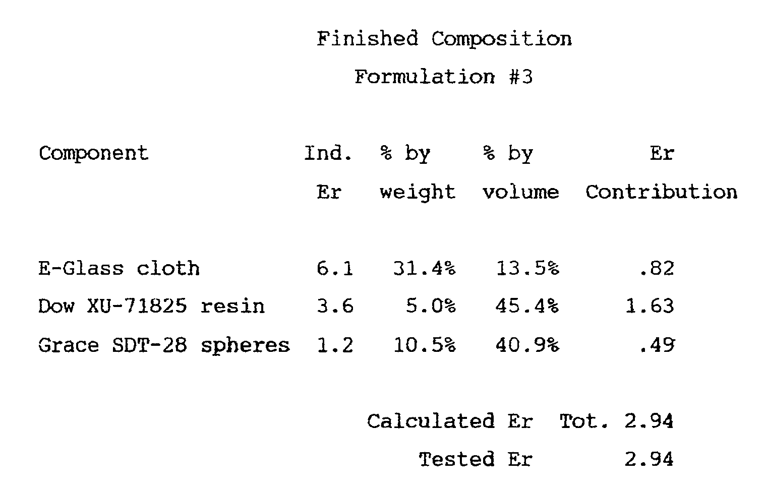
- Specific Formulation #3: The following formulation and procedure were used to make a flame retardant laminate with an Er of 2.85. A solution containing 286 grams of Dow XU 71825.02, (70% by weight epoxy resin in MEK), .2 grams of 2 Methyl Imidazole, 80 grams of MEK and 36 grams of Grace Syntactics SDT-28 microspheres was prepared. The microspheres had previously been treated with a 1% solution of Dow/Corning X1-6100 silane coupler. Standard 108 Style E-Glass cloth supplied by UniGlass of New York, New York and treated with UM718 silane coupler was impregnated with this mixture. The impregnation gap setting was 305 µm (.012 inches). The resulting fabric was B-stage cured in an oven for 4 minutes at 138°C. Resin/microsphere pick-up was measured to be 67.8%. Prepreg flow level was tested under standard conditions, 2068 kPa (300PSI), 177°C for 8 minutes and found to be 31.3%. This flow level is considered excessive; the ideal flow level is thought to be around 20% for a microsphere laminate. Three ply laminates with 35,56 µm (.0014 in.) thick copper on both sides and one ten ply laminate for flammability testing were made by press lamination at 177°C at 2068 kPa (300PSI) for 80 minutes. Flammability was tested. Average extinguishing times for the first and second burns were 2.5 and .2 seconds respectively, giving an equivalent UL94-V0 rating. Tan Phi was found to be .149. This Tan Phi number is considered slightly high and would have been reduced if the optimum coupling agent had been applied to the spheres. The dielectric constant was measured using the "Spectrum analyzer technique" at 292 MHz and 590 MHz, and the Er's were found to be 2.90 and 2.85 respectively. Prepreg pressed thickness was found to be 114,3 µm (.0045 inches) per ply. The following table gives a detailed analysis of the composition and the resulting Er of this laminate.
- Specific Formulation #4: The following formulation and procedure were used to make a flame retardant laminate with an Er of 2.23. A solution containing 286 grams of Arocy F-40, (75% by weight epoxy resin in MEK), .3 grams of Zinc Octonate, (8% Zn), 70 grams of MEK and 79 grams of 3M experimental small microspheres was prepared. The microspheres had not been treated with a silane coupling agent. Woven PTFE fabric was impregnated with this mixture. The impregnation gap setting was 178 µm (.007 inches). The resulting fabric was B-stage cured in an oven for 4 minutes at 138°C. Resin/microsphere pick-up was measured to be 56.8%. Prepreg flow level was not tested. One three ply laminate with 35,56 µm (.0014 inch) thick copper on both sides and one ten ply laminate for flammability testing were made by press lamination at 320°C and 2068 kPa (300PSI) for 60 minutes. Flammability was tested. Average extinguishing times for the first and second burns were 1.0 and 0 seconds respectively, (0 means that it did not burn) giving an equivalent UL94-V0 rating. Er was measured using the "Spectrum analyzer technique" at 390 MHz and 796 MHz, and the Er's were found to be 2.27 and 2.19 respectively. The following table gives a detailed analysis of the composition and the resulting Er of the laminate.

- Specific Formulation #5: The following formulation and procedure were used to make a flame retardant laminate with an Er of 2.75. A solution containing 286 grams of Ciba-Geigy Araldite* 87-212, (70% by weight epoxy resin in MEK), .4 grams of 2 Methyl Imidazole, 70 grams of MEK and 36 grams of Grace Syntactics SDT-28 microspheres was prepared. The microspheres had previously been treated with a 1% solution of 90/10% by weight mixture of Dow/Corning Z-6075 and Z-6020 coupling agent respectively. Standard 108 style E-Glass cloth supplied by UniGlass and treated with UM718 silane coupler was impregnated with this mixture. The impregnation gap setting was 305 µm (.012 inches). The resulting fabric was B-stage cured in an oven for 3 minutes at 143°C. Resin/microsphere pick-up was measured to be 68.8%. Prepreg flow level was tested under standard conditions, 2068 kPa (300 PSI), 177°C for 8 minutes and found to be 10.6%. Three ply laminates with 35,56 µm (.0014 in.) thick copper on both sides and one ten ply laminate for flammability testing were made by press lamination at 177°C at 2758 kPa (400 PSI) for 90 minutes. Flammability was tested. Average extinguishing times for the first and second burns were 2.0 and 0 seconds respectively, giving an equivalent UL94-V0 rating. Tan Phi was tested and was found to be .092. Er was tested using the "Spectrum analyzer technique" at 312 MHz and 631 MHz, the Er's were found to be 2.83 and 2.77 respectively. Prepreg pressed thickness was found to be 114,3 µm (.0045 inches) per ply. The following table gives a detailed analysis of the composition and the resulting Er of this laminate.
- The formulations of both the liquid impregnation mix and the finished laminate are also shown below. It can be seen that although the microspheres account for only a small percentage of the total weight of the final composite material, they make up almost half of the total volume. This is due to the extremely low density of the microspheres, (.28 g/cc), for the Grace Syntactics SDT-28 microspheres.

- The above table gives amounts used for one specific formulation. The individual ingredient percentages can be varied depending on the exact properties desired for the final composite. In general the composition is a laminate comprised of 7-30 vol% reinforcing fabric and 70-93 vol% of a microsphere filled resin. The microsphere filled resin is comprised of Araldite* 87-212, 80-95 parts by weight and Grace Syntactics SDT-28 microspheres, 5-20% parts by weight and 2-Methyl Imidazole catalyst in the range of .1 parts per hundred of resin. Of course alternative resins, fabrics and fillers may be used. Use of lower weight fabrics of the same carrier material yields thinner prepreg pressed thicknesses. In addition UV blocking dyes are sometimes added to facilitate photolithography operations on very thin laminate cores. These UV absorbing materials can be added in the range .5 parts per hundred (PHR) of resin.
- Below is a table which lists the fundamental properties obtained during extensive testing of the flame retardant microsphere laminate of the present invention identified as Formulation #5. Test methods used are from the IPC test methods manual, (IPC-TMM-650), unless otherwise specified.

- When the formulation and processing as described above are employed, a fire retardant, high quality, cost competitive, reliable, low Er microsphere laminate circuit board can be manufactured which exhibits low shrink warpage on processing, low dielectric constant, low wet dissipation tangent, acceptable dielectric breakdown voltage, acceptable adhesive strength, low CTE and low moisture absorption, and which passes solder shock testing and possesses a high Tg.
Claims (13)
- A filled prepreg material having a dielectric constant below 3.2, comprising:
at least one polymer resin;
hollow inorganic microsphere filler;
a coupling agent; and
reinforcement material. - The prepreg material recited in claim 1 wherein the polymer resin is selected from the group consisting of cyanate, epoxy, benzocyclobutane, polyimide, fluoropolymer and fluorinated dicyanate.
- The prepreg material recited in claim 1 or 2, wherein the hollow inorganic microspheres of the filler are randomly distributed and exhibit a compressive strength of between about 3,447 to about 34,47 MPa (about 500 to about 5000 pounds per square inch).
- The prepreg material recited in claim 1, 2 or 3, wherein the reinforcement material comprises a woven cloth, mat or film selected from the group consisting of glass, ceramic, fluoropolymer, polyester, quartz, polyimide, Kevlar, Nomex, poly p-phenylene benzobisthiazole, poly p-phenylene benzobisoxazole, Aramid, polyetheretherketone, and aromatic polyester.
- The prepreg material recited in any one of the preceding claims, wherein the polymer resin and hollow inorganic microsphere filler comprise a flame retardant material.
- The prepreg material recited in any one of the preceding claims, comprising in addition a UV blocking dye for rendering the laminate opaque to UV wavelength light.
- The prepreg material recited in any one of the preceding claims, wherein the hollow inorganic microspheres of the filler have a maximum diameter of less than about 40 microns.
- The prepreg material recited in any one of the preceding claims, wherein about 90% of the hollow inorganic microspheres of the filler are glass or silica walled and have a mean diameter between about 5 microns to about 25 microns and comprise about 2% by weight or less of sodium oxide.
- The prepreg material recited in claim 8, wherein the hollow glass microspheres of the filler comprise from about 25 to about 65 percent by volume.
- A printed circuit board comprising a prepreg material having a dielectric constant below 3.2, which material includes at least one polymer resin; hollow inorganic microsphere filler; a silane coupling agent; and reinforcement material, the circuit board also including at least one layer of conductive material disposed on at least a portion thereof.
- A method of making a printed circuit board including prepreg material having a dielectric constant less than 3.2, comprising:a) coating hollow inorganic microsphere filler with a silane coupling agent;b) making a randomly distributed mixture of polymer resin, solvent and the silane coated microspheres;c) impregnating a reinforcement material with the randomly distributed mixture to form a prepreg material;d) partially curing the impregnated reinforcement material;e) cladding the partially cured impregnated reinforcement material with at least one layer of metal; andf) laminating together a plurality of laminates metal clad impregnated reinforcement material under heat and pressure.
- The method recited in claim 11, including in addition the step of drilling at least one through hole.
- The method recited in claim 11, wherein the step of coating of hollow inorganic microsphere filler with a coupling agent comprises coating of hollow inorganic microsphere filler having a mean diameter of about 5 microns to about 15 microns.
Applications Claiming Priority (2)
| Application Number | Priority Date | Filing Date | Title |
|---|---|---|---|
| US470453 | 1990-01-26 | ||
| US07/470,453 US5126192A (en) | 1990-01-26 | 1990-01-26 | Flame retardant, low dielectric constant microsphere filled laminate |
Publications (2)
| Publication Number | Publication Date |
|---|---|
| EP0440918A2 true EP0440918A2 (en) | 1991-08-14 |
| EP0440918A3 EP0440918A3 (en) | 1992-02-26 |
Family
ID=23867692
Family Applications (1)
| Application Number | Title | Priority Date | Filing Date |
|---|---|---|---|
| EP19900123488 Withdrawn EP0440918A3 (en) | 1990-01-26 | 1990-12-07 | Flame retardant, low dielectric constant microsphere filled laminate |
Country Status (3)
| Country | Link |
|---|---|
| US (1) | US5126192A (en) |
| EP (1) | EP0440918A3 (en) |
| JP (1) | JP2589874B2 (en) |
Cited By (11)
| Publication number | Priority date | Publication date | Assignee | Title |
|---|---|---|---|---|
| DE4209381A1 (en) * | 1991-03-29 | 1992-10-01 | Matsushita Electric Works Ltd | POLYIMIDE COMPOSITION AND PREPREG AND LAMINATE MADE THEREOF |
| EP0512401A2 (en) * | 1991-05-03 | 1992-11-11 | International Business Machines Corporation | Low dielectric constant composite laminates filled with molecularly porous aerogels |
| DE4135678A1 (en) * | 1991-10-30 | 1993-05-06 | Chemie Linz (Deutschland) Gmbh, 6200 Wiesbaden, De | Thermally expandable fire protection materials - contain expanded graphite, polymeric binders, substances which form carbon skeleton when exposed to fire, and hollow microspheres, etc. |
| EP0581314A2 (en) * | 1992-07-31 | 1994-02-02 | International Business Machines Corporation | Modified dicyanate ester resins having enhanced fracture thoughness |
| US5785789A (en) * | 1993-03-18 | 1998-07-28 | Digital Equipment Corporation | Low dielectric constant microsphere filled layers for multilayer electrical structures |
| US6277203B1 (en) | 1998-09-29 | 2001-08-21 | Lam Research Corporation | Method and apparatus for cleaning low K dielectric and metal wafer surfaces |
| WO2010009381A1 (en) * | 2008-07-18 | 2010-01-21 | World Properties, Inc. | Circuit materials, circuits laminates, and method of manufacture thereof |
| CN102625574A (en) * | 2012-03-31 | 2012-08-01 | 浙江华正新材料股份有限公司 | Low-dielectric-constant PCB (Printed Circuit Board) base plate and manufacturing method thereof |
| WO2013044618A1 (en) * | 2011-09-29 | 2013-04-04 | 深圳光启高等理工研究院 | Microstrip |
| CN103035993A (en) * | 2011-09-29 | 2013-04-10 | 深圳光启高等理工研究院 | Microstrip line |
| WO2018183787A1 (en) * | 2017-03-31 | 2018-10-04 | Magna Seating Inc. | Electrical circuit board with low thermal conductivity and method of constructing thereof |
Families Citing this family (80)
| Publication number | Priority date | Publication date | Assignee | Title |
|---|---|---|---|---|
| US5312576B1 (en) * | 1991-05-24 | 2000-04-18 | World Properties Inc | Method for making particulate filled composite film |
| US5312691A (en) * | 1991-09-10 | 1994-05-17 | Glasteel Industrial Laminates, Inc. | Copper-clad MC4 unsaturated polyester resin |
| US5348990A (en) * | 1993-03-02 | 1994-09-20 | Hoechst Celanese Corp. | Low dielectric materials |
| US5677045A (en) * | 1993-09-14 | 1997-10-14 | Hitachi, Ltd. | Laminate and multilayer printed circuit board |
| US5552092A (en) * | 1994-05-31 | 1996-09-03 | Corning Incorporated | Waveguide coupler |
| DE4423893C2 (en) * | 1994-07-07 | 1996-09-05 | Freudenberg Carl Fa | Flat gasket with flexible circuit board |
| US5879794A (en) * | 1994-08-25 | 1999-03-09 | W. L. Gore & Associates, Inc. | Adhesive-filler film composite |
| US5753358A (en) * | 1994-08-25 | 1998-05-19 | W. L. Gore & Associates, Inc. | Adhisive-filler polymer film composite |
| US5766750A (en) * | 1994-08-25 | 1998-06-16 | W. L. Gore & Associates, Inc. | Process for making an adhesive-filler polymer film composite |
| DE69519591D1 (en) * | 1995-01-06 | 2001-01-11 | Colibri Panel As Hareid | USE OF A SANDWICH COMPONENT AS FIRE INSULATION OR FIRE SEPARATION AND METHOD FOR THE CONTINUOUS PRODUCTION OF THESE SANDWICH COMPONENTS |
| US5670250A (en) * | 1995-02-24 | 1997-09-23 | Polyclad Laminates, Inc. | Circuit board prepreg with reduced dielectric constant |
| JP3488547B2 (en) * | 1995-03-03 | 2004-01-19 | 日東電工株式会社 | Resonant circuit tag, method of manufacturing the same, and method of changing resonance characteristics thereof |
| US5889104A (en) * | 1996-01-11 | 1999-03-30 | W. L. Gore & Associates, Inc. | Low dielectric constant material for use as an insulation element in an electronic device |
| US5835987A (en) | 1995-10-31 | 1998-11-10 | Micron Technology, Inc. | Reduced RC delay between adjacent substrate wiring lines |
| US5691059A (en) * | 1995-11-21 | 1997-11-25 | Minnesota Mining And Manfacturing Company | Glass and glass-ceramic bubbles having an aluminum nitride coating |
| AU4902897A (en) * | 1996-11-08 | 1998-05-29 | W.L. Gore & Associates, Inc. | Method for improving reliability of thin circuit substrates by increasing the T of the substrate |
| KR20010005944A (en) * | 1997-04-03 | 2001-01-15 | 캠벨 존 에스 | Low dielectric constant material with improved dielectric strength |
| US6042936A (en) * | 1997-09-23 | 2000-03-28 | Fibermark, Inc. | Microsphere containing circuit board paper |
| US6440641B1 (en) | 1998-07-31 | 2002-08-27 | Kulicke & Soffa Holdings, Inc. | Deposited thin film build-up layer dimensions as a method of relieving stress in high density interconnect printed wiring board substrates |
| JP4348785B2 (en) * | 1999-07-29 | 2009-10-21 | 三菱瓦斯化学株式会社 | High elastic modulus glass cloth base thermosetting resin copper clad laminate |
| US6596624B1 (en) | 1999-07-31 | 2003-07-22 | International Business Machines Corporation | Process for making low dielectric constant hollow chip structures by removing sacrificial dielectric material after the chip is joined to a chip carrier |
| JP4180825B2 (en) * | 2000-01-26 | 2008-11-12 | インターナショナル・ペーパー・カンパニー | Low density paperboard articles |
| US6866906B2 (en) | 2000-01-26 | 2005-03-15 | International Paper Company | Cut resistant paper and paper articles and method for making same |
| JP2003003134A (en) * | 2001-06-20 | 2003-01-08 | Japan Gore Tex Inc | Sheet for ic chip adhesion and ic package |
| US6632511B2 (en) | 2001-11-09 | 2003-10-14 | Polyclad Laminates, Inc. | Manufacture of prepregs and laminates with relatively low dielectric constant for printed circuit boards |
| AU2003272481A1 (en) | 2002-09-13 | 2004-04-30 | Yang, Sen | Paper with improved stiffness and bulk and method for making same |
| AU2002953099A0 (en) * | 2002-12-04 | 2002-12-19 | Australian Composites Pty Ltd | Reinforced polymer composition |
| US20040224590A1 (en) * | 2003-03-31 | 2004-11-11 | George Rawa | Thermoplastic/fiber material composites, composite/metallic articles and methods for making composite/metallic articles |
| US7164197B2 (en) * | 2003-06-19 | 2007-01-16 | 3M Innovative Properties Company | Dielectric composite material |
| US7033670B2 (en) * | 2003-07-11 | 2006-04-25 | Siemens Power Generation, Inc. | LCT-epoxy polymers with HTC-oligomers and method for making the same |
| US7781063B2 (en) | 2003-07-11 | 2010-08-24 | Siemens Energy, Inc. | High thermal conductivity materials with grafted surface functional groups |
| JP4325337B2 (en) | 2003-09-19 | 2009-09-02 | 日立化成工業株式会社 | Resin composition, prepreg, laminate and multilayer printed wiring board using the same |
| US20100280164A1 (en) | 2009-04-29 | 2010-11-04 | Tundra Composites, LLC. | Inorganic Composite |
| US9105382B2 (en) | 2003-11-14 | 2015-08-11 | Tundra Composites, LLC | Magnetic composite |
| US7931830B2 (en) * | 2004-03-31 | 2011-04-26 | Endicott Interconnect Technologies, Inc. | Dielectric composition for use in circuitized substrates and circuitized substrate including same |
| US7429789B2 (en) * | 2004-03-31 | 2008-09-30 | Endicott Interconnect Technologies, Inc. | Fluoropolymer dielectric composition for use in circuitized substrates and circuitized substrate including same |
| US7553781B2 (en) * | 2004-06-15 | 2009-06-30 | Siemens Energy, Inc. | Fabrics with high thermal conductivity coatings |
| US8216672B2 (en) * | 2004-06-15 | 2012-07-10 | Siemens Energy, Inc. | Structured resin systems with high thermal conductivity fillers |
| US7776392B2 (en) * | 2005-04-15 | 2010-08-17 | Siemens Energy, Inc. | Composite insulation tape with loaded HTC materials |
| US20050274774A1 (en) * | 2004-06-15 | 2005-12-15 | Smith James D | Insulation paper with high thermal conductivity materials |
| US7553438B2 (en) * | 2004-06-15 | 2009-06-30 | Siemens Energy, Inc. | Compression of resin impregnated insulating tapes |
| US7592045B2 (en) * | 2004-06-15 | 2009-09-22 | Siemens Energy, Inc. | Seeding of HTC fillers to form dendritic structures |
| US20080050580A1 (en) * | 2004-06-15 | 2008-02-28 | Stevens Gary C | High Thermal Conductivity Mica Paper Tape |
| US20050277721A1 (en) | 2004-06-15 | 2005-12-15 | Siemens Westinghouse Power Corporation | High thermal conductivity materials aligned within resins |
| KR20060045208A (en) * | 2004-11-12 | 2006-05-17 | 삼성테크윈 주식회사 | Printed circuit for semi-conductor package and method for manufacturing the same |
| JP5302670B2 (en) | 2005-03-11 | 2013-10-02 | インターナショナル・ペーパー・カンパニー | Compositions containing expandable microspheres and ionic compounds, and methods for making and using these compositions |
| US7846853B2 (en) * | 2005-04-15 | 2010-12-07 | Siemens Energy, Inc. | Multi-layered platelet structure |
| US7651963B2 (en) * | 2005-04-15 | 2010-01-26 | Siemens Energy, Inc. | Patterning on surface with high thermal conductivity materials |
| US20060275616A1 (en) * | 2005-06-03 | 2006-12-07 | Clough Robert S | Silane-based coupling agent |
| US7851059B2 (en) * | 2005-06-14 | 2010-12-14 | Siemens Energy, Inc. | Nano and meso shell-core control of physical properties and performance of electrically insulating composites |
| US20070026221A1 (en) * | 2005-06-14 | 2007-02-01 | Siemens Power Generation, Inc. | Morphological forms of fillers for electrical insulation |
| US7655295B2 (en) | 2005-06-14 | 2010-02-02 | Siemens Energy, Inc. | Mix of grafted and non-grafted particles in a resin |
| US7781057B2 (en) * | 2005-06-14 | 2010-08-24 | Siemens Energy, Inc. | Seeding resins for enhancing the crystallinity of polymeric substructures |
| US8357433B2 (en) * | 2005-06-14 | 2013-01-22 | Siemens Energy, Inc. | Polymer brushes |
| US7955661B2 (en) * | 2005-06-14 | 2011-06-07 | Siemens Energy, Inc. | Treatment of micropores in mica materials |
| US20070004844A1 (en) * | 2005-06-30 | 2007-01-04 | Clough Robert S | Dielectric material |
| US20070090545A1 (en) * | 2005-10-24 | 2007-04-26 | Condie Brian W | Semiconductor device with improved encapsulation |
| JP5309316B2 (en) * | 2006-02-06 | 2013-10-09 | 国立大学法人東北大学 | Chip element |
| US7658988B2 (en) * | 2006-04-03 | 2010-02-09 | E. I. Du Pont De Nemours And Company | Printed circuits prepared from filled epoxy compositions |
| US7547847B2 (en) * | 2006-09-19 | 2009-06-16 | Siemens Energy, Inc. | High thermal conductivity dielectric tape |
| US8445101B2 (en) | 2007-03-21 | 2013-05-21 | Ashtech Industries, Llc | Sound attenuation building material and system |
| CA2681528C (en) | 2007-03-21 | 2018-10-23 | Ashtech Industries, Llc | Utility materials incorporating a microparticle matrix |
| US20090239429A1 (en) | 2007-03-21 | 2009-09-24 | Kipp Michael D | Sound Attenuation Building Material And System |
| MX2010007764A (en) | 2008-01-18 | 2010-11-10 | Wild River Consulting Group Llc | Melt molding polymer composite and method of making and using the same. |
| US8382945B2 (en) | 2008-08-28 | 2013-02-26 | International Paper Company | Expandable microspheres and methods of making and using the same |
| US8591677B2 (en) | 2008-11-04 | 2013-11-26 | Ashtech Industries, Llc | Utility materials incorporating a microparticle matrix formed with a setting agent |
| US20110017498A1 (en) * | 2009-07-27 | 2011-01-27 | Endicott Interconnect Technologies, Inc. | Photosensitive dielectric film |
| US20110207866A1 (en) * | 2010-02-25 | 2011-08-25 | Japp Robert M | Halogen-Free Dielectric Composition For use As Dielectric Layer In Circuitized Substrates |
| US8309210B1 (en) * | 2010-09-13 | 2012-11-13 | Rockell Collins, Inc. | Printed wiring board pad cratering inhibitor |
| CN103180138B (en) * | 2010-10-25 | 2016-03-16 | 大金工业株式会社 | Metal-clad laminate and manufacture method thereof and flexible printed board |
| US8693203B2 (en) | 2011-01-14 | 2014-04-08 | Harris Corporation | Method of making an electronic device having a liquid crystal polymer solder mask laminated to an interconnect layer stack and related devices |
| US8912807B2 (en) * | 2011-09-09 | 2014-12-16 | General Electric Company | Sensor devices and methods for use in sensing current through a conductor |
| US9497849B2 (en) * | 2012-07-10 | 2016-11-15 | Ibiden Co., Ltd. | Printed wiring board |
| WO2014171957A1 (en) * | 2013-04-18 | 2014-10-23 | Brook One Corporation | Burnthrough resistant laminate film |
| EP3025566B1 (en) | 2013-07-23 | 2021-04-07 | Rogers Corporation | Circuit materials, circuit laminates, and methods of manufacture thereof |
| US9818682B2 (en) * | 2014-12-03 | 2017-11-14 | International Business Machines Corporation | Laminate substrates having radial cut metallic planes |
| JP6882466B2 (en) | 2016-10-24 | 2021-06-02 | サン−ゴバン パフォーマンス プラスティックス コーポレイション | Polymer composition, materials and manufacturing methods |
| WO2021060764A1 (en) * | 2019-09-23 | 2021-04-01 | 주식회사 아모그린텍 | Rf heat dissipation plastic and repeater cabinet implemented by including same |
| CN116144220B (en) * | 2023-02-07 | 2024-01-02 | 北京石油化工学院 | Low-density solid flame-retardant buoyancy material and preparation method and application thereof |
| CN116333587B (en) * | 2023-05-31 | 2023-09-01 | 北京爱思达航天科技有限公司 | Low-dielectric-constant hydrophobic moisture-proof coating for wave-transparent material and application thereof |
Citations (4)
| Publication number | Priority date | Publication date | Assignee | Title |
|---|---|---|---|---|
| US3523037A (en) * | 1967-06-12 | 1970-08-04 | Ibm | Epoxy resin composition containing brominated polyglycidyl ether of bisphenol a and a polyglycidyl ether of tetrakis(hydroxyphenyl) ethane |
| SU1065443A1 (en) * | 1982-08-30 | 1984-01-07 | Предприятие П/Я А-1944 | Multiple-layer prepreg |
| EP0211979A1 (en) * | 1985-08-14 | 1987-03-04 | Toray Industries, Inc. | Laminate board containing uniformly distributed filler particles and method for producing the same |
| EP0304699A2 (en) * | 1987-08-28 | 1989-03-01 | Junkosha Co. Ltd. | Composite material of low dielectric constant and method of producing it |
Family Cites Families (21)
| Publication number | Priority date | Publication date | Assignee | Title |
|---|---|---|---|---|
| US3700538A (en) * | 1970-09-10 | 1972-10-24 | Nasa | Polyimide resin-fiberglass cloth laminates for printed circuit boards |
| US4309334A (en) * | 1975-10-08 | 1982-01-05 | Loctite Corporation | Thermally-resistant glass-filled adhesive/sealant compositions |
| US4134848A (en) * | 1976-06-28 | 1979-01-16 | The United States Of America As Represented By The Secretary Of The Navy | Composite for improved stripline board material |
| JPS5511351A (en) * | 1978-07-12 | 1980-01-26 | Nippon Telegraph & Telephone | Substrate for printed circuit board |
| US4241132A (en) * | 1978-08-17 | 1980-12-23 | Castall Incorporated | Insulating boards |
| US4268337A (en) * | 1978-08-24 | 1981-05-19 | Asahi Kasei Kogyo Kabushiki Kaisha | Sheet molding material produced by associating a layer comprising a photopolymerizable material with layers comprising thermosetting resins |
| US4335180A (en) * | 1978-12-26 | 1982-06-15 | Rogers Corporation | Microwave circuit boards |
| DE3068776D1 (en) * | 1979-04-20 | 1984-09-06 | Secr Defence Brit | Resin materials, their use and article thereof |
| US4238641A (en) * | 1979-09-26 | 1980-12-09 | Bunker Ramo Corporation | Composite epoxy glass-microsphere-dielectrics for electronic coaxial structures |
| US4447565A (en) * | 1981-12-07 | 1984-05-08 | The United States Of America As Represented By The United States Department Of Energy | Method and composition for molding low density desiccant syntactic foam articles |
| JPS60167394A (en) * | 1984-02-09 | 1985-08-30 | 東レ株式会社 | Circuit board |
| JPS60214941A (en) * | 1984-04-10 | 1985-10-28 | 株式会社 潤工社 | Printed substrate |
| US4680220A (en) * | 1985-02-26 | 1987-07-14 | W. L. Gore & Associates, Inc. | Dielectric materials |
| US4610495A (en) * | 1985-03-07 | 1986-09-09 | Rogers Corporation | Solderless connector apparatus and method of making the same |
| US4657809A (en) * | 1985-09-18 | 1987-04-14 | Eskind Larry G | Fire retardant compositions and use thereof |
| US4788230A (en) * | 1985-09-30 | 1988-11-29 | The Boeing Company | Process for making a low density syntactic foam product and the resultant product |
| JPS62262498A (en) * | 1986-05-08 | 1987-11-14 | 日本電気株式会社 | Multilayer circuit board |
| DE3785487T2 (en) * | 1986-06-02 | 1993-07-29 | Japan Gore Tex Inc | METHOD FOR PRODUCING CARRIERS FOR PRINTED CIRCUITS. |
| US4849284A (en) * | 1987-02-17 | 1989-07-18 | Rogers Corporation | Electrical substrate material |
| GB8709734D0 (en) * | 1987-04-24 | 1987-05-28 | Reckitt & Colmann Prod Ltd | Thiadiazole derivatives |
| JPH02140256A (en) * | 1988-11-18 | 1990-05-29 | Junkosha Co Ltd | Composite material having low dielectric constant |
-
1990
- 1990-01-26 US US07/470,453 patent/US5126192A/en not_active Expired - Fee Related
- 1990-11-30 JP JP2330957A patent/JP2589874B2/en not_active Expired - Fee Related
- 1990-12-07 EP EP19900123488 patent/EP0440918A3/en not_active Withdrawn
Patent Citations (4)
| Publication number | Priority date | Publication date | Assignee | Title |
|---|---|---|---|---|
| US3523037A (en) * | 1967-06-12 | 1970-08-04 | Ibm | Epoxy resin composition containing brominated polyglycidyl ether of bisphenol a and a polyglycidyl ether of tetrakis(hydroxyphenyl) ethane |
| SU1065443A1 (en) * | 1982-08-30 | 1984-01-07 | Предприятие П/Я А-1944 | Multiple-layer prepreg |
| EP0211979A1 (en) * | 1985-08-14 | 1987-03-04 | Toray Industries, Inc. | Laminate board containing uniformly distributed filler particles and method for producing the same |
| EP0304699A2 (en) * | 1987-08-28 | 1989-03-01 | Junkosha Co. Ltd. | Composite material of low dielectric constant and method of producing it |
Non-Patent Citations (1)
| Title |
|---|
| DATABASE WPIL, accession no. 84-218308, Derwent Publications Ltd, London, GB; & SU-A-1 065 443 (L.G. SHIROKOVA) 07-01-1984 * |
Cited By (22)
| Publication number | Priority date | Publication date | Assignee | Title |
|---|---|---|---|---|
| DE4209381A1 (en) * | 1991-03-29 | 1992-10-01 | Matsushita Electric Works Ltd | POLYIMIDE COMPOSITION AND PREPREG AND LAMINATE MADE THEREOF |
| EP0512401A2 (en) * | 1991-05-03 | 1992-11-11 | International Business Machines Corporation | Low dielectric constant composite laminates filled with molecularly porous aerogels |
| EP0512401A3 (en) * | 1991-05-03 | 1993-08-11 | International Business Machines Corporation | Low dielectric constant composite laminates filled with molecularly porous aerogels |
| DE4135678A1 (en) * | 1991-10-30 | 1993-05-06 | Chemie Linz (Deutschland) Gmbh, 6200 Wiesbaden, De | Thermally expandable fire protection materials - contain expanded graphite, polymeric binders, substances which form carbon skeleton when exposed to fire, and hollow microspheres, etc. |
| EP0581314A2 (en) * | 1992-07-31 | 1994-02-02 | International Business Machines Corporation | Modified dicyanate ester resins having enhanced fracture thoughness |
| EP0581314A3 (en) * | 1992-07-31 | 1994-09-07 | Ibm | Modified dicyanate ester resins having enhanced fracture thoughness |
| US5548034A (en) * | 1992-07-31 | 1996-08-20 | International Business Machines Corporation | Modified dicyanate ester resins having enhanced fracture toughness |
| US5785789A (en) * | 1993-03-18 | 1998-07-28 | Digital Equipment Corporation | Low dielectric constant microsphere filled layers for multilayer electrical structures |
| US6277203B1 (en) | 1998-09-29 | 2001-08-21 | Lam Research Corporation | Method and apparatus for cleaning low K dielectric and metal wafer surfaces |
| US6319330B1 (en) | 1998-09-29 | 2001-11-20 | Lam Research Corporation | Method and apparatus for cleaning low K dielectric and metal wafer surfaces |
| WO2010009381A1 (en) * | 2008-07-18 | 2010-01-21 | World Properties, Inc. | Circuit materials, circuits laminates, and method of manufacture thereof |
| GB2473982A (en) * | 2008-07-18 | 2011-03-30 | World Properties Inc | Circuit materials, circuits laminates and method of manufacture thereof |
| US8187696B2 (en) | 2008-07-18 | 2012-05-29 | World Properties, Inc. | Circuit materials, circuits laminates, and method of manufacture thereof |
| GB2473982B (en) * | 2008-07-18 | 2013-01-23 | World Properties Inc | Circuit materials, circuits laminates and method of manufacture thereof |
| WO2013044618A1 (en) * | 2011-09-29 | 2013-04-04 | 深圳光启高等理工研究院 | Microstrip |
| CN103035993A (en) * | 2011-09-29 | 2013-04-10 | 深圳光启高等理工研究院 | Microstrip line |
| CN103035993B (en) * | 2011-09-29 | 2016-05-04 | 深圳光启尖端技术有限责任公司 | microstrip line |
| CN102625574A (en) * | 2012-03-31 | 2012-08-01 | 浙江华正新材料股份有限公司 | Low-dielectric-constant PCB (Printed Circuit Board) base plate and manufacturing method thereof |
| CN102625574B (en) * | 2012-03-31 | 2014-08-06 | 浙江华正新材料股份有限公司 | Low-dielectric-constant PCB (Printed Circuit Board) base plate and manufacturing method thereof |
| WO2018183787A1 (en) * | 2017-03-31 | 2018-10-04 | Magna Seating Inc. | Electrical circuit board with low thermal conductivity and method of constructing thereof |
| CN110476487A (en) * | 2017-03-31 | 2019-11-19 | 麦格纳座椅公司 | Circuit board and its building method with lower thermal conductivity |
| US11259398B2 (en) | 2017-03-31 | 2022-02-22 | Magna Seating Inc. | Electrical circuit board with low thermal conductivity and method of constructing thereof |
Also Published As
| Publication number | Publication date |
|---|---|
| US5126192A (en) | 1992-06-30 |
| JPH03222733A (en) | 1991-10-01 |
| JP2589874B2 (en) | 1997-03-12 |
| EP0440918A3 (en) | 1992-02-26 |
Similar Documents
| Publication | Publication Date | Title |
|---|---|---|
| US5126192A (en) | Flame retardant, low dielectric constant microsphere filled laminate | |
| EP0512401A2 (en) | Low dielectric constant composite laminates filled with molecularly porous aerogels | |
| US7429789B2 (en) | Fluoropolymer dielectric composition for use in circuitized substrates and circuitized substrate including same | |
| US5670250A (en) | Circuit board prepreg with reduced dielectric constant | |
| US7416972B2 (en) | Method of making same low moisture absorptive circuitized substrave with reduced thermal expansion | |
| US7508076B2 (en) | Information handling system including a circuitized substrate having a dielectric layer without continuous fibers | |
| US8445094B2 (en) | Circuitized substrate with dielectric layer having dielectric composition not including continuous or semi-continuous fibers | |
| US8211790B2 (en) | Multilayered circuitized substrate with P-aramid dielectric layers and method of making same | |
| US8198551B2 (en) | Power core for use in circuitized substrate and method of making same | |
| US8084863B2 (en) | Circuitized substrate with continuous thermoplastic support film dielectric layers | |
| JP2007266606A (en) | Fluoropolymer insulating composition for circuit board, and circuit board including same | |
| US7931830B2 (en) | Dielectric composition for use in circuitized substrates and circuitized substrate including same | |
| US7145221B2 (en) | Low moisture absorptive circuitized substrate, method of making same, electrical assembly utilizing same, and information handling system utilizing same | |
| JP2007129215A (en) | Dielectric composition for use in circuit board and circuit board formed using the same | |
| US20090258161A1 (en) | Circuitized substrate with P-aramid dielectric layers and method of making same | |
| US20110207866A1 (en) | Halogen-Free Dielectric Composition For use As Dielectric Layer In Circuitized Substrates | |
| JPH10321974A (en) | Board for forming circuit | |
| JP2003073543A (en) | Resin composition, prepreg and printed circuit board using the same | |
| US5281466A (en) | Low volume fraction ceramic filled fluoropolymeric composite material | |
| Japp et al. | Low dielectric constant laminates containing microspheres | |
| Kelley et al. | Reengineered FR-4 Base Materials for Improved Multilayer PCB Performance | |
| AZUMA | ADHESIVELESS POLYIMIIM: LAMINATE AS A CIIUT1TRY MATEK".. V. | |
| JPH05198904A (en) | Fluoropolymer filled with ceramic in low content | |
| JP2000165000A (en) | Printed wiring board |
Legal Events
| Date | Code | Title | Description |
|---|---|---|---|
| PUAI | Public reference made under article 153(3) epc to a published international application that has entered the european phase |
Free format text: ORIGINAL CODE: 0009012 |
|
| AK | Designated contracting states |
Kind code of ref document: A2 Designated state(s): AT DE ES FR GB |
|
| PUAL | Search report despatched |
Free format text: ORIGINAL CODE: 0009013 |
|
| 17P | Request for examination filed |
Effective date: 19911112 |
|
| AK | Designated contracting states |
Kind code of ref document: A3 Designated state(s): AT DE ES FR GB |
|
| 17Q | First examination report despatched |
Effective date: 19940418 |
|
| STAA | Information on the status of an ep patent application or granted ep patent |
Free format text: STATUS: THE APPLICATION IS DEEMED TO BE WITHDRAWN |
|
| 18D | Application deemed to be withdrawn |
Effective date: 19950715 |