EP0439137A2 - Substrate for packaging a semiconductor device, packaging structure and method - Google Patents
Substrate for packaging a semiconductor device, packaging structure and method Download PDFInfo
- Publication number
- EP0439137A2 EP0439137A2 EP91100821A EP91100821A EP0439137A2 EP 0439137 A2 EP0439137 A2 EP 0439137A2 EP 91100821 A EP91100821 A EP 91100821A EP 91100821 A EP91100821 A EP 91100821A EP 0439137 A2 EP0439137 A2 EP 0439137A2
- Authority
- EP
- European Patent Office
- Prior art keywords
- bump
- packaging
- semiconductor device
- substrate
- recess
- Prior art date
- Legal status (The legal status is an assumption and is not a legal conclusion. Google has not performed a legal analysis and makes no representation as to the accuracy of the status listed.)
- Withdrawn
Links
- 239000000758 substrate Substances 0.000 title claims abstract description 95
- 239000004065 semiconductor Substances 0.000 title claims abstract description 77
- 238000004806 packaging method and process Methods 0.000 title claims abstract description 72
- 238000000034 method Methods 0.000 title claims description 10
- 238000002844 melting Methods 0.000 claims abstract description 36
- 230000008018 melting Effects 0.000 claims abstract description 36
- 239000002184 metal Substances 0.000 claims abstract description 30
- 229910052751 metal Inorganic materials 0.000 claims abstract description 30
- 239000000112 cooling gas Substances 0.000 claims description 8
- 239000000463 material Substances 0.000 claims description 6
- 239000002826 coolant Substances 0.000 claims description 5
- 238000010438 heat treatment Methods 0.000 claims description 5
- 238000007664 blowing Methods 0.000 claims description 2
- 239000004020 conductor Substances 0.000 claims 3
- 238000007747 plating Methods 0.000 claims 1
- 239000007789 gas Substances 0.000 description 4
- 238000012986 modification Methods 0.000 description 2
- 230000004048 modification Effects 0.000 description 2
- 229910052718 tin Inorganic materials 0.000 description 2
- 239000000956 alloy Substances 0.000 description 1
- 229910045601 alloy Inorganic materials 0.000 description 1
- 238000001816 cooling Methods 0.000 description 1
- 239000007772 electrode material Substances 0.000 description 1
- 229910052738 indium Inorganic materials 0.000 description 1
- 239000011261 inert gas Substances 0.000 description 1
- 230000010354 integration Effects 0.000 description 1
- 230000003993 interaction Effects 0.000 description 1
- 229910052745 lead Inorganic materials 0.000 description 1
- 238000001771 vacuum deposition Methods 0.000 description 1
Images


Classifications
-
- H—ELECTRICITY
- H01—ELECTRIC ELEMENTS
- H01L—SEMICONDUCTOR DEVICES NOT COVERED BY CLASS H10
- H01L24/00—Arrangements for connecting or disconnecting semiconductor or solid-state bodies; Methods or apparatus related thereto
- H01L24/80—Methods for connecting semiconductor or other solid state bodies using means for bonding being attached to, or being formed on, the surface to be connected
- H01L24/81—Methods for connecting semiconductor or other solid state bodies using means for bonding being attached to, or being formed on, the surface to be connected using a bump connector
-
- H—ELECTRICITY
- H01—ELECTRIC ELEMENTS
- H01L—SEMICONDUCTOR DEVICES NOT COVERED BY CLASS H10
- H01L23/00—Details of semiconductor or other solid state devices
- H01L23/12—Mountings, e.g. non-detachable insulating substrates
- H01L23/13—Mountings, e.g. non-detachable insulating substrates characterised by the shape
-
- H—ELECTRICITY
- H01—ELECTRIC ELEMENTS
- H01L—SEMICONDUCTOR DEVICES NOT COVERED BY CLASS H10
- H01L23/00—Details of semiconductor or other solid state devices
- H01L23/34—Arrangements for cooling, heating, ventilating or temperature compensation ; Temperature sensing arrangements
- H01L23/46—Arrangements for cooling, heating, ventilating or temperature compensation ; Temperature sensing arrangements involving the transfer of heat by flowing fluids
- H01L23/467—Arrangements for cooling, heating, ventilating or temperature compensation ; Temperature sensing arrangements involving the transfer of heat by flowing fluids by flowing gases, e.g. air
-
- H—ELECTRICITY
- H01—ELECTRIC ELEMENTS
- H01L—SEMICONDUCTOR DEVICES NOT COVERED BY CLASS H10
- H01L2224/00—Indexing scheme for arrangements for connecting or disconnecting semiconductor or solid-state bodies and methods related thereto as covered by H01L24/00
- H01L2224/01—Means for bonding being attached to, or being formed on, the surface to be connected, e.g. chip-to-package, die-attach, "first-level" interconnects; Manufacturing methods related thereto
- H01L2224/10—Bump connectors; Manufacturing methods related thereto
- H01L2224/15—Structure, shape, material or disposition of the bump connectors after the connecting process
- H01L2224/16—Structure, shape, material or disposition of the bump connectors after the connecting process of an individual bump connector
- H01L2224/161—Disposition
- H01L2224/16151—Disposition the bump connector connecting between a semiconductor or solid-state body and an item not being a semiconductor or solid-state body, e.g. chip-to-substrate, chip-to-passive
- H01L2224/16221—Disposition the bump connector connecting between a semiconductor or solid-state body and an item not being a semiconductor or solid-state body, e.g. chip-to-substrate, chip-to-passive the body and the item being stacked
- H01L2224/16225—Disposition the bump connector connecting between a semiconductor or solid-state body and an item not being a semiconductor or solid-state body, e.g. chip-to-substrate, chip-to-passive the body and the item being stacked the item being non-metallic, e.g. insulating substrate with or without metallisation
- H01L2224/16237—Disposition the bump connector connecting between a semiconductor or solid-state body and an item not being a semiconductor or solid-state body, e.g. chip-to-substrate, chip-to-passive the body and the item being stacked the item being non-metallic, e.g. insulating substrate with or without metallisation the bump connector connecting to a bonding area disposed in a recess of the surface of the item
-
- H—ELECTRICITY
- H01—ELECTRIC ELEMENTS
- H01L—SEMICONDUCTOR DEVICES NOT COVERED BY CLASS H10
- H01L2224/00—Indexing scheme for arrangements for connecting or disconnecting semiconductor or solid-state bodies and methods related thereto as covered by H01L24/00
- H01L2224/80—Methods for connecting semiconductor or other solid state bodies using means for bonding being attached to, or being formed on, the surface to be connected
- H01L2224/81—Methods for connecting semiconductor or other solid state bodies using means for bonding being attached to, or being formed on, the surface to be connected using a bump connector
- H01L2224/8112—Aligning
- H01L2224/81136—Aligning involving guiding structures, e.g. spacers or supporting members
- H01L2224/81138—Aligning involving guiding structures, e.g. spacers or supporting members the guiding structures being at least partially left in the finished device
- H01L2224/8114—Guiding structures outside the body
-
- H—ELECTRICITY
- H01—ELECTRIC ELEMENTS
- H01L—SEMICONDUCTOR DEVICES NOT COVERED BY CLASS H10
- H01L2224/00—Indexing scheme for arrangements for connecting or disconnecting semiconductor or solid-state bodies and methods related thereto as covered by H01L24/00
- H01L2224/80—Methods for connecting semiconductor or other solid state bodies using means for bonding being attached to, or being formed on, the surface to be connected
- H01L2224/81—Methods for connecting semiconductor or other solid state bodies using means for bonding being attached to, or being formed on, the surface to be connected using a bump connector
- H01L2224/8119—Arrangement of the bump connectors prior to mounting
- H01L2224/81191—Arrangement of the bump connectors prior to mounting wherein the bump connectors are disposed only on the semiconductor or solid-state body
-
- H—ELECTRICITY
- H01—ELECTRIC ELEMENTS
- H01L—SEMICONDUCTOR DEVICES NOT COVERED BY CLASS H10
- H01L2224/00—Indexing scheme for arrangements for connecting or disconnecting semiconductor or solid-state bodies and methods related thereto as covered by H01L24/00
- H01L2224/80—Methods for connecting semiconductor or other solid state bodies using means for bonding being attached to, or being formed on, the surface to be connected
- H01L2224/81—Methods for connecting semiconductor or other solid state bodies using means for bonding being attached to, or being formed on, the surface to be connected using a bump connector
- H01L2224/818—Bonding techniques
- H01L2224/81801—Soldering or alloying
-
- H—ELECTRICITY
- H01—ELECTRIC ELEMENTS
- H01L—SEMICONDUCTOR DEVICES NOT COVERED BY CLASS H10
- H01L2924/00—Indexing scheme for arrangements or methods for connecting or disconnecting semiconductor or solid-state bodies as covered by H01L24/00
- H01L2924/01—Chemical elements
- H01L2924/01033—Arsenic [As]
-
- H—ELECTRICITY
- H01—ELECTRIC ELEMENTS
- H01L—SEMICONDUCTOR DEVICES NOT COVERED BY CLASS H10
- H01L2924/00—Indexing scheme for arrangements or methods for connecting or disconnecting semiconductor or solid-state bodies as covered by H01L24/00
- H01L2924/01—Chemical elements
- H01L2924/0105—Tin [Sn]
-
- H—ELECTRICITY
- H01—ELECTRIC ELEMENTS
- H01L—SEMICONDUCTOR DEVICES NOT COVERED BY CLASS H10
- H01L2924/00—Indexing scheme for arrangements or methods for connecting or disconnecting semiconductor or solid-state bodies as covered by H01L24/00
- H01L2924/01—Chemical elements
- H01L2924/01061—Promethium [Pm]
-
- H—ELECTRICITY
- H01—ELECTRIC ELEMENTS
- H01L—SEMICONDUCTOR DEVICES NOT COVERED BY CLASS H10
- H01L2924/00—Indexing scheme for arrangements or methods for connecting or disconnecting semiconductor or solid-state bodies as covered by H01L24/00
- H01L2924/01—Chemical elements
- H01L2924/01078—Platinum [Pt]
-
- H—ELECTRICITY
- H01—ELECTRIC ELEMENTS
- H01L—SEMICONDUCTOR DEVICES NOT COVERED BY CLASS H10
- H01L2924/00—Indexing scheme for arrangements or methods for connecting or disconnecting semiconductor or solid-state bodies as covered by H01L24/00
- H01L2924/01—Chemical elements
- H01L2924/01079—Gold [Au]
-
- H—ELECTRICITY
- H01—ELECTRIC ELEMENTS
- H01L—SEMICONDUCTOR DEVICES NOT COVERED BY CLASS H10
- H01L2924/00—Indexing scheme for arrangements or methods for connecting or disconnecting semiconductor or solid-state bodies as covered by H01L24/00
- H01L2924/01—Chemical elements
- H01L2924/01082—Lead [Pb]
-
- H—ELECTRICITY
- H01—ELECTRIC ELEMENTS
- H01L—SEMICONDUCTOR DEVICES NOT COVERED BY CLASS H10
- H01L2924/00—Indexing scheme for arrangements or methods for connecting or disconnecting semiconductor or solid-state bodies as covered by H01L24/00
- H01L2924/01—Chemical elements
- H01L2924/01084—Polonium [Po]
-
- H—ELECTRICITY
- H01—ELECTRIC ELEMENTS
- H01L—SEMICONDUCTOR DEVICES NOT COVERED BY CLASS H10
- H01L2924/00—Indexing scheme for arrangements or methods for connecting or disconnecting semiconductor or solid-state bodies as covered by H01L24/00
- H01L2924/10—Details of semiconductor or other solid state devices to be connected
- H01L2924/11—Device type
- H01L2924/14—Integrated circuits
-
- H—ELECTRICITY
- H05—ELECTRIC TECHNIQUES NOT OTHERWISE PROVIDED FOR
- H05K—PRINTED CIRCUITS; CASINGS OR CONSTRUCTIONAL DETAILS OF ELECTRIC APPARATUS; MANUFACTURE OF ASSEMBLAGES OF ELECTRICAL COMPONENTS
- H05K1/00—Printed circuits
- H05K1/02—Details
- H05K1/0284—Details of three-dimensional rigid printed circuit boards
-
- H—ELECTRICITY
- H05—ELECTRIC TECHNIQUES NOT OTHERWISE PROVIDED FOR
- H05K—PRINTED CIRCUITS; CASINGS OR CONSTRUCTIONAL DETAILS OF ELECTRIC APPARATUS; MANUFACTURE OF ASSEMBLAGES OF ELECTRICAL COMPONENTS
- H05K3/00—Apparatus or processes for manufacturing printed circuits
- H05K3/30—Assembling printed circuits with electric components, e.g. with resistor
- H05K3/32—Assembling printed circuits with electric components, e.g. with resistor electrically connecting electric components or wires to printed circuits
- H05K3/34—Assembling printed circuits with electric components, e.g. with resistor electrically connecting electric components or wires to printed circuits by soldering
- H05K3/341—Surface mounted components
- H05K3/3431—Leadless components
- H05K3/3436—Leadless components having an array of bottom contacts, e.g. pad grid array or ball grid array components
-
- H—ELECTRICITY
- H05—ELECTRIC TECHNIQUES NOT OTHERWISE PROVIDED FOR
- H05K—PRINTED CIRCUITS; CASINGS OR CONSTRUCTIONAL DETAILS OF ELECTRIC APPARATUS; MANUFACTURE OF ASSEMBLAGES OF ELECTRICAL COMPONENTS
- H05K3/00—Apparatus or processes for manufacturing printed circuits
- H05K3/40—Forming printed elements for providing electric connections to or between printed circuits
- H05K3/4007—Surface contacts, e.g. bumps
Definitions
- the present invention relates to a substrate for packaging a semiconductor device such as an IC chip.
- the electrode terminal on the substrate has been formed flat.
- the bump on the semiconductor device is not exactly positioned at the material will swell out to a periphery of the electrode terminal and may shorten the adjacent electrode terminals.
- a recess for receiving at least a top of a bump on the semiconductor device is formed in an electrode terminal on the substrate, and at least the recess of the surface of the electrode terminal is covered by conductive member such as a metal layer having a lower melting point than that of the bump.
- the bump on the semiconductor device is induced into the recess of the electrode terminal by a surface tension of the conductive member such as a low melting point metal so that the bump is exactly positioned for the electrode terminal.
- a recess for receiving at least a top of a bump is formed on the surface of the electrode terminal on the substrate in such a manner that a depth of the recess increases as it goes from a periphery to a center, and the center of the recess of the electrode terminal is made of a conductive member such as a metal having a lower melting point than that of the periphery.
- the bump on the semiconductor device is precisely positioned to the electrode terminal on the substrate. Further, by melting the conductive member such as a low melting point metal at the center of the recess of the electrode terminal, the bump on the semiconductor device is induced into the center of the electrode terminal on the substrate by the surface tension of the low melting point metal so that the bump and the electrode terminal are positioned more precisely.
- the conductive member such as a low melting point metal
- a recess for receiving a top of a bump on the semiconductor device is formed in an electrode terminal on the packaging substrate, a conductive member such as a low melting point metal is arranged at at least center of the recess, and the packaging substrate is heated while cooling gas is blown to the surface of the packaging substrate.
- the bump on the semiconductor device can be precisely positioned to the electrode terminal on the packaging substrate. Further, since only the conductive member such as a low melting point metal at the center of the recess of the electrode terminal can be molten, the bump on the semiconductor device is induced into the center of the electrode terminal on the molten low melting point metal and the bump is more precisely positioned to the electrode terminal.
- a plurality of bumps 2 are formed on the surface of the semiconductor device 1 to project therefrom.
- a plurality of electrode terminals 5 corresponding to the bumps on the semiconductor devices 1 are formed on the substrate 3 to which the semiconductor device 1 is to be packaged.
- Each of the electrode terminals 5 has a recess 4 formed thereon to receive at least a top of the bump 2.
- the electrode terminal 5 may, for example, be formed in the following manner. First, a recess is formed at an area of the substrate 3 at which the electrode terminal 5 is to be formed. The recess is large enough to receive at least the top (bottom in the drawing) of the bump 2 formed on the semiconductor device 1. The recess is selectively plated to form the electrode terminal 5.
- the electrode terminal 5 thus formed has the recess 4 for receiving at least the top of the bump 2 on the surface thereof.
- At least the recess 4 of the surface of the electrode 5 is covered by a metal layer 6 made of a metal (for example, Au/20%Sn, Pb/40%In) having a lower melting point than those of the bump 2 and the electrode terminal 5.
- the metal layer 6 is formed by a vacuum deposition method. It is preferable that a center of the electrode terminal 5 coincides to a deepest (lowest) position of the recess 4.
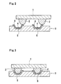
- the bump 2 on the semiconductor device 1 is positioned to the electrode terminal 5 on the substrate by a positioning machine (not shown). This positioning may be coarse to assure that a portion of the bump 2 abuts the metal layer 6 as shown in Fig. 2, because when the substrate 3 is heated after the positioning to melt only the metal layer 6, the molten metal layer material contracts by the surface tension, and if the top of the bump 2 is on the metal layer 6, the bump 2 is induced into the recess 4 by the surface tension and it is exactly positioned to the electrode terminal 5 as shown in Fig. 3.
- the surface tension functions to minimize a surface area of the metal layer material between the electrode pad (not shown) on the semiconductor device on which the bump 2 is formed and the electrode terminal 5 on the substrate 3. Accordingly, the semiconductor device 1 is positioned to the substrate 3 by the surface tension such that a total positional error between the electrode pad on the semiconductor device 1 and the electrode terminal 5 on the substrate 3 is minimized. After such exact positioning, the substrate 3 may be further heated to melt the bump 2 to interconnect the bump 2 and the electrode terminal 5, or the bump 2 may not be molten but it may be connected by the molten metal layer material.
- the size of the bump 2 formed on the semiconductor device 1 was 80 ⁇ m in diameter and approximately 30 ⁇ m in height.
- a size of the electrode terminal 5 on the substrate 3 was 100 ⁇ m in diameter.
- the metal layer 6 was formed on the entire surface of the electrode terminal 5 and the semiconductor device 1 was packaged on the substrate 3. In this case, a positioning precision required for the positioning machine in order to keep the positional error between the bump 2 and the electrode terminal 5 after the packaging within ⁇ 10 ⁇ m was ⁇ 50 ⁇ m.
- the same semiconductor device as that of the above example was packaged on a prior art substrate having a flat electrode terminal of the same dimension as that of the above example.
- the precision required for the positioning machine was +/- 10 ⁇ m. The result is shown below.
- a plurality of bumps 2 are formed on the surface of the semiconductor device 1 to project therefrom.
- a plurality of electrode terminals 5 corresponding to the bumps on the semiconductor devices 1 are formed on the substrate 3 to which the semiconductor device 1 is to be packaged.
- Each of the electrode terminals 5 has a recess 4 formed thereon to receive at least a top of the bump 2.
- the recess 4 is formed in such a manner that the depth thereof gradually increases as it goes from the periphery to the center so that it is deepest at the center.
- the electrode terminal 5 may, for example, be formed in the following manner. First, a recess is formed at an area of the substrate 3 at which the electrode terminal 5 is to be formed.
- the recess is formed to have an enough size to receive at least the top of the bump 2 formed on the semiconductor device 1.
- the recess is selectively metal-plated or vacuum-deposited to form the electrode terminal 5.
- the electrode terminal 5 thus formed has the recess 4 for receiving at least the top of the bump 2 formed thereon.
- a center 5a and periphery 5b of the electrode terminal 5 are separately formed, and the center 5a is made of a metal having a lower melting point than that of the periphery 5b.
- the center 5a is made of an alloy of Au/20%Sn, and the periphery 5b is made of Au.
- the bump 2 on the semiconductor device 1 is positioned to the electrode terminal 5 on the substrate by a positioning machine (not shown). This positioning may be coarse to assure that a portion of the bump 2 is placed within the recess 4 as shown in Fig. 4. Because if the top of the bump 2 is positioned within a range of the recess 4 of the electrode terminal 5, the bump 2 is guided along the surface of the recess 4 of the electrode terminal 5 by lightly pushing the semiconductor device 1 to the substrate 3 after the positioning and it is automatically moved toward the center of the recess 4. However, since a frictional force acts between the bump 2 and the electrode terminal 5, the bump 2 stops at a position slightly deviated from the center of the electrode terminal 5.
- the center 5a of the electrode terminal 5 is made of the low melting point metal to cover the position at which the bump 2 stops, a surface tension of the molten metal acts to the bump 2 by heating the substrate 3 and melting the center 5a of the electrode terminal 5 and the bump 2 is further induced into the center of the electrode terminal 5 by the surface tension.
- the bump 2 is positioned to the center of the electrode terminal 5 very precisely.
- the surface tension functions to minimize the surface area of the molten metal.
- the semiconductor device is positioned to the substrate 3 by the surface tension so that the total positional error between the bump 2 on the semiconductor device 1 and the electrode terminal 5 on the substrate 3 is minimized. After such precise positioning, the substrate 3 may be further heated to melt the bump 2 to connect the bump 2 and the electrode terminal 5.
- the size of the bump 2 formed on the semiconductor device 1 was 80 ⁇ m in diameter and approximately 30 ⁇ m in height.
- a size of the electrode terminal 5 on the substrate 3 was 100 ⁇ m in diameter.
- the semiconductor device 1 was packaged on the substrate 3.
- a positioning precision required for the positioning machine in order to keep the positional error between the bump 2 and the electrode terminal 5 after the packaging within ⁇ 5 ⁇ m was ⁇ 50 ⁇ m.
- the same semiconductor device as that of the above example was packaged on a prior art substrate having a flat electrode terminal of the same dimension as that of the above example.
- the precision required for the positioning machine was +/- 5 ⁇ m. The result is shown below.
- a coolant such as a cooling gas is blown into the surface on the electrode terminal 5 of the packaging substrate 3 when the substrate is heated to make difference from above described embodiment.
- the packaging substrate 3 is heated by a hot plate 6, the control of temperature is very difficult to attain.
- the entire electrode terminal 5 may be molten or the wiring other than the electrode may be molten. If the area other than the center 5a of the electrode terminal 5 is molten, the surface tension does not function in the manner described above and the bump 2 may not come to the center of the recess of the electrode terminal 5 or the molten electrode material may swell out to shorten an adjacent electrode.
- the packaging substrate 3 is heated while cooling gas is blown to the surface of the packaging substrate 3 on which the electrode terminal 5 is formed (Fig. 7).
- cooling gas By cooling the surface of the packaging substrate by flowing the gas, it is possible to increase a temperature gradient on the surface of the packaging substrate 3.
- the center 5a of the electrode terminal 5 is recessed, it is hardly blown by the cooling gas.
- it is on a high temperature side of the temperature gradient only the recessed center of the electrode terminal 5 reaches a high temperature compared to other areas. Accordingly, only the low melting point metal of the center 5a of the electrode terminal 5 is molten (Fig.
- the cooling gas is preferably inert gas such as N2 gas. Since the packaging substrate 3 and the semiconductor device 1 face each other as shown in Fig. 7 and 8, the blowing is done to blow the gas into a gap between the semiconductor device 1 and the packaging substrate 3 from the side of the packaging substrate.
- a temperature of the cooling gas blown to the packaging substrate 3 may be a room temperature, but if the temperature and the blow rate of the gas are controllable, the temperature on the surface of the packaging substrate 3 can be controlled.
Abstract
Description
- The present invention relates to a substrate for packaging a semiconductor device such as an IC chip.
- In packaging a semiconductor device such as an IC, it has been practiced to form a convex bump on an electrode pad of the semiconductor device and directly connect the bump to an electrode terminal formed on the substrate.
- In the past, the electrode terminal on the substrate has been formed flat. Thus, if the bump on the semiconductor device is not exactly positioned at the material will swell out to a periphery of the electrode terminal and may shorten the adjacent electrode terminals.
- Further, the higher the interaction density of the semiconductor device is, the smaller are the size and pitch of the electrode terminals formed on the substrate. As a result, as the integration density goes higher, it is necessary to more precisely position the bump to the electrode terminal.
- However, such a high precision positioning requires a longer time, and the packaging time increases and a high precision and expensive positioning machine is required. As a result, the packaging cost increases.
- It is an object of the present invention to shorten the time required for packaging and reduce the packaging cost.
- In order to achieve the above object, in the substrate for packaging the semiconductor device of the present invention, a recess for receiving at least a top of a bump on the semiconductor device is formed in an electrode terminal on the substrate, and at least the recess of the surface of the electrode terminal is covered by conductive member such as a metal layer having a lower melting point than that of the bump.
- By melting conductive member such as a low melting point metal layer on the surface of the electrode terminal after coarse positioning, the bump on the semiconductor device is induced into the recess of the electrode terminal by a surface tension of the conductive member such as a low melting point metal so that the bump is exactly positioned for the electrode terminal. And the substrate for packaging the semiconductor device of the present invention, a recess for receiving at least a top of a bump is formed on the surface of the electrode terminal on the substrate in such a manner that a depth of the recess increases as it goes from a periphery to a center, and the center of the recess of the electrode terminal is made of a conductive member such as a metal having a lower melting point than that of the periphery.
- By merely pushing the semiconductor device to the substrate the coarse positioning, the bump on the semiconductor device is precisely positioned to the electrode terminal on the substrate. Further, by melting the conductive member such as a low melting point metal at the center of the recess of the electrode terminal, the bump on the semiconductor device is induced into the center of the electrode terminal on the substrate by the surface tension of the low melting point metal so that the bump and the electrode terminal are positioned more precisely. Further, in the method for packaging the semiconductor device of the present invention, a recess for receiving a top of a bump on the semiconductor device is formed in an electrode terminal on the packaging substrate, a conductive member such as a low melting point metal is arranged at at least center of the recess, and the packaging substrate is heated while cooling gas is blown to the surface of the packaging substrate.
- By merely pushing the semiconductor device to the packaging substrate after the coarse positioning, the bump on the semiconductor device can be precisely positioned to the electrode terminal on the packaging substrate. Further, since only the conductive member such as a low melting point metal at the center of the recess of the electrode terminal can be molten, the bump on the semiconductor device is induced into the center of the electrode terminal on the molten low melting point metal and the bump is more precisely positioned to the electrode terminal.
- The present invention will become more fully understood from the detailed description given hereinbelow and the accompanying drawings which are given by way of illustration only, and thus are not to be considered as limiting the present invention.
- Further scope of applicability of the present invention will become apparent from the detailed description given hereinafter. However, it should be understood that the detailed description and specific examples, while indicating preferred embodiments of the invention, are given by way of illustration only, since various changes and modifications within the spirit and scope of the invention will become apparent to those skilled in the art from this detailed description.
-
- Fig. 1A and 1B show a process for connection of a semiconductor device to a packaging substrate according to the first embodiment of the present invention,
- Fig. 2 shows a semiconductor device having coarsely positioned to an electrode terminal of a substrate according to the first embodiment for packaging the semiconductor device in cross section on the perpendicular direction to the substrate surface,
- Fig. 3 shows a structure according to the first embodiment after the packaging in cross section on the perpendicular direction to the substrate surface,
- Fig. 4 shows a semiconductor device having coarsely positioned to an electrode terminal of a substrate according to the second embodiment for packaging the semiconductor device in cross section on the perpendicular direction to the substrate surface,
- Fig. 5 shows an intermediate position of movement of a bump on the semiconductor device to a center of the electrode terminal on the substrate according to the second embodiment in cross section on the perpendicular direction to the substrate surface,
- Fig. 6 shows a structure according to the second embodiment after packaging in cross section on the perpendicular direction to the substrate surface,
- Fig. 7 shows a semiconductor device having coarsely positioned to an electrode terminal of a packaging substrate in accordance with the third embodiment in cross section on the perpendicular direction to the substrate surface.
- Fig. 8 shows an intermediate position of the movement of a bump on the semiconductor device to a center of the electrode terminal on the packaging substrate according to the third embodiment in cross section of a perpendicular to the substrate, and
- Fig. 9 shows a structure according to the third embodiment after the packaging in cross section of a perpendicular to the substrate.
- The first embodiment of the present invention is now described with reference to Figs. 1 to 3.
- As shown in Figs. 1A and 1B, a plurality of
bumps 2 are formed on the surface of thesemiconductor device 1 to project therefrom. - On the other hand, a plurality of
electrode terminals 5 corresponding to the bumps on thesemiconductor devices 1 are formed on thesubstrate 3 to which thesemiconductor device 1 is to be packaged. Each of theelectrode terminals 5 has arecess 4 formed thereon to receive at least a top of thebump 2. Theelectrode terminal 5 may, for example, be formed in the following manner. First, a recess is formed at an area of thesubstrate 3 at which theelectrode terminal 5 is to be formed. The recess is large enough to receive at least the top (bottom in the drawing) of thebump 2 formed on thesemiconductor device 1. The recess is selectively plated to form theelectrode terminal 5. Theelectrode terminal 5 thus formed has therecess 4 for receiving at least the top of thebump 2 on the surface thereof. At least therecess 4 of the surface of theelectrode 5 is covered by a metal layer 6 made of a metal (for example, Au/20%Sn, Pb/40%In) having a lower melting point than those of thebump 2 and theelectrode terminal 5. The metal layer 6 is formed by a vacuum deposition method. It is preferable that a center of theelectrode terminal 5 coincides to a deepest (lowest) position of therecess 4. - When the
semiconductor device 1 is to be packaged to thesubstrate 3 thus formed, thebump 2 on thesemiconductor device 1 is positioned to theelectrode terminal 5 on the substrate by a positioning machine (not shown). This positioning may be coarse to assure that a portion of thebump 2 abuts the metal layer 6 as shown in Fig. 2, because when thesubstrate 3 is heated after the positioning to melt only the metal layer 6, the molten metal layer material contracts by the surface tension, and if the top of thebump 2 is on the metal layer 6, thebump 2 is induced into therecess 4 by the surface tension and it is exactly positioned to theelectrode terminal 5 as shown in Fig. 3. The surface tension functions to minimize a surface area of the metal layer material between the electrode pad (not shown) on the semiconductor device on which thebump 2 is formed and theelectrode terminal 5 on thesubstrate 3. Accordingly, thesemiconductor device 1 is positioned to thesubstrate 3 by the surface tension such that a total positional error between the electrode pad on thesemiconductor device 1 and theelectrode terminal 5 on thesubstrate 3 is minimized. After such exact positioning, thesubstrate 3 may be further heated to melt thebump 2 to interconnect thebump 2 and theelectrode terminal 5, or thebump 2 may not be molten but it may be connected by the molten metal layer material. - The size of the
bump 2 formed on thesemiconductor device 1 was 80 µm in diameter and approximately 30 µm in height. A size of theelectrode terminal 5 on thesubstrate 3 was 100 µm in diameter. The metal layer 6 was formed on the entire surface of theelectrode terminal 5 and thesemiconductor device 1 was packaged on thesubstrate 3. In this case, a positioning precision required for the positioning machine in order to keep the positional error between thebump 2 and theelectrode terminal 5 after the packaging within ± 10 µm was ± 50µm. - On the other hand, the same semiconductor device as that of the above example was packaged on a prior art substrate having a flat electrode terminal of the same dimension as that of the above example. The precision required for the positioning machine was +/- 10µm. The result is shown below.

- Next, the second embodiment of the present invention is now described with reference to Figs. 4, 5 and 6.
- As shown, a plurality of
bumps 2 are formed on the surface of thesemiconductor device 1 to project therefrom. - On the other hand, a plurality of
electrode terminals 5 corresponding to the bumps on thesemiconductor devices 1 are formed on thesubstrate 3 to which thesemiconductor device 1 is to be packaged. Each of theelectrode terminals 5 has arecess 4 formed thereon to receive at least a top of thebump 2. Therecess 4 is formed in such a manner that the depth thereof gradually increases as it goes from the periphery to the center so that it is deepest at the center. Theelectrode terminal 5 may, for example, be formed in the following manner. First, a recess is formed at an area of thesubstrate 3 at which theelectrode terminal 5 is to be formed. - The recess is formed to have an enough size to receive at least the top of the
bump 2 formed on thesemiconductor device 1. The recess is selectively metal-plated or vacuum-deposited to form theelectrode terminal 5. Theelectrode terminal 5 thus formed has therecess 4 for receiving at least the top of thebump 2 formed thereon. Acenter 5a andperiphery 5b of theelectrode terminal 5 are separately formed, and thecenter 5a is made of a metal having a lower melting point than that of theperiphery 5b. In the present embodiment, thecenter 5a is made of an alloy of Au/20%Sn, and theperiphery 5b is made of Au. - When the
semiconductor device 1 is to be packaged to thesubstrate 3 thus formed, thebump 2 on thesemiconductor device 1 is positioned to theelectrode terminal 5 on the substrate by a positioning machine (not shown). This positioning may be coarse to assure that a portion of thebump 2 is placed within therecess 4 as shown in Fig. 4. Because if the top of thebump 2 is positioned within a range of therecess 4 of theelectrode terminal 5, thebump 2 is guided along the surface of therecess 4 of theelectrode terminal 5 by lightly pushing thesemiconductor device 1 to thesubstrate 3 after the positioning and it is automatically moved toward the center of therecess 4. However, since a frictional force acts between thebump 2 and theelectrode terminal 5, thebump 2 stops at a position slightly deviated from the center of theelectrode terminal 5. Thecenter 5a of theelectrode terminal 5 is made of the low melting point metal to cover the position at which thebump 2 stops, a surface tension of the molten metal acts to thebump 2 by heating thesubstrate 3 and melting thecenter 5a of theelectrode terminal 5 and thebump 2 is further induced into the center of theelectrode terminal 5 by the surface tension. Accordingly, as shown in Fig. 6, thebump 2 is positioned to the center of theelectrode terminal 5 very precisely. The surface tension functions to minimize the surface area of the molten metal. Accordingly the semiconductor device is positioned to thesubstrate 3 by the surface tension so that the total positional error between thebump 2 on thesemiconductor device 1 and theelectrode terminal 5 on thesubstrate 3 is minimized. After such precise positioning, thesubstrate 3 may be further heated to melt thebump 2 to connect thebump 2 and theelectrode terminal 5. - The size of the
bump 2 formed on thesemiconductor device 1 was 80 µm in diameter and approximately 30 µm in height. A size of theelectrode terminal 5 on thesubstrate 3 was 100 µm in diameter. Thesemiconductor device 1 was packaged on thesubstrate 3. In this case, a positioning precision required for the positioning machine in order to keep the positional error between thebump 2 and theelectrode terminal 5 after the packaging within ± 5 µm was ± 50 µm. On the other hand, the same semiconductor device as that of the above example was packaged on a prior art substrate having a flat electrode terminal of the same dimension as that of the above example. The precision required for the positioning machine was +/- 5 µm. The result is shown below.
- Next, the third embodiment of the present invention will be explained in reference with Figs. 7 to 9. In this embodiment, a coolant such as a cooling gas is blown into the surface on the
electrode terminal 5 of thepackaging substrate 3 when the substrate is heated to make difference from above described embodiment. Where thepackaging substrate 3 is heated by a hot plate 6, the control of temperature is very difficult to attain. When thepackaging substrate 3 is heated, theentire electrode terminal 5 may be molten or the wiring other than the electrode may be molten. If the area other than thecenter 5a of theelectrode terminal 5 is molten, the surface tension does not function in the manner described above and thebump 2 may not come to the center of the recess of theelectrode terminal 5 or the molten electrode material may swell out to shorten an adjacent electrode. In order to avoid such problems, in the present invention, thepackaging substrate 3 is heated while cooling gas is blown to the surface of thepackaging substrate 3 on which theelectrode terminal 5 is formed (Fig. 7). By cooling the surface of the packaging substrate by flowing the gas, it is possible to increase a temperature gradient on the surface of thepackaging substrate 3. In this case, since thecenter 5a of theelectrode terminal 5 is recessed, it is hardly blown by the cooling gas. Further, since it is on a high temperature side of the temperature gradient, only the recessed center of theelectrode terminal 5 reaches a high temperature compared to other areas. Accordingly, only the low melting point metal of thecenter 5a of theelectrode terminal 5 is molten (Fig. 8) and thebump 2 is induced into the center of theelectrode terminal 5 by a surface tension (Fig. 9). The cooling gas is preferably inert gas such as N₂ gas. Since thepackaging substrate 3 and thesemiconductor device 1 face each other as shown in Fig. 7 and 8, the blowing is done to blow the gas into a gap between thesemiconductor device 1 and thepackaging substrate 3 from the side of the packaging substrate. A temperature of the cooling gas blown to thepackaging substrate 3 may be a room temperature, but if the temperature and the blow rate of the gas are controllable, the temperature on the surface of thepackaging substrate 3 can be controlled. - From the invention thus described, it will be obvious that the invention may be varied in many ways. Such variations are not to be regarded as a departure from the spirit and scope of the invention, and all such modifications as would be obvious to one skilled in the art are intended to be included within the scope of the following claims.
Claims (19)
- A substrate for packaging a semiconductor device having a bump projecting from a surface thereof,
Wherein said substrate has an electrode terminal to which said bump is to be connected, a recess for receiving at least a top of said bump is formed on a surface of said electrode terminal, and a conductive member having a lower melting point than that of said bump is formed on said recess. - A substrate for packaging a semiconductor device according to Claim 1 wherein said conductive member is a metal layer.
- A substrate for packaging a semiconductor device according to Claim 2 wherein said metal layer is coated on the surface of said recess.
- A substrate for packaging a semiconductor device according to Claim 2 wherein said recess is of substantially sphere shape having a larger radius of curvature than that of said top of said bump.
- A substrate for packaging a semiconductor device having a bump projecting from a surface thereof,
wherein said substrate has an electrode terminal to which said bump is to be connected, a recess for accepting at least a top of said bump is formed on a surface of said electrode terminal in such a manner that a depth of said recess increases as it goes from a periphery to a center, and a conductive member of a lower melting point than that of the periphery is formed at the center of the recess of said electrode terminal. - A substrate for packaging a semiconductor device according to Claim 5 wherein said conductive member is a metal layer.
- A substrate for packaging a semiconductor device having a bump projecting from a surface thereof,
wherein said substrate has a recess formed thereon for receiving at least a top of said bump, an electrode terminal is formed in said recess and a center of said electrode terminal is made of a material having a lower melting point than that of a material of a periphery. - A substrate for packaging a semiconductor device according to Claim 7 wherein said electrode terminal is formed by selective plating.
- A packaging structure of a semiconductor device comprising:
a semiconductor device having a bump projecting from a surface thereof; and
a packaging substrate having an electrode terminal to which said bump is to be connected wherein a recess for receiving at least a top of said bump is formed on the surface of said electrode terminal, and a conductive material of a lower melting point than that of said bump is formed on said recess. - A packaging structure of a semiconductor device according to Claim 9 wherein said conductive member is coated on the surface of said recess.
- A packaging structure of a semiconductor device according to Claim 9 wherein said conductive member is formed at a center of said recess and a member of a lower melting point than that of said conductive member is formed in a periphery.
- A packaging structure of a semiconductor device according to Claim 9 wherein the top of said bump is of substantially sphere shape and said recess has a larger radius of curvature than that of said top of said bump.
- A method for packaging a semiconductor device on a packaging substrate by directly connecting a bump formed on a surface of said semiconductor device to an electrode terminal on said packaging substrate comprising the steps of:
forming a recess for receiving a top of said bump in said electrode terminal and arranging a low melting point conductive member having a lower melting point than that of a periphery of said recess at a center of said recess; and heating said low melting point conductive member to melt said low melting point conductive member. - A method for packaging a semiconductor device according to Claim 13 further comprising the step of heating said packaging substrate to melt said low melting point conductive member while flowing coolant to the surface of said packaging substrate to cool the surface of said packaging substrate.
- A method for packaging a semiconductor device according to Claim 13 wherein said low melting point conductive member is a metal and said coolant is cooling gas.
- A method for packaging a semiconductor device on a packaging substrate by directly connecting a bump formed on a surface of said semiconductor device to an electrode terminal on said packaging substrate, comprising the steps of:
preparing the packaging substrate having a low melting point conductive member of a lower melting point than that of a periphery thereof formed at least center thereof and the electrode terminal for receiving a top of said bump by said recess;
positioning the top of said bump within a range of said recess;
pushing said semiconductor device and/or said packaging substrate to contact the top of said bump to said low melting point conductive member, and
heating said low melting point conductive member to melt the same and moving said bump to the center of said recess by a surface tension of the molten low melting point conductive material. - A method for packaging a semiconductor device according to Claim 16 further comprising the step of heating said packaging substrate to melt said low melting point conductive member while blowing coolant to the surface of said packaging substrate to cool the surface of said packaging substrate.
- A method for packaging a semiconductor device according to Claim 17 wherein said low melting point conductive member is a metal and said coolant is cooling gas.
- A packaging structure of a semiconductor device comprising:
a packaging substrate having a bump projecting from a surface thereof; and
a semiconductor device having an electrode pad to which said bump is to be connected wherein a recess for receiving at least a top of said bump is formed on the surface of said electrode terminal, and a conductive material of a lower melting point than that of said bump is formed on said recess.
Applications Claiming Priority (6)
| Application Number | Priority Date | Filing Date | Title |
|---|---|---|---|
| JP13415/90 | 1990-01-23 | ||
| JP13414/90 | 1990-01-23 | ||
| JP2013415A JPH03218037A (en) | 1990-01-23 | 1990-01-23 | Semiconductor element mounting board |
| JP13416/90 | 1990-01-23 | ||
| JP2013416A JPH03218038A (en) | 1990-01-23 | 1990-01-23 | Mounting method of semiconductor element |
| JP2013414A JPH03218036A (en) | 1990-01-23 | 1990-01-23 | Semiconductor element mounting board |
Publications (2)
| Publication Number | Publication Date |
|---|---|
| EP0439137A2 true EP0439137A2 (en) | 1991-07-31 |
| EP0439137A3 EP0439137A3 (en) | 1994-01-05 |
Family
ID=27280243
Family Applications (1)
| Application Number | Title | Priority Date | Filing Date |
|---|---|---|---|
| EP91100821A Withdrawn EP0439137A2 (en) | 1990-01-23 | 1991-01-23 | Substrate for packaging a semiconductor device, packaging structure and method |
Country Status (5)
| Country | Link |
|---|---|
| US (2) | US5196726A (en) |
| EP (1) | EP0439137A2 (en) |
| KR (1) | KR950001368B1 (en) |
| AU (1) | AU637874B2 (en) |
| CA (1) | CA2034700A1 (en) |
Cited By (2)
| Publication number | Priority date | Publication date | Assignee | Title |
|---|---|---|---|---|
| DE19541039A1 (en) * | 1995-11-03 | 1997-05-07 | David Finn | Chip module e.g. for chip card |
| GB2325354A (en) * | 1997-03-26 | 1998-11-18 | Whitaker Corp | Electrical connector or connection with concave ball-receiving site |
Families Citing this family (146)
| Publication number | Priority date | Publication date | Assignee | Title |
|---|---|---|---|---|
| AU645283B2 (en) * | 1990-01-23 | 1994-01-13 | Sumitomo Electric Industries, Ltd. | Substrate for packaging a semiconductor device |
| WO1993015424A1 (en) * | 1992-01-28 | 1993-08-05 | British Telecommunications Public Limited Company | Alignment of integrated optical components |
| US5821627A (en) * | 1993-03-11 | 1998-10-13 | Kabushiki Kaisha Toshiba | Electronic circuit device |
| US5477086A (en) * | 1993-04-30 | 1995-12-19 | Lsi Logic Corporation | Shaped, self-aligning micro-bump structures |
| US5767580A (en) * | 1993-04-30 | 1998-06-16 | Lsi Logic Corporation | Systems having shaped, self-aligning micro-bump structures |
| US6414506B2 (en) | 1993-09-03 | 2002-07-02 | Micron Technology, Inc. | Interconnect for testing semiconductor dice having raised bond pads |
| US5632631A (en) * | 1994-06-07 | 1997-05-27 | Tessera, Inc. | Microelectronic contacts with asperities and methods of making same |
| US5615824A (en) * | 1994-06-07 | 1997-04-01 | Tessera, Inc. | Soldering with resilient contacts |
| US5802699A (en) * | 1994-06-07 | 1998-09-08 | Tessera, Inc. | Methods of assembling microelectronic assembly with socket for engaging bump leads |
| US5983492A (en) * | 1996-11-27 | 1999-11-16 | Tessera, Inc. | Low profile socket for microelectronic components and method for making the same |
| JP3377867B2 (en) * | 1994-08-12 | 2003-02-17 | 京セラ株式会社 | Package for storing semiconductor elements |
| US6826827B1 (en) * | 1994-12-29 | 2004-12-07 | Tessera, Inc. | Forming conductive posts by selective removal of conductive material |
| DE19510003A1 (en) * | 1995-03-22 | 1996-09-26 | Inst Mikrotechnik Mainz Gmbh | Semiconductor platelet on support precise location method |
| US5872051A (en) * | 1995-08-02 | 1999-02-16 | International Business Machines Corporation | Process for transferring material to semiconductor chip conductive pads using a transfer substrate |
| US5810609A (en) | 1995-08-28 | 1998-09-22 | Tessera, Inc. | Socket for engaging bump leads on a microelectronic device and methods therefor |
| JP2845847B2 (en) * | 1996-11-12 | 1999-01-13 | 九州日本電気株式会社 | Semiconductor integrated circuit |
| JPH10260223A (en) | 1997-03-19 | 1998-09-29 | Fujitsu Ltd | Semiconductor inspection device and inspection method using the same |
| US6016060A (en) * | 1997-03-25 | 2000-01-18 | Micron Technology, Inc. | Method, apparatus and system for testing bumped semiconductor components |
| US5962921A (en) | 1997-03-31 | 1999-10-05 | Micron Technology, Inc. | Interconnect having recessed contact members with penetrating blades for testing semiconductor dice and packages with contact bumps |
| US5880590A (en) * | 1997-05-07 | 1999-03-09 | International Business Machines Corporation | Apparatus and method for burn-in and testing of devices with solder bumps or preforms |
| JPH113953A (en) * | 1997-06-10 | 1999-01-06 | Fujitsu Ltd | Semiconductor device and manufacture thereof |
| US6040702A (en) * | 1997-07-03 | 2000-03-21 | Micron Technology, Inc. | Carrier and system for testing bumped semiconductor components |
| US6072326A (en) * | 1997-08-22 | 2000-06-06 | Micron Technology, Inc. | System for testing semiconductor components |
| US6096576A (en) | 1997-09-02 | 2000-08-01 | Silicon Light Machines | Method of producing an electrical interface to an integrated circuit device having high density I/O count |
| US6018249A (en) * | 1997-12-11 | 2000-01-25 | Micron Technolgoy, Inc. | Test system with mechanical alignment for semiconductor chip scale packages and dice |
| US6200143B1 (en) | 1998-01-09 | 2001-03-13 | Tessera, Inc. | Low insertion force connector for microelectronic elements |
| US6040630A (en) * | 1998-04-13 | 2000-03-21 | Harris Corporation | Integrated circuit package for flip chip with alignment preform feature and method of forming same |
| US6337577B1 (en) | 1998-05-11 | 2002-01-08 | Micron Technology, Inc. | Interconnect and system for testing bumped semiconductor components with on-board multiplex circuitry for expanding tester resources |
| US6677776B2 (en) * | 1998-05-11 | 2004-01-13 | Micron Technology, Inc. | Method and system having switching network for testing semiconductor components on a substrate |
| US6303986B1 (en) | 1998-07-29 | 2001-10-16 | Silicon Light Machines | Method of and apparatus for sealing an hermetic lid to a semiconductor die |
| US6235630B1 (en) * | 1998-08-19 | 2001-05-22 | Micron Technology, Inc. | Silicide pattern structures and methods of fabricating the same |
| US6819127B1 (en) | 1999-02-19 | 2004-11-16 | Micron Technology, Inc. | Method for testing semiconductor components using interposer |
| US6242932B1 (en) | 1999-02-19 | 2001-06-05 | Micron Technology, Inc. | Interposer for semiconductor components having contact balls |
| US6980017B1 (en) | 1999-03-10 | 2005-12-27 | Micron Technology, Inc. | Test interconnect for bumped semiconductor components and method of fabrication |
| US6222280B1 (en) | 1999-03-22 | 2001-04-24 | Micron Technology, Inc. | Test interconnect for semiconductor components having bumped and planar contacts |
| US6437591B1 (en) | 1999-03-25 | 2002-08-20 | Micron Technology, Inc. | Test interconnect for bumped semiconductor components and method of fabrication |
| US6396291B1 (en) | 1999-04-23 | 2002-05-28 | Micron Technology, Inc. | Method for testing semiconductor components |
| US6313999B1 (en) | 1999-06-10 | 2001-11-06 | Agere Systems Optoelectronics Guardian Corp. | Self alignment device for ball grid array devices |
| US6285203B1 (en) | 1999-06-14 | 2001-09-04 | Micron Technology, Inc. | Test system having alignment member for aligning semiconductor components |
| US6316737B1 (en) * | 1999-09-09 | 2001-11-13 | Vlt Corporation | Making a connection between a component and a circuit board |
| JP3822040B2 (en) * | 2000-08-31 | 2006-09-13 | 株式会社ルネサステクノロジ | Electronic device and manufacturing method thereof |
| US6747781B2 (en) | 2001-06-25 | 2004-06-08 | Silicon Light Machines, Inc. | Method, apparatus, and diffuser for reducing laser speckle |
| US6782205B2 (en) | 2001-06-25 | 2004-08-24 | Silicon Light Machines | Method and apparatus for dynamic equalization in wavelength division multiplexing |
| US6829092B2 (en) | 2001-08-15 | 2004-12-07 | Silicon Light Machines, Inc. | Blazed grating light valve |
| JP2003124416A (en) * | 2001-10-16 | 2003-04-25 | Yazaki Corp | Joint structure between chip part and bus bar |
| US6750546B1 (en) * | 2001-11-05 | 2004-06-15 | Skyworks Solutions, Inc. | Flip-chip leadframe package |
| US6674647B2 (en) * | 2002-01-07 | 2004-01-06 | International Business Machines Corporation | Low or no-force bump flattening structure and method |
| US6800238B1 (en) | 2002-01-15 | 2004-10-05 | Silicon Light Machines, Inc. | Method for domain patterning in low coercive field ferroelectrics |
| JP3888439B2 (en) * | 2002-02-25 | 2007-03-07 | セイコーエプソン株式会社 | Manufacturing method of semiconductor device |
| US6767751B2 (en) | 2002-05-28 | 2004-07-27 | Silicon Light Machines, Inc. | Integrated driver process flow |
| US6822797B1 (en) | 2002-05-31 | 2004-11-23 | Silicon Light Machines, Inc. | Light modulator structure for producing high-contrast operation using zero-order light |
| US6829258B1 (en) | 2002-06-26 | 2004-12-07 | Silicon Light Machines, Inc. | Rapidly tunable external cavity laser |
| US6714337B1 (en) | 2002-06-28 | 2004-03-30 | Silicon Light Machines | Method and device for modulating a light beam and having an improved gamma response |
| US6813059B2 (en) | 2002-06-28 | 2004-11-02 | Silicon Light Machines, Inc. | Reduced formation of asperities in contact micro-structures |
| WO2004006178A1 (en) * | 2002-07-03 | 2004-01-15 | Quelis Id Systems Inc. | Wire positioning and mechanical attachment for a radio-frequency identification device |
| US20040030766A1 (en) * | 2002-08-12 | 2004-02-12 | Michael Witkowski | Method and apparatus for switch fabric configuration |
| US6801354B1 (en) | 2002-08-20 | 2004-10-05 | Silicon Light Machines, Inc. | 2-D diffraction grating for substantially eliminating polarization dependent losses |
| US6642158B1 (en) * | 2002-09-23 | 2003-11-04 | Intel Corporation | Photo-thermal induced diffusion |
| US6712480B1 (en) | 2002-09-27 | 2004-03-30 | Silicon Light Machines | Controlled curvature of stressed micro-structures |
| US6806997B1 (en) | 2003-02-28 | 2004-10-19 | Silicon Light Machines, Inc. | Patterned diffractive light modulator ribbon for PDL reduction |
| US6829077B1 (en) | 2003-02-28 | 2004-12-07 | Silicon Light Machines, Inc. | Diffractive light modulator with dynamically rotatable diffraction plane |
| JP3772983B2 (en) * | 2003-03-13 | 2006-05-10 | セイコーエプソン株式会社 | Manufacturing method of electronic device |
| US7462936B2 (en) | 2003-10-06 | 2008-12-09 | Tessera, Inc. | Formation of circuitry with modification of feature height |
| US8641913B2 (en) * | 2003-10-06 | 2014-02-04 | Tessera, Inc. | Fine pitch microcontacts and method for forming thereof |
| US7495179B2 (en) | 2003-10-06 | 2009-02-24 | Tessera, Inc. | Components with posts and pads |
| US7709968B2 (en) * | 2003-12-30 | 2010-05-04 | Tessera, Inc. | Micro pin grid array with pin motion isolation |
| WO2005065207A2 (en) | 2003-12-30 | 2005-07-21 | Tessera, Inc. | Microelectronic packages and methods therefor |
| US8207604B2 (en) * | 2003-12-30 | 2012-06-26 | Tessera, Inc. | Microelectronic package comprising offset conductive posts on compliant layer |
| US20050208749A1 (en) * | 2004-03-17 | 2005-09-22 | Beckman Michael W | Methods for forming electrical connections and resulting devices |
| US7453157B2 (en) * | 2004-06-25 | 2008-11-18 | Tessera, Inc. | Microelectronic packages and methods therefor |
| WO2006004671A2 (en) * | 2004-06-25 | 2006-01-12 | Tessera, Inc. | Microelectronic package structure with spherical contact pins |
| JP4359257B2 (en) * | 2004-07-06 | 2009-11-04 | 三星電機株式会社 | BGA package and manufacturing method thereof |
| KR101313391B1 (en) | 2004-11-03 | 2013-10-01 | 테세라, 인코포레이티드 | Stacked packaging improvements |
| US7939934B2 (en) * | 2005-03-16 | 2011-05-10 | Tessera, Inc. | Microelectronic packages and methods therefor |
| US7618844B2 (en) * | 2005-08-18 | 2009-11-17 | Intelleflex Corporation | Method of packaging and interconnection of integrated circuits |
| US8058101B2 (en) | 2005-12-23 | 2011-11-15 | Tessera, Inc. | Microelectronic packages and methods therefor |
| US8067267B2 (en) * | 2005-12-23 | 2011-11-29 | Tessera, Inc. | Microelectronic assemblies having very fine pitch stacking |
| KR100755658B1 (en) * | 2006-03-09 | 2007-09-04 | 삼성전기주식회사 | Light emitting diode package |
| JP5050384B2 (en) | 2006-03-31 | 2012-10-17 | 富士通セミコンダクター株式会社 | Semiconductor device and manufacturing method thereof |
| US7545029B2 (en) * | 2006-08-18 | 2009-06-09 | Tessera, Inc. | Stack microelectronic assemblies |
| US20080150101A1 (en) * | 2006-12-20 | 2008-06-26 | Tessera, Inc. | Microelectronic packages having improved input/output connections and methods therefor |
| US7692281B2 (en) * | 2007-02-16 | 2010-04-06 | Tyco Electronics Corporation | Land grid array module with contact locating features |
| US7868457B2 (en) * | 2007-09-14 | 2011-01-11 | International Business Machines Corporation | Thermo-compression bonded electrical interconnect structure and method |
| US8043893B2 (en) | 2007-09-14 | 2011-10-25 | International Business Machines Corporation | Thermo-compression bonded electrical interconnect structure and method |
| US8558379B2 (en) | 2007-09-28 | 2013-10-15 | Tessera, Inc. | Flip chip interconnection with double post |
| US20090243100A1 (en) * | 2008-03-27 | 2009-10-01 | Jotaro Akiyama | Methods to Form a Three-Dimensionally Curved Pad in a Substrate and Integrated Circuits Incorporating such a Substrate |
| US20100044860A1 (en) * | 2008-08-21 | 2010-02-25 | Tessera Interconnect Materials, Inc. | Microelectronic substrate or element having conductive pads and metal posts joined thereto using bond layer |
| KR101006619B1 (en) * | 2008-10-20 | 2011-01-07 | 삼성전기주식회사 | A printed circuit board comprising a round solder bump and a method of manufacturing the same |
| US8119926B2 (en) * | 2009-04-01 | 2012-02-21 | Advanced Interconnections Corp. | Terminal assembly with regions of differing solderability |
| US8969734B2 (en) | 2009-04-01 | 2015-03-03 | Advanced Interconnections Corp. | Terminal assembly with regions of differing solderability |
| US8330272B2 (en) | 2010-07-08 | 2012-12-11 | Tessera, Inc. | Microelectronic packages with dual or multiple-etched flip-chip connectors |
| US9159708B2 (en) | 2010-07-19 | 2015-10-13 | Tessera, Inc. | Stackable molded microelectronic packages with area array unit connectors |
| US8482111B2 (en) | 2010-07-19 | 2013-07-09 | Tessera, Inc. | Stackable molded microelectronic packages |
| US8580607B2 (en) | 2010-07-27 | 2013-11-12 | Tessera, Inc. | Microelectronic packages with nanoparticle joining |
| KR101075241B1 (en) | 2010-11-15 | 2011-11-01 | 테세라, 인코포레이티드 | Microelectronic package with terminals on dielectric mass |
| US8853558B2 (en) | 2010-12-10 | 2014-10-07 | Tessera, Inc. | Interconnect structure |
| US20120146206A1 (en) | 2010-12-13 | 2012-06-14 | Tessera Research Llc | Pin attachment |
| US9137903B2 (en) | 2010-12-21 | 2015-09-15 | Tessera, Inc. | Semiconductor chip assembly and method for making same |
| KR101128063B1 (en) | 2011-05-03 | 2012-04-23 | 테세라, 인코포레이티드 | Package-on-package assembly with wire bonds to encapsulation surface |
| US8618659B2 (en) | 2011-05-03 | 2013-12-31 | Tessera, Inc. | Package-on-package assembly with wire bonds to encapsulation surface |
| US8872318B2 (en) | 2011-08-24 | 2014-10-28 | Tessera, Inc. | Through interposer wire bond using low CTE interposer with coarse slot apertures |
| US9105483B2 (en) | 2011-10-17 | 2015-08-11 | Invensas Corporation | Package-on-package assembly with wire bond vias |
| US8946757B2 (en) | 2012-02-17 | 2015-02-03 | Invensas Corporation | Heat spreading substrate with embedded interconnects |
| US8372741B1 (en) | 2012-02-24 | 2013-02-12 | Invensas Corporation | Method for package-on-package assembly with wire bonds to encapsulation surface |
| US9349706B2 (en) | 2012-02-24 | 2016-05-24 | Invensas Corporation | Method for package-on-package assembly with wire bonds to encapsulation surface |
| US8835228B2 (en) | 2012-05-22 | 2014-09-16 | Invensas Corporation | Substrate-less stackable package with wire-bond interconnect |
| US9391008B2 (en) | 2012-07-31 | 2016-07-12 | Invensas Corporation | Reconstituted wafer-level package DRAM |
| US9502390B2 (en) | 2012-08-03 | 2016-11-22 | Invensas Corporation | BVA interposer |
| US8975738B2 (en) | 2012-11-12 | 2015-03-10 | Invensas Corporation | Structure for microelectronic packaging with terminals on dielectric mass |
| US8878353B2 (en) | 2012-12-20 | 2014-11-04 | Invensas Corporation | Structure for microelectronic packaging with bond elements to encapsulation surface |
| US9136254B2 (en) | 2013-02-01 | 2015-09-15 | Invensas Corporation | Microelectronic package having wire bond vias and stiffening layer |
| US8883563B1 (en) | 2013-07-15 | 2014-11-11 | Invensas Corporation | Fabrication of microelectronic assemblies having stack terminals coupled by connectors extending through encapsulation |
| US9023691B2 (en) | 2013-07-15 | 2015-05-05 | Invensas Corporation | Microelectronic assemblies with stack terminals coupled by connectors extending through encapsulation |
| US9034696B2 (en) | 2013-07-15 | 2015-05-19 | Invensas Corporation | Microelectronic assemblies having reinforcing collars on connectors extending through encapsulation |
| US9167710B2 (en) | 2013-08-07 | 2015-10-20 | Invensas Corporation | Embedded packaging with preformed vias |
| US9685365B2 (en) | 2013-08-08 | 2017-06-20 | Invensas Corporation | Method of forming a wire bond having a free end |
| US20150076714A1 (en) | 2013-09-16 | 2015-03-19 | Invensas Corporation | Microelectronic element with bond elements to encapsulation surface |
| US9082753B2 (en) | 2013-11-12 | 2015-07-14 | Invensas Corporation | Severing bond wire by kinking and twisting |
| US9087815B2 (en) | 2013-11-12 | 2015-07-21 | Invensas Corporation | Off substrate kinking of bond wire |
| US9379074B2 (en) | 2013-11-22 | 2016-06-28 | Invensas Corporation | Die stacks with one or more bond via arrays of wire bond wires and with one or more arrays of bump interconnects |
| US9263394B2 (en) | 2013-11-22 | 2016-02-16 | Invensas Corporation | Multiple bond via arrays of different wire heights on a same substrate |
| US9583456B2 (en) | 2013-11-22 | 2017-02-28 | Invensas Corporation | Multiple bond via arrays of different wire heights on a same substrate |
| US9583411B2 (en) | 2014-01-17 | 2017-02-28 | Invensas Corporation | Fine pitch BVA using reconstituted wafer with area array accessible for testing |
| US9214454B2 (en) | 2014-03-31 | 2015-12-15 | Invensas Corporation | Batch process fabrication of package-on-package microelectronic assemblies |
| US10381326B2 (en) | 2014-05-28 | 2019-08-13 | Invensas Corporation | Structure and method for integrated circuits packaging with increased density |
| US9646917B2 (en) | 2014-05-29 | 2017-05-09 | Invensas Corporation | Low CTE component with wire bond interconnects |
| US9412714B2 (en) | 2014-05-30 | 2016-08-09 | Invensas Corporation | Wire bond support structure and microelectronic package including wire bonds therefrom |
| US9735084B2 (en) | 2014-12-11 | 2017-08-15 | Invensas Corporation | Bond via array for thermal conductivity |
| US9888579B2 (en) | 2015-03-05 | 2018-02-06 | Invensas Corporation | Pressing of wire bond wire tips to provide bent-over tips |
| US9502372B1 (en) | 2015-04-30 | 2016-11-22 | Invensas Corporation | Wafer-level packaging using wire bond wires in place of a redistribution layer |
| US9761554B2 (en) | 2015-05-07 | 2017-09-12 | Invensas Corporation | Ball bonding metal wire bond wires to metal pads |
| US10886250B2 (en) | 2015-07-10 | 2021-01-05 | Invensas Corporation | Structures and methods for low temperature bonding using nanoparticles |
| US9633971B2 (en) | 2015-07-10 | 2017-04-25 | Invensas Corporation | Structures and methods for low temperature bonding using nanoparticles |
| US11495560B2 (en) * | 2015-08-10 | 2022-11-08 | X Display Company Technology Limited | Chiplets with connection posts |
| US10468363B2 (en) * | 2015-08-10 | 2019-11-05 | X-Celeprint Limited | Chiplets with connection posts |
| US9490222B1 (en) | 2015-10-12 | 2016-11-08 | Invensas Corporation | Wire bond wires for interference shielding |
| US10490528B2 (en) | 2015-10-12 | 2019-11-26 | Invensas Corporation | Embedded wire bond wires |
| US10332854B2 (en) | 2015-10-23 | 2019-06-25 | Invensas Corporation | Anchoring structure of fine pitch bva |
| US10181457B2 (en) | 2015-10-26 | 2019-01-15 | Invensas Corporation | Microelectronic package for wafer-level chip scale packaging with fan-out |
| US9704822B2 (en) * | 2015-11-10 | 2017-07-11 | International Business Machines Corporation | Bonding substrates using solder surface tension during solder reflow for three dimensional self-alignment of substrates |
| US10043779B2 (en) | 2015-11-17 | 2018-08-07 | Invensas Corporation | Packaged microelectronic device for a package-on-package device |
| US9659848B1 (en) | 2015-11-18 | 2017-05-23 | Invensas Corporation | Stiffened wires for offset BVA |
| US9984992B2 (en) | 2015-12-30 | 2018-05-29 | Invensas Corporation | Embedded wire bond wires for vertical integration with separate surface mount and wire bond mounting surfaces |
| US9935075B2 (en) | 2016-07-29 | 2018-04-03 | Invensas Corporation | Wire bonding method and apparatus for electromagnetic interference shielding |
| CN106495045B (en) * | 2016-11-13 | 2019-07-16 | 无锡晟欧船舶设备有限公司 | A kind of adjustable rubbish of height hangs support device |
| US10299368B2 (en) | 2016-12-21 | 2019-05-21 | Invensas Corporation | Surface integrated waveguides and circuit structures therefor |
Citations (3)
| Publication number | Priority date | Publication date | Assignee | Title |
|---|---|---|---|---|
| US3508118A (en) * | 1965-12-13 | 1970-04-21 | Ibm | Circuit structure |
| DE3305952A1 (en) * | 1983-02-21 | 1984-08-23 | ETA S.A. Fabriques d'Ebauches, Granges | Method of mounting an integrated circuit panel on a substrate |
| US4818728A (en) * | 1986-12-03 | 1989-04-04 | Sharp Kabushiki Kaisha | Method of making a hybrid semiconductor device |
Family Cites Families (8)
| Publication number | Priority date | Publication date | Assignee | Title |
|---|---|---|---|---|
| JPH01256141A (en) * | 1988-04-06 | 1989-10-12 | Fujitsu Ltd | Soldering method |
| JPH0272642A (en) * | 1988-09-07 | 1990-03-12 | Nec Corp | Structure and method for connecting substrates |
| US5071787A (en) * | 1989-03-14 | 1991-12-10 | Kabushiki Kaisha Toshiba | Semiconductor device utilizing a face-down bonding and a method for manufacturing the same |
| US4930001A (en) * | 1989-03-23 | 1990-05-29 | Hughes Aircraft Company | Alloy bonded indium bumps and methods of processing same |
| US4940181A (en) * | 1989-04-06 | 1990-07-10 | Motorola, Inc. | Pad grid array for receiving a solder bumped chip carrier |
| US4914814A (en) * | 1989-05-04 | 1990-04-10 | International Business Machines Corporation | Process of fabricating a circuit package |
| US5074947A (en) * | 1989-12-18 | 1991-12-24 | Epoxy Technology, Inc. | Flip chip technology using electrically conductive polymers and dielectrics |
| US5156997A (en) * | 1991-02-11 | 1992-10-20 | Microelectronics And Computer Technology Corporation | Method of making semiconductor bonding bumps using metal cluster ion deposition |
-
1991
- 1991-01-22 CA CA002034700A patent/CA2034700A1/en not_active Abandoned
- 1991-01-22 AU AU69823/91A patent/AU637874B2/en not_active Ceased
- 1991-01-23 US US07/644,846 patent/US5196726A/en not_active Expired - Fee Related
- 1991-01-23 EP EP91100821A patent/EP0439137A2/en not_active Withdrawn
- 1991-01-23 KR KR1019910001105A patent/KR950001368B1/en not_active IP Right Cessation
-
1992
- 1992-12-18 US US07/993,006 patent/US5298460A/en not_active Expired - Fee Related
Patent Citations (3)
| Publication number | Priority date | Publication date | Assignee | Title |
|---|---|---|---|---|
| US3508118A (en) * | 1965-12-13 | 1970-04-21 | Ibm | Circuit structure |
| DE3305952A1 (en) * | 1983-02-21 | 1984-08-23 | ETA S.A. Fabriques d'Ebauches, Granges | Method of mounting an integrated circuit panel on a substrate |
| US4818728A (en) * | 1986-12-03 | 1989-04-04 | Sharp Kabushiki Kaisha | Method of making a hybrid semiconductor device |
Non-Patent Citations (1)
| Title |
|---|
| PATENT ABSTRACTS OF JAPAN, unexamined applications, E section, vol. 14, no. 12, January 11, 1990 THE PATENT OFFICE JAPANESE GOVERNMENT page 25 E 871 * |
Cited By (3)
| Publication number | Priority date | Publication date | Assignee | Title |
|---|---|---|---|---|
| DE19541039A1 (en) * | 1995-11-03 | 1997-05-07 | David Finn | Chip module e.g. for chip card |
| DE19541039B4 (en) * | 1995-11-03 | 2006-03-16 | Assa Abloy Identification Technology Group Ab | Chip module and method for its production |
| GB2325354A (en) * | 1997-03-26 | 1998-11-18 | Whitaker Corp | Electrical connector or connection with concave ball-receiving site |
Also Published As
| Publication number | Publication date |
|---|---|
| US5196726A (en) | 1993-03-23 |
| US5298460A (en) | 1994-03-29 |
| KR950001368B1 (en) | 1995-02-17 |
| EP0439137A3 (en) | 1994-01-05 |
| AU6982391A (en) | 1991-07-25 |
| AU637874B2 (en) | 1993-06-10 |
| CA2034700A1 (en) | 1991-07-24 |
Similar Documents
| Publication | Publication Date | Title |
|---|---|---|
| EP0439137A2 (en) | Substrate for packaging a semiconductor device, packaging structure and method | |
| US5214308A (en) | Substrate for packaging a semiconductor device | |
| US5014111A (en) | Electrical contact bump and a package provided with the same | |
| US4412642A (en) | Cast solder leads for leadless semiconductor circuits | |
| US6913468B2 (en) | Methods of removably mounting electronic components to a circuit board, and sockets formed by the methods | |
| CA1259425A (en) | Balltape structure for tape automated bonding, multilayer packaging, universal chip interconnection and energy beam processes for manufacturing balltape | |
| US6800505B2 (en) | Semiconductor device including edge bond pads and related methods | |
| EP0147576B1 (en) | Process for forming elongated solder connections between a semiconductor device and a supporting substrate | |
| US5349495A (en) | System for securing and electrically connecting a semiconductor chip to a substrate | |
| US4352449A (en) | Fabrication of circuit packages | |
| EP0473929B1 (en) | Method of forming a thin film electronic device | |
| EP1447846A2 (en) | Socket and method for connecting electronic components | |
| EP0613332A1 (en) | Interconnect for microchip carrier | |
| US5131584A (en) | Method to interconnect electric components by means of solder elements | |
| US5218168A (en) | Leads over tab | |
| US4724473A (en) | Micropackage for encapsulating an electronic component | |
| GB2276492A (en) | Mounting structure of optical element | |
| JPH06104374A (en) | Electronic-circuit package as well as apparatus and method for molding and working of its conductor | |
| EP0795200A1 (en) | Mounting electronic components to a circuit board | |
| JPS58157147A (en) | Hybrid integrated circuit substrate | |
| JPH03218036A (en) | Semiconductor element mounting board | |
| JPH03218037A (en) | Semiconductor element mounting board | |
| JPH0521517A (en) | Flip chip bonding method and substrate used therefor | |
| JPH03218038A (en) | Mounting method of semiconductor element | |
| JPH05152380A (en) | Semiconductor element mounting board |
Legal Events
| Date | Code | Title | Description |
|---|---|---|---|
| PUAI | Public reference made under article 153(3) epc to a published international application that has entered the european phase |
Free format text: ORIGINAL CODE: 0009012 |
|
| AK | Designated contracting states |
Kind code of ref document: A2 Designated state(s): DE FR GB IT NL SE |
|
| PUAL | Search report despatched |
Free format text: ORIGINAL CODE: 0009013 |
|
| AK | Designated contracting states |
Kind code of ref document: A3 Designated state(s): DE FR GB IT NL SE |
|
| 17P | Request for examination filed |
Effective date: 19940218 |
|
| 17Q | First examination report despatched |
Effective date: 19950222 |
|
| STAA | Information on the status of an ep patent application or granted ep patent |
Free format text: STATUS: THE APPLICATION IS DEEMED TO BE WITHDRAWN |
|
| 18D | Application deemed to be withdrawn |
Effective date: 19960703 |