EP0437355A1 - Process and apparatus for preparing a thin film electroluminescent device - Google Patents
Process and apparatus for preparing a thin film electroluminescent device Download PDFInfo
- Publication number
- EP0437355A1 EP0437355A1 EP91300159A EP91300159A EP0437355A1 EP 0437355 A1 EP0437355 A1 EP 0437355A1 EP 91300159 A EP91300159 A EP 91300159A EP 91300159 A EP91300159 A EP 91300159A EP 0437355 A1 EP0437355 A1 EP 0437355A1
- Authority
- EP
- European Patent Office
- Prior art keywords
- gas
- area
- source material
- material gas
- reaction chamber
- Prior art date
- Legal status (The legal status is an assumption and is not a legal conclusion. Google has not performed a legal analysis and makes no representation as to the accuracy of the status listed.)
- Granted
Links
Images


Classifications
-
- C—CHEMISTRY; METALLURGY
- C23—COATING METALLIC MATERIAL; COATING MATERIAL WITH METALLIC MATERIAL; CHEMICAL SURFACE TREATMENT; DIFFUSION TREATMENT OF METALLIC MATERIAL; COATING BY VACUUM EVAPORATION, BY SPUTTERING, BY ION IMPLANTATION OR BY CHEMICAL VAPOUR DEPOSITION, IN GENERAL; INHIBITING CORROSION OF METALLIC MATERIAL OR INCRUSTATION IN GENERAL
- C23C—COATING METALLIC MATERIAL; COATING MATERIAL WITH METALLIC MATERIAL; SURFACE TREATMENT OF METALLIC MATERIAL BY DIFFUSION INTO THE SURFACE, BY CHEMICAL CONVERSION OR SUBSTITUTION; COATING BY VACUUM EVAPORATION, BY SPUTTERING, BY ION IMPLANTATION OR BY CHEMICAL VAPOUR DEPOSITION, IN GENERAL
- C23C16/00—Chemical coating by decomposition of gaseous compounds, without leaving reaction products of surface material in the coating, i.e. chemical vapour deposition [CVD] processes
- C23C16/44—Chemical coating by decomposition of gaseous compounds, without leaving reaction products of surface material in the coating, i.e. chemical vapour deposition [CVD] processes characterised by the method of coating
- C23C16/455—Chemical coating by decomposition of gaseous compounds, without leaving reaction products of surface material in the coating, i.e. chemical vapour deposition [CVD] processes characterised by the method of coating characterised by the method used for introducing gases into reaction chamber or for modifying gas flows in reaction chamber
- C23C16/45502—Flow conditions in reaction chamber
-
- C—CHEMISTRY; METALLURGY
- C23—COATING METALLIC MATERIAL; COATING MATERIAL WITH METALLIC MATERIAL; CHEMICAL SURFACE TREATMENT; DIFFUSION TREATMENT OF METALLIC MATERIAL; COATING BY VACUUM EVAPORATION, BY SPUTTERING, BY ION IMPLANTATION OR BY CHEMICAL VAPOUR DEPOSITION, IN GENERAL; INHIBITING CORROSION OF METALLIC MATERIAL OR INCRUSTATION IN GENERAL
- C23C—COATING METALLIC MATERIAL; COATING MATERIAL WITH METALLIC MATERIAL; SURFACE TREATMENT OF METALLIC MATERIAL BY DIFFUSION INTO THE SURFACE, BY CHEMICAL CONVERSION OR SUBSTITUTION; COATING BY VACUUM EVAPORATION, BY SPUTTERING, BY ION IMPLANTATION OR BY CHEMICAL VAPOUR DEPOSITION, IN GENERAL
- C23C16/00—Chemical coating by decomposition of gaseous compounds, without leaving reaction products of surface material in the coating, i.e. chemical vapour deposition [CVD] processes
- C23C16/22—Chemical coating by decomposition of gaseous compounds, without leaving reaction products of surface material in the coating, i.e. chemical vapour deposition [CVD] processes characterised by the deposition of inorganic material, other than metallic material
- C23C16/30—Deposition of compounds, mixtures or solid solutions, e.g. borides, carbides, nitrides
- C23C16/305—Sulfides, selenides, or tellurides
- C23C16/306—AII BVI compounds, where A is Zn, Cd or Hg and B is S, Se or Te
-
- C—CHEMISTRY; METALLURGY
- C23—COATING METALLIC MATERIAL; COATING MATERIAL WITH METALLIC MATERIAL; CHEMICAL SURFACE TREATMENT; DIFFUSION TREATMENT OF METALLIC MATERIAL; COATING BY VACUUM EVAPORATION, BY SPUTTERING, BY ION IMPLANTATION OR BY CHEMICAL VAPOUR DEPOSITION, IN GENERAL; INHIBITING CORROSION OF METALLIC MATERIAL OR INCRUSTATION IN GENERAL
- C23C—COATING METALLIC MATERIAL; COATING MATERIAL WITH METALLIC MATERIAL; SURFACE TREATMENT OF METALLIC MATERIAL BY DIFFUSION INTO THE SURFACE, BY CHEMICAL CONVERSION OR SUBSTITUTION; COATING BY VACUUM EVAPORATION, BY SPUTTERING, BY ION IMPLANTATION OR BY CHEMICAL VAPOUR DEPOSITION, IN GENERAL
- C23C16/00—Chemical coating by decomposition of gaseous compounds, without leaving reaction products of surface material in the coating, i.e. chemical vapour deposition [CVD] processes
- C23C16/44—Chemical coating by decomposition of gaseous compounds, without leaving reaction products of surface material in the coating, i.e. chemical vapour deposition [CVD] processes characterised by the method of coating
- C23C16/455—Chemical coating by decomposition of gaseous compounds, without leaving reaction products of surface material in the coating, i.e. chemical vapour deposition [CVD] processes characterised by the method of coating characterised by the method used for introducing gases into reaction chamber or for modifying gas flows in reaction chamber
- C23C16/45512—Premixing before introduction in the reaction chamber
-
- C—CHEMISTRY; METALLURGY
- C23—COATING METALLIC MATERIAL; COATING MATERIAL WITH METALLIC MATERIAL; CHEMICAL SURFACE TREATMENT; DIFFUSION TREATMENT OF METALLIC MATERIAL; COATING BY VACUUM EVAPORATION, BY SPUTTERING, BY ION IMPLANTATION OR BY CHEMICAL VAPOUR DEPOSITION, IN GENERAL; INHIBITING CORROSION OF METALLIC MATERIAL OR INCRUSTATION IN GENERAL
- C23C—COATING METALLIC MATERIAL; COATING MATERIAL WITH METALLIC MATERIAL; SURFACE TREATMENT OF METALLIC MATERIAL BY DIFFUSION INTO THE SURFACE, BY CHEMICAL CONVERSION OR SUBSTITUTION; COATING BY VACUUM EVAPORATION, BY SPUTTERING, BY ION IMPLANTATION OR BY CHEMICAL VAPOUR DEPOSITION, IN GENERAL
- C23C16/00—Chemical coating by decomposition of gaseous compounds, without leaving reaction products of surface material in the coating, i.e. chemical vapour deposition [CVD] processes
- C23C16/44—Chemical coating by decomposition of gaseous compounds, without leaving reaction products of surface material in the coating, i.e. chemical vapour deposition [CVD] processes characterised by the method of coating
- C23C16/455—Chemical coating by decomposition of gaseous compounds, without leaving reaction products of surface material in the coating, i.e. chemical vapour deposition [CVD] processes characterised by the method of coating characterised by the method used for introducing gases into reaction chamber or for modifying gas flows in reaction chamber
- C23C16/45559—Diffusion of reactive gas to substrate
-
- C—CHEMISTRY; METALLURGY
- C23—COATING METALLIC MATERIAL; COATING MATERIAL WITH METALLIC MATERIAL; CHEMICAL SURFACE TREATMENT; DIFFUSION TREATMENT OF METALLIC MATERIAL; COATING BY VACUUM EVAPORATION, BY SPUTTERING, BY ION IMPLANTATION OR BY CHEMICAL VAPOUR DEPOSITION, IN GENERAL; INHIBITING CORROSION OF METALLIC MATERIAL OR INCRUSTATION IN GENERAL
- C23C—COATING METALLIC MATERIAL; COATING MATERIAL WITH METALLIC MATERIAL; SURFACE TREATMENT OF METALLIC MATERIAL BY DIFFUSION INTO THE SURFACE, BY CHEMICAL CONVERSION OR SUBSTITUTION; COATING BY VACUUM EVAPORATION, BY SPUTTERING, BY ION IMPLANTATION OR BY CHEMICAL VAPOUR DEPOSITION, IN GENERAL
- C23C16/00—Chemical coating by decomposition of gaseous compounds, without leaving reaction products of surface material in the coating, i.e. chemical vapour deposition [CVD] processes
- C23C16/44—Chemical coating by decomposition of gaseous compounds, without leaving reaction products of surface material in the coating, i.e. chemical vapour deposition [CVD] processes characterised by the method of coating
- C23C16/455—Chemical coating by decomposition of gaseous compounds, without leaving reaction products of surface material in the coating, i.e. chemical vapour deposition [CVD] processes characterised by the method of coating characterised by the method used for introducing gases into reaction chamber or for modifying gas flows in reaction chamber
- C23C16/45582—Expansion of gas before it reaches the substrate
-
- C—CHEMISTRY; METALLURGY
- C23—COATING METALLIC MATERIAL; COATING MATERIAL WITH METALLIC MATERIAL; CHEMICAL SURFACE TREATMENT; DIFFUSION TREATMENT OF METALLIC MATERIAL; COATING BY VACUUM EVAPORATION, BY SPUTTERING, BY ION IMPLANTATION OR BY CHEMICAL VAPOUR DEPOSITION, IN GENERAL; INHIBITING CORROSION OF METALLIC MATERIAL OR INCRUSTATION IN GENERAL
- C23C—COATING METALLIC MATERIAL; COATING MATERIAL WITH METALLIC MATERIAL; SURFACE TREATMENT OF METALLIC MATERIAL BY DIFFUSION INTO THE SURFACE, BY CHEMICAL CONVERSION OR SUBSTITUTION; COATING BY VACUUM EVAPORATION, BY SPUTTERING, BY ION IMPLANTATION OR BY CHEMICAL VAPOUR DEPOSITION, IN GENERAL
- C23C16/00—Chemical coating by decomposition of gaseous compounds, without leaving reaction products of surface material in the coating, i.e. chemical vapour deposition [CVD] processes
- C23C16/44—Chemical coating by decomposition of gaseous compounds, without leaving reaction products of surface material in the coating, i.e. chemical vapour deposition [CVD] processes characterised by the method of coating
- C23C16/458—Chemical coating by decomposition of gaseous compounds, without leaving reaction products of surface material in the coating, i.e. chemical vapour deposition [CVD] processes characterised by the method of coating characterised by the method used for supporting substrates in the reaction chamber
Abstract
Description
- The present invention relates to a process and apparatus for preparing a thin film electroluminescent device.
- There have been proposed many plain display devices which employ liquid crystal, plasma or electroluminescent thin film. Among them, the thin film electroluminescent devices are mainly used for displays of office automation apparatus or testing apparatus, because the device is light and thin. Recently, the devices which have a display capacity of 1,152 x 900 dots and a gradation function of 16 steps have been commercially available. Thus, as increasing information to be displayed, the thin film electroluminescent devices having larger area and larger size are desired.
- The electroluminescent devices which have been practically used have an electroluminescent layer of ZnS:Mn which is generally produced by an electron beam deposition method. However, for producing the devices having such larger area and larger size, the electron beam evaporation method encounters some problems. For example, a gas exhausting system is employed in the method, but it is required that its exhausting capacity be increased with the increase of the size of the substrate. It is however difficult to make such exhausting system having a large exhausting capacity. It is also reported in Applied Physics 51, 821 (1982) that a temperature of the substrate changes the Mn concentration or the quality of the ZnS:Mn film prepared by the electron beam deposition method. However, it is very difficult to keep the temperature of the substrate throughout the large surface area.
- A chemical vapor deposition (CVD) method is also known to the art as a method forming a uniform thin film on a large area and is popular in the semiconductor industry. Fig. 5(a) schematically shows an apparatus for the CVD method and Fig. 5(b) schematically shows a substrate holder. In the apparatus, a source material gas is introduced through
supply tubes furnaces 5 which control a temperature ofsubstrates 8. Thesubstrates 8 are held by aholder 7 in auniformly heating area 6 in which a certain temperature is kept fixed. If the source material gas is composed of SiH₄ and NH₃, an Si₃N₄ film which is employed as an insulation film for LSI is formed by the following reaction:
- In cases where the CVD apparatus is operated on an industrial scale, many substrates are put in the
uniformly heating area 6, but non-uniformity of the deposition film thickness generally occurs for two reasons. One concerns the diffusion constant of a source material gas and the other concerns the concentration difference of the source material gas in the flowing direction resulting from a higher consumption of the source material at its earlier contacting position with the substrate. The former effect results in non-uniformity of the deposited film thickness throughout the surface, and the latter effect results in the reduction of film thickness along the source gas stream. This former effect, however, can be alleviated by reducing an inside pressure of the reaction tube and by increasing the diffusion constant, and the latter effect can be alleviated by increasing a feeding rate of the source material in terms of the source material gas flow in comparison with the consumption rate of the source material so as to make the source material gas concentration substantially uniform in the flowing direction. - The CVD method has been little applied in the past for forming a luminescent layer in a thin film electroluminescent device, but the present inventors attempted to study its use for forming a larger size luminescent layer for a thin film electroluminescent device on an industrial scale. A CVD apparatus as shown in Fig. 5 was employed for forming a ZnS film. ZnS powder was heated at 900 to 1,000°C and the vapor was sent to the reaction tube 4 with H₂ gas. The glass substrate was employed and its temperature was set at 450° to 550°C. The inside pressure of the reaction tube 4 was kept at 10⁻² torr and deposition was conducted for 60 minutes. The resulting ZnS film was a polycrystalline film having zincblende structure and oriented in the (111) direction. Fig. 6(a) is a graph of film thickness distribution over the uniformly heating area, and clearly shows the uniformity of the film thickness.
- Next, a ZnS:Mn film was prepared using the same apparatus. The deposition conditions were the same, provided that an Mn gas source was fed. The Mn gas was introduced in the form of MnCl₂ gas prepared by heating Mn at 800° to 900°C and then mixing with HCl gas to react as follows:

- Fig. 6(b) is a graph which indicates an Mn concentration and a ZnS:Mn film thickness distribution in the uniformly heating area. The results show that the film thickness reduced to 1/3, but has good uniformity. The Mn concentration varies widely from relatively high in the upstream region to relatively low in the downstream region. The ZnS:Mn film has a wurtzite structure. It is believed that the reduction of the film thickness is caused by etching of the ZnS film by means of HCl gas which occurs by the addition of the MnCl₂ gas.
- As is apparent from the above results, the ZnS:Mn film obtained by the reduced-pressure CVD method has a drawback of non-uniformity in the Mn concentration. The above results are obtained by a horizontal furnace, but if it is conducted by a perpendicular furnace, the same non-uniformity of Mn concentration would occur.
- It is believed that the reason for the non-uniformity of Mn concentration is as follows: Since a vapor pressure of MnCl₂ is low in the substrate temperature area, the deposition of Mn occurs easily, so that the Mn in the source material gas is consumed more in the upstream region and the Mn concentration therefore reduces in the downstream region. The non-uniformity may be improved by increasing the flow rate of the source material gas, but the source material gas is sufficiently fed in view of the uniformity of the ZnS:Mn film thickness. If the flow rate of the source material gas is increased, a conversion rate of the source material to the deposited film is also reduced and a production cost becomes expensive. Also, the increase of the flow raises the inside pressure of the reaction tube, which often gives rise to a non-uniformity caused by the increase of diffusion constant and adversely affects the uniformity of the ZnS film which is a host material of the ZnS:Mn film.
- The abovementioned problems are common with the luminescent center of the thin film electroluminescent film device produced by the reduced-pressure CVD method, i.e. Tb in ZnS:Tb, Eu in ZnS:Eu film and Ce in SrS:Ce.
- The present invention provides an improvement of the chemical vapor deposition (CVD) process for preparing an electroluminescent device having a large area and a large size. The process of the present invention comprises forming a luminescent layer on a substrate by reduced-pressure chemical vapor deposition method wherein a source material gas is introduced into a reaction chamber; an improvement being present in that;
- the reaction chamber includes a screening means which screens the source material gas flow in the chamber to form a first area in which the gas is flowing and a second area in which the gas substantially does not flow,
- the screening means has apertures for connecting the first area and second area,
- the substrate is placed in the second area, to which the source material is supplied by means of gas diffusion.
- The present invention also provides apparatus for performing such a process.
- The screening means of the present invention is not limited as long as the flow of the source material gas is screened in the substrates area. It can be formed by surrounding the substrate area with boards. It also can be a container box having some apertures and put on the substrates area.
- The apertures in the screening means are formed such that the screening effect of the source material gas flow is not lowered. The shape and position of the apertures can be determined in view of a concentration of the luminescent center atom in the source material gas. For example, the shape includes holes, slits or mesh. It is preferred that the shape and position of the apertures are controlled such that at the higher concentration area the apertures are smaller and at the lower concentration area they are larger, whereby the amount of diffusion of the luminescent center atoms through the apertures is substantially equal at any position. The apertures and screening means are designed such that the amount of the luminescent center atoms is common around all the substrates.
- In the present invention, the substrates are placed in the second area in which the source material gas flow is little present. In this area, the feed of the source material gas is mainly conducted by diffusion through the apertures and little by gas stream. Accordingly, the luminescent film is made from the source material fed by the diffusion, so that the concentration of the luminescent center atom can be made uniform.
- Preferred embodiments of the invention will now be described by way of example with reference to the accompanying drawings.
-
- Fig. 1 schematically shows an apparatus employed in this example.
- Fig. 2 schematically shows a
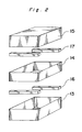
container 11 havingslits 12. - Fig. 3(a), (b) and (c) show schematical views of other embodiments of the container.
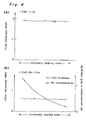
- Fig. 4 shows a graph of L-V (luminance - applied voltage) characteristics with respect to the above obtained EL device and another conventional EL device which was prepared by the electron beam deposition.
- Fig. 5(a) schematically shows an apparatus for chemical vapor deposition (CVD) and Fig. 5(b) schematically shows a substrate holder.
- Fig. 6(a) is a film thickness distribution in the uniformly heating area, Fig. 6(b) is a graph which indicates an Mn concentration and a ZnS:Mn film thickness distribution in the uniform by heating area.
- In the example illustrated in Fig. 1, a source material (ZnS) was heated to 900° to 1,000°C in a source furnace 9 and the resultant vapor was introduced through a
supply tube 1 into a reaction chamber 4 together with a carrier gas (H₂). A different carrier gas, for example He gas, could be used. Mn metal was heated to about 800° to 900°C in asource furnace 10, to which HCl gas was introduced and reacted as follows;
- The resulting MnCl₂ gas was introduced through a
supply tube 2 into the reaction chamber 4. The introduction of the source material gas could be done by direct introduction of ZnCl₂ gas, H₂S gas, MnCl₂ gas and the like. - A
substrate 8 was a glass substrate (14 cm x 17 cm) on which a transparent electrode of ITO was formed to about 1,500 angstrom thickness, and thereon a SiO₂ film and Si₃N₄ film were formed to a total of about 2,500 angstrom thickness. Twentysuch substrates 8 were placed in acontainer box 11 havingslits 12, of which an enlarged and schematical view is shown in Fig. 2. Thecontainer box 11 had base dimensions of 10 cm x 10 cm and a height of 20.6 cm. It was prepared by placing asquare tube 14 having a height of 5 cm on alower box 13 having a height of 7.5 cm withintermediate spacers 16 of 4 mm height, followed by placing anupper box 15 of 7.5 cm height thereon with intermediate 2mm spacers 17. Thecontainer box 11 thus had slit-like apertures formed by thespacers first area 18 was formed outside thecontainer box 11 andsecond area 19 was formed inside it. - The
container box 11 was placed on asubstrate holder 7 and thesubstrates 8 therein were heated by asubstrate furnace 5 to a temperature of 450° to 600°C. The pressure inside the reaction tube 4 was kept at about 10⁻² torr. Deposition was conducted at a substrate temperature of about 550°C for 60 minutes. - The physical properties of the deposited ZnS:Mn film were evaluated and the results are shown in Table 1. For a comparison, the same deposition was conducted without the
container 11 and the same evaluations were carried out. The results also are shown on Table 1.
- The measurement was conducted at 6 points on the luminescent layer (10 cm x 13 cm). As can be seen from Table 1, growth rate was reduced about 5%, but film thickness and Mn concentration distribution were improved. In particular, Mn concentration distribution was significantly improved. Since an optimum Mn concentration of a ZnS:Mn device lies generally within the range of 0.3 to 0.5 atomic %, the film obtained by the above example of the present invention was in this optimum range and no difference in regard with the physical properties of the ZnS:Mn film was observed between the substrates.
- Si₃N₄ film and Al₂O₃ film (both total about 1,500 angstrom) and Al film (about 3,000 angstrom) were deposited on ZnS:Mn film in this order to obtain an electroluminescent (EL) device. L-V (luminance-applied voltage) characteristics were measured for the above obtained EL device and for a conventional EL device which was prepared by electron beam deposition, and Fig. 4 shows the results. Although the thickness of the luminescent film and an MN concentration were common, the EL device prepared in accordance with the present invention emitted at lower voltage and had a higher saturated luminescence (see line A of Fig. 4) than the conventional EL device (see line B of Fig. 4). The reason seems to be that the ZnS:Mn film prepared by the electron beam deposition method has a region of low efficiency from the substrate to 3,000 angstrom, but in the film produced in accordance with the present invention such a region of low efficiency is less than 1,000 angstrom thick according to the observation of SEM. This difference of the film structure provides a high luminance at low voltage and high saturated luminescence.
- The above description relates to one example, but the shape and size of the
container 11 can be varied according to the shape and size of thesubstrate 8 and film-forming conditions. In the above example, the apertures are slits, but holes 20 can be used instead. The slits may be formed in the upper and lower surfaces of the container. Fig. 3(a), (b) and (c) show schematical views of the above described apertures. The invention, however, is not limited to these forms of apertures. The form and arrangement of apertures may be determined such that the source material gas is constantly fed. In the above example, a ZnS:Mn film was produced, but other films, such as ZnS:Tb, CaS:Eu and SrSl:Ce can be produced by the above method. - Using the process according to the present invention, a thin film EL device having a large area can be produced on an industrial scale. Also the process of the present invention has highly efficient utilization of the source material gas and lowers production costs.
- The invention being thus described, it will be obvious that the same may be varied in many ways. Such variations are not to be regarded as a departure from the scope of the invention.
- There are described above novel features which the skilled man will appreciate give rise to advantages. These are each independent aspects of the invention to be covered by the present application, irrespective of whether or not they are included within the scope of the following claims.
Claims (11)
- A process for preparing a thin film electroluminescent device comprising forming a luminescent layer on a substrate (8) by a reduced-pressure chemical vapor deposition method wherein a source material gas is introduced into a reaction chamber (4); an improvement being present in that;
said reaction chamber (4) includes a screening means (11) which screens said source material gas flow in said chamber to form a first area (18) in which said gas is flowing and a second area (19) in which said gas substantially does not flow,
said screening means (11) has apertures (12; 20) for connecting said first area (18) and said second area (19),
said substrate (8) is placed in said second area (19), to which the source material is supplied by means of gas diffusion. - A process according to claim 1 wherein said source material and carrier gas comprise;
ZnS and H₂ (or He, Ar) gas, and
Mn and HCl gas. - A process according to claim 1 wherein said source material gas comprises;
ZnCl₂ gas and H₂S gas, and
MnCl₂ gas. - A process according to claim 1 wherein said screening means is a container box formed by placing a square tube (14) on a lower box (13) through a spacer means (16), followed by placing an upper box (15) thereon through a further spacer means (17).
- A process according to claim 1 wherein said luminescent layer is ZnS:Mn, ZnS:Tb, CaS:Eu or SeS:Ce.
- Apparatus for performing a reduced-pressure CVD process for the deposition of a material layer on a substrate (8), said apparatus including a reaction chamber (4) and means (1, 2) for introducing into said reaction chamber a source material gas which in use flows through said reaction chamber, characterised by means (11) defining within said chamber a zone (19) in which, in use, the substrate (8) is accommodated and substantially no gas flow exists, said zone-defining means (11) including aperture means (12, 20) through which the source material gas diffuses.
- Apparatus according to claim 6, further characterised in that said aperture means (12, 20) is adapted to provide substantially uniform concentration of diffused material gas in said zone (19) in the direction of material gas flow in said reaction chamber (4).
- Apparatus according to claim 7 wherein the aperture means provides an opening area for gas diffusion, which area is greater downstream than upstream, relative to the direction of material gas flow.
- Apparatus according to claim 8 wherein the aperture means comprises different width slits extending across said direction of flow.
- Apparatus according to claim 8 wherein the aperture means comprises holes.
- A thin film electroluminescent device produced by a process according to any of claims 1 to 5.
Applications Claiming Priority (2)
| Application Number | Priority Date | Filing Date | Title |
|---|---|---|---|
| JP3190/90 | 1990-01-09 | ||
| JP2003190A JPH0793191B2 (en) | 1990-01-09 | 1990-01-09 | Method of manufacturing thin film EL device |
Publications (2)
| Publication Number | Publication Date |
|---|---|
| EP0437355A1 true EP0437355A1 (en) | 1991-07-17 |
| EP0437355B1 EP0437355B1 (en) | 1996-06-05 |
Family
ID=11550487
Family Applications (1)
| Application Number | Title | Priority Date | Filing Date |
|---|---|---|---|
| EP91300159A Expired - Lifetime EP0437355B1 (en) | 1990-01-09 | 1991-01-09 | Process and apparatus for preparing a thin film electroluminescent device |
Country Status (5)
| Country | Link |
|---|---|
| US (1) | US5147683A (en) |
| EP (1) | EP0437355B1 (en) |
| JP (1) | JPH0793191B2 (en) |
| DE (1) | DE69119916T2 (en) |
| FI (1) | FI101585B1 (en) |
Cited By (2)
| Publication number | Priority date | Publication date | Assignee | Title |
|---|---|---|---|---|
| EP1517340A2 (en) * | 2003-09-17 | 2005-03-23 | Konica Minolta Medical & Graphic, Inc. | Radiographic image conversion panel and production method thereof |
| CN103289693A (en) * | 2012-02-28 | 2013-09-11 | 海洋王照明科技股份有限公司 | Cerium-terbium-codoped borophosphate luminescent material, preparation method and application of same |
Families Citing this family (5)
| Publication number | Priority date | Publication date | Assignee | Title |
|---|---|---|---|---|
| US5300316A (en) * | 1991-12-11 | 1994-04-05 | Kabushiki Kaisha Komatsu Seisakusho | Method of forming thin oxysulfide film |
| US6689422B1 (en) * | 1994-02-16 | 2004-02-10 | Howmet Research Corporation | CVD codeposition of A1 and one or more reactive (gettering) elements to form protective aluminide coating |
| JP3564737B2 (en) * | 1994-06-24 | 2004-09-15 | 株式会社デンソー | Manufacturing method and manufacturing apparatus for electroluminescent element |
| US5989733A (en) | 1996-07-23 | 1999-11-23 | Howmet Research Corporation | Active element modified platinum aluminide diffusion coating and CVD coating method |
| CN107604340B (en) * | 2017-08-31 | 2023-09-01 | 安徽光智科技有限公司 | Chemical Vapor Deposition Furnace |
Citations (3)
| Publication number | Priority date | Publication date | Assignee | Title |
|---|---|---|---|---|
| US4548159A (en) * | 1984-07-06 | 1985-10-22 | Anicon, Inc. | Chemical vapor deposition wafer boat |
| US4582720A (en) * | 1982-09-20 | 1986-04-15 | Semiconductor Energy Laboratory Co., Ltd. | Method and apparatus for forming non-single-crystal layer |
| EP0342063A2 (en) * | 1988-05-13 | 1989-11-15 | Sharp Kabushiki Kaisha | Process for preparing an electroluminescent film |
-
1990
- 1990-01-09 JP JP2003190A patent/JPH0793191B2/en not_active Expired - Lifetime
-
1991
- 1991-01-08 FI FI910095A patent/FI101585B1/en active
- 1991-01-08 US US07/638,841 patent/US5147683A/en not_active Expired - Lifetime
- 1991-01-09 EP EP91300159A patent/EP0437355B1/en not_active Expired - Lifetime
- 1991-01-09 DE DE69119916T patent/DE69119916T2/en not_active Expired - Fee Related
Patent Citations (3)
| Publication number | Priority date | Publication date | Assignee | Title |
|---|---|---|---|---|
| US4582720A (en) * | 1982-09-20 | 1986-04-15 | Semiconductor Energy Laboratory Co., Ltd. | Method and apparatus for forming non-single-crystal layer |
| US4548159A (en) * | 1984-07-06 | 1985-10-22 | Anicon, Inc. | Chemical vapor deposition wafer boat |
| EP0342063A2 (en) * | 1988-05-13 | 1989-11-15 | Sharp Kabushiki Kaisha | Process for preparing an electroluminescent film |
Cited By (9)
| Publication number | Priority date | Publication date | Assignee | Title |
|---|---|---|---|---|
| EP1517340A2 (en) * | 2003-09-17 | 2005-03-23 | Konica Minolta Medical & Graphic, Inc. | Radiographic image conversion panel and production method thereof |
| EP1517340A3 (en) * | 2003-09-17 | 2005-06-01 | Konica Minolta Medical & Graphic, Inc. | Radiographic image conversion panel and production method thereof |
| US7282310B2 (en) | 2003-09-17 | 2007-10-16 | Konica Minolta Medical & Graphic, Inc. | Radiographic image conversion panel and production method thereof |
| EP2001027A2 (en) | 2003-09-17 | 2008-12-10 | Konica Minolta Medical & Graphic, Inc. | Radiographic image conversion panel and production method thereof |
| US7704651B2 (en) | 2003-09-17 | 2010-04-27 | Konica Minolta Medical & Graphic, Inc. | Radiographic image conversion panel and production method thereof |
| EP2001027A3 (en) * | 2003-09-17 | 2011-09-21 | Konica Minolta Medical & Graphic, Inc. | Radiographic image conversion panel and production method thereof |
| EP2405448A3 (en) * | 2003-09-17 | 2012-07-18 | Konica Minolta Medical & Graphic, Inc. | Radiographic image conversion panel and production method thereof |
| EP2405447A3 (en) * | 2003-09-17 | 2012-07-18 | Konica Minolta Medical & Graphic, Inc. | Radiographic image conversion panel and production method thereof |
| CN103289693A (en) * | 2012-02-28 | 2013-09-11 | 海洋王照明科技股份有限公司 | Cerium-terbium-codoped borophosphate luminescent material, preparation method and application of same |
Also Published As
| Publication number | Publication date |
|---|---|
| FI910095A0 (en) | 1991-01-08 |
| JPH03208298A (en) | 1991-09-11 |
| US5147683A (en) | 1992-09-15 |
| JPH0793191B2 (en) | 1995-10-09 |
| FI101585B (en) | 1998-07-15 |
| DE69119916D1 (en) | 1996-07-11 |
| FI910095A (en) | 1991-07-10 |
| FI101585B1 (en) | 1998-07-15 |
| EP0437355B1 (en) | 1996-06-05 |
| DE69119916T2 (en) | 1996-11-28 |
Similar Documents
| Publication | Publication Date | Title |
|---|---|---|
| US5294286A (en) | Process for forming a thin film of silicon | |
| US6297522B1 (en) | Highly uniform silicon carbide epitaxial layers | |
| US5334250A (en) | Vapor deposition apparatus for using solid starting materials | |
| EP0548944A1 (en) | Chemical vapor deposition method and apparatus making use of liquid starting material | |
| EP0605205A1 (en) | Chemical vapor deposition apparatus | |
| US5356657A (en) | Method of manufacturing an electroluminescent device | |
| US4735822A (en) | Method for producing an electronic device having a multi-layer structure | |
| US5593497A (en) | Method for forming a deposited film | |
| EP0437355A1 (en) | Process and apparatus for preparing a thin film electroluminescent device | |
| US5390626A (en) | Process for formation of silicon carbide film | |
| US6004885A (en) | Thin film formation on semiconductor wafer | |
| US5750188A (en) | Method for forming a thin film of a non-stoichiometric metal oxide | |
| US5185181A (en) | Process for preparing an electroluminescent thin film | |
| JPH0421780A (en) | Vapor growth device | |
| US5439844A (en) | Process for forming deposited film | |
| US5624719A (en) | Process for synthesizing diamond in a vapor phase | |
| US4822636A (en) | Method for forming deposited film | |
| US5275840A (en) | Manufacturing method for electroluminescent thin film | |
| EP0342063A2 (en) | Process for preparing an electroluminescent film | |
| US5372839A (en) | Process for preparing an electroluminescent film | |
| US3565704A (en) | Aluminum nitride films and processes for producing the same | |
| JPH02152191A (en) | Vapor deposition method of electroluminescent luminous membrane | |
| JP2726353B2 (en) | Method for growing electroluminescent thin film | |
| Murota et al. | Control of germanium atomic layer formation on silicon using flash heating in germanium CVD | |
| JPH01766A (en) | semiconductor equipment |
Legal Events
| Date | Code | Title | Description |
|---|---|---|---|
| PUAI | Public reference made under article 153(3) epc to a published international application that has entered the european phase |
Free format text: ORIGINAL CODE: 0009012 |
|
| AK | Designated contracting states |
Kind code of ref document: A1 Designated state(s): DE FR GB |
|
| 17P | Request for examination filed |
Effective date: 19910801 |
|
| 17Q | First examination report despatched |
Effective date: 19940214 |
|
| GRAA | (expected) grant |
Free format text: ORIGINAL CODE: 0009210 |
|
| AK | Designated contracting states |
Kind code of ref document: B1 Designated state(s): DE FR GB |
|
| REF | Corresponds to: |
Ref document number: 69119916 Country of ref document: DE Date of ref document: 19960711 |
|
| ET | Fr: translation filed | ||
| GRAH | Despatch of communication of intention to grant a patent |
Free format text: ORIGINAL CODE: EPIDOS IGRA |
|
| PLBE | No opposition filed within time limit |
Free format text: ORIGINAL CODE: 0009261 |
|
| STAA | Information on the status of an ep patent application or granted ep patent |
Free format text: STATUS: NO OPPOSITION FILED WITHIN TIME LIMIT |
|
| 26N | No opposition filed | ||
| PGFP | Annual fee paid to national office [announced via postgrant information from national office to epo] |
Ref country code: DE Payment date: 20010102 Year of fee payment: 11 |
|
| PGFP | Annual fee paid to national office [announced via postgrant information from national office to epo] |
Ref country code: GB Payment date: 20010103 Year of fee payment: 11 |
|
| PGFP | Annual fee paid to national office [announced via postgrant information from national office to epo] |
Ref country code: FR Payment date: 20010125 Year of fee payment: 11 |
|
| REG | Reference to a national code |
Ref country code: GB Ref legal event code: IF02 |
|
| PG25 | Lapsed in a contracting state [announced via postgrant information from national office to epo] |
Ref country code: GB Free format text: LAPSE BECAUSE OF NON-PAYMENT OF DUE FEES Effective date: 20020109 |
|
| PG25 | Lapsed in a contracting state [announced via postgrant information from national office to epo] |
Ref country code: DE Free format text: LAPSE BECAUSE OF NON-PAYMENT OF DUE FEES Effective date: 20020801 |
|
| GBPC | Gb: european patent ceased through non-payment of renewal fee |
Effective date: 20020109 |
|
| PG25 | Lapsed in a contracting state [announced via postgrant information from national office to epo] |
Ref country code: FR Free format text: LAPSE BECAUSE OF NON-PAYMENT OF DUE FEES Effective date: 20020930 |
|
| REG | Reference to a national code |
Ref country code: FR Ref legal event code: ST |