EP0430500A2 - System and method for atomic access to an input/output device with direct memory access - Google Patents
System and method for atomic access to an input/output device with direct memory access Download PDFInfo
- Publication number
- EP0430500A2 EP0430500A2 EP90312471A EP90312471A EP0430500A2 EP 0430500 A2 EP0430500 A2 EP 0430500A2 EP 90312471 A EP90312471 A EP 90312471A EP 90312471 A EP90312471 A EP 90312471A EP 0430500 A2 EP0430500 A2 EP 0430500A2
- Authority
- EP
- European Patent Office
- Prior art keywords
- input
- output device
- command packet
- processor
- graphics
- Prior art date
- Legal status (The legal status is an assumption and is not a legal conclusion. Google has not performed a legal analysis and makes no representation as to the accuracy of the status listed.)
- Granted
Links
Images

Classifications
-
- G—PHYSICS
- G06—COMPUTING; CALCULATING OR COUNTING
- G06F—ELECTRIC DIGITAL DATA PROCESSING
- G06F15/00—Digital computers in general; Data processing equipment in general
- G06F15/16—Combinations of two or more digital computers each having at least an arithmetic unit, a program unit and a register, e.g. for a simultaneous processing of several programs
- G06F15/163—Interprocessor communication
- G06F15/167—Interprocessor communication using a common memory, e.g. mailbox
-
- G—PHYSICS
- G06—COMPUTING; CALCULATING OR COUNTING
- G06F—ELECTRIC DIGITAL DATA PROCESSING
- G06F3/00—Input arrangements for transferring data to be processed into a form capable of being handled by the computer; Output arrangements for transferring data from processing unit to output unit, e.g. interface arrangements
- G06F3/14—Digital output to display device ; Cooperation and interconnection of the display device with other functional units
Definitions
- the present invention relates generally to a system and method for data transfer to a direct memory access (DMA) input/output (I/O) device which allows a client to access atomically the I/O device.
- DMA direct memory access
- I/O input/output
- Accessing atomically means that an instruction consisting of more than one individual operation is carried out completely, without interruption for any other operation. More particularly, it relates to such a system and method in a multiprocessor system where multiple processors concurrently access a single I/O device.
- An I/O device typically receives data and instructions from the system's main computing resources in one of two ways: either through direct memory-mapped access of I/O registers, or through a DMA mechanism by which the I/O device transfers data directly to and from the main memory subsystem. In either scheme, if the size of the data transfer is larger than an atomic access on the system bus, there are multiple concurrent clients of the I/O device, and the I/O device has a single input stream, there must be a mechanism to synchronize the I/O device among the several clients.
- Some processor instruction sets contain interlocked instructions, which allow a processor of an I/O device client to perform multiple logical instructions as a single atomic instruction. For example, a processor may test a bit in memory, branch if it is clear, and then set the bit, all within a single instruction. This allows mutual exclusion on shared resources to be implemented through software locks. The I/O device or other shared resource is considered “locked” or unavailable if the bit is set. The process that set the bit "owns" the resource. Systems without interlocked instructions must go through some other atomic protocol, perhaps synchronizing through the operating system or some other unique process.
- graphic subsystems in a multiclient, multiprocessor environment have states maintained internally that are set up in a previous operation and stay for a subsequent operation by the same processor. With interruption by another processor, there is no assurance that those states have been maintained. A technique for executing atomic instructions in this environment is therefore required.
- a system for atomic access to an I/O device with direct memory access has at least one host data processor.
- a memory is connected to the at least one host data processor by a bus.
- a graphics subsystem comprising the input/output device is connected to the bus.
- the memory has a locked-down buffer for storing a command packet including a plurality of instructions for the graphics subsystem.
- the at least one host data processor includes a first program for generating the command packet.
- the graphics subsystem includes a graphics processor addressable by the at least one host data processor under control of the first program to determine availability of the graphics processor.
- the graphics processor includes a second program for initiating transfer of the command packet to the graphics subsystem as an input/output read transaction when the graphics processor is available. The second program executes the plurality of instructions atomically.
- a method for atomic access to an I/O device with direct memory access includes generating a command packet including a plurality of instructions for the input/output device.
- the command packet is stored in a memory having a physically contiguous locked-down memory buffer.
- the input/output device is interrogated to determine availability of the input/output device.
- a transfer of the command packet to the input/output device as an input/output read transaction is initiated when the input/output device is available.
- the plurality of instructions is executed atomically.
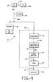
- a CPU 32 is connected to a floating point processor (FPU) 34 by bus 36.
- the CPU 32 is connected by a 32-bit system bus 38 to a random access memory (RAM) 40, a cache 42 and an interface 44 in graphics subsystem 45.
- the interface 44 is connected by bus 46 to graphics processor 48.
- the graphics processor 48 is connected by 120-bit graphics bus 50 to frame buffer 52.
- the frame buffer 52 are connected to a video digital to analog converter (DAC) 54 by bus 56.
- the DAC 54 is connected to video display 58 by line 60.
- the graphics subsystem 45 is an I/O device, and atomic access to it is required.
- Command packet interface 44 to the graphics subsystem 45 transfers geometry and graphics context information from main memory 40 to the graphics subsystem 45. For such transfers, an application writes a list of commands to a physically contiguous locked-down memory buffer 47 in its own address space. Since the system 30 has DMA, the buffer 47 resides in the main memory system 40. The system 30 has a write-back cache 42, so it moves the contents of the buffer 47 into cache 42, generating little or no traffic on bus 38 when writing to the buffer. On systems with no DMA, this buffer will reside locally on the graphics subsystem.
- the CPU 32 tells the graphics subsystem 45, via a read from an I/O address on the graphics subsystem 45, that it should begin a transfer of the command packet. Status of the operation is returned as a result of the I/O read transaction.
- the graphics subsystem 45 parses the packet and executes the appropriate operations, finding the details of the transaction syntax encoded in the first longword of the command packet. Execution of the commands in the packet is atomic, implying that all commands in one packet are executed before any commands in the next packet. Furthermore, the execution order is guaranteed to be the order in which the commands appear in the packet.
- Table 1 below shows the outline of a procedure that issues a command to draw a line in the frame buffer 52.
- the global variable, pPacket is the virtual addresses of a physically contiguous locked-down memory buffer serving as the graphics subsystem 45 command buffer 47. To avoid synchronization problems concerning the command packet memory, two command packet buffers 47 are used alternately. The alternation of command packets is handled by the switchPacket() routine.
- the Line procedure must first fill in the command packet with header information and vertex data. It then does a read from the I/O address, stamp , and receives status over the system bus 38. Table II enumerates the status values that can be returned by the graphics subsystem 45 as a result of the I/O read. Table II Value Status Description 0 GOOD Data was accepted 1 BUSY Subsystem 45 is unavailable; retry later As rectangular clipping is done in hardware, the line is clipped successively to each clipping rectangle in the window's clip list. The clip rectangle is placed in the command packet by the fillLinePacket() routine.
- the Line procedure checks the status of the I/O read transaction. If the status is GOOD, then the graphics subsystem 45 immediately initiates the transfer of the command packet. A BUSY status causes a software retry, since the procedure just spins on the status word. Neither the code of Table I nor the procedural interface of Table II is appropriate for high performance graphics. They are shown to give a trivial example of the framework of the command packet interface.
- the command packet interface provides atomic access for high level commands, such as drawing lines and triangles. Access to the graphics subsystem 45 is gained through the framework described above. In order to guarantee an atomic operation containing both the I/O read transaction issued by the application and the command packet transactions issued by the graphics subsystem 45, the physical address of the command packet is encoded in the address of the I/O read transaction. This encoding provides the packet address to the graphics subsystem 45 so that it can carry out the command packet transfer, while the application receives status as part of the same atomic operation.
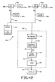
- Figure 2 shows a multiprocessor form of a system 30a, in which a first CPU 32a is connected to a FPU 34a by bus 36a.
- a cache 42a is connected to the CPU 32a by bus 38a.
- a second CPU 32b is connected to a FPU 34b by bus 36b.
- a cache 42b is connected to the CPU 32b by bus 38a.
- the construction and operation of the Figure 2 embodiment of the invention is the same as in the Figure 1 embodiment.
- bits 21:2 of the I/O read transaction address 70 contain bits 30:11 of the command packet address 72.
- the positions specified are for a 32-bit system bus 38. If the available physical address space is less than 32 bits, then the high order bits are ignored.
- the remaining bits of the address of the I/O read transaction contain an implementation specific base address that is decoded by the graphics subsystem 45, indicating that a packet transfer should be initiated.
- the address of the command packet is created as follows: bits 10:0 of the command packet address 72 are zero, forcing the packet to be aligned on a 2048 byte boundary; bits 30:11 equal bits 21:2 of the I/O read transaction address 70; bit 31 of the command packet address is zero.
- Figure 2 shows the mapping from the address 70 of the I/O read transaction to the base address 72 of the command packet transfer.
Abstract
Description
- The present invention relates generally to a system and method for data transfer to a direct memory access (DMA) input/output (I/O) device which allows a client to access atomically the I/O device. Accessing atomically means that an instruction consisting of more than one individual operation is carried out completely, without interruption for any other operation. More particularly, it relates to such a system and method in a multiprocessor system where multiple processors concurrently access a single I/O device.
- An I/O device typically receives data and instructions from the system's main computing resources in one of two ways: either through direct memory-mapped access of I/O registers, or through a DMA mechanism by which the I/O device transfers data directly to and from the main memory subsystem. In either scheme, if the size of the data transfer is larger than an atomic access on the system bus, there are multiple concurrent clients of the I/O device, and the I/O device has a single input stream, there must be a mechanism to synchronize the I/O device among the several clients.
- Mutual exclusion of I/O devices, or other shared resources, is typically achieved through software interlocks. Some processor instruction sets contain interlocked instructions, which allow a processor of an I/O device client to perform multiple logical instructions as a single atomic instruction. For example, a processor may test a bit in memory, branch if it is clear, and then set the bit, all within a single instruction. This allows mutual exclusion on shared resources to be implemented through software locks. The I/O device or other shared resource is considered "locked" or unavailable if the bit is set. The process that set the bit "owns" the resource. Systems without interlocked instructions must go through some other atomic protocol, perhaps synchronizing through the operating system or some other unique process.
- In particular, graphic subsystems in a multiclient, multiprocessor environment have states maintained internally that are set up in a previous operation and stay for a subsequent operation by the same processor. With interruption by another processor, there is no assurance that those states have been maintained. A technique for executing atomic instructions in this environment is therefore required.
- A system for atomic access to an I/O device with direct memory access in accordance with this invention has at least one host data processor. A memory is connected to the at least one host data processor by a bus. A graphics subsystem comprising the input/output device is connected to the bus. The memory has a locked-down buffer for storing a command packet including a plurality of instructions for the graphics subsystem. The at least one host data processor includes a first program for generating the command packet. The graphics subsystem includes a graphics processor addressable by the at least one host data processor under control of the first program to determine availability of the graphics processor. The graphics processor includes a second program for initiating transfer of the command packet to the graphics subsystem as an input/output read transaction when the graphics processor is available. The second program executes the plurality of instructions atomically.
- A method for atomic access to an I/O device with direct memory access in accordance with this invention includes generating a command packet including a plurality of instructions for the input/output device. The command packet is stored in a memory having a physically contiguous locked-down memory buffer. The input/output device is interrogated to determine availability of the input/output device. A transfer of the command packet to the input/output device as an input/output read transaction is initiated when the input/output device is available. The plurality of instructions is executed atomically.
- The attainment of the foregoing and related objects, advantages and features of the invention should be more readily apparent to those skilled in the art, after review of the following more detailed description of the invention, taken together with the drawings, in which:
-
- Figure 1 is a block diagram of a system in accordance with the invention.
- Figure 2 is a block diagram of another embodiment of a system in accordance with the invention.
- Figure 3 is a diagram showing mapping from an address of an I/O read transaction to a base address of a command packet transfer in practice of the invention.
-
- Turning now to the drawings, more particularly to Figure 1, a block diagram of a
system 30 for atomic access to an I/O device with DMA is shown. ACPU 32 is connected to a floating point processor (FPU) 34 bybus 36. TheCPU 32 is connected by a 32-bit system bus 38 to a random access memory (RAM) 40, acache 42 and aninterface 44 ingraphics subsystem 45. Theinterface 44 is connected by bus 46 tographics processor 48. Thegraphics processor 48 is connected by 120-bit graphics bus 50 toframe buffer 52. Theframe buffer 52 are connected to a video digital to analog converter (DAC) 54 bybus 56. The DAC 54 is connected tovideo display 58 byline 60. In this system, thegraphics subsystem 45 is an I/O device, and atomic access to it is required. -
Command packet interface 44 to thegraphics subsystem 45 transfers geometry and graphics context information frommain memory 40 to thegraphics subsystem 45. For such transfers, an application writes a list of commands to a physically contiguous locked-downmemory buffer 47 in its own address space. Since thesystem 30 has DMA, thebuffer 47 resides in themain memory system 40. Thesystem 30 has a write-back cache 42, so it moves the contents of thebuffer 47 intocache 42, generating little or no traffic onbus 38 when writing to the buffer. On systems with no DMA, this buffer will reside locally on the graphics subsystem. - When the
buffer 47 is full, theCPU 32 tells thegraphics subsystem 45, via a read from an I/O address on thegraphics subsystem 45, that it should begin a transfer of the command packet. Status of the operation is returned as a result of the I/O read transaction. - After initiating the command packet transfer, the
graphics subsystem 45 parses the packet and executes the appropriate operations, finding the details of the transaction syntax encoded in the first longword of the command packet. Execution of the commands in the packet is atomic, implying that all commands in one packet are executed before any commands in the next packet. Furthermore, the execution order is guaranteed to be the order in which the commands appear in the packet. - The following discussion describes the general framework of application software using the
command packet interface 44. A discussion of the command protocol follows. - Table 1 below shows the outline of a procedure that issues a command to draw a line in the
frame buffer 52.The global variable, pPacket, is the virtual addresses of a physically contiguous locked-down memory buffer serving as the
graphics subsystem 45command buffer 47. To avoid synchronization problems concerning the command packet memory, twocommand packet buffers 47 are used alternately. The alternation of command packets is handled by the switchPacket() routine. - The Line procedure must first fill in the command packet with header information and vertex data. It then does a read from the I/O address, stamp, and receives status over the
system bus 38. Table II enumerates the status values that can be returned by thegraphics subsystem 45 as a result of the I/O read.Table II Value Status Description 0 GOOD Data was accepted 1 BUSY Subsystem 45 is unavailable; retry later - The Line procedure checks the status of the I/O read transaction. If the status is GOOD, then the
graphics subsystem 45 immediately initiates the transfer of the command packet. A BUSY status causes a software retry, since the procedure just spins on the status word. Neither the code of Table I nor the procedural interface of Table II is appropriate for high performance graphics. They are shown to give a trivial example of the framework of the command packet interface. - The command packet interface provides atomic access for high level commands, such as drawing lines and triangles. Access to the
graphics subsystem 45 is gained through the framework described above. In order to guarantee an atomic operation containing both the I/O read transaction issued by the application and the command packet transactions issued by thegraphics subsystem 45, the physical address of the command packet is encoded in the address of the I/O read transaction. This encoding provides the packet address to thegraphics subsystem 45 so that it can carry out the command packet transfer, while the application receives status as part of the same atomic operation. - Figure 2 shows a multiprocessor form of a
system 30a, in which afirst CPU 32a is connected to aFPU 34a bybus 36a. Acache 42a is connected to theCPU 32a bybus 38a. Asecond CPU 32b is connected to aFPU 34b bybus 36b. Acache 42b is connected to theCPU 32b bybus 38a. Other than this construction and the fact that thesystem 30a operates in a multiprocessor mode, the construction and operation of the Figure 2 embodiment of the invention is the same as in the Figure 1 embodiment. - As shown in Figure 3, bits 21:2 of the I/O read
transaction address 70 contain bits 30:11 of thecommand packet address 72. In practice, the exact bit positions are dependent on the system bus employed. The positions specified are for a 32-bit system bus 38. If the available physical address space is less than 32 bits, then the high order bits are ignored. The remaining bits of the address of the I/O read transaction contain an implementation specific base address that is decoded by thegraphics subsystem 45, indicating that a packet transfer should be initiated. The address of the command packet is created as follows: bits 10:0 of thecommand packet address 72 are zero, forcing the packet to be aligned on a 2048 byte boundary; bits 30:11 equal bits 21:2 of the I/O readtransaction address 70;bit 31 of the command packet address is zero. Figure 2 shows the mapping from theaddress 70 of the I/O read transaction to thebase address 72 of the command packet transfer. - It should further be apparent to those skilled in the art that various changes in form and details of the invention as shown and described may be made. It is intended that such changes be included within the spirit and scope of the claims appended hereto.
Claims (15)
Applications Claiming Priority (2)
| Application Number | Priority Date | Filing Date | Title |
|---|---|---|---|
| US07/440,588 US5218678A (en) | 1989-11-17 | 1989-11-17 | System and method for atomic access to an input/output device with direct memory access |
| US440588 | 1989-11-17 |
Publications (3)
| Publication Number | Publication Date |
|---|---|
| EP0430500A2 true EP0430500A2 (en) | 1991-06-05 |
| EP0430500A3 EP0430500A3 (en) | 1992-03-04 |
| EP0430500B1 EP0430500B1 (en) | 1996-09-11 |
Family
ID=23749363
Family Applications (1)
| Application Number | Title | Priority Date | Filing Date |
|---|---|---|---|
| EP90312471A Expired - Lifetime EP0430500B1 (en) | 1989-11-17 | 1990-11-15 | System and method for atomic access to an input/output device with direct memory access |
Country Status (5)
| Country | Link |
|---|---|
| US (1) | US5218678A (en) |
| EP (1) | EP0430500B1 (en) |
| JP (1) | JPH03212753A (en) |
| CA (1) | CA2030021A1 (en) |
| DE (1) | DE69028492T2 (en) |
Cited By (2)
| Publication number | Priority date | Publication date | Assignee | Title |
|---|---|---|---|---|
| WO2000010128A1 (en) * | 1998-08-10 | 2000-02-24 | Diamond Multimedia Systems, Inc. | Graphic request management system |
| SG81184A1 (en) * | 1993-12-20 | 2001-06-19 | At & T Corp | Application-oriented telecommunication system interface |
Families Citing this family (6)
| Publication number | Priority date | Publication date | Assignee | Title |
|---|---|---|---|---|
| US5666509A (en) * | 1994-03-24 | 1997-09-09 | Motorola, Inc. | Data processing system for performing either a precise memory access or an imprecise memory access based upon a logical address value and method thereof |
| US5835742A (en) * | 1994-06-14 | 1998-11-10 | Apple Computer, Inc. | System and method for executing indivisible memory operations in multiple processor computer systems with multiple busses |
| US5548780A (en) * | 1994-07-21 | 1996-08-20 | Apple Computer, Inc. | Method for semaphore communication between incompatible bus locking architectures |
| US6128674A (en) * | 1997-08-08 | 2000-10-03 | International Business Machines Corporation | Method of minimizing host CPU utilization in driving an adapter by residing in system memory a command/status block a soft interrupt block and a status block queue |
| US6430628B1 (en) * | 1998-12-08 | 2002-08-06 | Intel Corporation | Method and apparatus for reducing direct memory access transfers using smart coalescing |
| US7752340B1 (en) * | 2006-03-31 | 2010-07-06 | Emc Corporation | Atomic command retry in a data storage system |
Citations (3)
| Publication number | Priority date | Publication date | Assignee | Title |
|---|---|---|---|---|
| US4402046A (en) * | 1978-12-21 | 1983-08-30 | Intel Corporation | Interprocessor communication system |
| EP0330425A2 (en) * | 1988-02-23 | 1989-08-30 | Digital Equipment Corporation | Symmetric multi-processing control arrangement |
| EP0381325A2 (en) * | 1989-02-03 | 1990-08-08 | Digital Equipment Corporation | Synchronising and processing of memory access operations |
Family Cites Families (11)
| Publication number | Priority date | Publication date | Assignee | Title |
|---|---|---|---|---|
| US4491916A (en) * | 1979-11-05 | 1985-01-01 | Litton Resources Systems, Inc. | Large volume, high speed data processor |
| US4449182A (en) * | 1981-10-05 | 1984-05-15 | Digital Equipment Corporation | Interface between a pair of processors, such as host and peripheral-controlling processors in data processing systems |
| US4777595A (en) * | 1982-05-07 | 1988-10-11 | Digital Equipment Corporation | Apparatus for transferring blocks of information from one node to a second node in a computer network |
| US4689739A (en) * | 1983-03-28 | 1987-08-25 | Xerox Corporation | Method for providing priority interrupts in an electrophotographic machine |
| US4814977A (en) * | 1983-10-18 | 1989-03-21 | S&C Electric Company | Apparatus and method for direct memory to peripheral and peripheral to memory data transfers |
| US4604694A (en) * | 1983-12-14 | 1986-08-05 | International Business Machines Corporation | Shared and exclusive access control |
| JPS61107456A (en) * | 1984-10-30 | 1986-05-26 | Toshiba Corp | Interrupt control system |
| US4719621A (en) * | 1985-07-15 | 1988-01-12 | Raytheon Company | Packet fastbus |
| US4847754A (en) * | 1985-10-15 | 1989-07-11 | International Business Machines Corporation | Extended atomic operations |
| US5014186A (en) * | 1986-08-01 | 1991-05-07 | International Business Machines Corporation | Data-processing system having a packet transfer type input/output system |
| US4953101A (en) * | 1987-11-24 | 1990-08-28 | Digital Equipment Corporation | Software configurable memory architecture for data processing system having graphics capability |
-
1989
- 1989-11-17 US US07/440,588 patent/US5218678A/en not_active Expired - Lifetime
-
1990
- 1990-11-15 EP EP90312471A patent/EP0430500B1/en not_active Expired - Lifetime
- 1990-11-15 CA CA002030021A patent/CA2030021A1/en not_active Abandoned
- 1990-11-15 DE DE69028492T patent/DE69028492T2/en not_active Expired - Lifetime
- 1990-11-16 JP JP2311224A patent/JPH03212753A/en active Pending
Patent Citations (3)
| Publication number | Priority date | Publication date | Assignee | Title |
|---|---|---|---|---|
| US4402046A (en) * | 1978-12-21 | 1983-08-30 | Intel Corporation | Interprocessor communication system |
| EP0330425A2 (en) * | 1988-02-23 | 1989-08-30 | Digital Equipment Corporation | Symmetric multi-processing control arrangement |
| EP0381325A2 (en) * | 1989-02-03 | 1990-08-08 | Digital Equipment Corporation | Synchronising and processing of memory access operations |
Cited By (2)
| Publication number | Priority date | Publication date | Assignee | Title |
|---|---|---|---|---|
| SG81184A1 (en) * | 1993-12-20 | 2001-06-19 | At & T Corp | Application-oriented telecommunication system interface |
| WO2000010128A1 (en) * | 1998-08-10 | 2000-02-24 | Diamond Multimedia Systems, Inc. | Graphic request management system |
Also Published As
| Publication number | Publication date |
|---|---|
| EP0430500B1 (en) | 1996-09-11 |
| DE69028492D1 (en) | 1996-10-17 |
| CA2030021A1 (en) | 1991-05-18 |
| DE69028492T2 (en) | 1997-04-03 |
| EP0430500A3 (en) | 1992-03-04 |
| US5218678A (en) | 1993-06-08 |
| JPH03212753A (en) | 1991-09-18 |
Similar Documents
| Publication | Publication Date | Title |
|---|---|---|
| US5224215A (en) | Message queue processing among cooperative processors having significant speed differences | |
| US5404522A (en) | System for constructing a partitioned queue of DMA data transfer requests for movements of data between a host processor and a digital signal processor | |
| US6023738A (en) | Method and apparatus for accelerating the transfer of graphical images | |
| US6046752A (en) | Peer-to-peer parallel processing graphics accelerator | |
| US6470380B1 (en) | Signal processing device accessible as memory | |
| JP3273202B2 (en) | Method of transferring data through a plurality of data channels and circuit architecture thereof | |
| US5781199A (en) | Parallel processing method for use with graphics processor | |
| US5805930A (en) | System for FIFO informing the availability of stages to store commands which include data and virtual address sent directly from application programs | |
| US5696990A (en) | Method and apparatus for providing improved flow control for input/output operations in a computer system having a FIFO circuit and an overflow storage area | |
| JPH04290150A (en) | Device and method for controlling bidirectional fifo as interface between two buses in multi-task system | |
| US5918050A (en) | Apparatus accessed at a physical I/O address for address and data translation and for context switching of I/O devices in response to commands from application programs | |
| CN100589089C (en) | Apparatus and method for handling DMA requests in a virtual memory environment | |
| US5638535A (en) | Method and apparatus for providing flow control with lying for input/output operations in a computer system | |
| JP2774862B2 (en) | DMA control device and information processing device | |
| US5396597A (en) | System for transferring data between processors via dual buffers within system memory with first and second processors accessing system memory directly and indirectly | |
| JPH07105126A (en) | System and method for interface | |
| US20020099881A1 (en) | Method and system for data transfer | |
| EP0430500B1 (en) | System and method for atomic access to an input/output device with direct memory access | |
| WO2000000887A9 (en) | Method and apparatus for transporting information to a graphic accelerator card | |
| US5764861A (en) | Apparatus and method for controlling context of input/output devices in a computer system | |
| US5129065A (en) | Apparatus and methods for interface register handshake for controlling devices | |
| US5685011A (en) | Apparatus for handling failures to provide a safe address translation in an improved input/output architecture for a computer system | |
| US6201547B1 (en) | Method and apparatus for sequencing texture updates in a video graphics system | |
| US6778178B1 (en) | Memory range access flags for performance optimization | |
| GB2280765A (en) | Multitasking data processing apparatus with different bus widths |
Legal Events
| Date | Code | Title | Description |
|---|---|---|---|
| PUAI | Public reference made under article 153(3) epc to a published international application that has entered the european phase |
Free format text: ORIGINAL CODE: 0009012 |
|
| 17P | Request for examination filed |
Effective date: 19901130 |
|
| AK | Designated contracting states |
Kind code of ref document: A2 Designated state(s): DE FR GB |
|
| PUAL | Search report despatched |
Free format text: ORIGINAL CODE: 0009013 |
|
| AK | Designated contracting states |
Kind code of ref document: A3 Designated state(s): DE FR GB |
|
| 17Q | First examination report despatched |
Effective date: 19940912 |
|
| GRAH | Despatch of communication of intention to grant a patent |
Free format text: ORIGINAL CODE: EPIDOS IGRA |
|
| GRAH | Despatch of communication of intention to grant a patent |
Free format text: ORIGINAL CODE: EPIDOS IGRA |
|
| GRAA | (expected) grant |
Free format text: ORIGINAL CODE: 0009210 |
|
| AK | Designated contracting states |
Kind code of ref document: B1 Designated state(s): DE FR GB |
|
| REF | Corresponds to: |
Ref document number: 69028492 Country of ref document: DE Date of ref document: 19961017 |
|
| ET | Fr: translation filed | ||
| PLBE | No opposition filed within time limit |
Free format text: ORIGINAL CODE: 0009261 |
|
| STAA | Information on the status of an ep patent application or granted ep patent |
Free format text: STATUS: NO OPPOSITION FILED WITHIN TIME LIMIT |
|
| 26N | No opposition filed | ||
| REG | Reference to a national code |
Ref country code: GB Ref legal event code: 732E |
|
| REG | Reference to a national code |
Ref country code: GB Ref legal event code: IF02 |
|
| PGFP | Annual fee paid to national office [announced via postgrant information from national office to epo] |
Ref country code: GB Payment date: 20071128 Year of fee payment: 18 Ref country code: FR Payment date: 20071119 Year of fee payment: 18 |
|
| GBPC | Gb: european patent ceased through non-payment of renewal fee |
Effective date: 20081115 |
|
| REG | Reference to a national code |
Ref country code: FR Ref legal event code: ST Effective date: 20090731 |
|
| PG25 | Lapsed in a contracting state [announced via postgrant information from national office to epo] |
Ref country code: GB Free format text: LAPSE BECAUSE OF NON-PAYMENT OF DUE FEES Effective date: 20081115 |
|
| PGFP | Annual fee paid to national office [announced via postgrant information from national office to epo] |
Ref country code: DE Payment date: 20091127 Year of fee payment: 20 |
|
| PG25 | Lapsed in a contracting state [announced via postgrant information from national office to epo] |
Ref country code: FR Free format text: LAPSE BECAUSE OF NON-PAYMENT OF DUE FEES Effective date: 20081130 |
|
| PG25 | Lapsed in a contracting state [announced via postgrant information from national office to epo] |
Ref country code: DE Free format text: LAPSE BECAUSE OF EXPIRATION OF PROTECTION Effective date: 20101115 |