EP0426393A2 - Instructing method and execution system - Google Patents
Instructing method and execution system Download PDFInfo
- Publication number
- EP0426393A2 EP0426393A2 EP90311767A EP90311767A EP0426393A2 EP 0426393 A2 EP0426393 A2 EP 0426393A2 EP 90311767 A EP90311767 A EP 90311767A EP 90311767 A EP90311767 A EP 90311767A EP 0426393 A2 EP0426393 A2 EP 0426393A2
- Authority
- EP
- European Patent Office
- Prior art keywords
- instruction
- instruction word
- word
- register
- long
- Prior art date
- Legal status (The legal status is an assumption and is not a legal conclusion. Google has not performed a legal analysis and makes no representation as to the accuracy of the status listed.)
- Granted
Links
- 238000000034 method Methods 0.000 title claims abstract description 13
- 230000010365 information processing Effects 0.000 claims abstract description 11
- 230000004044 response Effects 0.000 description 13
- 238000010586 diagram Methods 0.000 description 6
- 101000821827 Homo sapiens Sodium/nucleoside cotransporter 2 Proteins 0.000 description 4
- 102100021541 Sodium/nucleoside cotransporter 2 Human genes 0.000 description 4
- 101000685663 Homo sapiens Sodium/nucleoside cotransporter 1 Proteins 0.000 description 3
- 101000822028 Homo sapiens Solute carrier family 28 member 3 Proteins 0.000 description 3
- 102100023116 Sodium/nucleoside cotransporter 1 Human genes 0.000 description 3
- 102100021470 Solute carrier family 28 member 3 Human genes 0.000 description 3
- 101150110872 ric-3 gene Proteins 0.000 description 2
- 239000004065 semiconductor Substances 0.000 description 2
- 101000755620 Homo sapiens Protein RIC-3 Proteins 0.000 description 1
- 102100022368 Protein RIC-3 Human genes 0.000 description 1
- 230000010354 integration Effects 0.000 description 1
- 238000012986 modification Methods 0.000 description 1
- 230000004048 modification Effects 0.000 description 1
Images


Classifications
-
- G—PHYSICS
- G06—COMPUTING; CALCULATING OR COUNTING
- G06F—ELECTRIC DIGITAL DATA PROCESSING
- G06F9/00—Arrangements for program control, e.g. control units
- G06F9/06—Arrangements for program control, e.g. control units using stored programs, i.e. using an internal store of processing equipment to receive or retain programs
- G06F9/22—Microcontrol or microprogram arrangements
-
- G—PHYSICS
- G06—COMPUTING; CALCULATING OR COUNTING
- G06F—ELECTRIC DIGITAL DATA PROCESSING
- G06F9/00—Arrangements for program control, e.g. control units
- G06F9/06—Arrangements for program control, e.g. control units using stored programs, i.e. using an internal store of processing equipment to receive or retain programs
- G06F9/30—Arrangements for executing machine instructions, e.g. instruction decode
- G06F9/30145—Instruction analysis, e.g. decoding, instruction word fields
- G06F9/3016—Decoding the operand specifier, e.g. specifier format
- G06F9/30167—Decoding the operand specifier, e.g. specifier format of immediate specifier, e.g. constants
-
- G—PHYSICS
- G06—COMPUTING; CALCULATING OR COUNTING
- G06F—ELECTRIC DIGITAL DATA PROCESSING
- G06F9/00—Arrangements for program control, e.g. control units
- G06F9/06—Arrangements for program control, e.g. control units using stored programs, i.e. using an internal store of processing equipment to receive or retain programs
- G06F9/30—Arrangements for executing machine instructions, e.g. instruction decode
- G06F9/30145—Instruction analysis, e.g. decoding, instruction word fields
-
- G—PHYSICS
- G06—COMPUTING; CALCULATING OR COUNTING
- G06F—ELECTRIC DIGITAL DATA PROCESSING
- G06F9/00—Arrangements for program control, e.g. control units
- G06F9/06—Arrangements for program control, e.g. control units using stored programs, i.e. using an internal store of processing equipment to receive or retain programs
- G06F9/30—Arrangements for executing machine instructions, e.g. instruction decode
- G06F9/38—Concurrent instruction execution, e.g. pipeline, look ahead
- G06F9/3836—Instruction issuing, e.g. dynamic instruction scheduling or out of order instruction execution
- G06F9/3853—Instruction issuing, e.g. dynamic instruction scheduling or out of order instruction execution of compound instructions
-
- G—PHYSICS
- G06—COMPUTING; CALCULATING OR COUNTING
- G06F—ELECTRIC DIGITAL DATA PROCESSING
- G06F9/00—Arrangements for program control, e.g. control units
- G06F9/06—Arrangements for program control, e.g. control units using stored programs, i.e. using an internal store of processing equipment to receive or retain programs
- G06F9/30—Arrangements for executing machine instructions, e.g. instruction decode
- G06F9/38—Concurrent instruction execution, e.g. pipeline, look ahead
- G06F9/3885—Concurrent instruction execution, e.g. pipeline, look ahead using a plurality of independent parallel functional units
Definitions
- the present invention generally relates to instructing methods and execution systems, and more particularly to an instructing method which specifies an instruction which is to be executed in an information processing apparatus and an execution system for executing an instruction in the information processing apparatus.
- RISC reduced instruction set computer
- an instruction word has a fixed length of 32 bits and the operation is carried out only between registers.
- a memory access is restricted only to a transfer between a memory and a register, and the RISC only has instructions with a high frequency of use of programs.
- FIGS.1A, 1B and 1C show examples of instruction formats used in the conventional RISC architecture.
- FIG.1A shows an instruction having a first format. Based on an instruction code OP, this instruction instructs an operation between a register content specified by a second register instruction field R2X and a register content specified by a third register instruction field R3X and a storage of an operation result in a register specified by a first register instruction field R1X.
- FIG.1B shows an instruction having a second format.
- this instruction is an operation instruction
- this instruction instructs an operation between the register content specified,by the second register instruction field R2X and 16-bit immediate data IMM16 and a storage of an operation result in the register specified by the first register instruction field RIX.
- this instruction is a load instruction
- this instruction instructs an addition of an address which is the register content specified by the second register instruction field R2X and a deviation which is given as the immediate data IMM16 and a storage of the data of the address of the memory obtained by the addition in the register specified by the first register specifying field R1X.
- FIG.1C shows an instruction having a third format. This instruction instructs a storage of a 21-bit immediate data IMM21 in the register specified by the first register specifying field R1X.
- the twenty-first through thirty-first bits are unused and there is a problem in that the bit utilization efficiency is poor.
- the instruction having the second format there is a problem in that a plurality of instructions must be used when large immediate data and deviation are required, such as the case where the immediate data exceeds 16 bits.
- the instruction having the third format there is a problem in that a plurality of instructions must be used when a large immediate data is required, such as the case where the immediate data exceeds 21 bits.
- Another and more specific object of the present invention is to provide an instructing method for specifying an instruction which is to be executed in an information processing apparatus, comprising the steps of forming each of instruction words from at least an instruction code and an operand specifying part, for specifying a single instruction, forming each of long instruction words having a fixed length from a type code and one or plurality of the instruction words, where the type code specifies a structure of the one or plurality of the instruction words included in the long instruction word, and specifying one or plurality of instructions by a the long instruction word.
- the instructing method of the present invention it is possible to reduce the unused bits of the instruction words and improve the bit utilization efficiency. Furthermore, it is possible to specify even a large immediate data by a single long instruction word.
- Still another object of the present invention is to provide an execution system for executing instructions in an information processing apparatus, comprising input means for inputting a long instruction word which has a fixed length, where the long instruction word is made up of a type code and one or a plurality of instruction words, each of the instruction words include at least an instruction code and an operand specifying part for specifying a single instruction and the type code specifies a structure of the one or plurality of the instruction words included in the long instruction word, judging means coupled to the input means for judging from the type code a combination and a number of the instruction words included in the long instruction word and for outputting a judgement result, a plurality of operation means coupled to the judging means for independently carrying out operations specified by the instruction words included in the long instruction word, and assigning means coupled to the judging means for assigning an operation specified by each instruction word included in the long instruction word to one of the operation means depending on the judgement result output from the judging means.
- the execution system of the present invention it is possible to simplify both the control of hardware and hardware structure
- FIG.2A shows a 64-bit long instruction word having a first instruction format.
- This long instruction word is made up of a type code Type arranged at bit numbers “0” through “3”, and three instruction words having a format A and respectively arranged at bit numbers "4" through “23”, “24” through “43”, and "44” through “63”.
- the instruction word having the format A and arranged at the bit numbers "4" through “23" includes a 5-bit instruction code OPa, a 5-bit first register specifying field Ra1, a 5-bit second register specifying field Ra2 and a 5-bit third register specifying field Ra3.
- the register specifying fields Ra1, Ra2 and Ra3 are provided as an operand specifying part.
- This instruction word instructs an operation between a register content specified by the first register specifying field Ra1 and a register content specified by the second register specifying field Ra2 and a storage of an operation result in a register specified by the third register specifying field Ra3 depending on the instruction code OPa.
- the instruction word having the format A and arranged at the bit numbers "24" through “43” includes a 5-bit instruction code OPb, a 5-bit first register specifying field Rb1, a 5-bit second register specifying field Rb2 and a 5-bit third register specifying field Rb3.
- the register specifying fields Rb1, Rb2 and Rb3 are provided as an operand specifying part.
- This instruction word instructs an operation between a register content specified by the first register specifying field Rb1 and a register content specified by the second register specifying field Rb2 and a storage of an operation result in a register specified by the third register specifying field Rb3 depending on the instruction code OPb.
- the instruction word having the format A and arranged at the bit numbers "44" through “63” includes a 5-bit instruction code OPc, a 5-bit first register specifying field Rc1, a 5-bit second register specifying field Rc2 and a 5-bit third register specifying field Rc3.
- the register specifying fields Rc1, Rc2 and Rc3 are provided as an operand specifying part.
- This instruction word instructs an operation between a register content specified by the first register specifying field Rc1 and a register content specified by the second register specifying field Rc2 and a storage of an operation result in a register specified by the third register specifying field Rc3 depending on the instruction code OPc.
- the kind of operation to be carried out is specified by a combination of the 4-bit type code Type and one of the 5-bit instruction codes OPa, OPb and OPc.
- the kind of operation to be carried out is similarly specified for the long instruction words shown in FIGS.2B through 2D which will be described hereunder.
- FIG.2B shows a 64-bit long instruction word having a second instruction format.
- This long instruction word is made up of a type code Type arranged at bit numbers "0" through “3", an instruction word having the format A and arranged at bit numbers "4" through “23”, and an instruction word having a format B and arranged at bit numbers "24" through “63".
- the instruction word having the format A and arranged at the bit numbers "4" through “23" includes the 5-bit instruction code OPa, the 5-bit first register specifying field Ra1, the 5-bit second register specifying field Ra2 and the 5-bit third register specifying field Ra3.
- the register specifying fields Ra1, Ra2 and Ra3 are provided as the operand specifying part.
- This instruction word instructs an operation between the register content specified by the first register specifying field Ra1 and the register content specified by the second register specifying field Ra2 and a storage of an operation result in the register specified by the third register specifying field Ra3 depending on the instruction code OPa.
- the instruction word having the format B and arranged at the bit numbers "24" through “63” includes the 5-bit instruction code OPb, the 5-bit first register specifying field Rb1, a 25-bit immediate data IMM25 and the 5-bit third register specifying field Rb3.
- the first register specifying field Rb1 is arranged at the bit numbers "29” through “33”
- the immediate data IMM25 is arranged at the bit numbers "34” through “58”
- the third register specifying field Rb3 is arranged at the bit numbers "59” through "63”.
- this instruction word instructs an operation between the register content specified by the first register specifying field Rb1 and the immediate data IMM25 and a storage of an operation result in the register specified by the third register specifying field Rb3 depending on the instruction code OPb.
- this instruction word instructs an addition of an address which is the register content specified by the first register specifying field Rb1 and a deviation which is given as the immediate data IMM25 and a storage of the data of the address of the memory obtained by the addition in the register specified by the third register specifying field Rb3 depending on the instruction code OPb.
- FIG.2C shows a 64-bit long instruction word having a third instruction format.
- This long instruction word is made up of a type code Type arranged at bit numbers "0" through “3", an instruction word having the format A and arranged at bit numbers "4" through “23”, and an instruction word having a format C and arranged at bit numbers "24" through “63".
- the instruction word having the format A and arranged at the bit numbers "4" through “23" includes the 5-bit instruction code OPa, the 5-bit first register specifying field Ra1, the 5-bit second register specifying field Ra2 and the 5-bit third register specifying field Ra3.
- the register specifying fields Ra1, Ra2 and Ra3 are provided as the operand specifying part.
- This instruction word instructs an operation between the register content specified by the first register specifying field Ra1 and the register content specified by the second register specifying field Ra2 and a storage of an operation result in the register specified by the third register specifying field Ra3 depending on the instruction code OPa.
- the instruction word having the format C and arranged at the bit numbers "24" through “63” includes the 5-bit instruction code OPb, a 32-bit immediate data IMM32 and the 5-bit third register specifying field Rb3.
- the immediate data IMM32 is arranged at the bit numbers "27” through “58”
- the third register specifying field Rb3 is arranged at the bit numbers "59” through “63”.
- This instruction word instructs a storage of immediate data IMM32 in the register specified by the third register specifying field Rb3 depending on the instruction code OPb.
- FIG.2D shows a 64-bit long instruction word having a fourth instruction format.
- This long instruction word is made up of a type code Type arranged at bit numbers "0" through “3", and a 60-bit instruction word having the format D and arranged at bit numbers "4" through "23” through “63".
- the instruction word having the format D and arranged at the bit numbers "4" through “63” includes the 5-bit instruction code OPa, the 32-bit immediate data IMM32 and the 5-bit third register specifying field Rb3.
- the immediate data IMM32 is arranged at the bit numbers "9” through “40”
- the third register specifying field Rb3 is arranged at the bit numbers "59” through “63”.
- This instruction word instructs a storage of immediate data IMM32 in the register specified by the third register specifying field Rb3 depending on the instruction code OPa.
- the formats A through D of the instruction words are distinguished from the value of the type code Type.
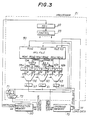
- FIG.3 shows an essential part of the information processing apparatus.
- the information processing apparatus includes an instruction memory 20, a processor 21 and an operand memory 70.
- a 64-bit long instruction word which is read from the instruction memory 20 is stored in an instruction memory 22 within the processor 21.
- Each bit of the long instruction word stored in the instruction memory 22 is supplied to a control circuit 23 within the processor 21.
- FIG.4 shows an embodiment of the control circuit 23 together with the instruction register 22.
- a decoder 25 decodes the bit numbers "0" through “3" of the instruction word stored in the instruction register 22, that is, the type code Type.
- a decoder 26 decodes the bit numbers "4" through “8” of the instruction word together with the type code Type and generates a first operation circuit control signal CNT1.
- a decoder 27 decodes the bit numbers "24" through “28” of the instruction word together with the type code Type and generates a second operation circuit control signal CNT2.
- a decoder 28 decodes the bit numbers "44” through “48” of the instruction word together with the type code Type and generates a third operation circuit control signal CNT3.
- the bit numbers decoded in the decoders 26, 27 and 28 excluding the type code Type respectively correspond to the instruction codes OPa, OPb and OPC of the long instruction word having the first instruction format.
- a selector 24 selects the bit numbers “19” through “23” or the bit numbers “59” through “63” of the instruction word which is stored in the instruction register 22 in response to an output signal of the decoder 25.
- the bits selected by the selector 24 are latched in a latch circuit 29 during an execute cycle.
- the bit numbers "59” through “63” of the instruction word which is stored in the instruction register 22 are latched in a latch circuit 30 during the execute cycle.
- a selector 31 selects the bit numbers "59” through “63” or the bit numbers "39” through “43” of the instruction word which is stored in the instruction register 22 in response to the output signal of the decoder 25.
- the bits selected by the selector 31 are latched in a latch circuit 32 during the execute cycle.
- Outputs of the latch circuits 29, 32 and 30 are respectively latched in latch circuits 35, 36 and 37 during a write cycle, and outputs of the latch circuits 35, 36 and 37 are respectively decoded in decoders 40, 41 and 42.
- the output of the latch circuit 36 is latched in a latch circuit 43 during an access cycle, and an output of the latch circuit 43 is decoded in a decoder 44.
- the decoders 40, 41, 42 and 44 are controlled by portions of the control signals CNT1, CNT2 and CNT3 which are output from the decoders 26, 27 and 28.
- the decoder 40 is enabled in response to an enable signal ENBLA which is obtained by passing the control signal CNT1 through two latch circuits 47 and 48.
- the decoder 41 is enabled in response to an enable signal ENBLB which is obtained by passing the control signal CNT2 through two latch circuits (not shown), and the decoder 42 is enabled in response to an enable signal ENBLC which is obtained by passing the control signal CNT3 through two latch circuits (not shown).
- the decoder 44 is enabled in response to an enable signal ENBLL which is obtained by passing the control signal CNT2 through one latch circuit (not shown).
- the illustration of the latch circuits which are used to obtain the enable signals ENBLB, ENBLC and ENBLL is omitted in FIG.4 in order to simplify the interconnections.
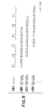
- the processor 21 shown in FIG.3 carries out a pipeline operation.
- a fetch (F) cycle, a decode (D) cycle, an execute (E) cycle and a write (W) cycle of the first long instruction word are carried out as shown in FIG.5(B) in synchronism with a clock signal shown in FIG.5(A).
- the F, D, E and W cycles of the second and third long instruction words are respectively carried out similarly as shown in FIG.5(C) and (D). In other words, the cycles of two successive long instruction words are shifted by one cycle.
- the clock signal shown in FIG.5(A) is supplied to the latch circuits and the like of the processor 21 shown in FIG.3.
- the decoder 25 decodes the type code Type, and the decoder 26. 27 and 28 respectively decode the instructions codes OPa, OPb and OPc together with the type code Type.
- the third register specifying fields Ta3, Rb3 and Rc3 are respectively latched in the latch circuits 29, 32 and 30 during the E cycle.
- the third register specifying fields Ra3, Rb3 and Rc3 are respectively latched in the latch circuits 35, 36 and 37 during the W cycle and decoded in the respective decoders 40, 41 and 42.
- the decoder 25 decodes the type code Type, and the decoders 26 and 27 respectively decode the instruction codes OPa and OPb together with the type code Type.
- the selector 31 selects the bit numbers "59" through "63" of the instruction word which is stored in the instruction register 22 in response to the output signal of the decoder 25, and the third register specifying fields Ra3 and Rb3 are respectively latched in the latch circuits 29 and 32 during the E cycle.
- the bits which are latched in the latch circuits 29 and 32 are respectively latched in the latch circuits 35 and 36 during the W cycle and decoded in the respective decoder 40 and 41.
- the decoder 42 is disabled in response to the enable signal ENBLC. Moreover, the third register specifying field Rb3 which is output from the latch circuit 36 is latched in the latch circuit 43 during the A cycle and is decoded by the decoder 44. This decoder 44 is enabled in response to the enable signal ENBLL only when the instruction word having the format B is a load instruction.
- the decoder 25 decodes the type code Type, and the decoders 26 and 27 respectively decode the instruction codes OPa and OPb together with the type code Type.
- the selector 31 selects the bit numbers "59" through "63" of the instruction word which is stored in the instruction register 22 in response to the output signal of the decoder 25, and the third register specifying fields Ra3 and Rb3 are respectively latched in the latch circuits 29 and 32 during the E cycle.
- the bits which are latched in the latch circuits 29 and 32 are respectively latched in the latch circuits 35 and 36 during the W cycle and decoded in the respective decoders 40 and 41.
- the decoder 42 is disabled in response to the enable signal ENBLC. Moreover, the third register specifying field Rb3 which is output from the latch circuit 36 is latched in the latch circuit 43 during the A cycle and is decoded by the decoder 44. This decoder 44 is enabled in response to the enable signal ENBLL only when the instruction word having the format C is a load instruction.
- the decoder 25 decodes the type code Type, and the decoder 26 decodes the instruction code OPa together wit the type code Type.
- the selector 24 selects the bit numbers "59" through "63" of the instruction word which is stored in the instruction register 22 in response to the output signal of the decoder 25, and the third register specifying field Ra3 is latched in the latch circuit 29 during the E cycle. Furthermore, the bits which are latched in the latch circuit 29 are latched in the latch circuit 35 during the W cycle and decoded by the decoder 40.
- the decoders 41, 42 and 44 are disabled by the respective enable signals ENBLB, ENBLC and ENBLL.
- FIG.6 shows an embodiment of a register file 50 shown in FIG.3.
- 32-bit data applied to each of terminals RIa3, RIb3, RIc3 and RI1 are supplied to all selectors 510 through 5131.
- the selectors 510 through 5131 are all controlled by the outputs of the decoders 40, 41, 42 and 44 shown in FIG.4, and select one of the 32-bit data received from the terminals RIa3, RIb3, RIC3 and RI1.
- Outputs of the selectors 510 through 5131 are respectively supplied to registers R0 through R31.
- the registers R0 through R31 respectively latch the incoming data when the respective clock gate enable signals CGEO through CGE31 are received from the OR circuits 450 through 4531.
- Outputs of the registers R0 through R31 are supplied to all six selectors 52a through 52f.
- the selector 52a is controlled by the bit numbers "9" through “13" of the instruction word which is stored in the instruction register 22, that is, by the first register specifying field Ra1.
- the selector 52b is controlled by the bit numbers "14" through “18” of the instruction word which is stored in the instruction register 22, that is, by the second register specifying field Ra2.
- the selector 52c is controlled by the bit numbers "29” through "33” of the instruction word which is stored in the instruction register 22, that is, by the first register specifying field Rb1.
- the selector 52d is controlled by the bit numbers "34" through “38” of the instruction word which is stored in the instruction register 22, that is, by the second register specifying field Rb2.
- the selector 52e is controlled by the bit numbers "49" through “53” of the instruction word which is stored in the instruction register 22, that is, by the first register specifying field Rc1.
- the selector 52f is controlled by the bit numbers "54" through “58” of the instruction word which is stored in the instruction register 22, that is, by the second register specifying field Rc2.
- the data in the registers R0 through R31 are output from terminals R0a1, R0a2, R0b1, R0b2, R0c1 and R0c2 via the respective selectors 52a through 52f which are selected by the bits of the instruction word stored in the instruction register 22.
- the data received from the terminal R0al of the register file 50 is latched in a latch circuit 55a.
- one of the data received from the terminal R0a2 of the register file 50 and the immediate data IMM32 which corresponds to the bit numbers "9" through “40" of the instruction word which is stored in the instruction register 22 is selected by a selector 54 and latched in a latch circuit 55b.
- the data which are latched in the latch circuits 55a and 55b are subjected to an operation in a first operation circuit 56.
- a result of the operation in the first operation circuit 56 is latched in a latch circuit 57.
- the data received from the terminal R0bl of the register file 50 is latched in a latch circuit 59a.
- one of the data received from the terminal R0b2 of the register file 50, the immediate data IMM25 which corresponds to the bit numbers "34" through “58” of the instruction word which is stored in the instruction register 22 and the immediate data IMM32 which corresponds to the bit numbers "27” through “58” of the instruction word which is stored in the instruction register 22 is selected by a selector 58 and latched in a latch circuit 59b.
- the data which are latched in the latch circuits 59a and 59b are subjected to an operation in a second operation circuit 60. A result of the operation in the second operation circuit 60 is latched in a latch circuit 61.
- the data received from the terminals R0cl and R0c2 of the register file 50 are respectively latched in latch circuits 62a and 62b.
- the data which are latched in the latch circuits 62a and 62b are subjected to an operation in a third operation circuit 63.
- a result of the operation in the third operation circuit 63 is latched in a latch circuit 64.
- the stored data of the registers R0 through R31 which are specified by the register specifying fields Ra1, Ra2, Rb1, Rb2, Rc1 and Rc2 are output from the terminals R0a1, R0a2, R0b1, R0b2, R0c1 and R0c2 of the register file 50.
- the selector 58 by the selection of the output data from the terminal R0b2 by the selector 58, the data described above are latched in the latch circuits 55a, 55b, 59a, 59b, 62a and 62b, and operations are simultaneously carried out in the operation circuits 56, 60 and 63. The results of the operations are respectively applied to the terminals RIa3, RIb3 and RIc3 of the register file 50.
- the stored data of the registers R0 through R31 which are specified by the register specifying fields Ra1, Ra2 and Rb1 are output from the terminals R0a1, R0a2, Rob1 and R0b2 of the register file 50.
- the data described above are latched in the latch circuits 55a, 55b, 59a and 59b, and operations are simultaneously carried out in the operation circuits 56 and 60.
- the results of the operations are respectively applied to the terminals RIa3 and RIb3 of the register file 50.
- the instruction word which has the format B is a load instruction
- the result of the address calculation carried out in the operation circuit 60 is supplied to the operand memory 70, and the load data is supplied from the operand memory 70 to the terminal RIl of the register file 50.
- the stored data of the registers R0 through R31 which are specified by the register specifying fields Ra1, Ra2 and Rb1 are output from the terminals R0a1, R0a2, R0b1 and R0b2 of the register file 50.
- the data described above are latched in the latch circuits 55a, 55b, 59a and 59b, and operations are simultaneously carried out in the operation circuits 56 and 60.
- the results of the operations are respectively applied to the terminals RIa3 and RIb3 of the register file 50.
- the instruction word which has the format B is a load instruction
- the result of the address calculation carried out in the operation circuit 60 is supplied to the operand memory 70, and the load data is supplied from the operand memory 70 to the terminal RI1 of the register file 50.
- the stored data of the registers R0 through R31 which are specified by the register specifying field Ra1 is output from the terminal R0a1 of the register file 50.
- the data described above are latched in the latch circuits 55a and 55b, and an operation is carried out in the operation circuit 56.
- the result of the operation is applied to the terminal RIa3 of the register file 50.
- the instruction word which has the format B is a load instruction
- the result of the address calculation carried out in the operation circuit 60 is supplied to the operand memory 70, and the load data is supplied from the operand memory 70 to the terminal RIl of the register file 50.
- the processor 21 has a 32-bit structure. For this reason, the bit numbers "41" through “58" of the long instruction word having the third format are unused. But when the processor 21 has a 64-bit structure, all of the bit numbers "9” through “58" of the long instruction word having the third format can be used as an immediate data IMM51 ⁇ .
- An instruction address output from a program counter 71 or a branch address output from the latch circuit 61 is selected by a selector 72 and is supplied to the instruction memory 20, so as to read the next long instruction word.
- FIG.7 shows an embodiment of the operation circuit 56 shown in FIG.3.
- the operation circuit 56 includes an arithmetic logic unit (ALU) 56a and a multiplier 56b which are connected as shown.
- ALU arithmetic logic unit
- FIG.8 shows an embodiment of the operation circuit 60 shown in FIG.3.
- the operation circuit 60 includes an ALU 60a and a shift circuit 60b which are connected as shown.
- FIG.9 shows an embodiment of the operation circuit 64 shown in FIG.3.
- the operation circuit 64 includes an ALU 64a.
- the present invention s the unused bits of the long instruction word are eliminated and the bit utilization efficiency is improved by forming the long instruction word which has the fixed length from the type code and one or more instruction words.
- the structure of the instruction words forming the long instruction word that is, the combination of the instruction words forming the long instruction word, is defined by the type code, it becomes possible to simplify both the control of hardware and hardware structure when executing a plurality of instructions in parallel depending on the combination of the instruction words.
Abstract
Description
- The present invention generally relates to instructing methods and execution systems, and more particularly to an instructing method which specifies an instruction which is to be executed in an information processing apparatus and an execution system for executing an instruction in the information processing apparatus.
- Recently, the performance of a processor improved considerably owing to improvements in the integration density of semiconductor devices and operation speeds of the semiconductor devices. However, there is a demand to further improve the performance of the processor. In order to meet this demand, an architecture called reduced instruction set computer (RISC) has been proposed. According to this RISC, an instruction word has a fixed length of 32 bits and the operation is carried out only between registers. In addition, a memory access is restricted only to a transfer between a memory and a register, and the RISC only has instructions with a high frequency of use of programs. By the restrictions described above, it is possible to simplify the hardware which is required to execute the instructions and also simplify the control of the hardware. Hence, the performance of the processor can be improved by increasing the operation clock frequency and reducing the number of cycles required to execute one instruction. On the other hand, there are proposals to simultaneously execute a plurality of instructions so as to further improve the performance of the processor.
- FIGS.1A, 1B and 1C show examples of instruction formats used in the conventional RISC architecture.
- FIG.1A shows an instruction having a first format. Based on an instruction code OP, this instruction instructs an operation between a register content specified by a second register instruction field R2X and a register content specified by a third register instruction field R3X and a storage of an operation result in a register specified by a first register instruction field R1X.
- FIG.1B shows an instruction having a second format. When this instruction is an operation instruction, this instruction instructs an operation between the register content specified,by the second register instruction field R2X and 16-bit immediate data IMM16 and a storage of an operation result in the register specified by the first register instruction field RIX. On the other hand, when this instruction is a load instruction, this instruction instructs an addition of an address which is the register content specified by the second register instruction field R2X and a deviation which is given as the immediate data IMM16 and a storage of the data of the address of the memory obtained by the addition in the register specified by the first register specifying field R1X.
- FIG.1C shows an instruction having a third format. This instruction instructs a storage of a 21-bit immediate data IMM21 in the register specified by the first register specifying field R1X.
- According to the instruction having the first format, the twenty-first through thirty-first bits are unused and there is a problem in that the bit utilization efficiency is poor. On the other hand, according to the instruction having the second format, there is a problem in that a plurality of instructions must be used when large immediate data and deviation are required, such as the case where the immediate data exceeds 16 bits. Similarly, according to the instruction having the third format, there is a problem in that a plurality of instructions must be used when a large immediate data is required, such as the case where the immediate data exceeds 21 bits.
- Furthermore, when executing a plurality of instructions in parallel, the control the hardware becomes complex and the scale of the hardware structure required to execute the instructions in parallel becomes large because there exist a large number of combinations of instructions which must be executed in parallel.
- Accordingly, it is a general object of the present invention to provide novel and useful instructing method and execution system in which the problems described above are eliminated.
- Another and more specific object of the present invention is to provide an instructing method for specifying an instruction which is to be executed in an information processing apparatus, comprising the steps of forming each of instruction words from at least an instruction code and an operand specifying part, for specifying a single instruction, forming each of long instruction words having a fixed length from a type code and one or plurality of the instruction words, where the type code specifies a structure of the one or plurality of the instruction words included in the long instruction word, and specifying one or plurality of instructions by a the long instruction word. According to the instructing method of the present invention, it is possible to reduce the unused bits of the instruction words and improve the bit utilization efficiency. Furthermore, it is possible to specify even a large immediate data by a single long instruction word.
- Still another object of the present invention is to provide an execution system for executing instructions in an information processing apparatus, comprising input means for inputting a long instruction word which has a fixed length, where the long instruction word is made up of a type code and one or a plurality of instruction words, each of the instruction words include at least an instruction code and an operand specifying part for specifying a single instruction and the type code specifies a structure of the one or plurality of the instruction words included in the long instruction word, judging means coupled to the input means for judging from the type code a combination and a number of the instruction words included in the long instruction word and for outputting a judgement result, a plurality of operation means coupled to the judging means for independently carrying out operations specified by the instruction words included in the long instruction word, and assigning means coupled to the judging means for assigning an operation specified by each instruction word included in the long instruction word to one of the operation means depending on the judgement result output from the judging means. According to the execution system of the present invention, it is possible to simplify both the control of hardware and hardware structure.
- Other objects and further features of the present invention will be apparent from the following detailed description when read in conjunction with the accompanying drawings.
-
- FIGS.1A, 1B and 1C respectively are diagrams showing examples of instruction formats used in the conventional RISC architecture;
- FIGS.2A, 2B, 2C and 2D respectively are diagrams showing embodiments of instruction formats used in the present invention;
- FIG.3 is a system block diagram showing an essential part of an information processing apparatus which is applied with the present invention;
- FIG.4 is a system block diagram showing an embodiment of a control circuit shown in FIG.3 together with an instruction register;
- FIG.5 is a timing chart for explaining a pipeline operation of a processor shown in FIG.3;
- FIG.6 is a system block diagram showing an embodiment of a register file shown in FIG.3; and
- FIG.7, 8 and 9 are block diagrams respectively showing embodiments of operation circuits shown in FIG.3.
- First, a description will be given of embodiments of instruction formats which may be used in the present invention, by referring to FIGS.2A through 2D.
- FIG.2A shows a 64-bit long instruction word having a first instruction format. This long instruction word is made up of a type code Type arranged at bit numbers "0" through "3", and three instruction words having a format A and respectively arranged at bit numbers "4" through "23", "24" through "43", and "44" through "63".
- The instruction word having the format A and arranged at the bit numbers "4" through "23" includes a 5-bit instruction code OPa, a 5-bit first register specifying field Ra1, a 5-bit second register specifying field Ra2 and a 5-bit third register specifying field Ra3. The register specifying fields Ra1, Ra2 and Ra3 are provided as an operand specifying part. This instruction word instructs an operation between a register content specified by the first register specifying field Ra1 and a register content specified by the second register specifying field Ra2 and a storage of an operation result in a register specified by the third register specifying field Ra3 depending on the instruction code OPa.
- The instruction word having the format A and arranged at the bit numbers "24" through "43" includes a 5-bit instruction code OPb, a 5-bit first register specifying field Rb1, a 5-bit second register specifying field Rb2 and a 5-bit third register specifying field Rb3. The register specifying fields Rb1, Rb2 and Rb3 are provided as an operand specifying part. This instruction word instructs an operation between a register content specified by the first register specifying field Rb1 and a register content specified by the second register specifying field Rb2 and a storage of an operation result in a register specified by the third register specifying field Rb3 depending on the instruction code OPb.
- Similarly, the instruction word having the format A and arranged at the bit numbers "44" through "63" includes a 5-bit instruction code OPc, a 5-bit first register specifying field Rc1, a 5-bit second register specifying field Rc2 and a 5-bit third register specifying field Rc3. The register specifying fields Rc1, Rc2 and Rc3 are provided as an operand specifying part. This instruction word instructs an operation between a register content specified by the first register specifying field Rc1 and a register content specified by the second register specifying field Rc2 and a storage of an operation result in a register specified by the third register specifying field Rc3 depending on the instruction code OPc.
- The kind of operation to be carried out is specified by a combination of the 4-bit type code Type and one of the 5-bit instruction codes OPa, OPb and OPc. The kind of operation to be carried out is similarly specified for the long instruction words shown in FIGS.2B through 2D which will be described hereunder.
- FIG.2B shows a 64-bit long instruction word having a second instruction format. This long instruction word is made up of a type code Type arranged at bit numbers "0" through "3", an instruction word having the format A and arranged at bit numbers "4" through "23", and an instruction word having a format B and arranged at bit numbers "24" through "63".
- The instruction word having the format A and arranged at the bit numbers "4" through "23" includes the 5-bit instruction code OPa, the 5-bit first register specifying field Ra1, the 5-bit second register specifying field Ra2 and the 5-bit third register specifying field Ra3. The register specifying fields Ra1, Ra2 and Ra3 are provided as the operand specifying part. This instruction word instructs an operation between the register content specified by the first register specifying field Ra1 and the register content specified by the second register specifying field Ra2 and a storage of an operation result in the register specified by the third register specifying field Ra3 depending on the instruction code OPa.
- The instruction word having the format B and arranged at the bit numbers "24" through "63" includes the 5-bit instruction code OPb, the 5-bit first register specifying field Rb1, a 25-bit immediate data IMM25 and the 5-bit third register specifying field Rb3. The first register specifying field Rb1 is arranged at the bit numbers "29" through "33", the immediate data IMM25 is arranged at the bit numbers "34" through "58", and the third register specifying field Rb3 is arranged at the bit numbers "59" through "63". When the instruction code OPb represents an operation instruction, this instruction word instructs an operation between the register content specified by the first register specifying field Rb1 and the immediate data IMM25 and a storage of an operation result in the register specified by the third register specifying field Rb3 depending on the instruction code OPb. On the other hand, when the instruction code OPb represents a load instructions this instruction word instructs an addition of an address which is the register content specified by the first register specifying field Rb1 and a deviation which is given as the immediate data IMM25 and a storage of the data of the address of the memory obtained by the addition in the register specified by the third register specifying field Rb3 depending on the instruction code OPb.
- FIG.2C shows a 64-bit long instruction word having a third instruction format. This long instruction word is made up of a type code Type arranged at bit numbers "0" through "3", an instruction word having the format A and arranged at bit numbers "4" through "23", and an instruction word having a format C and arranged at bit numbers "24" through "63".
- The instruction word having the format A and arranged at the bit numbers "4" through "23" includes the 5-bit instruction code OPa, the 5-bit first register specifying field Ra1, the 5-bit second register specifying field Ra2 and the 5-bit third register specifying field Ra3. The register specifying fields Ra1, Ra2 and Ra3 are provided as the operand specifying part. This instruction word instructs an operation between the register content specified by the first register specifying field Ra1 and the register content specified by the second register specifying field Ra2 and a storage of an operation result in the register specified by the third register specifying field Ra3 depending on the instruction code OPa.
- The instruction word having the format C and arranged at the bit numbers "24" through "63" includes the 5-bit instruction code OPb, a 32-bit immediate data IMM32 and the 5-bit third register specifying field Rb3. The immediate data IMM32 is arranged at the bit numbers "27" through "58", and the third register specifying field Rb3 is arranged at the bit numbers "59" through "63". This instruction word instructs a storage of immediate data IMM32 in the register specified by the third register specifying field Rb3 depending on the instruction code OPb.
- FIG.2D shows a 64-bit long instruction word having a fourth instruction format. This long instruction word is made up of a type code Type arranged at bit numbers "0" through "3", and a 60-bit instruction word having the format D and arranged at bit numbers "4" through "23" through "63".
- The instruction word having the format D and arranged at the bit numbers "4" through "63" includes the 5-bit instruction code OPa, the 32-bit immediate data IMM32 and the 5-bit third register specifying field Rb3. The immediate data IMM32 is arranged at the bit numbers "9" through "40", and the third register specifying field Rb3 is arranged at the bit numbers "59" through "63". This instruction word instructs a storage of immediate data IMM32 in the register specified by the third register specifying field Rb3 depending on the instruction code OPa.
- In the long instruction words shown in FIGS.2A through 2D, the formats A through D of the instruction words are distinguished from the value of the type code Type.
- Next, a description will be given of an information processing apparatus which is applied with an embodiment of the instructing method according to the present invention and an embodiment of the execution system according to the present invention, by referring to FIG.3.
- FIG.3 shows an essential part of the information processing apparatus. The information processing apparatus includes an
instruction memory 20, aprocessor 21 and an operand memory 70. A 64-bit long instruction word which is read from theinstruction memory 20 is stored in aninstruction memory 22 within theprocessor 21. Each bit of the long instruction word stored in theinstruction memory 22 is supplied to acontrol circuit 23 within theprocessor 21. - FIG.4 shows an embodiment of the
control circuit 23 together with theinstruction register 22. Adecoder 25 decodes the bit numbers "0" through "3" of the instruction word stored in theinstruction register 22, that is, the type code Type. Adecoder 26 decodes the bit numbers "4" through "8" of the instruction word together with the type code Type and generates a first operation circuit control signal CNT1. Adecoder 27 decodes the bit numbers "24" through "28" of the instruction word together with the type code Type and generates a second operation circuit control signal CNT2. Similarly, adecoder 28 decodes the bit numbers "44" through "48" of the instruction word together with the type code Type and generates a third operation circuit control signal CNT3. The bit numbers decoded in thedecoders - A
selector 24 selects the bit numbers "19" through "23" or the bit numbers "59" through "63" of the instruction word which is stored in theinstruction register 22 in response to an output signal of thedecoder 25. The bits selected by theselector 24 are latched in alatch circuit 29 during an execute cycle. The bit numbers "59" through "63" of the instruction word which is stored in theinstruction register 22 are latched in alatch circuit 30 during the execute cycle. Aselector 31 selects the bit numbers "59" through "63" or the bit numbers "39" through "43" of the instruction word which is stored in theinstruction register 22 in response to the output signal of thedecoder 25. The bits selected by theselector 31 are latched in alatch circuit 32 during the execute cycle. - Outputs of the
latch circuits latch circuits latch circuits decoders latch circuit 36 is latched in alatch circuit 43 during an access cycle, and an output of thelatch circuit 43 is decoded in adecoder 44. Thedecoders decoders latch circuits decoder 41 is enabled in response to an enable signal ENBLB which is obtained by passing the control signal CNT2 through two latch circuits (not shown), and thedecoder 42 is enabled in response to an enable signal ENBLC which is obtained by passing the control signal CNT3 through two latch circuits (not shown). Thedecoder 44 is enabled in response to an enable signal ENBLL which is obtained by passing the control signal CNT2 through one latch circuit (not shown). The illustration of the latch circuits which are used to obtain the enable signals ENBLB, ENBLC and ENBLL is omitted in FIG.4 in order to simplify the interconnections. - Thirty-two OR
circuits 45₀ through 45₃₁ respectively generate clock gate enable signals CGEO through CGE31 based on the outputs of thedecoders - The
processor 21 shown in FIG.3 carries out a pipeline operation. In this case, a fetch (F) cycle, a decode (D) cycle, an execute (E) cycle and a write (W) cycle of the first long instruction word are carried out as shown in FIG.5(B) in synchronism with a clock signal shown in FIG.5(A). The F, D, E and W cycles of the second and third long instruction words are respectively carried out similarly as shown in FIG.5(C) and (D). In other words, the cycles of two successive long instruction words are shifted by one cycle. - However, in the case of the load instruction within the long instruction word, an address calculation is carried out in place of the E cycle and a memory access (access (A) cycle) is made in place of the W cycle. 5(A) is supplied
- The clock signal shown in FIG.5(A) is supplied to the latch circuits and the like of the
processor 21 shown in FIG.3. - When the long instruction word of the first format is stored in the
instruction register 22, thedecoder 25 decodes the type code Type, and thedecoder 26. 27 and 28 respectively decode the instructions codes OPa, OPb and OPc together with the type code Type. In addition, the third register specifying fields Ta3, Rb3 and Rc3 are respectively latched in thelatch circuits latch circuits respective decoders - When the long instruction word of the second format is stored in the
instruction register 22, thedecoder 25 decodes the type code Type, and thedecoders selector 31 selects the bit numbers "59" through "63" of the instruction word which is stored in theinstruction register 22 in response to the output signal of thedecoder 25, and the third register specifying fields Ra3 and Rb3 are respectively latched in thelatch circuits latch circuits latch circuits respective decoder 40 and 41. Thedecoder 42 is disabled in response to the enable signal ENBLC. Moreover, the third register specifying field Rb3 which is output from thelatch circuit 36 is latched in thelatch circuit 43 during the A cycle and is decoded by thedecoder 44. Thisdecoder 44 is enabled in response to the enable signal ENBLL only when the instruction word having the format B is a load instruction. - When the long instruction word having the third format is stored in the
instruction register 22, thedecoder 25 decodes the type code Type, and thedecoders selector 31 selects the bit numbers "59" through "63" of the instruction word which is stored in theinstruction register 22 in response to the output signal of thedecoder 25, and the third register specifying fields Ra3 and Rb3 are respectively latched in thelatch circuits latch circuits latch circuits respective decoders 40 and 41. Thedecoder 42 is disabled in response to the enable signal ENBLC. Moreover, the third register specifying field Rb3 which is output from thelatch circuit 36 is latched in thelatch circuit 43 during the A cycle and is decoded by thedecoder 44. Thisdecoder 44 is enabled in response to the enable signal ENBLL only when the instruction word having the format C is a load instruction. - When the long instruction word having the fourth format is stored in the
instruction register 22, thedecoder 25 decodes the type code Type, and thedecoder 26 decodes the instruction code OPa together wit the type code Type. In addition, theselector 24 selects the bit numbers "59" through "63" of the instruction word which is stored in theinstruction register 22 in response to the output signal of thedecoder 25, and the third register specifying field Ra3 is latched in thelatch circuit 29 during the E cycle. Furthermore, the bits which are latched in thelatch circuit 29 are latched in thelatch circuit 35 during the W cycle and decoded by the decoder 40. Thedecoders - FIG.6 shows an embodiment of a
register file 50 shown in FIG.3. In FIG.6, 32-bit data applied to each of terminals RIa3, RIb3, RIc3 and RI1 are supplied to allselectors 51₀ through 51₃₁. Theselectors 51₀ through 51₃₁ are all controlled by the outputs of thedecoders selectors 51₀ through 51₃₁ are respectively supplied to registers R0 through R31. The registers R0 through R31 respectively latch the incoming data when the respective clock gate enable signals CGEO through CGE31 are received from theOR circuits 45₀ through 45₃₁. - Outputs of the registers R0 through R31 are supplied to all six
selectors 52a through 52f. Theselector 52a is controlled by the bit numbers "9" through "13" of the instruction word which is stored in theinstruction register 22, that is, by the first register specifying field Ra1. Theselector 52b is controlled by the bit numbers "14" through "18" of the instruction word which is stored in theinstruction register 22, that is, by the second register specifying field Ra2. The selector 52c is controlled by the bit numbers "29" through "33" of the instruction word which is stored in theinstruction register 22, that is, by the first register specifying field Rb1. Theselector 52d is controlled by the bit numbers "34" through "38" of the instruction word which is stored in theinstruction register 22, that is, by the second register specifying field Rb2. Theselector 52e is controlled by the bit numbers "49" through "53" of the instruction word which is stored in theinstruction register 22, that is, by the first register specifying field Rc1. Theselector 52f is controlled by the bit numbers "54" through "58" of the instruction word which is stored in theinstruction register 22, that is, by the second register specifying field Rc2. The data in the registers R0 through R31 are output from terminals R0a1, R0a2, R0b1, R0b2, R0c1 and R0c2 via therespective selectors 52a through 52f which are selected by the bits of the instruction word stored in theinstruction register 22. - Returning now to the description of FIG.3, the data received from the terminal R0al of the
register file 50 is latched in alatch circuit 55a. On the other hand, one of the data received from the terminal R0a2 of theregister file 50 and the immediate data IMM32 which corresponds to the bit numbers "9" through "40" of the instruction word which is stored in theinstruction register 22 is selected by aselector 54 and latched in alatch circuit 55b. The data which are latched in thelatch circuits first operation circuit 56. A result of the operation in thefirst operation circuit 56 is latched in alatch circuit 57. - The data received from the terminal R0bl of the
register file 50 is latched in alatch circuit 59a. On the other hand, one of the data received from the terminal R0b2 of theregister file 50, the immediate data IMM25 which corresponds to the bit numbers "34" through "58" of the instruction word which is stored in theinstruction register 22 and the immediate data IMM32 which corresponds to the bit numbers "27" through "58" of the instruction word which is stored in theinstruction register 22 is selected by a selector 58 and latched in alatch circuit 59b. The data which are latched in thelatch circuits second operation circuit 60. A result of the operation in thesecond operation circuit 60 is latched in alatch circuit 61. - The data received from the terminals R0cl and R0c2 of the
register file 50 are respectively latched in latch circuits 62a and 62b. The data which are latched in the latch circuits 62a and 62b are subjected to an operation in athird operation circuit 63. A result of the operation in thethird operation circuit 63 is latched in alatch circuit 64. - When executing the long instruction word having the first format, the stored data of the registers R0 through R31 which are specified by the register specifying fields Ra1, Ra2, Rb1, Rb2, Rc1 and Rc2 are output from the terminals R0a1, R0a2, R0b1, R0b2, R0c1 and R0c2 of the
register file 50. In addition, by the selection of the output data from the terminal R0b2 by the selector 58, the data described above are latched in thelatch circuits operation circuits register file 50. - When executing the long instruction word having the second format, the stored data of the registers R0 through R31 which are specified by the register specifying fields Ra1, Ra2 and Rb1 are output from the terminals R0a1, R0a2, Rob1 and R0b2 of the
register file 50. In addition, by the selection of the immediate data IMM25 by the selector 58, the data described above are latched in thelatch circuits operation circuits register file 50. However, when the instruction word which has the format B is a load instruction, the result of the address calculation carried out in theoperation circuit 60 is supplied to the operand memory 70, and the load data is supplied from the operand memory 70 to the terminal RIl of theregister file 50. - When executing the long instruction word having the third format, the stored data of the registers R0 through R31 which are specified by the register specifying fields Ra1, Ra2 and Rb1 are output from the terminals R0a1, R0a2, R0b1 and R0b2 of the
register file 50. In addition, by the selection of the immediate data IMM32 by the selector 58, the data described above are latched in thelatch circuits operation circuits register file 50. However, when the instruction word which has the format B is a load instruction, the result of the address calculation carried out in theoperation circuit 60 is supplied to the operand memory 70, and the load data is supplied from the operand memory 70 to the terminal RI1 of theregister file 50. - When executing the long instruction word having the fourth format, the stored data of the registers R0 through R31 which are specified by the register specifying field Ra1 is output from the terminal R0a1 of the
register file 50. In addition, by the selection of the immediate data IMM32 by theselector 54, the data described above are latched in thelatch circuits operation circuit 56. The result of the operation is applied to the terminal RIa3 of theregister file 50. However, when the instruction word which has the format B is a load instruction, the result of the address calculation carried out in theoperation circuit 60 is supplied to the operand memory 70, and the load data is supplied from the operand memory 70 to the terminal RIl of theregister file 50. In this embodiment, theprocessor 21 has a 32-bit structure. For this reason, the bit numbers "41" through "58" of the long instruction word having the third format are unused. But when theprocessor 21 has a 64-bit structure, all of the bit numbers "9" through "58" of the long instruction word having the third format can be used as an immediate data IMM51`. - An instruction address output from a
program counter 71 or a branch address output from thelatch circuit 61 is selected by aselector 72 and is supplied to theinstruction memory 20, so as to read the next long instruction word. - FIG.7 shows an embodiment of the
operation circuit 56 shown in FIG.3. Theoperation circuit 56 includes an arithmetic logic unit (ALU) 56a and amultiplier 56b which are connected as shown. - FIG.8 shows an embodiment of the
operation circuit 60 shown in FIG.3. Theoperation circuit 60 includes anALU 60a and ashift circuit 60b which are connected as shown. - FIG.9 shows an embodiment of the
operation circuit 64 shown in FIG.3. Theoperation circuit 64 includes an ALU 64a. - By restricting the instruction codes OPa, OPb and OPC of the long instruction words having the first through fourth formats to only those instructions which can be carried out in the
operation circuits - Therefore, according to the present inventions the unused bits of the long instruction word are eliminated and the bit utilization efficiency is improved by forming the long instruction word which has the fixed length from the type code and one or more instruction words. In addition, it becomes possible to specify a large immediate data by reducing the number of instruction words included in the long instruction word. Furthermore, since the structure of the instruction words forming the long instruction word, that is, the combination of the instruction words forming the long instruction word, is defined by the type code, it becomes possible to simplify both the control of hardware and hardware structure when executing a plurality of instructions in parallel depending on the combination of the instruction words.
- Further, the present invention is not limited to these embodiments, but various variations and modifications may be made without departing from the scope of the present invention.
Claims (10)
forming each of instruction words from at least an instruction code (OPa, OPb, OPC) and an operand specifying part (Ra1-Rac, Rb1-Rb3, Rc1-Rc3), for specifying a single instruction;
forming each of long instruction words having a fixed length from a type code (Type) and one or plurality of said instruction words, said type code specifying a structure of the one or plurality of said instruction words included in the long instruction word; and
specifying one or plurality of instructions by a said long instruction word.
input means (22) for inputting a long instruction word which has a fixed length, said long instruction word being made up of a type code (Type) and one or a plurality of instruction words, each of said instruction words including at least an instruction code (OPa, OPb, OPC) and an operand specifying part (Ra1-Ra3, Rb1-Rb3, Rc1-Rc3) for specifying a single instruction, said type code specifying a structure of the one or plurality of said instruction words included in the long instruction word;
judging means (23) coupled to said input means for judging from the type code a combination and a number of the instruction words included in the long instruction word and for outputting a judgement result;
a plurality of operation means (56, 60, 63) coupled to said judging means for independently carrying out operations specified by the instruction words included in the long instruction word; and
assigning means (23, 54, 58) coupled to said judging means for assigning an operation specified by each instruction word included in the long instruction word to one of said operation means depending on the judgement result output from said judging means.
Applications Claiming Priority (2)
| Application Number | Priority Date | Filing Date | Title |
|---|---|---|---|
| JP1285471A JP2835103B2 (en) | 1989-11-01 | 1989-11-01 | Instruction designation method and instruction execution method |
| JP285471/89 | 1989-11-01 |
Publications (3)
| Publication Number | Publication Date |
|---|---|
| EP0426393A2 true EP0426393A2 (en) | 1991-05-08 |
| EP0426393A3 EP0426393A3 (en) | 1991-08-07 |
| EP0426393B1 EP0426393B1 (en) | 1998-01-07 |
Family
ID=17691950
Family Applications (1)
| Application Number | Title | Priority Date | Filing Date |
|---|---|---|---|
| EP90311767A Expired - Lifetime EP0426393B1 (en) | 1989-11-01 | 1990-10-26 | Instructing method and execution system |
Country Status (7)
| Country | Link |
|---|---|
| US (1) | US5442762A (en) |
| EP (1) | EP0426393B1 (en) |
| JP (1) | JP2835103B2 (en) |
| KR (1) | KR930007041B1 (en) |
| AU (1) | AU625008B2 (en) |
| CA (1) | CA2029088C (en) |
| DE (1) | DE69031899T2 (en) |
Cited By (21)
| Publication number | Priority date | Publication date | Assignee | Title |
|---|---|---|---|---|
| WO1993001545A1 (en) * | 1991-07-08 | 1993-01-21 | Seiko Epson Corporation | High-performance risc microprocessor architecture |
| EP0551090A2 (en) * | 1992-01-06 | 1993-07-14 | Hitachi, Ltd. | Computer having a parallel operating capability |
| US5448705A (en) * | 1991-07-08 | 1995-09-05 | Seiko Epson Corporation | RISC microprocessor architecture implementing fast trap and exception state |
| US5560032A (en) * | 1991-07-08 | 1996-09-24 | Seiko Epson Corporation | High-performance, superscalar-based computer system with out-of-order instruction execution and concurrent results distribution |
| EP0741358A2 (en) * | 1995-05-02 | 1996-11-06 | Hitachi, Ltd. | Microcomputer |
| EP0886210A2 (en) * | 1997-06-16 | 1998-12-23 | Matsushita Electric Industrial Co., Ltd. | Processor for executing highly efficient VLIW instructions |
| EP0942357A2 (en) * | 1998-03-11 | 1999-09-15 | Matsushita Electric Industrial Co., Ltd. | Data processor compatible with a plurality of instruction formats |
| US5961629A (en) * | 1991-07-08 | 1999-10-05 | Seiko Epson Corporation | High performance, superscalar-based computer system with out-of-order instruction execution |
| US5983334A (en) * | 1992-03-31 | 1999-11-09 | Seiko Epson Corporation | Superscalar microprocessor for out-of-order and concurrently executing at least two RISC instructions translating from in-order CISC instructions |
| EP0974894A2 (en) * | 1993-11-05 | 2000-01-26 | Intergraph Corporation | Instruction cache associative cross-bar switch |
| EP0992892A1 (en) * | 1998-10-06 | 2000-04-12 | Texas Instruments Inc. | Compound memory access instructions |
| WO2000022515A1 (en) * | 1998-10-14 | 2000-04-20 | Conexant Systems, Inc. | Reconfigurable functional units for implementing a hybrid vliw-simd programming model |
| EP1089186A2 (en) * | 1999-10-01 | 2001-04-04 | STMicroelectronics, Inc. | Method and apparatus for ransmiting operation packets between functional modules of a processor |
| EP0897147A3 (en) * | 1997-06-16 | 2001-10-10 | Matsushita Electric Industrial Co., Ltd. | Constant reconstructing processor which supports reductions in code size |
| US6360313B1 (en) | 1993-11-05 | 2002-03-19 | Intergraph Corporation | Instruction cache associative crossbar switch |
| US6681319B1 (en) | 1998-10-06 | 2004-01-20 | Texas Instruments Incorporated | Dual access instruction and compound memory access instruction with compatible address fields |
| US7000097B2 (en) | 1992-09-29 | 2006-02-14 | Seiko Epson Corporation | System and method for handling load and/or store operations in a superscalar microprocessor |
| KR100636596B1 (en) | 2004-11-25 | 2006-10-23 | 한국전자통신연구원 | Parallel Data Path Architecture for High Energy Efficient |
| EP1628213A3 (en) * | 1997-08-29 | 2009-01-07 | Panasonic Corporation | VLIW processor |
| US7844797B2 (en) | 1992-09-29 | 2010-11-30 | Seiko Epson Corporation | System and method for handling load and/or store operations in a superscalar microprocessor |
| US9678754B2 (en) | 2010-03-03 | 2017-06-13 | Qualcomm Incorporated | System and method of processing hierarchical very long instruction packets |
Families Citing this family (38)
| Publication number | Priority date | Publication date | Assignee | Title |
|---|---|---|---|---|
| JP2746775B2 (en) * | 1991-08-05 | 1998-05-06 | シャープ株式会社 | Central processing unit |
| JPH05100897A (en) * | 1991-10-03 | 1993-04-23 | Agency Of Ind Science & Technol | Instruction trace system |
| WO1994027216A1 (en) * | 1993-05-14 | 1994-11-24 | Massachusetts Institute Of Technology | Multiprocessor coupling system with integrated compile and run time scheduling for parallelism |
| US5860085A (en) * | 1994-08-01 | 1999-01-12 | Cypress Semiconductor Corporation | Instruction set for a content addressable memory array with read/write circuits and an interface register logic block |
| US6397262B1 (en) | 1994-10-14 | 2002-05-28 | Qnx Software Systems, Ltd. | Window kernel |
| US5745759A (en) * | 1994-10-14 | 1998-04-28 | Qnx Software Systems, Ltd. | Window kernel |
| JP2931890B2 (en) | 1995-07-12 | 1999-08-09 | 三菱電機株式会社 | Data processing device |
| US5848288A (en) * | 1995-09-20 | 1998-12-08 | Intel Corporation | Method and apparatus for accommodating different issue width implementations of VLIW architectures |
| US5864704A (en) * | 1995-10-10 | 1999-01-26 | Chromatic Research, Inc. | Multimedia processor using variable length instructions with opcode specification of source operand as result of prior instruction |
| JP3201716B2 (en) * | 1996-02-22 | 2001-08-27 | シャープ株式会社 | Computer equipment |
| US5867681A (en) * | 1996-05-23 | 1999-02-02 | Lsi Logic Corporation | Microprocessor having register dependent immediate decompression |
| US5794010A (en) * | 1996-06-10 | 1998-08-11 | Lsi Logic Corporation | Method and apparatus for allowing execution of both compressed instructions and decompressed instructions in a microprocessor |
| US5896519A (en) * | 1996-06-10 | 1999-04-20 | Lsi Logic Corporation | Apparatus for detecting instructions from a variable-length compressed instruction set having extended and non-extended instructions |
| US5890009A (en) * | 1996-12-12 | 1999-03-30 | International Business Machines Corporation | VLIW architecture and method for expanding a parcel |
| JP3412462B2 (en) | 1997-07-30 | 2003-06-03 | 松下電器産業株式会社 | Processor |
| US6012138A (en) * | 1997-12-19 | 2000-01-04 | Lsi Logic Corporation | Dynamically variable length CPU pipeline for efficiently executing two instruction sets |
| US6112299A (en) * | 1997-12-31 | 2000-08-29 | International Business Machines Corporation | Method and apparatus to select the next instruction in a superscalar or a very long instruction word computer having N-way branching |
| US6081884A (en) * | 1998-01-05 | 2000-06-27 | Advanced Micro Devices, Inc. | Embedding two different instruction sets within a single long instruction word using predecode bits |
| US6076154A (en) * | 1998-01-16 | 2000-06-13 | U.S. Philips Corporation | VLIW processor has different functional units operating on commands of different widths |
| US6324639B1 (en) | 1998-03-30 | 2001-11-27 | Matsushita Electric Industrial Co., Ltd. | Instruction converting apparatus using parallel execution code |
| US6237076B1 (en) * | 1998-08-19 | 2001-05-22 | International Business Machines Corporation | Method for register renaming by copying a 32 bits instruction directly or indirectly to a 64 bits instruction |
| US8171263B2 (en) * | 1999-04-09 | 2012-05-01 | Rambus Inc. | Data processing apparatus comprising an array controller for separating an instruction stream processing instructions and data transfer instructions |
| US8169440B2 (en) | 1999-04-09 | 2012-05-01 | Rambus Inc. | Parallel data processing apparatus |
| US7802079B2 (en) | 1999-04-09 | 2010-09-21 | Clearspeed Technology Limited | Parallel data processing apparatus |
| JP5285828B2 (en) | 1999-04-09 | 2013-09-11 | ラムバス・インコーポレーテッド | Parallel data processor |
| US7966475B2 (en) | 1999-04-09 | 2011-06-21 | Rambus Inc. | Parallel data processing apparatus |
| US20080008393A1 (en) * | 1999-04-09 | 2008-01-10 | Dave Stuttard | Parallel data processing apparatus |
| US8174530B2 (en) * | 1999-04-09 | 2012-05-08 | Rambus Inc. | Parallel date processing apparatus |
| US7526630B2 (en) * | 1999-04-09 | 2009-04-28 | Clearspeed Technology, Plc | Parallel data processing apparatus |
| US8762691B2 (en) | 1999-04-09 | 2014-06-24 | Rambus Inc. | Memory access consolidation for SIMD processing elements using transaction identifiers |
| US20080162874A1 (en) * | 1999-04-09 | 2008-07-03 | Dave Stuttard | Parallel data processing apparatus |
| US20070242074A1 (en) * | 1999-04-09 | 2007-10-18 | Dave Stuttard | Parallel data processing apparatus |
| US20080162875A1 (en) * | 1999-04-09 | 2008-07-03 | Dave Stuttard | Parallel Data Processing Apparatus |
| US6675285B1 (en) * | 2000-04-21 | 2004-01-06 | Ati International, Srl | Geometric engine including a computational module without memory contention |
| US6633969B1 (en) | 2000-08-11 | 2003-10-14 | Lsi Logic Corporation | Instruction translation system and method achieving single-cycle translation of variable-length MIPS16 instructions |
| US8495341B2 (en) * | 2010-02-17 | 2013-07-23 | International Business Machines Corporation | Instruction length based cracking for instruction of variable length storage operands |
| US20110314263A1 (en) * | 2010-06-22 | 2011-12-22 | International Business Machines Corporation | Instructions for performing an operation on two operands and subsequently storing an original value of operand |
| JP5625903B2 (en) * | 2010-12-29 | 2014-11-19 | 富士通株式会社 | Arithmetic processing apparatus and arithmetic processing method |
Citations (1)
| Publication number | Priority date | Publication date | Assignee | Title |
|---|---|---|---|---|
| EP0363222A2 (en) * | 1988-10-07 | 1990-04-11 | Hewlett-Packard Company | Method and apparatus for concurrent dispatch of instructions to multiple functional units |
Family Cites Families (9)
| Publication number | Priority date | Publication date | Assignee | Title |
|---|---|---|---|---|
| US4488219A (en) * | 1982-03-18 | 1984-12-11 | International Business Machines Corporation | Extended control word decoding |
| US4569016A (en) * | 1983-06-30 | 1986-02-04 | International Business Machines Corporation | Mechanism for implementing one machine cycle executable mask and rotate instructions in a primitive instruction set computing system |
| US5179680A (en) * | 1987-04-20 | 1993-01-12 | Digital Equipment Corporation | Instruction storage and cache miss recovery in a high speed multiprocessing parallel processing apparatus |
| US5036454A (en) * | 1987-05-01 | 1991-07-30 | Hewlett-Packard Company | Horizontal computer having register multiconnect for execution of a loop with overlapped code |
| JP2635057B2 (en) * | 1987-11-04 | 1997-07-30 | 株式会社日立製作所 | Microprocessor |
| US5115500A (en) * | 1988-01-11 | 1992-05-19 | International Business Machines Corporation | Plural incompatible instruction format decode method and apparatus |
| US5202967A (en) * | 1988-08-09 | 1993-04-13 | Matsushita Electric Industrial Co., Ltd. | Data processing apparatus for performing parallel decoding and parallel execution of a variable word length instruction |
| US5293592A (en) * | 1989-04-07 | 1994-03-08 | Intel Corporatino | Decoder for pipelined system having portion indicating type of address generation and other portion controlling address generation within pipeline |
| US5197137A (en) * | 1989-07-28 | 1993-03-23 | International Business Machines Corporation | Computer architecture for the concurrent execution of sequential programs |
-
1989
- 1989-11-01 JP JP1285471A patent/JP2835103B2/en not_active Expired - Fee Related
-
1990
- 1990-10-26 EP EP90311767A patent/EP0426393B1/en not_active Expired - Lifetime
- 1990-10-26 DE DE69031899T patent/DE69031899T2/en not_active Expired - Fee Related
- 1990-10-31 CA CA002029088A patent/CA2029088C/en not_active Expired - Fee Related
- 1990-10-31 AU AU65722/90A patent/AU625008B2/en not_active Ceased
- 1990-11-01 KR KR1019900017654A patent/KR930007041B1/en not_active IP Right Cessation
-
1994
- 1994-02-25 US US08/202,668 patent/US5442762A/en not_active Expired - Fee Related
Patent Citations (1)
| Publication number | Priority date | Publication date | Assignee | Title |
|---|---|---|---|---|
| EP0363222A2 (en) * | 1988-10-07 | 1990-04-11 | Hewlett-Packard Company | Method and apparatus for concurrent dispatch of instructions to multiple functional units |
Non-Patent Citations (3)
| Title |
|---|
| CONFERENCE PROCEEDINGS OF THE 13TH ANNUAL INTERNATIONAL SYMPOSIUM ON COMPUTER ARCHITECTURE, Tokyo, 2nd - 5th June 1986, pages 280-289, Computer Society Press, New York, US; S. TOMITA et al.: "A computer with low-level parallelism QA-2 - Its applications to 3-D graphics and prolog/lisp machines" * |
| MICROPROCESSORS AND MICROSYSTEMS, vol. 13, no. 9, November 1989, pages 579-587, Butterworth & Co. (Publishers) Ltd, London, GB; G.B. STEVEN et al.: "HARP: A parallel pipelined RISC processor" * |
| OPERATING SYSTEMS REVEIEW, vol. 21, no. 4, October 1987, pages 180-192, ACM, Washington, DC, US; R.P. COLWELL et al.: "A VLIW architecture for a trace scheduling compiler" * |
Cited By (76)
| Publication number | Priority date | Publication date | Assignee | Title |
|---|---|---|---|---|
| US6948052B2 (en) | 1991-07-08 | 2005-09-20 | Seiko Epson Corporation | High-performance, superscalar-based computer system with out-of-order instruction execution |
| US6256720B1 (en) | 1991-07-08 | 2001-07-03 | Seiko Epson Corporation | High performance, superscalar-based computer system with out-of-order instruction execution |
| US5961629A (en) * | 1991-07-08 | 1999-10-05 | Seiko Epson Corporation | High performance, superscalar-based computer system with out-of-order instruction execution |
| US5448705A (en) * | 1991-07-08 | 1995-09-05 | Seiko Epson Corporation | RISC microprocessor architecture implementing fast trap and exception state |
| US5481685A (en) * | 1991-07-08 | 1996-01-02 | Seiko Epson Corporation | RISC microprocessor architecture implementing fast trap and exception state |
| US5539911A (en) * | 1991-07-08 | 1996-07-23 | Seiko Epson Corporation | High-performance, superscalar-based computer system with out-of-order instruction execution |
| US6282630B1 (en) | 1991-07-08 | 2001-08-28 | Seiko Epson Corporation | High-performance, superscalar-based computer system with out-of-order instruction execution and concurrent results distribution |
| US7162610B2 (en) | 1991-07-08 | 2007-01-09 | Seiko Epson Corporation | High-performance, superscalar-based computer system with out-of-order instruction execution |
| US7555632B2 (en) | 1991-07-08 | 2009-06-30 | Seiko Epson Corporation | High-performance superscalar-based computer system with out-of-order instruction execution and concurrent results distribution |
| US5689720A (en) * | 1991-07-08 | 1997-11-18 | Seiko Epson Corporation | High-performance superscalar-based computer system with out-of-order instruction execution |
| US5832292A (en) * | 1991-07-08 | 1998-11-03 | Seiko Epson Corporation | High-performance superscalar-based computer system with out-of-order instruction execution and concurrent results distribution |
| US7028161B2 (en) | 1991-07-08 | 2006-04-11 | Seiko Epson Corporation | High-performance, superscalar-based computer system with out-of-order instruction execution and concurrent results distribution |
| US6986024B2 (en) | 1991-07-08 | 2006-01-10 | Seiko Epson Corporation | High-performance, superscalar-based computer system with out-of-order instruction execution |
| US6959375B2 (en) | 1991-07-08 | 2005-10-25 | Seiko Epson Corporation | High-performance, superscalar-based computer system with out-of-order instruction execution |
| US6272619B1 (en) | 1991-07-08 | 2001-08-07 | Seiko Epson Corporation | High-performance, superscalar-based computer system with out-of-order instruction execution |
| WO1993001545A1 (en) * | 1991-07-08 | 1993-01-21 | Seiko Epson Corporation | High-performance risc microprocessor architecture |
| US5560032A (en) * | 1991-07-08 | 1996-09-24 | Seiko Epson Corporation | High-performance, superscalar-based computer system with out-of-order instruction execution and concurrent results distribution |
| US6038654A (en) * | 1991-07-08 | 2000-03-14 | Seiko Epson Corporation | High performance, superscalar-based computer system with out-of-order instruction execution |
| US6038653A (en) * | 1991-07-08 | 2000-03-14 | Seiko Epson Corporation | High-performance superscalar-based computer system with out-of-order instruction execution and concurrent results distribution |
| US6941447B2 (en) | 1991-07-08 | 2005-09-06 | Seiko Epson Corporation | High-performance, superscalar-based computer system with out-of-order instruction execution |
| US6934829B2 (en) | 1991-07-08 | 2005-08-23 | Seiko Epson Corporation | High-performance, superscalar-based computer system with out-of-order instruction execution |
| US7941635B2 (en) | 1991-07-08 | 2011-05-10 | Seiko-Epson Corporation | High-performance superscalar-based computer system with out-of order instruction execution and concurrent results distribution |
| US6092181A (en) * | 1991-07-08 | 2000-07-18 | Seiko Epson Corporation | High-performance, superscalar-based computer system with out-of-order instruction execution |
| US6915412B2 (en) | 1991-07-08 | 2005-07-05 | Seiko Epson Corporation | High-performance, superscalar-based computer system with out-of-order instruction execution |
| US6101594A (en) * | 1991-07-08 | 2000-08-08 | Seiko Epson Corporation | High-performance, superscalar-based computer system with out-of-order instruction execution |
| US6647485B2 (en) | 1991-07-08 | 2003-11-11 | Seiko Epson Corporation | High-performance, superscalar-based computer system with out-of-order instruction execution |
| US6128723A (en) * | 1991-07-08 | 2000-10-03 | Seiko Epson Corporation | High-performance, superscalar-based computer system with out-of-order instruction execution |
| EP0551090A2 (en) * | 1992-01-06 | 1993-07-14 | Hitachi, Ltd. | Computer having a parallel operating capability |
| EP0551090A3 (en) * | 1992-01-06 | 1994-09-07 | Hitachi Ltd | Computer having a parallel operating capability |
| US7664935B2 (en) | 1992-03-31 | 2010-02-16 | Brett Coon | System and method for translating non-native instructions to native instructions for processing on a host processor |
| US5983334A (en) * | 1992-03-31 | 1999-11-09 | Seiko Epson Corporation | Superscalar microprocessor for out-of-order and concurrently executing at least two RISC instructions translating from in-order CISC instructions |
| US6263423B1 (en) | 1992-03-31 | 2001-07-17 | Seiko Epson Corporation | System and method for translating non-native instructions to native instructions for processing on a host processor |
| US7861069B2 (en) | 1992-09-29 | 2010-12-28 | Seiko-Epson Corporation | System and method for handling load and/or store operations in a superscalar microprocessor |
| US7844797B2 (en) | 1992-09-29 | 2010-11-30 | Seiko Epson Corporation | System and method for handling load and/or store operations in a superscalar microprocessor |
| US8019975B2 (en) | 1992-09-29 | 2011-09-13 | Seiko-Epson Corporation | System and method for handling load and/or store operations in a superscalar microprocessor |
| US7000097B2 (en) | 1992-09-29 | 2006-02-14 | Seiko Epson Corporation | System and method for handling load and/or store operations in a superscalar microprocessor |
| EP0974894A3 (en) * | 1993-11-05 | 2000-08-02 | Intergraph Corporation | Instruction cache associative cross-bar switch |
| EP0974894A2 (en) * | 1993-11-05 | 2000-01-26 | Intergraph Corporation | Instruction cache associative cross-bar switch |
| EP1186995A1 (en) * | 1993-11-05 | 2002-03-13 | Intergraph Corporation | Instruction cache associative cross-bar switch |
| US6360313B1 (en) | 1993-11-05 | 2002-03-19 | Intergraph Corporation | Instruction cache associative crossbar switch |
| US6434690B1 (en) | 1995-05-02 | 2002-08-13 | Hitachi, Ltd. | Microprocessor having a DSP and a CPU and a decoder discriminating between DSP-type instructions and CUP-type instructions |
| EP1028382A1 (en) * | 1995-05-02 | 2000-08-16 | Hitachi, Ltd. | Microcomputer |
| EP0741358A3 (en) * | 1995-05-02 | 1997-04-16 | Hitachi Ltd | Microcomputer |
| US7558944B2 (en) | 1995-05-02 | 2009-07-07 | Renesas Technology Corp. | Microcomputer |
| EP0741358A2 (en) * | 1995-05-02 | 1996-11-06 | Hitachi, Ltd. | Microcomputer |
| US5867726A (en) * | 1995-05-02 | 1999-02-02 | Hitachi, Ltd. | Microcomputer |
| US6405302B1 (en) | 1995-05-02 | 2002-06-11 | Hitachi, Ltd. | Microcomputer |
| US7363466B2 (en) | 1995-05-02 | 2008-04-22 | Renesas Technology Corp. | Microcomputer |
| US8019971B2 (en) | 1997-06-16 | 2011-09-13 | Panasonic Corporation | Processor for executing highly efficient VLIW |
| US8250340B2 (en) | 1997-06-16 | 2012-08-21 | Panasonic Corporation | Processor for executing highly efficient VLIW |
| EP0886210A3 (en) * | 1997-06-16 | 2001-09-05 | Matsushita Electric Industrial Co., Ltd. | Processor for executing highly efficient VLIW instructions |
| EP0886210A2 (en) * | 1997-06-16 | 1998-12-23 | Matsushita Electric Industrial Co., Ltd. | Processor for executing highly efficient VLIW instructions |
| EP2138932A1 (en) * | 1997-06-16 | 2009-12-30 | Panasonic Corporation | Processor for executing highly efficient VLIW instructions |
| KR100618247B1 (en) * | 1997-06-16 | 2006-10-24 | 마츠시타 덴끼 산교 가부시키가이샤 | Constant reconstructing processor which supports reductions in code size |
| EP2138933A1 (en) * | 1997-06-16 | 2009-12-30 | Panasonic Corporation | Processor for executing highly efficient VLIW instructions |
| EP1734440A3 (en) * | 1997-06-16 | 2007-01-17 | Matsushita Electric Industrial Co., Ltd. | Processor for executing highly efficient VLIW instructions |
| US7533243B2 (en) | 1997-06-16 | 2009-05-12 | Panasonic Corporation | Processor for executing highly efficient VLIW |
| EP0897147A3 (en) * | 1997-06-16 | 2001-10-10 | Matsushita Electric Industrial Co., Ltd. | Constant reconstructing processor which supports reductions in code size |
| EP1628213A3 (en) * | 1997-08-29 | 2009-01-07 | Panasonic Corporation | VLIW processor |
| US6199155B1 (en) | 1998-03-11 | 2001-03-06 | Matsushita Electric Industrial Co., Ltd. | Data processor |
| US6549999B2 (en) | 1998-03-11 | 2003-04-15 | Matsushita Electric Industrial Co., Ltd. | Data processor |
| US7194602B2 (en) | 1998-03-11 | 2007-03-20 | Matsushita Electric Industrial Co., Ltd. | Data processor |
| US8650386B2 (en) | 1998-03-11 | 2014-02-11 | Panasonic Corporation | Data processor including an operation unit to execute operations in parallel |
| US8443173B2 (en) | 1998-03-11 | 2013-05-14 | Panasonic Corporation | Method for instructing a data processor to process data |
| US7664934B2 (en) | 1998-03-11 | 2010-02-16 | Panasonic Corporation | Data processor decoding instruction formats using operand data |
| EP0942357A2 (en) * | 1998-03-11 | 1999-09-15 | Matsushita Electric Industrial Co., Ltd. | Data processor compatible with a plurality of instruction formats |
| US7979676B2 (en) | 1998-03-11 | 2011-07-12 | Panasonic Corporation | Method for instructing a data processor to process data |
| EP0942357A3 (en) * | 1998-03-11 | 2000-03-22 | Matsushita Electric Industrial Co., Ltd. | Data processor compatible with a plurality of instruction formats |
| EP0992892A1 (en) * | 1998-10-06 | 2000-04-12 | Texas Instruments Inc. | Compound memory access instructions |
| US6681319B1 (en) | 1998-10-06 | 2004-01-20 | Texas Instruments Incorporated | Dual access instruction and compound memory access instruction with compatible address fields |
| US6366998B1 (en) | 1998-10-14 | 2002-04-02 | Conexant Systems, Inc. | Reconfigurable functional units for implementing a hybrid VLIW-SIMD programming model |
| WO2000022515A1 (en) * | 1998-10-14 | 2000-04-20 | Conexant Systems, Inc. | Reconfigurable functional units for implementing a hybrid vliw-simd programming model |
| EP1089186A2 (en) * | 1999-10-01 | 2001-04-04 | STMicroelectronics, Inc. | Method and apparatus for ransmiting operation packets between functional modules of a processor |
| EP1089186A3 (en) * | 1999-10-01 | 2004-07-28 | STMicroelectronics, Inc. | Method and apparatus for transmitting operation packets between functional modules of a processor |
| KR100636596B1 (en) | 2004-11-25 | 2006-10-23 | 한국전자통신연구원 | Parallel Data Path Architecture for High Energy Efficient |
| US9678754B2 (en) | 2010-03-03 | 2017-06-13 | Qualcomm Incorporated | System and method of processing hierarchical very long instruction packets |
Also Published As
| Publication number | Publication date |
|---|---|
| DE69031899D1 (en) | 1998-02-12 |
| AU625008B2 (en) | 1992-06-25 |
| CA2029088C (en) | 1994-05-03 |
| US5442762A (en) | 1995-08-15 |
| EP0426393B1 (en) | 1998-01-07 |
| EP0426393A3 (en) | 1991-08-07 |
| AU6572290A (en) | 1991-08-01 |
| JP2835103B2 (en) | 1998-12-14 |
| DE69031899T2 (en) | 1998-04-16 |
| KR930007041B1 (en) | 1993-07-26 |
| KR910010301A (en) | 1991-06-29 |
| JPH03147021A (en) | 1991-06-24 |
| CA2029088A1 (en) | 1991-05-02 |
Similar Documents
| Publication | Publication Date | Title |
|---|---|---|
| US5442762A (en) | Instructing method and execution system for instructions including plural instruction codes | |
| US6581152B2 (en) | Methods and apparatus for instruction addressing in indirect VLIW processors | |
| US7010668B2 (en) | Methods and apparatus to support conditional execution in a VLIW-based array processor with subword execution | |
| US20030061473A1 (en) | Methods and apparatus to dynamically reconfigure the instruction pipeline of an indirect very long instruction word scalable processor | |
| US6839831B2 (en) | Data processing apparatus with register file bypass | |
| US4539635A (en) | Pipelined digital processor arranged for conditional operation | |
| US9021236B2 (en) | Methods and apparatus for storing expanded width instructions in a VLIW memory for deferred execution | |
| US5710914A (en) | Digital signal processing method and system implementing pipelined read and write operations | |
| US6026486A (en) | General purpose processor having a variable bitwidth | |
| US6085308A (en) | Protocol processor for the execution of a collection of instructions in a reduced number of operations | |
| JPH05150979A (en) | Immediate operand expansion system | |
| JPH1165839A (en) | Instruction control mechanism of processor | |
| US7043625B2 (en) | Method and apparatus for adding user-defined execution units to a processor using configurable long instruction word (CLIW) | |
| JP3479385B2 (en) | Information processing device | |
| US7047396B1 (en) | Fixed length memory to memory arithmetic and architecture for a communications embedded processor system | |
| US20030009652A1 (en) | Data processing system and control method | |
| JP3534987B2 (en) | Information processing equipment | |
| JPH05274143A (en) | Composite condition processing system | |
| US6000026A (en) | Multiple processor apparatus having a protocol processor intended for the execution of a collection of instructions in a reduced number of operations | |
| JPS61288230A (en) | Pipeline control system | |
| JPH0589159A (en) | Data processing system | |
| JPH08161170A (en) | Microprocessor and its controlling method | |
| JPS62154172A (en) | Processor for vector instruction |
Legal Events
| Date | Code | Title | Description |
|---|---|---|---|
| PUAI | Public reference made under article 153(3) epc to a published international application that has entered the european phase |
Free format text: ORIGINAL CODE: 0009012 |
|
| AK | Designated contracting states |
Kind code of ref document: A2 Designated state(s): DE FR GB |
|
| PUAL | Search report despatched |
Free format text: ORIGINAL CODE: 0009013 |
|
| AK | Designated contracting states |
Kind code of ref document: A3 Designated state(s): DE FR GB |
|
| 17P | Request for examination filed |
Effective date: 19920129 |
|
| 17Q | First examination report despatched |
Effective date: 19960208 |
|
| GRAG | Despatch of communication of intention to grant |
Free format text: ORIGINAL CODE: EPIDOS AGRA |
|
| GRAG | Despatch of communication of intention to grant |
Free format text: ORIGINAL CODE: EPIDOS AGRA |
|
| GRAH | Despatch of communication of intention to grant a patent |
Free format text: ORIGINAL CODE: EPIDOS IGRA |
|
| GRAH | Despatch of communication of intention to grant a patent |
Free format text: ORIGINAL CODE: EPIDOS IGRA |
|
| GRAA | (expected) grant |
Free format text: ORIGINAL CODE: 0009210 |
|
| AK | Designated contracting states |
Kind code of ref document: B1 Designated state(s): DE FR GB |
|
| REF | Corresponds to: |
Ref document number: 69031899 Country of ref document: DE Date of ref document: 19980212 |
|
| ET | Fr: translation filed | ||
| PLBE | No opposition filed within time limit |
Free format text: ORIGINAL CODE: 0009261 |
|
| STAA | Information on the status of an ep patent application or granted ep patent |
Free format text: STATUS: NO OPPOSITION FILED WITHIN TIME LIMIT |
|
| 26N | No opposition filed | ||
| REG | Reference to a national code |
Ref country code: GB Ref legal event code: IF02 |
|
| PGFP | Annual fee paid to national office [announced via postgrant information from national office to epo] |
Ref country code: FR Payment date: 20021008 Year of fee payment: 13 |
|
| PGFP | Annual fee paid to national office [announced via postgrant information from national office to epo] |
Ref country code: GB Payment date: 20021023 Year of fee payment: 13 |
|
| PG25 | Lapsed in a contracting state [announced via postgrant information from national office to epo] |
Ref country code: GB Free format text: LAPSE BECAUSE OF NON-PAYMENT OF DUE FEES Effective date: 20031026 |
|
| GBPC | Gb: european patent ceased through non-payment of renewal fee |
Effective date: 20031026 |
|
| PG25 | Lapsed in a contracting state [announced via postgrant information from national office to epo] |
Ref country code: FR Free format text: LAPSE BECAUSE OF NON-PAYMENT OF DUE FEES Effective date: 20040630 |
|
| REG | Reference to a national code |
Ref country code: FR Ref legal event code: ST |
|
| PGFP | Annual fee paid to national office [announced via postgrant information from national office to epo] |
Ref country code: DE Payment date: 20051020 Year of fee payment: 16 |
|
| PG25 | Lapsed in a contracting state [announced via postgrant information from national office to epo] |
Ref country code: DE Free format text: LAPSE BECAUSE OF NON-PAYMENT OF DUE FEES Effective date: 20070501 |