EP0426362A2 - Switching circuit for a contact display panel - Google Patents
Switching circuit for a contact display panel Download PDFInfo
- Publication number
- EP0426362A2 EP0426362A2 EP90311638A EP90311638A EP0426362A2 EP 0426362 A2 EP0426362 A2 EP 0426362A2 EP 90311638 A EP90311638 A EP 90311638A EP 90311638 A EP90311638 A EP 90311638A EP 0426362 A2 EP0426362 A2 EP 0426362A2
- Authority
- EP
- European Patent Office
- Prior art keywords
- phototransistors
- coupled
- display panel
- common line
- diode
- Prior art date
- Legal status (The legal status is an assumption and is not a legal conclusion. Google has not performed a legal analysis and makes no representation as to the accuracy of the status listed.)
- Ceased
Links
Images

Classifications
-
- G—PHYSICS
- G06—COMPUTING; CALCULATING OR COUNTING
- G06F—ELECTRIC DIGITAL DATA PROCESSING
- G06F3/00—Input arrangements for transferring data to be processed into a form capable of being handled by the computer; Output arrangements for transferring data from processing unit to output unit, e.g. interface arrangements
- G06F3/01—Input arrangements or combined input and output arrangements for interaction between user and computer
- G06F3/03—Arrangements for converting the position or the displacement of a member into a coded form
- G06F3/041—Digitisers, e.g. for touch screens or touch pads, characterised by the transducing means
- G06F3/042—Digitisers, e.g. for touch screens or touch pads, characterised by the transducing means by opto-electronic means
- G06F3/0421—Digitisers, e.g. for touch screens or touch pads, characterised by the transducing means by opto-electronic means by interrupting or reflecting a light beam, e.g. optical touch-screen
Definitions
- the invention relates to a contact display panel circuitry in which there are phototransistors on two adjacent sides of the contact display panel and on the opposite sides there are diodes emitting infrared light to the transistors, and in which, under the control of transfer registers, each phototransistor in turn is switched to the common line.
- contact display panels have a structure in which the phototransistors are located on two adjacent sides of the panel and the diodes emitting infrared light are located on the sides opposite to these sides.
- the components are arranged so that there is always an infrared diode in alignment with a phototransistor on the opposite side.
- the imaginary lines interconnecting each pair of a phototransistor and an infrared diode form a grid.
- the diodes transmit infrared radiation, pulsed continuously or intermittently, to the phototransistors.
- the basic principle is that, when some point in the display panel is touched by a finger, the infrared radiation to the bases of the phototransistors in the contact line both in the X direction and the Y direction is cut off, whereupon the logic circuit observes the change in their collector or emitter current and is thus capable of computing the coordinates of the contact point.
- FIG. 1 There is known a circuitry, shown in Figure 1, in which the phototransistors are coupled via an analog cmos switch to a common line, which leads to the logic circuit.
- the phototransistors 1 continuously receive supply voltage, and their emitter is coupled to switch K, which for its part is coupled to the common line c.
- the emitters are also coupled to the ground of the circuit by resistor R.
- resistor R Between the transistors 1 and the switches K there is additionally a differential capacitor C.
- Infrared diodes (not shown) transmit infrared radiation to the bases of the transistors 1, from which a certain emitter current and emitter voltage follow.
- the transfer registers SR transmit at a certain frequency a control pulse, scanned, to each switch K, whereupon the switch K closes. From the emitter of the phototransistor, a pulsed signal, modulated by the infrared beam, is obtained. If a transistor is not receiving infrared radiation, the signal received from its emitter disappears or is considerably reduced.
- the logic, which also controls the transfer registers SR, will now be capable of determining the phototransistors concerned and thus the contact point.
- the disadvantages of this prior-art circuitry include that a large number of resistors, capacitors and analog switching circuits or the like are needed, and arranging the necessary wiring on a printed circuit card is difficult.
- FIG. 2 Another known switching method is depicted in Figure 2, in which the reference numerals are in applicable parts the same as in Figure 1.
- multiplexer/decoders are used for switching each phototransistor 1 in turn to the line c leading to the common logic.
- the diodes emitting the infrared radiation which generates the base current of the phototransistors are not shown in the figure.
- the multiplexer/decoders are controlled by control signals (a, b, c) arriving along the control channel and by the selection signals of the multiplexer/decoder.
- the emitter voltage of the phototransistors which is the voltage effective across the resistor R, is applied via the differential capacitor to the multiplexer.
- the a, b, c signals of the control channel select in turn the emitter voltage of one phototransistor 1 at a time for being switched to the line c, from the voltage level change of which the logic circuit is capable of identifying the coordinates of the contact point.
- the disadvantages of this second prior-art method include that the control of the multiplexer/decoders requires a relatively large number of control lines and that the implementation (coding) of the control by means of multiplexer/decoders is more cumbersome than when using transfer registers. In this circuitry, also, a large number of resistors and capacitors are used.
- the problem is solved so that there us a diode coupled in series with the phototransistor so that the collector of the phototransistor is coupled to the transfer register and the emitter is coupled via the said diode to the common line.
- transfer registers SR which have a series-form input and a parallel-form output.
- the inputs of the transfer registers are, in a known manner, a clock signal, the supply voltage, and the control data.
- a phototransistor 1 and in series with it a diode 2 are coupled to each of the series-form outputs of the transfer registers.
- the diodes 2 are all coupled to a common line c, which leads to the logic circuit.
- the transfer register SR gives in succession to each phototransistor 1 a voltage pulse, and the pulse frequency, i.e. the frequency between the adjacent phototransistors, is approx. 1 kHz.
- a phototransistor When a phototransistor receives voltage, it becomes conductive, and the signal received from the emitter is applied via the diode 2 to the common line c. If the connection between the phototransistor concerned and the diode at the same time transmitting infrared radiation is cut off by touching the panel, the effective signal due to modulation will be omitted from the emitter of the phototransistor and a modulation signal will not be switched to the common line c when the phototransistor is active.
- the circuitry according to the invention has advantages over the systems according to the state of the art.
- the need for components is reduced, since no separate resistors and capacitors and no controllable switches are needed.
- the reduction of the number of components and wiring reduces the size of the circuit and increases its reliability.
Abstract
Description
- The invention relates to a contact display panel circuitry in which there are phototransistors on two adjacent sides of the contact display panel and on the opposite sides there are diodes emitting infrared light to the transistors, and in which, under the control of transfer registers, each phototransistor in turn is switched to the common line.
- It is known that contact display panels have a structure in which the phototransistors are located on two adjacent sides of the panel and the diodes emitting infrared light are located on the sides opposite to these sides. The components are arranged so that there is always an infrared diode in alignment with a phototransistor on the opposite side. The imaginary lines interconnecting each pair of a phototransistor and an infrared diode form a grid. The diodes transmit infrared radiation, pulsed continuously or intermittently, to the phototransistors. The basic principle is that, when some point in the display panel is touched by a finger, the infrared radiation to the bases of the phototransistors in the contact line both in the X direction and the Y direction is cut off, whereupon the logic circuit observes the change in their collector or emitter current and is thus capable of computing the coordinates of the contact point.
- There is known a circuitry, shown in Figure 1, in which the phototransistors are coupled via an analog cmos switch to a common line, which leads to the logic circuit. The
phototransistors 1 continuously receive supply voltage, and their emitter is coupled to switch K, which for its part is coupled to the common line c. The emitters are also coupled to the ground of the circuit by resistor R. Between thetransistors 1 and the switches K there is additionally a differential capacitor C. Infrared diodes (not shown) transmit infrared radiation to the bases of thetransistors 1, from which a certain emitter current and emitter voltage follow. - The transfer registers SR transmit at a certain frequency a control pulse, scanned, to each switch K, whereupon the switch K closes. From the emitter of the phototransistor, a pulsed signal, modulated by the infrared beam, is obtained. If a transistor is not receiving infrared radiation, the signal received from its emitter disappears or is considerably reduced. The logic, which also controls the transfer registers SR, will now be capable of determining the phototransistors concerned and thus the contact point. The disadvantages of this prior-art circuitry include that a large number of resistors, capacitors and analog switching circuits or the like are needed, and arranging the necessary wiring on a printed circuit card is difficult.
- Another known switching method is depicted in Figure 2, in which the reference numerals are in applicable parts the same as in Figure 1. In it multiplexer/decoders are used for switching each
phototransistor 1 in turn to the line c leading to the common logic. The diodes emitting the infrared radiation which generates the base current of the phototransistors are not shown in the figure. The multiplexer/decoders are controlled by control signals (a, b, c) arriving along the control channel and by the selection signals of the multiplexer/decoder. The emitter voltage of the phototransistors, which is the voltage effective across the resistor R, is applied via the differential capacitor to the multiplexer. The a, b, c signals of the control channel select in turn the emitter voltage of onephototransistor 1 at a time for being switched to the line c, from the voltage level change of which the logic circuit is capable of identifying the coordinates of the contact point. The disadvantages of this second prior-art method include that the control of the multiplexer/decoders requires a relatively large number of control lines and that the implementation (coding) of the control by means of multiplexer/decoders is more cumbersome than when using transfer registers. In this circuitry, also, a large number of resistors and capacitors are used. - It is the object of the present invention to provide a circuitry in which, by using transfer registers, the circuitry is arranged so that no resistors and capacitors need to be used and in which as little wiring as possible is needed. The problem is solved so that there us a diode coupled in series with the phototransistor so that the collector of the phototransistor is coupled to the transfer register and the emitter is coupled via the said diode to the common line.
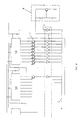
- The circuitry according to the invention is described in greater detail with reference to the accompanying Figure 3, in which, for applicable parts, the same reference numerals are used as in the systems described above.
- In the circuitry there are used transfer registers SR which have a series-form input and a parallel-form output. The inputs of the transfer registers are, in a known manner, a clock signal, the supply voltage, and the control data. According to the invention, a
phototransistor 1 and in series with it adiode 2 are coupled to each of the series-form outputs of the transfer registers. Thediodes 2 are all coupled to a common line c, which leads to the logic circuit. The transfer register SR gives in succession to each phototransistor 1 a voltage pulse, and the pulse frequency, i.e. the frequency between the adjacent phototransistors, is approx. 1 kHz. When a phototransistor receives voltage, it becomes conductive, and the signal received from the emitter is applied via thediode 2 to the common line c. If the connection between the phototransistor concerned and the diode at the same time transmitting infrared radiation is cut off by touching the panel, the effective signal due to modulation will be omitted from the emitter of the phototransistor and a modulation signal will not be switched to the common line c when the phototransistor is active. - For compensating for changes in the direct-voltage level of the line c it is possible to use, for example, the
compensation circuit 4 according to the Figure, the operation of which is described in greater detail in Patent Application FI 895243. - The circuitry according to the invention has advantages over the systems according to the state of the art. In the circuitry, the need for components is reduced, since no separate resistors and capacitors and no controllable switches are needed. The reduction of the number of components and wiring reduces the size of the circuit and increases its reliability.
Claims (2)
Applications Claiming Priority (2)
| Application Number | Priority Date | Filing Date | Title |
|---|---|---|---|
| FI895242A FI85543C (en) | 1989-11-03 | 1989-11-03 | Connection circuit for contact display panel |
| FI895242 | 1989-11-03 |
Publications (2)
| Publication Number | Publication Date |
|---|---|
| EP0426362A2 true EP0426362A2 (en) | 1991-05-08 |
| EP0426362A3 EP0426362A3 (en) | 1991-10-09 |
Family
ID=8529287
Family Applications (1)
| Application Number | Title | Priority Date | Filing Date |
|---|---|---|---|
| EP19900311638 Ceased EP0426362A3 (en) | 1989-11-03 | 1990-10-24 | Switching circuit for a contact display panel |
Country Status (3)
| Country | Link |
|---|---|
| US (1) | US5146081A (en) |
| EP (1) | EP0426362A3 (en) |
| FI (1) | FI85543C (en) |
Cited By (17)
| Publication number | Priority date | Publication date | Assignee | Title |
|---|---|---|---|---|
| US6947102B2 (en) | 2002-02-20 | 2005-09-20 | Plannar Systems, Inc. | Light sensitive display which senses decreases in light |
| US7023503B2 (en) | 2002-02-20 | 2006-04-04 | Planar Systems, Inc. | Image sensor with photosensitive thin film transistors |
| US7053967B2 (en) | 2002-05-23 | 2006-05-30 | Planar Systems, Inc. | Light sensitive display |
| US7773139B2 (en) | 2004-04-16 | 2010-08-10 | Apple Inc. | Image sensor with photosensitive thin film transistors |
| US8207946B2 (en) | 2003-02-20 | 2012-06-26 | Apple Inc. | Light sensitive display |
| US8441422B2 (en) | 2002-02-20 | 2013-05-14 | Apple Inc. | Light sensitive display with object detection calibration |
| US8638320B2 (en) | 2011-06-22 | 2014-01-28 | Apple Inc. | Stylus orientation detection |
| US8928635B2 (en) | 2011-06-22 | 2015-01-06 | Apple Inc. | Active stylus |
| US9176604B2 (en) | 2012-07-27 | 2015-11-03 | Apple Inc. | Stylus device |
| US9310923B2 (en) | 2010-12-03 | 2016-04-12 | Apple Inc. | Input device for touch sensitive devices |
| US9329703B2 (en) | 2011-06-22 | 2016-05-03 | Apple Inc. | Intelligent stylus |
| US9557845B2 (en) | 2012-07-27 | 2017-01-31 | Apple Inc. | Input device for and method of communication with capacitive devices through frequency variation |
| US9652090B2 (en) | 2012-07-27 | 2017-05-16 | Apple Inc. | Device for digital communication through capacitive coupling |
| US9939935B2 (en) | 2013-07-31 | 2018-04-10 | Apple Inc. | Scan engine for touch controller architecture |
| US10048775B2 (en) | 2013-03-14 | 2018-08-14 | Apple Inc. | Stylus detection and demodulation |
| US10061450B2 (en) | 2014-12-04 | 2018-08-28 | Apple Inc. | Coarse scan and targeted active mode scan for touch |
| US10474277B2 (en) | 2016-05-31 | 2019-11-12 | Apple Inc. | Position-based stylus communication |
Families Citing this family (8)
| Publication number | Priority date | Publication date | Assignee | Title |
|---|---|---|---|---|
| EP0567717B1 (en) * | 1992-04-30 | 2000-08-02 | REER S.p.A. | Optoelectronic barrier |
| JP2008523424A (en) * | 2004-12-09 | 2008-07-03 | アールピーオー プロプライエタリー リミテッド | Optical power distribution device |
| EP2338105B1 (en) | 2008-08-07 | 2012-12-19 | Owen Drumm | Optical control systems with modulated emitters |
| US9092092B2 (en) | 2008-08-07 | 2015-07-28 | Rapt Ip Limited | Detecting multitouch events in an optical touch-sensitive device using touch event templates |
| JP5378519B2 (en) * | 2008-08-07 | 2013-12-25 | ドラム,オウエン | Method and apparatus for detecting multi-touch events in optical touch sensitive devices |
| KR101548696B1 (en) * | 2008-08-07 | 2015-09-01 | 랩트 아이피 리미티드 | Optical control systems with feedback control |
| JP2010262555A (en) | 2009-05-11 | 2010-11-18 | Sony Corp | Information processing apparatus and method |
| US9524060B2 (en) | 2012-07-13 | 2016-12-20 | Rapt Ip Limited | Low power operation of an optical touch-sensitive device for detecting multitouch events |
Citations (2)
| Publication number | Priority date | Publication date | Assignee | Title |
|---|---|---|---|---|
| US3764813A (en) * | 1972-04-12 | 1973-10-09 | Bell Telephone Labor Inc | Coordinate detection system |
| US4703316A (en) * | 1984-10-18 | 1987-10-27 | Tektronix, Inc. | Touch panel input apparatus |
Family Cites Families (2)
| Publication number | Priority date | Publication date | Assignee | Title |
|---|---|---|---|---|
| JPS60207923A (en) * | 1984-03-31 | 1985-10-19 | Toshiba Corp | Position detector |
| US4893120A (en) * | 1986-11-26 | 1990-01-09 | Digital Electronics Corporation | Touch panel using modulated light |
-
1989
- 1989-11-03 FI FI895242A patent/FI85543C/en not_active IP Right Cessation
-
1990
- 1990-10-24 EP EP19900311638 patent/EP0426362A3/en not_active Ceased
- 1990-10-30 US US07/605,311 patent/US5146081A/en not_active Expired - Fee Related
Patent Citations (2)
| Publication number | Priority date | Publication date | Assignee | Title |
|---|---|---|---|---|
| US3764813A (en) * | 1972-04-12 | 1973-10-09 | Bell Telephone Labor Inc | Coordinate detection system |
| US4703316A (en) * | 1984-10-18 | 1987-10-27 | Tektronix, Inc. | Touch panel input apparatus |
Cited By (39)
| Publication number | Priority date | Publication date | Assignee | Title |
|---|---|---|---|---|
| US8441422B2 (en) | 2002-02-20 | 2013-05-14 | Apple Inc. | Light sensitive display with object detection calibration |
| US7023503B2 (en) | 2002-02-20 | 2006-04-04 | Planar Systems, Inc. | Image sensor with photosensitive thin film transistors |
| US6947102B2 (en) | 2002-02-20 | 2005-09-20 | Plannar Systems, Inc. | Light sensitive display which senses decreases in light |
| US9411470B2 (en) | 2002-02-20 | 2016-08-09 | Apple Inc. | Light sensitive display with multiple data set object detection |
| US9134851B2 (en) | 2002-02-20 | 2015-09-15 | Apple Inc. | Light sensitive display |
| US9971456B2 (en) | 2002-02-20 | 2018-05-15 | Apple Inc. | Light sensitive display with switchable detection modes for detecting a fingerprint |
| US7872641B2 (en) | 2002-02-20 | 2011-01-18 | Apple Inc. | Light sensitive display |
| US11073926B2 (en) | 2002-02-20 | 2021-07-27 | Apple Inc. | Light sensitive display |
| US8570449B2 (en) | 2002-02-20 | 2013-10-29 | Apple Inc. | Light sensitive display with pressure sensor |
| US7830461B2 (en) | 2002-05-23 | 2010-11-09 | Apple Inc. | Light sensitive display |
| US8044930B2 (en) | 2002-05-23 | 2011-10-25 | Apple Inc. | Light sensitive display |
| US7880733B2 (en) | 2002-05-23 | 2011-02-01 | Apple Inc. | Light sensitive display |
| US7880819B2 (en) | 2002-05-23 | 2011-02-01 | Apple Inc. | Light sensitive display |
| US7852417B2 (en) | 2002-05-23 | 2010-12-14 | Apple Inc. | Light sensitive display |
| US9354735B2 (en) | 2002-05-23 | 2016-05-31 | Apple Inc. | Light sensitive display |
| US7053967B2 (en) | 2002-05-23 | 2006-05-30 | Planar Systems, Inc. | Light sensitive display |
| US8207946B2 (en) | 2003-02-20 | 2012-06-26 | Apple Inc. | Light sensitive display |
| US8289429B2 (en) | 2004-04-16 | 2012-10-16 | Apple Inc. | Image sensor with photosensitive thin film transistors and dark current compensation |
| US7773139B2 (en) | 2004-04-16 | 2010-08-10 | Apple Inc. | Image sensor with photosensitive thin film transistors |
| US9310923B2 (en) | 2010-12-03 | 2016-04-12 | Apple Inc. | Input device for touch sensitive devices |
| US9921684B2 (en) | 2011-06-22 | 2018-03-20 | Apple Inc. | Intelligent stylus |
| US8638320B2 (en) | 2011-06-22 | 2014-01-28 | Apple Inc. | Stylus orientation detection |
| US9519361B2 (en) | 2011-06-22 | 2016-12-13 | Apple Inc. | Active stylus |
| US8928635B2 (en) | 2011-06-22 | 2015-01-06 | Apple Inc. | Active stylus |
| US9329703B2 (en) | 2011-06-22 | 2016-05-03 | Apple Inc. | Intelligent stylus |
| US9582105B2 (en) | 2012-07-27 | 2017-02-28 | Apple Inc. | Input device for touch sensitive devices |
| US9557845B2 (en) | 2012-07-27 | 2017-01-31 | Apple Inc. | Input device for and method of communication with capacitive devices through frequency variation |
| US9176604B2 (en) | 2012-07-27 | 2015-11-03 | Apple Inc. | Stylus device |
| US9652090B2 (en) | 2012-07-27 | 2017-05-16 | Apple Inc. | Device for digital communication through capacitive coupling |
| US10048775B2 (en) | 2013-03-14 | 2018-08-14 | Apple Inc. | Stylus detection and demodulation |
| US10845901B2 (en) | 2013-07-31 | 2020-11-24 | Apple Inc. | Touch controller architecture |
| US9939935B2 (en) | 2013-07-31 | 2018-04-10 | Apple Inc. | Scan engine for touch controller architecture |
| US11687192B2 (en) | 2013-07-31 | 2023-06-27 | Apple Inc. | Touch controller architecture |
| US10067580B2 (en) | 2013-07-31 | 2018-09-04 | Apple Inc. | Active stylus for use with touch controller architecture |
| US10067618B2 (en) | 2014-12-04 | 2018-09-04 | Apple Inc. | Coarse scan and targeted active mode scan for touch |
| US10664113B2 (en) | 2014-12-04 | 2020-05-26 | Apple Inc. | Coarse scan and targeted active mode scan for touch and stylus |
| US10061449B2 (en) | 2014-12-04 | 2018-08-28 | Apple Inc. | Coarse scan and targeted active mode scan for touch and stylus |
| US10061450B2 (en) | 2014-12-04 | 2018-08-28 | Apple Inc. | Coarse scan and targeted active mode scan for touch |
| US10474277B2 (en) | 2016-05-31 | 2019-11-12 | Apple Inc. | Position-based stylus communication |
Also Published As
| Publication number | Publication date |
|---|---|
| FI85543C (en) | 1992-04-27 |
| EP0426362A3 (en) | 1991-10-09 |
| FI895242A0 (en) | 1989-11-03 |
| US5146081A (en) | 1992-09-08 |
| FI85543B (en) | 1992-01-15 |
Similar Documents
| Publication | Publication Date | Title |
|---|---|---|
| EP0426362A2 (en) | Switching circuit for a contact display panel | |
| US4831359A (en) | Four quadrant touch pad | |
| US20040145575A1 (en) | Cross-point matrix for infrared touchscreen | |
| EP1204209A1 (en) | Capacitive touch sensor | |
| US4398181A (en) | Keyboard entry system | |
| ATE225528T1 (en) | METHOD FOR CONFIGURATION OF ELEVATOR CONTROLS | |
| US20030001223A1 (en) | Circuit layout for several sensor elements | |
| JPH0877894A (en) | Touch position detecting device | |
| US3444518A (en) | System for display and control of logic element outputs | |
| US4177409A (en) | Video amplifier for displaying four or more video levels on a cathode ray tube | |
| JP3021587B2 (en) | Key switch operation information capturing method and matrix key switch device | |
| US5936389A (en) | Terminating resistance circuit | |
| KR100481500B1 (en) | Micom Interface of an image signal receiver | |
| RU2013808C1 (en) | Device for collection, conversion and transmission of analog information | |
| CN114461094B (en) | Touch display panel and display device | |
| KR850001332Y1 (en) | Function selector switch circuit | |
| US3488523A (en) | L-network switching circuit | |
| JP2569635B2 (en) | Touch panel device | |
| US4287387A (en) | Teletypewriter loop switching matrix | |
| JP3104390B2 (en) | Switch device with touch panel | |
| KR940001509B1 (en) | Key matrix control circuit | |
| JPH0449715Y2 (en) | ||
| JPS6242288B2 (en) | ||
| JPH1021008A (en) | Optical touch switch device | |
| SU1285520A1 (en) | Information board |
Legal Events
| Date | Code | Title | Description |
|---|---|---|---|
| PUAI | Public reference made under article 153(3) epc to a published international application that has entered the european phase |
Free format text: ORIGINAL CODE: 0009012 |
|
| AK | Designated contracting states |
Kind code of ref document: A2 Designated state(s): AT BE CH DE DK ES FR GB GR IT LI LU NL SE |
|
| PUAL | Search report despatched |
Free format text: ORIGINAL CODE: 0009013 |
|
| AK | Designated contracting states |
Kind code of ref document: A3 Designated state(s): AT BE CH DE DK ES FR GB GR IT LI LU NL SE |
|
| 17P | Request for examination filed |
Effective date: 19920401 |
|
| 17Q | First examination report despatched |
Effective date: 19941122 |
|
| STAA | Information on the status of an ep patent application or granted ep patent |
Free format text: STATUS: THE APPLICATION HAS BEEN REFUSED |
|
| 18R | Application refused |
Effective date: 19950514 |