EP0419178A2 - Ink jet recording - Google Patents
Ink jet recording Download PDFInfo
- Publication number
- EP0419178A2 EP0419178A2 EP90310144A EP90310144A EP0419178A2 EP 0419178 A2 EP0419178 A2 EP 0419178A2 EP 90310144 A EP90310144 A EP 90310144A EP 90310144 A EP90310144 A EP 90310144A EP 0419178 A2 EP0419178 A2 EP 0419178A2
- Authority
- EP
- European Patent Office
- Prior art keywords
- ink
- temperature
- ink jet
- jet recording
- detecting
- Prior art date
- Legal status (The legal status is an assumption and is not a legal conclusion. Google has not performed a legal analysis and makes no representation as to the accuracy of the status listed.)
- Granted
Links
Images


Classifications
-
- B—PERFORMING OPERATIONS; TRANSPORTING
- B41—PRINTING; LINING MACHINES; TYPEWRITERS; STAMPS
- B41J—TYPEWRITERS; SELECTIVE PRINTING MECHANISMS, i.e. MECHANISMS PRINTING OTHERWISE THAN FROM A FORME; CORRECTION OF TYPOGRAPHICAL ERRORS
- B41J2/00—Typewriters or selective printing mechanisms characterised by the printing or marking process for which they are designed
- B41J2/005—Typewriters or selective printing mechanisms characterised by the printing or marking process for which they are designed characterised by bringing liquid or particles selectively into contact with a printing material
- B41J2/01—Ink jet
- B41J2/015—Ink jet characterised by the jet generation process
- B41J2/04—Ink jet characterised by the jet generation process generating single droplets or particles on demand
- B41J2/045—Ink jet characterised by the jet generation process generating single droplets or particles on demand by pressure, e.g. electromechanical transducers
- B41J2/04501—Control methods or devices therefor, e.g. driver circuits, control circuits
- B41J2/04541—Specific driving circuit
-
- B—PERFORMING OPERATIONS; TRANSPORTING
- B41—PRINTING; LINING MACHINES; TYPEWRITERS; STAMPS
- B41J—TYPEWRITERS; SELECTIVE PRINTING MECHANISMS, i.e. MECHANISMS PRINTING OTHERWISE THAN FROM A FORME; CORRECTION OF TYPOGRAPHICAL ERRORS
- B41J2/00—Typewriters or selective printing mechanisms characterised by the printing or marking process for which they are designed
- B41J2/005—Typewriters or selective printing mechanisms characterised by the printing or marking process for which they are designed characterised by bringing liquid or particles selectively into contact with a printing material
- B41J2/01—Ink jet
- B41J2/015—Ink jet characterised by the jet generation process
- B41J2/04—Ink jet characterised by the jet generation process generating single droplets or particles on demand
- B41J2/045—Ink jet characterised by the jet generation process generating single droplets or particles on demand by pressure, e.g. electromechanical transducers
- B41J2/04501—Control methods or devices therefor, e.g. driver circuits, control circuits
- B41J2/0455—Details of switching sections of circuit, e.g. transistors
-
- B—PERFORMING OPERATIONS; TRANSPORTING
- B41—PRINTING; LINING MACHINES; TYPEWRITERS; STAMPS
- B41J—TYPEWRITERS; SELECTIVE PRINTING MECHANISMS, i.e. MECHANISMS PRINTING OTHERWISE THAN FROM A FORME; CORRECTION OF TYPOGRAPHICAL ERRORS
- B41J2/00—Typewriters or selective printing mechanisms characterised by the printing or marking process for which they are designed
- B41J2/005—Typewriters or selective printing mechanisms characterised by the printing or marking process for which they are designed characterised by bringing liquid or particles selectively into contact with a printing material
- B41J2/01—Ink jet
- B41J2/015—Ink jet characterised by the jet generation process
- B41J2/04—Ink jet characterised by the jet generation process generating single droplets or particles on demand
- B41J2/045—Ink jet characterised by the jet generation process generating single droplets or particles on demand by pressure, e.g. electromechanical transducers
- B41J2/04501—Control methods or devices therefor, e.g. driver circuits, control circuits
- B41J2/04563—Control methods or devices therefor, e.g. driver circuits, control circuits detecting head temperature; Ink temperature
-
- B—PERFORMING OPERATIONS; TRANSPORTING
- B41—PRINTING; LINING MACHINES; TYPEWRITERS; STAMPS
- B41J—TYPEWRITERS; SELECTIVE PRINTING MECHANISMS, i.e. MECHANISMS PRINTING OTHERWISE THAN FROM A FORME; CORRECTION OF TYPOGRAPHICAL ERRORS
- B41J2/00—Typewriters or selective printing mechanisms characterised by the printing or marking process for which they are designed
- B41J2/005—Typewriters or selective printing mechanisms characterised by the printing or marking process for which they are designed characterised by bringing liquid or particles selectively into contact with a printing material
- B41J2/01—Ink jet
- B41J2/015—Ink jet characterised by the jet generation process
- B41J2/04—Ink jet characterised by the jet generation process generating single droplets or particles on demand
- B41J2/045—Ink jet characterised by the jet generation process generating single droplets or particles on demand by pressure, e.g. electromechanical transducers
- B41J2/04501—Control methods or devices therefor, e.g. driver circuits, control circuits
- B41J2/0458—Control methods or devices therefor, e.g. driver circuits, control circuits controlling heads based on heating elements forming bubbles
-
- B—PERFORMING OPERATIONS; TRANSPORTING
- B41—PRINTING; LINING MACHINES; TYPEWRITERS; STAMPS
- B41J—TYPEWRITERS; SELECTIVE PRINTING MECHANISMS, i.e. MECHANISMS PRINTING OTHERWISE THAN FROM A FORME; CORRECTION OF TYPOGRAPHICAL ERRORS
- B41J2/00—Typewriters or selective printing mechanisms characterised by the printing or marking process for which they are designed
- B41J2/005—Typewriters or selective printing mechanisms characterised by the printing or marking process for which they are designed characterised by bringing liquid or particles selectively into contact with a printing material
- B41J2/01—Ink jet
- B41J2/135—Nozzles
- B41J2/14—Structure thereof only for on-demand ink jet heads
- B41J2/14016—Structure of bubble jet print heads
- B41J2/14072—Electrical connections, e.g. details on electrodes, connecting the chip to the outside...
-
- B—PERFORMING OPERATIONS; TRANSPORTING
- B41—PRINTING; LINING MACHINES; TYPEWRITERS; STAMPS
- B41J—TYPEWRITERS; SELECTIVE PRINTING MECHANISMS, i.e. MECHANISMS PRINTING OTHERWISE THAN FROM A FORME; CORRECTION OF TYPOGRAPHICAL ERRORS
- B41J2/00—Typewriters or selective printing mechanisms characterised by the printing or marking process for which they are designed
- B41J2/005—Typewriters or selective printing mechanisms characterised by the printing or marking process for which they are designed characterised by bringing liquid or particles selectively into contact with a printing material
- B41J2/01—Ink jet
- B41J2/135—Nozzles
- B41J2/14—Structure thereof only for on-demand ink jet heads
- B41J2/14016—Structure of bubble jet print heads
- B41J2/14088—Structure of heating means
- B41J2/14112—Resistive element
- B41J2/14129—Layer structure
-
- B—PERFORMING OPERATIONS; TRANSPORTING
- B41—PRINTING; LINING MACHINES; TYPEWRITERS; STAMPS
- B41J—TYPEWRITERS; SELECTIVE PRINTING MECHANISMS, i.e. MECHANISMS PRINTING OTHERWISE THAN FROM A FORME; CORRECTION OF TYPOGRAPHICAL ERRORS
- B41J2/00—Typewriters or selective printing mechanisms characterised by the printing or marking process for which they are designed
- B41J2/005—Typewriters or selective printing mechanisms characterised by the printing or marking process for which they are designed characterised by bringing liquid or particles selectively into contact with a printing material
- B41J2/01—Ink jet
- B41J2/135—Nozzles
- B41J2/14—Structure thereof only for on-demand ink jet heads
- B41J2002/14379—Edge shooter
-
- B—PERFORMING OPERATIONS; TRANSPORTING
- B41—PRINTING; LINING MACHINES; TYPEWRITERS; STAMPS
- B41J—TYPEWRITERS; SELECTIVE PRINTING MECHANISMS, i.e. MECHANISMS PRINTING OTHERWISE THAN FROM A FORME; CORRECTION OF TYPOGRAPHICAL ERRORS
- B41J2202/00—Embodiments of or processes related to ink-jet or thermal heads
- B41J2202/01—Embodiments of or processes related to ink-jet heads
- B41J2202/13—Heads having an integrated circuit
Definitions
- the present invention relates to an ink jet recording head and an ink jet recording system having such head, which are used with a copying machine, facsimile, word processor, output printer of a host computer, video output printer and the like, and more particularly, it relates to an ink jet recording head and an ink jet recording system having such head, wherein electrical/thermal converting elements and functional elements are disposed on a common substrate.
- the present invention further relates to a temperature adjusting apparatus used with a recording system, and, more particularly, it relates to a temperature adjusting apparatus which includes a plurality of similar analogue sensors for detecting the surrounding condition (for example, temperature) and wherein the surrounding condition is measured by receiving the outputs from such sensors through an amplifying circuit to adjust the temperature of a recording head of the recording system.
- a temperature adjusting apparatus which includes a plurality of similar analogue sensors for detecting the surrounding condition (for example, temperature) and wherein the surrounding condition is measured by receiving the outputs from such sensors through an amplifying circuit to adjust the temperature of a recording head of the recording system.
- an ink jet recording system having a recording head wherein electrical/thermal converting elements and functional elements are arranged on the same substrate has been proposed, as disclosed for example in the Japanese Patent Laid-open No. 57-72867.
- the above-mentioned recording head is excellent, there is a room for further improving the recording head and the recording system to meet the requirements regarding the higher speed operation, less energy consumption, higher integration, cost-down and/or higher reliability strongly requested in the recent recording systems.
- a recording head having the high ability must be provided with a low cost.
- the recording is effected by discharging the liquid such as ink by the use of thermal energy generated from the electrical/thermal converting elements including heating resistive members.
- the temperature of the recording head is gradually increased as the recording operation is continued due to the fact that a part of the thermal energy generated is accumulated in the liquid and due to other reasons.
- the increase in the temperature of the recording head affects a bad influence upon the viscosity of ink, generation and growth of the bubble and the like, thus changing the amount of the discharged ink, and accordingly, the diameter of dots recorded on a recording medium. This results in the deterioration of the image quality, which should be avoided.
- a recording factor control for decreasing the temperature of the recording head on the basis of the detected temperature of the recording head for example, a control effected by stopping the recording operation or by using the Peltier element
- a temperature detecting element acting as a means for detecting the temperature of the recording head was provided for giving the output information for effecting such control.
- Fig. 1 illustrating a schematic perspective view of a recording head 10′.
- thermo/thermal converting elements are formed at an end of a semi-conductor substrate 51, and a top plate 52 including a liquid chamber therein is disposed on the substrate to define orifices 53.
- a temperature detecting portion is arranged on a mother board 54 at 60 or on the semi-conductor substrate 51 at 70. Concrete examples of the temperature detecting portion are shown in Figs. 2A and 2B.
- Fig. 2A shows an example that a thermistor 61 acting as a temperature sensor is mounted on the mother board 54.
- the disadvantage will arise regarding the number of parts, and thus, in the production line since the thermistor 61 must be added as a discrete element.
- Fig. 2B shows an example that a diode 71 having the P-N connection is formed on the semi-conductor substrate 51 made of single crystal silicon material by the semi-conductor process and a temperature sensor is provided by the use of the diode feature. That is to say, it is possible to achieve the higher functionality, higher integration and cost-down by forming the temperature sensor, by means of the semi-conductor process, on the substrate on which the electrical/thermal converting elements are disposed.
- the reference numeral 72 denotes an aluminium electrode
- 73 denotes an insulator layer made of SiO2.
- the recording heads can be manufactured in the same production line, dispersion in ink discharging features of the recording heads will occur.
- a method wherein the information corresponding to the electrical/thermal converting features of the electrical/thermal converting elements, and thus, the discharging feature is previously formed on the recording head, for example in the form of electric resistors, and the recording head is driven by determining the discharging signal as the recording factor on the basis of such information has been proposed.
- the electrical/thermal converting elements capable of generating the thermal energy enough to cause the change in the condition of ink and to discharge the ink from a discharge opening must be formed or provided.
- the functional elements for driving the recording head and for detecting the temperature of the head such as diodes, transistors and the like have the features depending upon the change in temperature (i.e., temperature dependence features), these must be activated under the temperature condition which is stable as long as possible.
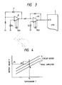
- Fig. 3 shows an example of a conventional measuring device for measuring the surrounding (environmental) condition such as for example a temperature.
- the reference numerals D denotes a diode acting as a temperature detecting sensor;
- A1, A2 denote amplifiers;
- C denotes a CPU forming a main portion of the measuring device.
- An object of the present invention is to solve the above-mentioned conventional drawbacks and to provide a recording head and a recording system having high ability, which can perform the recording at a high speed with high resolution stable for a long time.
- Another object of the present invention is to provide an inexpensive recording head wherein electrical/thermal converting elements and functional elements are disposed on the same substrate, and an inexpensive recording system having a temperature adjusting function of high ability.
- a further object of the present invention is to provide a recording system and a temperature adjusting apparatus which can perform the temperature adjustment properly without increasing the manufacturing cost and/or the dimension thereof and without lengthening the adjustment time, even if the number of the above-mentioned systems is increased.
- a still further object of the present invention is to provide an ink jet recording head comprising an ink discharging portion having a discharge opening for discharging ink; a substrate having an electrical/thermal converting element for generating thermal energy supplied to the ink discharging portion and used to discharge the ink, and a temperature detecting element; and an information bearing means for carrying information providing the feature of the temperature detecting element.
- the another object of the present invention is to provide an ink jet recording system comprising an ink jet recording head used for forming a desired image on a recording medium by discharging ink from a discharge opening in response to a predetermined input signal; a drive controlling means for controlling an operation of the ink jet recording head. It further comprises a temperature adjusting means having a detecting system including a detecting element for detecting the environmental condition surrounding the ink jet recording system, a memory means for storing an output value from the detecting system regarding an output of the detecting element as a reference or the result obtained by performing a predetermined calculation with respect to the output value, and a correcting means for correcting an error of the detecting system on the basis of the contents stored in the memory means.
- the pattern acting as the information bearing means for bearing or carrying the information providing the feature of the temperature detecting element is previously formed on the recording head, it is possible to correct the dispersion in the temperature detecting elements obtained by the semi-conductor process, with very simple method and arrangement, and to perform the proper temperature control.
- the data representing the characteristics of the circuit such as the value ⁇ V, V value at the point A and the like are stored in the memory means comprising an involatile memory and the correction of the measured values is effected on the basis of the contents stored in the memory.
- the error in the detecting system used is corrected on the basis of the contents stored in the memory means, when the control is effected in accordance with the environmental condition.
- Fig. 5A shows an equivalent circuit to the diode.
- a voltage reduction V F is created in a normal direction of the diode 71.
- the voltage reduction V F in the normal direction varies in response to the change in the temperature.
- the voltage reduction V F also varies in accordance with the density of current flowing in the diode. If the current is maintained at a constant value, the voltage reduction detected in the diode 71 in the normal direction will be determined only as a function of the temperature. That is to say, the relationship between the voltage reduction V F and the temperature will be expressed by the following equation (1): V F ⁇ KT/q ln (I F /I S ) (1) Where, K and q are constants called as "wave number" and "charge of electron", respectively. Further, I S is a given current constant derived from the area of the P-N connection, I F is a current value in the normal direction, and T is an absolute temperature.
- Fig. 5B is a graph showing the measurement result presenting the relationship given by the expression (2).
- V F is dispersed due to the dispersion derived from the diode production or manufacturing line.
- a recording head B manufactured in the same production line as a certain recording head A the dispersion of 30 mV will occur at a temperature of 25°C ( ⁇ T ). Converting this into the temperature, the detection error of 15°C will occur. If these two recording heads are used to be driven under the same condition, it will be impossible to detect the correct temperature, thus providing the insufficient power at the lower temperature, which causes the poor ink discharging and/or overheating the recording head due to the inadequate control at the higher temperature, which causes the deterioration of the image quality. Further, the service life of the recording heads will be shortened.
- the information bearing means for carrying the dispersion information of the diodes is disposed on a wiring substrate integrally fixed to a semi-conductor substrate on which the temperature detecting diode is arranged, the dispersion information inherent to the recording head is detected in a main body side, thereby permitting the correct temperature control.
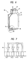
- Fig. 6 is a schematic perspective view of a recording head according to an embodiment of the present invention.
- the recording head 10 is constituted by a substrate 14 arranged on an aluminium base plate 11 and on which a temperature detecting sensor 13 is formed, a top plate 15 including a liquid chamber therein and disposed on the substrate, and a PCB plate 12 on which the wirings extending from the substrate 14 to an electric connector portion 16 are disposed. Further, on the PCB plate 12, a sensor rank detecting pattern 17 acting as an information bearing means is formed.
- the substrate 14 is electrically connected to the PCB plate 12 by a bonding wire and the like (not shown), and further, the plate is electrically connected to a main body of a printer through the electric connector portion 16 so that the head 10 is driven by a drive controlling circuit arranged in the main body side.
- Fig. 7 shows a portion of the sensor rank detecting pattern 17 of Fig. 6 in an enlarged scale.
- four pats 17-1, 17-2, 17-3 and 17-4 are used.
- Portions 18 to be bored correspond to three areas a , b and c encircled by broken line circles.
- the pat 17-4 is electrically earthed when the recording head is mounted on the recording system.
- the bearing means for carrying the ranking information is provided.
- electrically or optically reading the selectively opened or short-circuited pattern it is possible to rank the temperature sensor.
- the ranking for three bits i.e., the ranking into eight ranks will be fully explained.
- Fig. 8 is a schematic perspective view for explaining the substrate 14 of Fig. 6.
- the reference numeral 110 denotes electrical/thermal converting elements which are formed on a semi-conductor substrate 140 by a process which will be described later.
- the reference numeral 103 denotes heating resistive layers; and 104, 104′ denote a pair of electrodes.
- the reference numeral 120 denotes diodes acting as driving functional elements which are connected to the corresponding electrical/thermal converting element in series by the electrode 104 so that the current leakage is prevented when other electrical/thermal converting element is driven.
- the reference numeral 210 denotes diodes acting as temperature detecting functional elements (temperature sensors) which are arranged on both sides of the semi-conductor substrate 140 with the interposition of the electrical/thermal converting elements 110. These diodes are formed simultaneously with the formation of the driving diodes 120 by the process described later.
- the reference numeral 130 denotes heating members acting as functional elements (heating heaters) for heating the ink, which can perform the heating control by controlling the current supplied on the basis of the outputs from the temperature sensors 210. These heating heaters 130 are also arranged on both sides of the semi-conductor substrate 140.
- the reference numeral 160 denotes a wiring portion for the electrical/thermal converting elements, which is arranged between an array of the electrical/thermal converting elements 110 and an array of the driving diodes 120.
- the reference numerals 170 denote pats for providing the electric connection to the external equipments.
- Fig. 8 shows a portion of the substrate 14, an opposite portion of the substrate has a symmetrical arrangement.
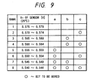
- the concrete ranking is shown in Fig. 9.
- the dispersion of the values V F is normally included in the following range: 0.540 ⁇ V F ⁇ 0.579 And, thus, there occurs the dispersion of about 40 mV. If the sensors are used as they are, there will arise the detection temperature error of about 20°C. However, by controlling the dispersion of the sensor diodes by means of this method and by discriminating the rank of the diodes, the dispersion thereof can be reduced to 1/8 of the original dispersion, and thus, it is possible to suppress the dispersion within a range of about 2.2°C.
- Fig. 10 shows a reading circuit arranged in the main body side of the recording system when the head so ranked is used.
- the pat 17-4 is earthed.
- the three pats 17-1, 17-2 and 17-3 are used to detect the rank of the sensor.
- the ranking pattern portions connected to the pats 17-2 and 17-3 are bored, thus forming the open circuits regarding the pats 17-2 and 17-3.
- the pattern portion connected to the pat 17-1 is not bored or cut so that the voltage in this pat is maintained at the earth voltage.
- the head having the so cut pattern By comparing the head having the so cut pattern with a corresponding table such as shown in Fig. 9, it can be judged that the head is included in the rank 4 (i.e., the sensor has the dispersion of 0.560 to 0.565 at a room temperature).
- the recording factor setting means reads the rank of the head whenever a power source of the main body of the recording system is turned ON, and three-bit information read is stored in a RAM in place.
- the three-bit information stored in the RAM can be read by the CPU.
- the current value to be supplied is determined, and such current is supplied to the heating heaters 130.
- Fig. 13 is a schematic view of a recording system for explaining the above-mentioned control system, where the reference numeral P denotes a platen for feeding a recording medium; CU denotes a control circuit including a sensor rank judging circuit, record factor setting circuit, heat signal generating circuit, drive signal generating circuit, carriage driving circuit and CPU; and H denotes a head having an ink tank and removably mounted on the recording system.
- the ink discharging electrical/thermal converting elements 110 may be energized at a level which does not discharge the ink.
- both the heating heater 130 and the electrical/thermal converting elements 110 may be used altogether.
- the controls of these elements are effected through a heat signal from the heat signal generating circuit on the basis of the parameters set by the record factor setting circuit. Further, when the driving condition for the ink discharge is changed, such change is effected through a drive signal from the drive signal generating circuit under the same process.
- the ranking is not limited to this three-bit into eight ranks, but may comprise four-bit into 16 ranks, five-bit into 32 ranks, two-bit into four ranks or the like, in accordance with the degree of the dispersion.
- the dispersion of the voltage reduction V F in the normal direction of the temperature sensors comprising the diodes integrally formed on the head can be judged by ranking the sensors, it is possible to perform the fine and correct control according to the dispersion. Further, since the pattern portions on the PCB plate are merely cut, the setting can be done easily and the image quality can be improved.
- Fig. 11 is a schematic sectional view of the substrate 14 taken along the line A-A′ of Fig. 8.
- the reference numeral 200 denotes a P-type semi-conductor plate made of a single crystal silicone material; 201 denotes an N-type semi-conductor embedded layer; 202 and 202′ denote P-type semi-conductor separating areas; 203 denotes an N-type semi-conductor epitaxial growth area; 204 denotes a P-type semi-conductor base area; and 205 denotes an N-type semi-conductor emitter area.
- the collector area is constituted by the N-type semi-conductor areas 203′, 201 and 206.
- Base-collector common electrodes 301 made of aluminium material and electrodes 302 are electrically connected through ohmic contact areas 207, 208 and 209 of high impurity density material.
- the process for forming the electrical/thermal converting elements on the substrate is added. This process includes a step of electrically connecting between the electrical/thermal converting elements and the functional elements.
- an N-P-N transistor is formed, and the areas 206, 208 completely enclose the emitter area 205 and the base area 204. Further, each cell is electrically isolated by the element separating areas enclosing these areas and the separating areas 202, 202′.
- a heat accumulating layer 102 comprising an SiO2 film is formed, by a PCVD method or a spattering method, on a heat-oxidized SiO2 film 101 on the substrate having the above-mentioned driving portions, and thereon, the electrical/thermal converting elements comprising an HfB2 heat resistance layer 103 obtained by the spattering method and aluminium electrodes 104, 104′ obtained by the spattering method are formed. Further, on the heating portions 110 of the electrical/thermal converting elements, an SiO2 protection film 105 obtained by the spattering method, and a Ta protection film 106 for preventing the cabitation are formed.
- the SiO2 film forming the heat accumulation layer 102 is formed integrally with insulation films between the wirings 301, 302 and 303.
- the transistor having the short-circuited base and collector as shown in Figs. 6 and 7, since the building-up feature thereof is excellent and the parasitic effect is relatively low, the dispersion between the elements can be further reduced. Further, by earthing the isolation electrodes 302, it is possible to prevent the electric charge from flowing into the adjacent cell, thus preventing the erroneous operation of the other elements.
- the recording head is completed by attaching the top plate made of glass or resin material and adapted to constitute the ink discharging portion having the ink discharge opening for discharging for example the ink, to the substrate having the electrical/thermal converting elements and the functional elements operated as mentioned above.
- HfB2 material is coated by a thickness of about 1000A to form the heat resistance layer 103.
- Aluminium layer is coated on this layer 103 and is patterned to simultaneously form the pair of electrodes 104, 104′ of the electrical/thermal converting elements, anode electrode wiring (not shown) and cathode wiring (not shown) of the diodes, and the electric connections therefor.
- the SiO2 layer 105 acting as the protection layer for the electrical/thermal converting elements and the insulation layers between the aluminium layer wirings is deposited by the spattering method, and Ta material is deposited on the heating portions of the electrical/thermal converting elements by a thickness of about 2000 ⁇ to form the anti-cabitation protection layer 106.
- the substrate as shown in Fig. 6 is obtained.
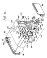
- the ink jet cartridge IJC in this embodiment has a large ink containing ability and has a configuration that the front end of the ink jet unit IJU is slightly protruded beyond the front face of the ink tank IT.
- the ink jet cartridge IJC can be fixedly supported by a positioning means and electrical contacts (described later) of the carriage HC (Fig. 17) mounted on the ink jet recording system IJRA and is of non-returnable or disposable type which can removably mounted on the carriage HC.
- the ink jet unit IJU is a bubble jet type unit which performs the recording by utilizing the electrical/thermal converting elements for generating thermal energy adapted to create the film boiling into the ink in response to an electric signal.
- the reference numeral 14 denotes a heater board on which a plurality of rows of electrical/thermal converting elements (discharging heaters) disposed on an Si substrate and aluminium electrical wiring for supplying the electric power to the elements are formed by the film forming technique.
- the reference numeral 12 denotes a wiring substrate corresponding to the heater board 14 and including wirings corresponding to those of the heater board 14 (which are connected to each other by the wire bonding) and pats 12-1 arranged at the ends of the wirings for receiving the electric signals from the recording system.
- the reference numeral 1300 denotes a top plate with recesses having partition walls for separating a plurality of ink passages independently and a common liquid chamber, which top plate integrally includes an ink receiving port 1500 for receiving the ink supplied from the ink tank and for introducing the ink into the common liquid chamber, and an orifice plate 400 having a plurality of ink discharge openings. While material of the top plate is preferably polysulfone, but other moulding resin material may be used.
- the reference numeral 11 denotes a support (for example made of metal) for flatly supporting the back surface of the wiring substrate 12, which support 11 forms a bottom plate of the ink jet unit.
- the reference numeral 500 denotes an M-shaped leaf spring which urges the common liquid chamber at its central portion and urges a portion of the liquid passages with a line contact by a front bent portion 501 formed on the spring.
- the heater board 14 and the top plate 1300 are engaged by each other by engaging a foot of the leaf spring 500 extending through a hole 3121 of the support 11 with the back surface of the support 11, and the heater board 14 is firmly fixed to the top plate 1300 by the biasing force of the leaf spring 500 and its front bent portion 501.
- the support 11 has positioning holes 312, 1900, 2000 engaged by two positioning projections 1012 and positioning and heat fusing retaining projections 1800, 1801 formed on the ink tank IT and is further provided at its back surface with positioning projections 2500, 2600 for the carriage HC of the ink jet recording system IJRA.
- the support 11 has a hole 320 through which an ink supply tube 2200 (described later) for permitting the ink supply from the ink tank.
- the wiring substrate 12 is attached to the support 11 by an adhesive.
- recesses 2400 are formed in the support 11 near the positioning projections 2500, 2600, respectively, and are positioned so that, when the ink jet cartridge IJC is assembled (see Fig. 15), the recesses are situated on the extension points of a head front area constituted by a plurality of parallei grooves 3000, 3001 at three sides of the head, thus preventing the foreign matters such as dust, ink and the like from reaching the positioning projections 2500, 2600.
- a lid member 800 having the parallel grooves 3000 forms an outer wall of the ink jet cartridge IJC and defines a space for receiving the ink jet unit IJU.
- an ink supply member 600 having the parallel grooves 3001 has an ink supply conduit 1600 communicating with the ink supply tube 2200, which ink supply conduit is fixedly supported at the ink supply tube 2200 side in a cantilever fashion.
- a seal pin 602 is inserted.
- the reference numeral 601 denotes a packing for providing a connection seal between the ink tank IT and the ink supply tube 2200; and 700 denotes a filter disposed at an end of the ink supply tube near the ink tank.
- the ink supply member 600 Since the ink supply member 600 is formed in the moulding operation, it can be manufactured at low cost and with high accuracy, and, even when the ink jet units are manufactured in the mass-production, the cantilevered ink supply conduit 1600 of the ink supply member can stably be pressed against the ink receiving port 1500. In the illustrated embodiment, the perfect communication can be positively obtained merely by applying any sealing adhesive to the pressed contacting portion between the port 1500 and the conduit 1600 from the ink supply member side.
- the ink supply member 600 is fixedly attached to the support 11 by protruding pins (not shown) formed on the back surface of the ink supply member 600 through holes 1901, 1902 formed in the support 11 and then by fusing the protruded ends of the pins onto the back surface of the support 11 by heat. Since such heat-fused and slightly protruded portions on the back side of the support 11 can be received in recesses (not shown) formed in a surface of the ink tank IT to which the ink jet unit IJU are to be attached, the ink jet unit IJU can be correctly positioned.
- the ink tank comprises a cartridge body 1000, an ink absorber 900, and a lid member 1100 for sealingly closing the cartridge body 1000 after the ink absorber 900 is inserted into the cartridge body from a side opposite to the side to which the unit IJU is attached.
- the ink absorber 900 is arranged in the cartridge body 1000 for holding the ink therein.
- the reference numeral 1200 denotes a supply port for supplying the ink to the unit ICU comprising the above-mentioned elements 100 - 600.
- This port 1200 also serves as a pouring port for impregnating the ink into the ink absorber 900 by pouring the ink from this port before the ink jet unit IJU is installed on a portion 1010 of the cartridge body 1000.
- the portion through which the ink can be supplied include an atmosphere vent opening 1401 and this supply port 1200.
- an air existing space or area in the tank defined by ribs 2300 of the cartridge body 1000 and partial ribs 2301, 2302 of the lid member 1100 is communicated with the atmosphere vent opening 1401 and is formed in a corner area remote from the supply port 1200.
- the relatively good and uniform supply of the ink to the ink absorber can be effected through the supply port 1200. This is very effective in a practical use.
- the ribs 2300 comprise four ribs arranged on the surface of the cartridge body 1000 at its rear portion and extending parallel to a carriage moving direction, so that the ink absorber is prevented from being closely contacted with the rear surface.
- the partial ribs 2301, 2302 are formed on the inner surface of the lid member 1100 on extension lines of the ribs 2300, but, unlike to the ribs 2300, the partial ribs are divided into plural pieces to more increase the air existing space than the ribs 2300.
- the partial ribs 2301, 2302 are distributed on an area smaller than a half of the whole surface area of the lid member 1100.
- the reference numeral 1401 denotes the aforementioned atmosphere vent opening formed in the lid member for communicating the interior of the cartridge with the atmosphere; and 1400 denotes a liquid anti-flow member arranged in the atmosphere vent opening 1400 for preventing the ink from leaking through the opening 1401.
- the ink containing space in the ink tank IT has a parallelepipedal shape, and the longer side surfaces thereof correspond to the side wall of the tank.
- the above-mentioned rib arrangement is particularly effective.
- the longer side surfaces are parallel to the carriage moving direction or the ink containing space has a cubic shape, the ink supply from the ink absorber 900 can be stabilized by arranging the ribs on the whole surface of the lid 1100.
- each positioning projection 1012 adapted to be engaged by the positioning holes 312 formed in the support 11 are disposed on this straight line L1.
- the height of each positioning projection 1012 is slightly smaller than a thickness of the support 11, these projections being used to position the support 11.
- a pawl 2100 adapted to be engaged by an engagement surface 4002 of a bent portion of a carriage positioning hook 4001, so that the force for positioning the carriage acts in a surface area parallel to the above-mentioned reference face including the straight line L1 (Fig. 17).
- Such relationship is effective since the positioning accuracy for only the ink tank equals to the positioning accuracy for the discharge openings of the head (The details will be described later with reference to Fig. 17).
- projections 1800, 1801 of the ink tank corresponding to holes 1900, 2000 of the support 11 are longer than the aforementioned projections 1012, so that the portions of the projections protruded from the support 11 can be fused by heat to be fixed to the surface of the support.
- a curve shown by L4 indicates a position of an outer wall of the ink supply member 600 when installed. Since the projections 1800, 1801 are situated along the curve L4, the sufficient strength and positional accuracy are provided by these projections, regardless of the weight of the front end portion of the head IJH.
- the reference numeral 2700 denotes a front tab of the ink tank IT adapted to be inserted into a hole formed in a front plate 4000 of the carriage.
- the reference numeral 2101 denotes an engagement tab for engaging by a further engagement portion of the carriage HC.
- the ink jet unit IJU Since the ink tank IT is covered by a lid or cap 800 after the ink jet unit IJU is mounted on the ink tank, the ink jet unit IJU is enclosed except its lower opening. However, in the ink jet cartridge IJC, since the lower opening thereof is situated closely adjacent to the carriage HC when it is mounted on the carriage, the ink jet cartridge will be enclosed substantially at all sides thereof. Thus, the heat generated from the ink jet head IJH disposed in this enclosed space is effective to maintain a certain temperature in this space. However, when the recording system is continuously operated for a long time, the temperature in this space is increased.
- a slit 1700 having a width smaller than that of the aforementioned space is formed in the upper surface of the cartridge IJC so that the increase in temperature in the space is prevented and the uniformity of the temperature distribution in the whole ink jet unit IJU is maintained regardless of the change in the environmental condition.
- the ink jet cartridge IJC When the ink jet cartridge IJC is assembled, the ink is supplied to the supply tank 600 through the supply port 1200, hole 320 formed in the support 11 and an introduction opening formed in the back surface of the supply tank 600 at its central position. After flowing in the supply tank, the ink then flows into the common liquid chamber through an outlet opening formed in the tank, an appropriate supply tube and an ink introduction opening 1500 of the top plate 1300. At conjunction portion in such ink flowing path, any packings made of, for example, silicone rubber, butyl rubber and the like are arranged to ensure the sealing thereof and to keep the ink flowing path without leakage.
- the top plate 1300 is made of resin material having the good anti-ink property (not deteriorated by the ink) such as polysulfone, polyethersulfone, polyphenylene oxide, polypropylene and the like, and is moulded integrally with the orifice plate 400 in a mould simultaneously.
- resin material having the good anti-ink property such as polysulfone, polyethersulfone, polyphenylene oxide, polypropylene and the like
- the ink supply member 600, top plate 1300 and orifice plate 400, and the ink tank body 1000 are formed as integral parts, respectively, the assembling accuracy is increased and the quality of the product is also improved even if it is manufactured in the mass-production line. Further, since the number of parts is reduced in comparison with the conventional manufacturing process, it is possible to obtain the desired features positively and easily.
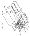
- the reference numeral 5000 denotes a platen roller for guiding a recording medium from downward to upward.
- the carriage HC can be shifted along the platen roller 5000.
- the front plate 4000 (having a thickness of 2 mm) disposed on the front side of the ink jet cartridge IJC, an electric connection portion supporting plate 4003 for holding a flexible sheet 4005 provided with pats 2001 corresponding to the pats 12-1 of the wiring substrate 12 of the cartridge IJC and a rubber pad 4006 for generating an elastic force for urging the flexible sheet from its back in coincidence with the pats 2011, and a positioning hook 4001 for fixing the ink jet cartridge IJC in a recording position are arranged.
- the front plate 4000 has a positioning projecting surfaces 4010 in correspondence with the aforementioned positioning projections 2500, 2600 of the support 11 of the cartridge, and is subjected to a vertical force directing toward the projecting surfaces 4010 after the carriage is mounted.
- a plurality of reinforcement ribs are provided in the direction of the vertical force. These ribs also form a head protection protruding portion protruding toward the platen roller slightly (about 0.1 mm) from a front surface position L5 when the cartridge is mounted.
- the electric connection portion supporting plate 4003 has a plurality of reinforcement ribs 4004 in a direction perpendicular to the aforementioned ribs and the degree of the projection of these ribs 4004 is gradually decreased from the platen roller to the hook 4001.
- the supporting plate 4003 has a positioning face 4008 facing the platen roller, and a positioning face 4007 facing the hook to stabilize the electrical contact condition. Between these faces, a pat contact area is formed, and the supporting plate defines an amount of the deformation of a ridge rubber sheet 4006 corresponding to the pat 2011.
- the pats 12-1 of the wiring substrate 12 are arranged symmetrically with respect to the aforementioned straight line L1, the amounts of the deformation of the ridges of the rubber sheet 4006 are uniformed to more stabilize the contacting pressure between the pats 2011 and 12-1.
- the pats 12-1 are arranged in two upper and lower rows and in two lines.
- Fig. 14 while the pats 12-1 were merely schematically shown for illustrating the other construction with detail, it should be noted that these pats 12-1 have the aforementioned ranking pats 17 and the pats 2011 have a corresponding construction for reading the ranking pats.
- the hook 4001 has a slot engaged by a fixed shaft 4009. By using the lost motion of the slot, after the hook is rotated in an anti-clockwise direction from a position shown in Fig. 17, by shifting the hook in the left direction along the platen roller 5000, the ink jet cartridge IJC can be positioned with respect to the carriage HC. While the hook 4001 can be shifted in any manner, but preferably the movement of the hook is effected by a lever arrangement and the like. In any case, during the rotation of the hook 4001, while the cartridge IJC is shifted toward the platen roller, the positioning projections 2500, 2600 are shifted to a position where they can be abutted against the positioning faces 4010.
- the engagement surface 4002 of the bent portion of the hook engages by the pawl 2100 of the cartridge IJC. Then, by rotating the cartridge IJC in a horizontal plane around the contacting area between the positioning faces 2500 and 4010, the pats 12-1 are eventually contacted with the pats 2011. And, when the hook 4001 is held in a predetermined position or fixed position, the perfect contact between the pats 12-1 and 2011, the perfect contact between the positioning faces 2500 and 4010, the contact between the engagement surface 4002 and the pawl 2100, and the contact between the wiring substrate 12 and the positioning surfaces 4007, 4008 are simultaneously attained, thus completing the holding of the cartridge IJC with respect to the carriage.
- Fig. 18 schematically shows an ink jet recording system embodying the present invention.
- the carriage HC has a pin (not shown) engaged by a spiral groove 5004 formed in a lead screw 5005 rotated through driving force transmitting gears 5011, 5009 in response to the normal rotation of a driving motor 5013, so that the carriage can be reciprocably shifted in directions shown by the arrows a and b.
- a sheet holder 5002 urges a sheet (recording medium) against the platen roller 5000 through the moving direction of the carriage.
- Home position detecting means 5007, 5008 detect the presence of a lever 5006 of the carriage by their photo couplers to control the switching of the rotational direction of the driving motor 5013.
- a supporting member 5016 supports a cap member 5022 covering the front surface of the recording head, and an absorbing means 5015 performs the absorbing recovery of the recording head through an opening 5023 formed in the cap member.
- a support member 5019 supports a cleaning blade 5017 for movement in a fore and aft direction, and these are supported by a support plate 5018 of the body. It should be noted that the cleaning blade is not limited to the illustrated configuration, but may be any conventional one.
- a lever 5021 for initiating the suction for the absorbing recovery is shifted in synchronous with the movement of a cam 5020 engaged by the carriage, and the movement of the lever can be controlled by the driving force from the driving motor through a conventional transmitting means such as a clutch and the like.
- Fig. 13 An example of the most characteristic circuit among these drive control systems was shown in Fig. 13. Now, the relationship between Fig. 13 and Fig. 10 will be described.
- the sensor rank judging circuit reads out the rank data on a data line electrically connected to the pats 17-1, 17-2 and 17-3 on the basis of the timing controlled by the CPU through a noise preventing shumit circuit (not shown).
- the resistors shown in Fig. 10 are pull-up resistors which can keep the line voltage at a constant value (for example, + 5 volts) when the line of the pat is opened.
- Fig. 19 shows an example of a color ink jet recording system of a so-called bubble jet type having the electrical/thermal converting elements as an energy generating means, embodying the present invention.
- a recording medium 401 such as a paper or a plastic sheet is supported by two pair of feeding rollers 402, 403 arranged on both upper and lower sides of a recording area, and is fed in a direction shown by the arrow A by means of the feeding rollers 402 driven by a sheet feeding motor 404.
- Ahead of the feeding rollers 402, 403, a guide shaft 405 is arranged in parallel to these rollers.
- a carriage 406 is shifted along the guide shaft 405 by the output of a carriage motor 407 through a wire 408 in a direction shown by the arrow B.
- An ink jet recording head unit 490 of bubble jet type is mounted on the carriage 406.
- the recording head unit 490 can form a color image and is arranged in a scanning direction, and includes four recording heads 409A, 409B, 409C and 409D corresponding to cyan (C) ink, magenta (M) ink, yellow (Y) ink and black (BK) ink, respectively.
- a plurality of ink discharge openings 410 arranged in a vertical direction at a predetermined interval are formed on the surface facing the recording medium 401.
- the electrical/thermal converting element (heat resistor and the like) 411 associated with each discharge opening 410 an ink droplet is flying from the corresponding discharge opening due to the pressure created by the bubble.
- a desired recording is effected.
- a circuit substrate of a driving circuit (driver) 429 for performing the driving as mentioned above is mounted on each recording head 409.
- a control portion including a control circuit (CPU), ROM and RAM provided in the CPU and the like is formed on a control substrate 415, and this control portion receives a command signal and a data signal from a host device 414 such as a computer and applies the driving voltage (heat voltage) of the electrical/thermal converting element to each recording head 409A - 409D through a heat driver 413 and driving sources for various motors, on the basis of the received signal.
- a control circuit CPU
- ROM and RAM provided in the CPU and the like
- An operation panel 560 attached to an outer casing (not shown) of the recording system comprises a key setting portion including an on-line/off-line changing key 416A, a line feed key 416B, a form feed key 416C, and a record mode changing key 416D, and a display portion including a plurality of alarm lamps 416E and a warning lamp 416F such as a power source lamp.
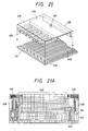
- FIG. 20 shows an example of a head chip arranged in each recording head according to this embodiment.
- a heater board 441 comprises a silicone substrate on which electrical/thermal converting elements (discharging heaters) 445 and aluminium wirings 446 for supplying electric power to the discharging heaters are formed by the film forming technique.
- the head chip is completed by adhering a top plate 430 having partition walls for defining recording liquid passages 425 to the heater board 441.
- the recording liquid (ink) is supplied to a common liquid chamber 423 through a supply port 424 formed in the top plate 430, and then is introduced into each nozzle 425.
- the heater 445 is heated by energizing it, the bubble is created in the ink filled in the nozzle 425, thereby discharging the ink droplet from the discharge opening 426.
- Figs. 21A and 21B are a plan view and an enlarged view of the heater board according to this embodiment.
- the reference numeral 443 denotes a discharging heater portion. Terminals 444 are connected to any external equipments through the wire bonding. Temperature sensors 442 acting as temperature detecting means are formed on the discharging heater portion 443 by the film forming technique as same as that used in the formation of the discharging heater portion.
- Fig. 21B shows a portion B including the sensor 442 of Fig. 21A in an enlarged scale.
- the reference numeral 448 denotes a lagging or heat keeping heater acting as a heating means.
- the sensors 442 are formed by the film forming technique like to other elements, they have the very high accuracy, and they can be made of material having the conductivity varying in accordance with the temperature, such as aluminium, titanium, tantalum, tantalum pentoxide, niobium and the like.
- aluminium is a material which can be used to form the electrodes
- titanium is a material which can be disposed between the heat resistance layer constituting the electrical/thermal converting element and the electrode to enhance the adhesion ability therebetween
- tantalum is a material which can be disposed on the protection layer on the heat resistance layer to enhance the anti-cabitation ability of the protection layer.
- the width of the wiring is increased, and, in order to reduce the influence from the wiring resistance, the wirings are arranged in a zigzag fashion, thereby providing the high resistance.
- the senor 442 may be constituted by a diode to effectively utilize the feature of the diode that the voltage in the normal direction of the diode (i.e., diode forward voltage) is changed in response to the temperature.
- Fig. 21C shows the temperature feature of the diode.
- the heat keeping heater 448 can be made of material (for example, HfB2) same as that of the heat resistance layer of the discharging heater 405, but may be made of other material constituting the heater board, such as aluminium, tantalum, titanium and the like.
- the temperature sensors 442 are arranged on both sides of the heater board 441, the temperature distribution on the substrate in the direction of the array of the nozzles 425 can be known from the outputs of the temperature sensors. Further, since the heat keeping heaters 448 are arranged in the vicinity of the temperature sensors 442, the temperature detection is swiftly responsive to the change in temperature due to the heating. By using this feature, the control for keeping the temperature distribution on the substrate at a given value can be performed with high response and high stability.
- Fig. 22 schematically shows a control system for the ink jet recording system of Fig. 19.
- the reference numeral 415A denotes a record controlling portion disposed on the control substrate 415 and adapted to perform the recording operation while effecting the control for various portions of the recording system; and 415B denotes an interface portion for sending and receiving various signals between it and the outside host device.
- the record controlling portion 415A may be in the form of a microcomputer comprising a CPU for performing the control operation, a ROM storing a program including the control sequence, a RAM having a recording data developing area and a working area, and the like.
- a central portion of an environmental condition measuring apparatus (described later with reference to Fig. 23) is integrally incorporated in the recording system.
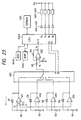
- Fig. 23 shows an example that a temperature adjusting apparatus is integrally incorporated into the record controlling portion.
- the reference numerals D1 - D4 denote temperature sensors 402 (in this example, diodes) disposed on the recording heads 409A - 409D; 451 denotes amplifiers each having a constant current circuit; 452 denotes an analogue switch which can select one of the outputs of the amplifiers 451 on the basis of control signals A, B; and 453 denotes an amplifier for receiving the output of the analogue switch.
- the reference numeral 454A denotes a CPU constituting a main controlling portion of the recording system according to this example and adapted to perform the correction data storing operation and the measuring operation in accordance with a predetermined sequence which will be described later with reference to Figs. 24 and 26; 454B denotes a ROM for storing the program including such sequence and other given data; and 454C denotes a RAM having a data developing area and a working area.
- the reference numeral 455 denotes a non-volatile memory, for example, in the form of EEPROM; 460 - 463 denote heat keeping heaters (448) arranged on the heater boards of the recording heads 409A - 409D; and 456 - 459 denote drivers for the heat keeping heaters.
- the diodes are used as the temperature sensors, and the temperature is detected by the use of the temperature feature of the diode forward voltage reduction V F .
- the output selected by the analogue switch 452 on the basis of the control signals A, B is compared with the reference voltage in the amplifier 453, and the voltage difference is multiplied by R6/R5 to obtain the output of the amplifier 453.
- the output V0 is a function of the voltage V F of the temperature sensor.
- the amplifiers 451, 453 are not ideal amplifiers and include input offset voltages and the like, and thus, the influence of these amplifiers upon the final output V0 cannot be negligible.
- the output V0 is influenced upon the offset voltages V1, V2.
- Fig. 23 since the analogue
- the following method is adopted for correcting the output V0 of the amplifier to detect the correct temperature.
- Fig. 24 shows an example of the procedure for obtaining the correction data, which correction can be carried out at the manufacturing stage or maintenance stage of the recording system.
- Fig. 26 shows an example of the head temperature controlling procedure for the recording head of Fig. 23.
- the channel of the analogue switch 452 is designated by an output 01 or 02 (step S11). Then, the output value Vu regarding the selected recording head is A/D-converted (step S13), and then, by using this value V0 and the constant C1 previously stored in the non-volatile memory 455, (V0 - C1) is calculated (step S15). Next, on the basis of this result (V0 - C1), the temperature T is calculated in accordance with the relation shown in Fig. 25 or is sought by referring to the table (step S17).
- the heat keeping heaters i.e., temperature maintaining heaters
- the heat keeping heaters i.e., temperature maintaining heaters
- step S21, S23 the heat keeping heaters in each recording head are ON/OFF controlled.
- V F ′(T) is, for example, a temperature feature of the diode having the feature as shown by the line b in Fig. 27.
- the difference between the line b and the line a is constant through all of the temperature range.
- a means for judging or discriminating the V F feature inherent to the diode is also provided in each recording head.
- Such means may include an additional non-volatile memory arranged in the recording head, which can store the necessary information and from which the information can read out at need.
- a pattern capable of having the judging information of a few bits is formed on the heater board, and, when the dispersion in the features of the diode sensors is checked, two-bit information may be obtained by cutting or short-circuiting the pattern of the recording head side.
- V0 V0′ - A ⁇ V F ′(T) - V F (T) ⁇ (9) is calculated, and the value V0′ can correspond to the value V0 in the case of the standard feature.
- the temperature T is sought by utilizing the relation shown in Fig. 25, and the proper head temperature control can be performed.
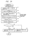
- Fig. 29 shows a control sequence in this third embodiment.
- a process for classifying and judging the sensor information step S14A
- a process for calculating the value V0 on the basis of such information and the circuit feature step S14B
- resistor sensors 442 shown in Figs. 21A and 21B are used as the temperature sensors will be described.
- the resistor sensor has a feature that the resistance value thereof increases as the temperature is increased. Also in this case, as in the case of the diode, there arises the dispersion in the features.
- the constant C1 inherent to the circuit is calculated by using the reference resistance R0 as a reference value for this sensor and by A/D converting the value V0 at that time, and the calculated value C1 is stored in the non-volatile memory 455.
- the environmental condition may be, for example, a humidity affecting an influence upon the viscosity of the ink.
- humidity sensors may be used, but the other elements are the same as those shown in Fig. 23.
- the temperature control can be performed in the same manner as described above. Further, various kinds of sensors may be used in combination.
- the present invention when the present invention is applied to the ink jet recording system, the present invention gives the excellent advantages, particularly, in the bubble jet recording head and bubble jet recording system, for the reason that, since the thermal energy is used as an energy for effecting the recording in the bubble jet recording system, the control can be performed in response to the environmental condition (temperature) in consideration of the heat of the recording system.
- the typical construction and principle thereof can be realized by using the fundamental principles, for example, disclosed in U.S. Patent Nos. 4,723,129 and 4,740,796.
- this system can be applied to both a so-called “on-demand type” and “continuous type", it is more effective when the present invention is particularly applied to the on-demand type, because, by applying at least one drive signal corresponding to the record information and capable of providing the abrupt temperature increase exceeding the nucleate boiling to the electrical/thermal converting elements arranged in the sheets or liquid passages including the liquid (ink) therein, it is possible to form a bubble in the liquid (ink) in corresponding to the drive signal by generating the film boiling on the heat acting surface of the recording head due to the generation of the thermal energy in the electrical/thermal converting elements. Due to the growth and contraction of the bubble, the liquid (ink) is discharged from the discharge opening to form at least one ink droplet.
- Such pulse-shaped drive signal may be ones disclosed in U.S. Patent Nos. 4,463,359 and 4,345,262. Incidentally, by adopting the condition disclosed in U.S. Patent 4,313,124 providing the invention regarding the temperature increasing rate on the heat acting surface, a further excellent recording can be performed.
- the present invention includes the construction wherein the heat acting portion is disposed in an arcuate area as disclosed in U.S. Patent Nos. 4,558,333 and 4,459,600, as well as the constructions wherein the discharge openings, liquid paths and electrical/thermal converting elements are combined (straight liquid paths or orthogonal liquid paths).
- the present invention can applicable to the construction wherein each discharge opening is constituted by a slit with which a plurality of electrical/thermal converting elements associated in common as disclosed in the Japanese Patent Laid-Open No. 59-123670 and the construction wherein openings for absorbing the pressure wave of the thermal energy are arranged in correspondence to the discharge openings as disclosed in the Japanese Patent Laid-Open No. 59-138461, because the recording can be correctly and effectively performed regardless of the configuration of the recording head.
- the present invention can be applied to a recording head of full-line type having a length corresponding to a maximum width of a recording medium to be recorded, as such recording head, the construction wherein such length is attained by combining a plurality of recording heads or a single recording head integrally formed may be adopted.
- the present invention is effectively applicable to a removable recording head of chip type wherein, when mounted on the recording system, electrical connection between it and the recording system and the supply of ink from the recording system can be permitted, or to a recording head of cartridge type wherein a cartridge is integrally formed with the head.
- each recording head may correspond to each different color ink, or a plurality of recording heads can be used for a plurality of ink having different colors and/or different density.
- the recording system according to the present invention may be in the form of an image output terminal device for an information processing apparatus such as a computer, or a copying machine combined with a reader, or a facsimile having the sending and receiving functions.
- the recording system to which the temperature adjusting apparatus of the present invention is applicable may not only the above-mentioned ink jet recording system, but also any ink jet recording systems other than the above type, or other recording system such as a thermal printer and the like.
- the pattern acting as the information bearing means for carrying the information providing the features of the temperature detecting elements is previously arranged on the recording head, it is possible to correct the dispersion in the features of the temperature detecting elements obtained by the semi-conductor process with a very simple method and arrangement, and to perform the proper temperature control.
- the present invention by previously setting the reference value as the detection output of the element and, by storing such detection output or the result obtained by effecting the predetermined calculation by using such detection output in the memory means, since the error of the detecting elements being used can be corrected on the basis of the contents stored in the memory means when the temperature adjustment is effected in accordance with the environmental condition, it is possible to obtain the high accurate measurement result without adjusting the output voltage level regarding the rated error of the detecting element and/or the offset voltage of the amplifying circuit, and to reduce the number of adjustments in the mass-production line.
- the detecting elements is one of consumption parts, it is not needed to perform the level adjustment during the exchange of the consumption parts.
- the head temperature adjustment during the operation is automatically effected per recording head by means of the temperature adjusting apparatus according to the present invention, the dispersion in the density, the dispersion in the ink discharging speeds and the dispersion in the ink reaching points can be considerably reduced, thus permitting the formation of the high quality image.
Abstract
Description
- The present invention relates to an ink jet recording head and an ink jet recording system having such head, which are used with a copying machine, facsimile, word processor, output printer of a host computer, video output printer and the like, and more particularly, it relates to an ink jet recording head and an ink jet recording system having such head, wherein electrical/thermal converting elements and functional elements are disposed on a common substrate.
- The present invention further relates to a temperature adjusting apparatus used with a recording system, and, more particularly, it relates to a temperature adjusting apparatus which includes a plurality of similar analogue sensors for detecting the surrounding condition (for example, temperature) and wherein the surrounding condition is measured by receiving the outputs from such sensors through an amplifying circuit to adjust the temperature of a recording head of the recording system.
- There has been proposed a recording head wherein an array of electrical/thermal converting elements is formed on a single crystal silicon substrate, functional elements such as an array of transistors for activating the electrical/thermal converting elements are arranged outside the substrate, and the electrical/thermal converting elements are connected to the transistor array through a flexible cable wire bonding and the like.
- In order to simplify the construction of the above-mentioned recording head, to reduce the bad parts in the head production line, and to improve the uniformity and/or reemergence of the features of various elements, an ink jet recording system having a recording head wherein electrical/thermal converting elements and functional elements are arranged on the same substrate has been proposed, as disclosed for example in the Japanese Patent Laid-open No. 57-72867.
- Although the above-mentioned recording head is excellent, there is a room for further improving the recording head and the recording system to meet the requirements regarding the higher speed operation, less energy consumption, higher integration, cost-down and/or higher reliability strongly requested in the recent recording systems.
- In order to gain success in the commercial base, a recording head having the high ability must be provided with a low cost. To this end, it is necessary to provide an inexpensive recording head wherein the functional elements are integrated with high density, an area of a chip forming the substrate of the recording head is reduced, and a number of substrate can be obtained from a single wafer.
- This can be referred to regarding not only a driving circuit but also various elements (typically, a temperature sensor) for performing the good recording.
- In the above-mentioned ink jet recording head, the recording is effected by discharging the liquid such as ink by the use of thermal energy generated from the electrical/thermal converting elements including heating resistive members. When such recording head is activated, the temperature of the recording head is gradually increased as the recording operation is continued due to the fact that a part of the thermal energy generated is accumulated in the liquid and due to other reasons.
- The increase in the temperature of the recording head affects a bad influence upon the viscosity of ink, generation and growth of the bubble and the like, thus changing the amount of the discharged ink, and accordingly, the diameter of dots recorded on a recording medium. This results in the deterioration of the image quality, which should be avoided.
- To the contrary, a recording factor control for decreasing the temperature of the recording head on the basis of the detected temperature of the recording head (for example, a control effected by stopping the recording operation or by using the Peltier element) has been proposed in the past. In order to obtain the parameters for the above control, a temperature detecting element acting as a means for detecting the temperature of the recording head was provided for giving the output information for effecting such control. One example is shown in Fig. 1 illustrating a schematic perspective view of a
recording head 10′. - As apparent from Fig. 1, electrical/thermal converting elements are formed at an end of a
semi-conductor substrate 51, and atop plate 52 including a liquid chamber therein is disposed on the substrate to defineorifices 53. A temperature detecting portion is arranged on amother board 54 at 60 or on thesemi-conductor substrate 51 at 70. Concrete examples of the temperature detecting portion are shown in Figs. 2A and 2B. - Fig. 2A shows an example that a
thermistor 61 acting as a temperature sensor is mounted on themother board 54. In this arrangement, it should be noted that the disadvantage will arise regarding the number of parts, and thus, in the production line since thethermistor 61 must be added as a discrete element. - On the other hand, Fig. 2B shows an example that a
diode 71 having the P-N connection is formed on thesemi-conductor substrate 51 made of single crystal silicon material by the semi-conductor process and a temperature sensor is provided by the use of the diode feature. That is to say, it is possible to achieve the higher functionality, higher integration and cost-down by forming the temperature sensor, by means of the semi-conductor process, on the substrate on which the electrical/thermal converting elements are disposed. Incidentally, thereference numeral 72 denotes an aluminium electrode, and 73 denotes an insulator layer made of SiO₂. - Although the recording heads can be manufactured in the same production line, dispersion in ink discharging features of the recording heads will occur. In order to correct or compensate such dispersion, a method wherein the information corresponding to the electrical/thermal converting features of the electrical/thermal converting elements, and thus, the discharging feature is previously formed on the recording head, for example in the form of electric resistors, and the recording head is driven by determining the discharging signal as the recording factor on the basis of such information has been proposed.
- However, even if such method is used, under the irregular or non-uniform usage of the recording head, the poor discharge of ink will occur, thus worsening the image quality. Particularly, it was found that the deterioration of the image quality occurs noticeably in the recording systems having high ability wherein the recording is effected while adjusting the temperature of the recording head.
- As a result of a number of tests and experiments repeatedly performed by the inventors of this invention, it was found that such deterioration of the image quality mainly depends upon the change in temperature dependence of the detection output due to the dispersion in the inherent features of the temperature sensors themselves for the recording head, rather than the time-to-time change or the environment dependence of the electrical/thermal converting feature. However, this problem cannot be solved easily.
- That is to say, in the substrate for the recording head using an ink jet recording method, for example as disclosed in U.S. Patent 4,723,129 (Endoh et al), the electrical/thermal converting elements capable of generating the thermal energy enough to cause the change in the condition of ink and to discharge the ink from a discharge opening must be formed or provided. On the other hand, since the functional elements for driving the recording head and for detecting the temperature of the head, such as diodes, transistors and the like have the features depending upon the change in temperature (i.e., temperature dependence features), these must be activated under the temperature condition which is stable as long as possible.
- In other words, in order to arrange two kinds of elements having incompatible inherent features on the same substrate (the meaning of the words "on the substrate" also includes the case where the functional elements are formed in the substrate) and to activate these elements properly, unique constructions or arrangements of a recording head and a recording system must be devised under a new conception. Of course, it is also requested that such constructions be provided in an inexpensive manner.
- Now, Fig. 3 shows an example of a conventional measuring device for measuring the surrounding (environmental) condition such as for example a temperature. In Fig. 3, the reference numerals D denotes a diode acting as a temperature detecting sensor; A1, A2 denote amplifiers; C denotes a CPU forming a main portion of the measuring device. In this way, when the input level from the diode D which is an analogue sensor is measured, conventionally, it was practical that the output from the sensor was level-changed by means of the amplifiers (A1, A2); in this case, the error inherent to the circuit itself, i.e., the error derived from the offset voltages of the amplifiers and/or the rated error of the circuit elements was adjusted or compensated by variable resistors (VR1, VR2) of the amplifiers. That is to say, as shown in Fig. 4, with respect to the feature of temperature T-output value V of an ideal amplifier, a circuit error such as ΔT will occur in effect. Thus, when the outputs of the amplifiers at a reference temperature T0 have values as A and B, these values are adjusted to have a value of V0 by means of the variable resistors (volume).
- However, in such a conventional example, although, if a number of systems (detection systems) each comprising the sensor and the amplifiers (i.e., a number of positions to be adjusted) is small, the production cost and/or the adjusting time are not badly influenced, such problem will become gradually noticeable as the number of such systems increases.
- An object of the present invention is to solve the above-mentioned conventional drawbacks and to provide a recording head and a recording system having high ability, which can perform the recording at a high speed with high resolution stable for a long time.
- Another object of the present invention is to provide an inexpensive recording head wherein electrical/thermal converting elements and functional elements are disposed on the same substrate, and an inexpensive recording system having a temperature adjusting function of high ability.
- A further object of the present invention is to provide a recording system and a temperature adjusting apparatus which can perform the temperature adjustment properly without increasing the manufacturing cost and/or the dimension thereof and without lengthening the adjustment time, even if the number of the above-mentioned systems is increased.
- A still further object of the present invention is to provide an ink jet recording head comprising an ink discharging portion having a discharge opening for discharging ink; a substrate having an electrical/thermal converting element for generating thermal energy supplied to the ink discharging portion and used to discharge the ink, and a temperature detecting element; and an information bearing means for carrying information providing the feature of the temperature detecting element.
- The another object of the present invention is to provide an ink jet recording system comprising an ink jet recording head used for forming a desired image on a recording medium by discharging ink from a discharge opening in response to a predetermined input signal; a drive controlling means for controlling an operation of the ink jet recording head. It further comprises a temperature adjusting means having a detecting system including a detecting element for detecting the environmental condition surrounding the ink jet recording system, a memory means for storing an output value from the detecting system regarding an output of the detecting element as a reference or the result obtained by performing a predetermined calculation with respect to the output value, and a correcting means for correcting an error of the detecting system on the basis of the contents stored in the memory means.
- According to the present invention, since the pattern acting as the information bearing means for bearing or carrying the information providing the feature of the temperature detecting element is previously formed on the recording head, it is possible to correct the dispersion in the temperature detecting elements obtained by the semi-conductor process, with very simple method and arrangement, and to perform the proper temperature control.
- Further, in the present invention, for the purpose of the recognition of the error ΔV conventionally adjusted by the volume, the data representing the characteristics of the circuit such as the value ΔV, V value at the point A and the like are stored in the memory means comprising an involatile memory and the correction of the measured values is effected on the basis of the contents stored in the memory.
- With this arrangement, according to the present invention, since the reference value is previously set as the output of the detecting element, and the output value of the detecting system or the result obtained by performing the predetermined calculation using such output value is stored in the memory means, the error in the detecting system used is corrected on the basis of the contents stored in the memory means, when the control is effected in accordance with the environmental condition. Thus, it is possible to obtain the measurement result with high accuracy and to perform the proper temperature adjustment, without adjusting the rated error of the detecting element and/or the output voltage level regarding the offset voltage of the amplifying circuits.
-
- Fig. 1 is a schematic perspective view of an ink jet recording head with a temperature sensor;
- Figs. 2A and 2B are sectional view for explaining the temperature sensor;
- Fig. 3 is a circuit diagram showing a conventional environmental condition measuring device;
- Fig. 4 is a graph for explaining an operation of the device of Fig. 3;
- Figs. 5A and 5B are schematic views for explaining a diode sensor;
- Fig. 6 is a schematic perspective view of an ink jet recording head according to an embodiment of the present invention;
- Fig. 7 is an enlarged view showing the details in a portion M in Fig. 6;
- Fig. 8 is a schematic perspective view of a substrate of the ink jet recording head according to the present invention;
- Fig. 9 is a table showing an example of a method for ranking the temperature sensors, according to the present invention;
- Fig. 10 is a schematic view for explaining an example of a method for reading the rank of the temperature sensor, according to the present invention;
- Fig. 11 is a schematic sectional view taken along the line A-A′ of Fig. 8;
- Figs. 12A, 12B and 12C are schematic sectional views for explaining the manufacturing process for the substrate of the recording head according to the present invention;
- Fig. 13 is a schematic block diagram showing a recording system according to the present invention;
- Figs. 14, 15 and 16 are schematic perspective views for explaining an ink jet recording system preferably embodying the present invention;
- Fig. 17 is a sectional plan view for explaining the ink jet recording system preferably embodying the present invention;
- Fig. 18 is a schematic perspective view of the ink jet recording system preferably embodying the present invention;
- Fig. 19 is a perspective view showing a construction of an ink jet recording system to which the present invention is applicable;
- Fig. 20 is a perspective view of a recording head of the system of Fig. 19;
- Figs. 21A and 21B are a plan view and a partial enlarged view, respectively, of a heater board which is applicable to the recording head of Fig. 20, Fig. 21C is a graph for explaining the temperature feature of the diode applicable to the temperature sensor of Figs. 21A and 21B;
- Fig. 22 is a block diagram showing a construction of a control system of the recording system;
- Fig. 23 is a circuit diagram applied to the construction of Fig. 22, according to an embodiment of the present invention;
- Fig. 24 is a flow chart showing an example of a correction data detecting procedure by means of the circuit of Fig. 23;
- Fig. 25 is a graph showing the relationship between the correction data and the temperature;
- Fig. 26 is a flow chart showing an example of a temperature measuring and temperature controlling procedure by means of the circuit of Fig. 23;
- Fig. 27 is a graph for explaining the dispersion in the temperature features of the sensors;
- Fig. 28 is an explanatory view showing a construction available to discriminate the dispersion of the sensors;
- Fig. 29 is a flow chart showing an example of a temperature measuring and temperature controlling procedure in consideration of the dispersion in the sensors; and
- Fig. 30 is a graph for explaining the temperature feature of a resistor available to the temperature sensor.
- The present invention will now be explained in connection with embodiments thereof with reference to the accompanying drawings. However, the present invention is not limited to such embodiments, but may be as ones which can achieve the objects of the invention.
- First of all, a temperature feature of a diode acting as a temperature detecting element applicable to the present invention will be described.
- Fig. 5A shows an equivalent circuit to the diode. In Fig. 5A, when a current flows from a direction A to a direction B, a voltage reduction VF is created in a normal direction of the
diode 71. In general, the voltage reduction VF in the normal direction varies in response to the change in the temperature. Thus, it is possible to detect the temperature by the use of such change in the temperature. - Further, the voltage reduction VF also varies in accordance with the density of current flowing in the diode. If the current is maintained at a constant value, the voltage reduction detected in the
diode 71 in the normal direction will be determined only as a function of the temperature. That is to say, the relationship between the voltage reduction VF and the temperature will be expressed by the following equation (1):
VF ∝ KT/q ln (IF/IS) (1)
Where, K and q are constants called as "wave number" and "charge of electron", respectively. Further, IS is a given current constant derived from the area of the P-N connection, IF is a current value in the normal direction, and T is an absolute temperature. - Accordingly, if the current value IF in the normal direction flowing in the diode is fixed, the voltage VF in the normal direction can be expressed only as a function of the absolute temperature T. That is to say, the following relationship is given:
VF ∝ σT
where, σ = K/q ln (IF/IS) (2) - Fig. 5B is a graph showing the measurement result presenting the relationship given by the expression (2).
- As apparent from this graph, the values of VF is dispersed due to the dispersion derived from the diode production or manufacturing line. According to Fig. 5B, in a recording head B manufactured in the same production line as a certain recording head A, the dispersion of 30 mV will occur at a temperature of 25°C (σT). Converting this into the temperature, the detection error of 15°C will occur. If these two recording heads are used to be driven under the same condition, it will be impossible to detect the correct temperature, thus providing the insufficient power at the lower temperature, which causes the poor ink discharging and/or overheating the recording head due to the inadequate control at the higher temperature, which causes the deterioration of the image quality. Further, the service life of the recording heads will be shortened.
- According to this example, since the information bearing means for carrying the dispersion information of the diodes is disposed on a wiring substrate integrally fixed to a semi-conductor substrate on which the temperature detecting diode is arranged, the dispersion information inherent to the recording head is detected in a main body side, thereby permitting the correct temperature control.
- Fig. 6 is a schematic perspective view of a recording head according to an embodiment of the present invention.
- The
recording head 10 is constituted by asubstrate 14 arranged on analuminium base plate 11 and on which atemperature detecting sensor 13 is formed, atop plate 15 including a liquid chamber therein and disposed on the substrate, and aPCB plate 12 on which the wirings extending from thesubstrate 14 to anelectric connector portion 16 are disposed. Further, on thePCB plate 12, a sensorrank detecting pattern 17 acting as an information bearing means is formed. Thesubstrate 14 is electrically connected to thePCB plate 12 by a bonding wire and the like (not shown), and further, the plate is electrically connected to a main body of a printer through theelectric connector portion 16 so that thehead 10 is driven by a drive controlling circuit arranged in the main body side. - Fig. 7 shows a portion of the sensor
rank detecting pattern 17 of Fig. 6 in an enlarged scale. In the illustrated example, four pats 17-1, 17-2, 17-3 and 17-4 are used.Portions 18 to be bored correspond to three areas a, b and c encircled by broken line circles. The pat 17-4 is electrically earthed when the recording head is mounted on the recording system. By selectively boring at the portions a, b, c, the bearing means for carrying the ranking information is provided. Further, by electrically or optically reading the selectively opened or short-circuited pattern, it is possible to rank the temperature sensor. In the illustrated example, the ranking for three bits, i.e., the ranking into eight ranks will be fully explained. - Fig. 8 is a schematic perspective view for explaining the
substrate 14 of Fig. 6. - In Fig. 8, the
reference numeral 110 denotes electrical/thermal converting elements which are formed on asemi-conductor substrate 140 by a process which will be described later. Thereference numeral 103 denotes heating resistive layers; and 104, 104′ denote a pair of electrodes. - The
reference numeral 120 denotes diodes acting as driving functional elements which are connected to the corresponding electrical/thermal converting element in series by theelectrode 104 so that the current leakage is prevented when other electrical/thermal converting element is driven. - The
reference numeral 210 denotes diodes acting as temperature detecting functional elements (temperature sensors) which are arranged on both sides of thesemi-conductor substrate 140 with the interposition of the electrical/thermal convertingelements 110. These diodes are formed simultaneously with the formation of the drivingdiodes 120 by the process described later. - The
reference numeral 130 denotes heating members acting as functional elements (heating heaters) for heating the ink, which can perform the heating control by controlling the current supplied on the basis of the outputs from thetemperature sensors 210. Theseheating heaters 130 are also arranged on both sides of thesemi-conductor substrate 140. - The
reference numeral 160 denotes a wiring portion for the electrical/thermal converting elements, which is arranged between an array of the electrical/thermal convertingelements 110 and an array of the drivingdiodes 120. Thereference numerals 170 denote pats for providing the electric connection to the external equipments. - Incidentally, while Fig. 8 shows a portion of the
substrate 14, an opposite portion of the substrate has a symmetrical arrangement. - The concrete ranking is shown in Fig. 9. In the recording head as shown in Fig. 8 used in this example, the dispersion of the values VF is normally included in the following range:
0.540 ≦ VF ≦ 0.579
And, thus, there occurs the dispersion of about 40 mV. If the sensors are used as they are, there will arise the detection temperature error of about 20°C. However, by controlling the dispersion of the sensor diodes by means of this method and by discriminating the rank of the diodes, the dispersion thereof can be reduced to 1/8 of the original dispersion, and thus, it is possible to suppress the dispersion within a range of about 2.2°C. - Fig. 10 shows a reading circuit arranged in the main body side of the recording system when the head so ranked is used.
- In this circuit, four reading pats 17-1 to 17-4 are provided, in which the pat 17-4 is earthed. The three pats 17-1, 17-2 and 17-3 are used to detect the rank of the sensor. In the illustrated example, the ranking pattern portions connected to the pats 17-2 and 17-3 are bored, thus forming the open circuits regarding the pats 17-2 and 17-3. The pattern portion connected to the pat 17-1 is not bored or cut so that the voltage in this pat is maintained at the earth voltage.
- By comparing the head having the so cut pattern with a corresponding table such as shown in Fig. 9, it can be judged that the head is included in the rank 4 (i.e., the sensor has the dispersion of 0.560 to 0.565 at a room temperature).
- The recording factor setting means reads the rank of the head whenever a power source of the main body of the recording system is turned ON, and three-bit information read is stored in a RAM in place. The three-bit information stored in the RAM can be read by the CPU.
- In this way, on the basis of the temperature information read, the current value to be supplied is determined, and such current is supplied to the
heating heaters 130. - Fig. 13 is a schematic view of a recording system for explaining the above-mentioned control system, where the reference numeral P denotes a platen for feeding a recording medium; CU denotes a control circuit including a sensor rank judging circuit, record factor setting circuit, heat signal generating circuit, drive signal generating circuit, carriage driving circuit and CPU; and H denotes a head having an ink tank and removably mounted on the recording system.
- As to the heat control, in place of the
heating heater 130, the ink discharging electrical/thermal convertingelements 110 may be energized at a level which does not discharge the ink. Of course, both theheating heater 130 and the electrical/thermal convertingelements 110 may be used altogether. The controls of these elements are effected through a heat signal from the heat signal generating circuit on the basis of the parameters set by the record factor setting circuit. Further, when the driving condition for the ink discharge is changed, such change is effected through a drive signal from the drive signal generating circuit under the same process. - Incidentally, in the illustrated example, while the three-bit ranking into eight ranks was explained, the ranking is not limited to this three-bit into eight ranks, but may comprise four-bit into 16 ranks, five-bit into 32 ranks, two-bit into four ranks or the like, in accordance with the degree of the dispersion.
- As apparent from the above, according to this example, since the dispersion of the voltage reduction VF in the normal direction of the temperature sensors comprising the diodes integrally formed on the head can be judged by ranking the sensors, it is possible to perform the fine and correct control according to the dispersion. Further, since the pattern portions on the PCB plate are merely cut, the setting can be done easily and the image quality can be improved.
- Next, the substrate for the recording head will be explained.
- Fig. 11 is a schematic sectional view of the
substrate 14 taken along the line A-A′ of Fig. 8. - The
reference numeral 200 denotes a P-type semi-conductor plate made of a single crystal silicone material; 201 denotes an N-type semi-conductor embedded layer; 202 and 202′ denote P-type semi-conductor separating areas; 203 denotes an N-type semi-conductor epitaxial growth area; 204 denotes a P-type semi-conductor base area; and 205 denotes an N-type semi-conductor emitter area. The collector area is constituted by the N-typesemi-conductor areas 203′, 201 and 206. Base-collectorcommon electrodes 301 made of aluminium material andelectrodes 302 are electrically connected throughohmic contact areas - In the recording head substrate having the above-mentioned construction, by forming the
emitter area 205 acting as the diffusion layer slightly, the side extension of the diffusion layer can be suppressed, whereby it is possible to attain the high integration without worsening the pressure endurance and to reduce the diffusing ability between theemitter area 205 and thebase area 204. In order to use such substrate as the recording head, the process for forming the electrical/thermal converting elements on the substrate is added. This process includes a step of electrically connecting between the electrical/thermal converting elements and the functional elements. - Now, an N-P-N transistor is formed, and the
areas emitter area 205 and thebase area 204. Further, each cell is electrically isolated by the element separating areas enclosing these areas and the separatingareas - In this way, by using the N-P-N transistor having the short-circuited base and collector as a diode, the temperature feature thereof is improved.
- On the
recording head 100 according to this embodiment, aheat accumulating layer 102 comprising an SiO₂ film is formed, by a PCVD method or a spattering method, on a heat-oxidizedSiO₂ film 101 on the substrate having the above-mentioned driving portions, and thereon, the electrical/thermal converting elements comprising an HfB₂heat resistance layer 103 obtained by the spattering method andaluminium electrodes heating portions 110 of the electrical/thermal converting elements, anSiO₂ protection film 105 obtained by the spattering method, and aTa protection film 106 for preventing the cabitation are formed. - Now, the SiO₂ film forming the
heat accumulation layer 102 is formed integrally with insulation films between thewirings - With the arrangement obtained by the transistor having the short-circuited base and collector as shown in Figs. 6 and 7, since the building-up feature thereof is excellent and the parasitic effect is relatively low, the dispersion between the elements can be further reduced. Further, by earthing the
isolation electrodes 302, it is possible to prevent the electric charge from flowing into the adjacent cell, thus preventing the erroneous operation of the other elements. - The recording head is completed by attaching the top plate made of glass or resin material and adapted to constitute the ink discharging portion having the ink discharge opening for discharging for example the ink, to the substrate having the electrical/thermal converting elements and the functional elements operated as mentioned above.
- Next, a manufacturing process for the substrate according to this embodiment will be explained.
- (1) A silicone dioxidation film having a thickness of about 5000 - 20000Å is formed on a surface of the P-type silicone substrate having the impurity density of about 1 × 10¹² - 10¹⁶ cm⁻³.
- (2) The portion of the silicone oxidation film where the
collector embedding area 201 of each cell is formed is removed by the photo-lithography treatment. - (3) After a thin silicone oxidation film is formed, the N-type
collector embedding area 201 having the impurity density of 1 × 10¹⁹ cm⁻³ or more is formed by 10 - 20 µm through the heat diffusion by ion-pouring the N-type impurity such as P, As and the like into the film. In this case, the sheet resistance was selected to have a low value of 30 Ω/□ or less. - (4) Then, the portions of the oxidation film where the P
type isolation areas 202 should be formed are removed, and after a thin oxidation film having the thickness of about 100 - 3000Å is formed, the P-type isolation areas 202 having the impurity density of 1 × 10¹⁷ - 10¹⁹ cm⁻³ are formed through the heat diffusion by ion-pouring the P-type impurity such as B into the film. - (5) After the oxidation films are removed from the whole surface, the N-
type epitaxial area 203 having the impurity density of about 1 × 10¹² - 10¹⁶ cm⁻³ is epitaxial-grown by about 5 - 20 µm (see Fig. 12A). - (6) Next, a silicone oxidation film having a thickness of about 100 - 300Å is formed on a surface of the N-type epitaxial area, the resist is painted, the patterning is effected, and the P-type impurity is ion-poured into only an area where the low
density base area 204 should be formed. After the resist is removed, the low density P-type base area 204 having the impurity density of 5 × 10¹⁴ - 5 × 10¹⁷ cm⁻³ is formed by 5 - 10 µm. - (7) After the oxidation film is removed from the whole surface and a new silicone oxidation film having a thickness of 1000 - 10000Å is formed, the portions of the film where the P-
type isolation areas 202′ should be formed are removed, and a BSG film is coated on the whole surface by using the CVD method, and further, the P-type isolation areas 202′ having the impurity density of 1 × 10¹⁸ - 10²⁰ cm⁻³ are formed, through the heat diffusion, by about 10 µm to reach the P-type isolation areas 202. Theisolation areas 202′ may be made of BBr₃ through the heat diffusion. - (8) After the BSG film is removed, a silicone oxidation film having a thickness of about 1000 - 10000Å is formed, and then, after the portion of the film where the
collector area 206 should be formed is removed, P ion is poured by forming PSG and the N-type collector area 206 is formed, through the heat diffusion, to reach thecollector embedding area 201. In this case, the sheet resistance was selected to have a low value of 10 Ω/□ or less, and the impurity density was selected to have a value of 1 × 10¹⁸ - 10²⁰ cm⁻³ (see Fig. 12B). - (9) Subsequently, after the oxidation film is removed from the cell areas, a silicone oxidation film having a thickness of 100 - 300Å is formed, the resist patterning is performed, and the P-type impurity is ion-poured into only areas where the high
density base area 209 and the highdensity isolation area 207 should be formed. After the resist is removeo, the portions of the oxidation film where the Ntype emitter area 205 and the hi9h density N-type collector area 208 should be formed are removed, and then, a PSB film is formed on the whole surface. After the ion N⁺ is poured, the high density P-type base area 209, high density P-type isolation area 207, N-type emitter area 205 and high density N-type collector area 208 are simultaneously formed through the heat diffusion. Incidentally, the thickness of each area was selected to have a value of 1.0 µm or less, and the impurity density was selected to have a value of 1 × 10¹⁹ - 10²⁰ cm⁻³ (see Fig. 12C). - (10) Further, after the silicone oxidation film is partially removed from areas for connection to the electrodes, aluminium material is coated on the whole surface, and the aluminium material is removed from the area for electrical connection. And, the
SiO₂ film 102 forming the heat accumulating layer and the insulation film between thelayers 102 is formed on the whole surface by about 0.4 - 1.0 µm through the spattering method. The SiO₂ film may be formed by the CVD method. - Then, HfB₂ material is coated by a thickness of about 1000A to form the
heat resistance layer 103. Aluminium layer is coated on thislayer 103 and is patterned to simultaneously form the pair ofelectrodes - Thereafter, the
SiO₂ layer 105 acting as the protection layer for the electrical/thermal converting elements and the insulation layers between the aluminium layer wirings is deposited by the spattering method, and Ta material is deposited on the heating portions of the electrical/thermal converting elements by a thickness of about 2000Å to form theanti-cabitation protection layer 106. In this way, the substrate as shown in Fig. 6 is obtained. - Next, each of and the relationship between an ink jet unit IJU, ink jet head IJH, ink tank IT, ink jet cartridge IJC, ink jet recording system body IJRA and carriage HC to which the present invention is preferably applied will be fully described with reference to Figs. 14 to 18.
- As apparent from Fig. 15 showing a perspective view of the ink jet cartridge, the ink jet cartridge IJC in this embodiment has a large ink containing ability and has a configuration that the front end of the ink jet unit IJU is slightly protruded beyond the front face of the ink tank IT. The ink jet cartridge IJC can be fixedly supported by a positioning means and electrical contacts (described later) of the carriage HC (Fig. 17) mounted on the ink jet recording system IJRA and is of non-returnable or disposable type which can removably mounted on the carriage HC.
- In the illustrated embodiment shown in Figs. 14 to 18, since the construction includes various inventions created before the present invention is completed, the whole construction will be fully explained while describing such construction briefly.
- The ink jet unit IJU is a bubble jet type unit which performs the recording by utilizing the electrical/thermal converting elements for generating thermal energy adapted to create the film boiling into the ink in response to an electric signal.
- In Fig. 14, the
reference numeral 14 denotes a heater board on which a plurality of rows of electrical/thermal converting elements (discharging heaters) disposed on an Si substrate and aluminium electrical wiring for supplying the electric power to the elements are formed by the film forming technique. Thereference numeral 12 denotes a wiring substrate corresponding to theheater board 14 and including wirings corresponding to those of the heater board 14 (which are connected to each other by the wire bonding) and pats 12-1 arranged at the ends of the wirings for receiving the electric signals from the recording system. - The
reference numeral 1300 denotes a top plate with recesses having partition walls for separating a plurality of ink passages independently and a common liquid chamber, which top plate integrally includes anink receiving port 1500 for receiving the ink supplied from the ink tank and for introducing the ink into the common liquid chamber, and anorifice plate 400 having a plurality of ink discharge openings. While material of the top plate is preferably polysulfone, but other moulding resin material may be used. - The
reference numeral 11 denotes a support (for example made of metal) for flatly supporting the back surface of thewiring substrate 12, which support 11 forms a bottom plate of the ink jet unit. Thereference numeral 500 denotes an M-shaped leaf spring which urges the common liquid chamber at its central portion and urges a portion of the liquid passages with a line contact by a frontbent portion 501 formed on the spring. Theheater board 14 and thetop plate 1300 are engaged by each other by engaging a foot of theleaf spring 500 extending through ahole 3121 of thesupport 11 with the back surface of thesupport 11, and theheater board 14 is firmly fixed to thetop plate 1300 by the biasing force of theleaf spring 500 and its frontbent portion 501. Thesupport 11 haspositioning holes positioning projections 1012 and positioning and heatfusing retaining projections positioning projections support 11 has a hole 320 through which an ink supply tube 2200 (described later) for permitting the ink supply from the ink tank. Thewiring substrate 12 is attached to thesupport 11 by an adhesive. - Incidentally, recesses 2400 are formed in the
support 11 near thepositioning projections parallei grooves positioning projections - As seen from Fig. 17, a
lid member 800 having theparallel grooves 3000 forms an outer wall of the ink jet cartridge IJC and defines a space for receiving the ink jet unit IJU. Further, anink supply member 600 having theparallel grooves 3001 has anink supply conduit 1600 communicating with theink supply tube 2200, which ink supply conduit is fixedly supported at theink supply tube 2200 side in a cantilever fashion. And, in order to ensure the capillary phenomenon between the ink supply conduit fixing side and theink supply tube 2200, aseal pin 602 is inserted. Incidentally, thereference numeral 601 denotes a packing for providing a connection seal between the ink tank IT and theink supply tube 2200; and 700 denotes a filter disposed at an end of the ink supply tube near the ink tank. - Since the
ink supply member 600 is formed in the moulding operation, it can be manufactured at low cost and with high accuracy, and, even when the ink jet units are manufactured in the mass-production, the cantileveredink supply conduit 1600 of the ink supply member can stably be pressed against theink receiving port 1500. In the illustrated embodiment, the perfect communication can be positively obtained merely by applying any sealing adhesive to the pressed contacting portion between theport 1500 and theconduit 1600 from the ink supply member side. - Incidentally, the
ink supply member 600 is fixedly attached to thesupport 11 by protruding pins (not shown) formed on the back surface of theink supply member 600 throughholes support 11 and then by fusing the protruded ends of the pins onto the back surface of thesupport 11 by heat. Since such heat-fused and slightly protruded portions on the back side of thesupport 11 can be received in recesses (not shown) formed in a surface of the ink tank IT to which the ink jet unit IJU are to be attached, the ink jet unit IJU can be correctly positioned. - The ink tank comprises a
cartridge body 1000, anink absorber 900, and alid member 1100 for sealingly closing thecartridge body 1000 after theink absorber 900 is inserted into the cartridge body from a side opposite to the side to which the unit IJU is attached. - The
ink absorber 900 is arranged in thecartridge body 1000 for holding the ink therein. Thereference numeral 1200 denotes a supply port for supplying the ink to the unit ICU comprising the above-mentioned elements 100 - 600. Thisport 1200 also serves as a pouring port for impregnating the ink into theink absorber 900 by pouring the ink from this port before the ink jet unit IJU is installed on a portion 1010 of thecartridge body 1000. - In the illustrated embodiment, the portion through which the ink can be supplied include an
atmosphere vent opening 1401 and thissupply port 1200. In order to improve the ink supply from the ink absorber, an air existing space or area in the tank defined byribs 2300 of thecartridge body 1000 andpartial ribs lid member 1100 is communicated with theatmosphere vent opening 1401 and is formed in a corner area remote from thesupply port 1200. Thus, the relatively good and uniform supply of the ink to the ink absorber can be effected through thesupply port 1200. This is very effective in a practical use. Theribs 2300 comprise four ribs arranged on the surface of thecartridge body 1000 at its rear portion and extending parallel to a carriage moving direction, so that the ink absorber is prevented from being closely contacted with the rear surface. Similarly, thepartial ribs lid member 1100 on extension lines of theribs 2300, but, unlike to theribs 2300, the partial ribs are divided into plural pieces to more increase the air existing space than theribs 2300. Incidentally, thepartial ribs lid member 1100. - With these ribs, it is possible to positively direct the ink in the ink absorber at the corner area remote from the
supply port 1200 by the capillary action toward thesupply port 1200 with more stable condition. - The
reference numeral 1401 denotes the aforementioned atmosphere vent opening formed in the lid member for communicating the interior of the cartridge with the atmosphere; and 1400 denotes a liquid anti-flow member arranged in theatmosphere vent opening 1400 for preventing the ink from leaking through theopening 1401. - The ink containing space in the ink tank IT has a parallelepipedal shape, and the longer side surfaces thereof correspond to the side wall of the tank. Thus, the above-mentioned rib arrangement is particularly effective. However, the longer side surfaces are parallel to the carriage moving direction or the ink containing space has a cubic shape, the ink supply from the
ink absorber 900 can be stabilized by arranging the ribs on the whole surface of thelid 1100. - Further, the construction of the attachment surface of the ink tank IT to the ink jet unit IJU is shown in Fig. 16.
- When a straight line passing through centers of the discharge openings of the
orifice plate 400 and extending parallel to a mounting reference face provided on the bottom surface of the tank IT or the top surface of the carriage is designated by L₁, the twopositioning projections 1012 adapted to be engaged by the positioning holes 312 formed in thesupport 11 are disposed on this straight line L₁. The height of eachpositioning projection 1012 is slightly smaller than a thickness of thesupport 11, these projections being used to position thesupport 11. In Fig. 16, on the straight line L₁, there is also disposed apawl 2100 adapted to be engaged by anengagement surface 4002 of a bent portion of acarriage positioning hook 4001, so that the force for positioning the carriage acts in a surface area parallel to the above-mentioned reference face including the straight line L₁ (Fig. 17). Such relationship is effective since the positioning accuracy for only the ink tank equals to the positioning accuracy for the discharge openings of the head (The details will be described later with reference to Fig. 17). - Further,
projections holes aforementioned projections 1012, so that the portions of the projections protruded from thesupport 11 can be fused by heat to be fixed to the surface of the support. When a straight line perpendicular to the straight line L₁ and passing through theprojection 1800 is designated by L₃ and a straight line perpendicular to the line L₁ and passing through theprojection 1801 is designated by L₂, since the center of thesupply port 1200 is situated substantially on the straight line L₃, the connecting condition between thesupply port 1200 and theink supply tube 2200 is stabilized, and, if the system is dropped or is subjected to any shock, the load acting such connecting condition can be reduced. Incidentally, since the straight line L₂ is not aligned with the straight line L₃ and theprojections projection 1012 of the ink jet head IJH, the positioning of the head IJH to the ink tank IT is further ensured and reinforced. - Incidentally, a curve shown by L₄ indicates a position of an outer wall of the
ink supply member 600 when installed. Since theprojections reference numeral 2700 denotes a front tab of the ink tank IT adapted to be inserted into a hole formed in afront plate 4000 of the carriage. Thereference numeral 2101 denotes an engagement tab for engaging by a further engagement portion of the carriage HC. - Since the ink tank IT is covered by a lid or
cap 800 after the ink jet unit IJU is mounted on the ink tank, the ink jet unit IJU is enclosed except its lower opening. However, in the ink jet cartridge IJC, since the lower opening thereof is situated closely adjacent to the carriage HC when it is mounted on the carriage, the ink jet cartridge will be enclosed substantially at all sides thereof. Thus, the heat generated from the ink jet head IJH disposed in this enclosed space is effective to maintain a certain temperature in this space. However, when the recording system is continuously operated for a long time, the temperature in this space is increased. - To avoid this, in the illustrated embodiment, in order to assist the natural heat dispersion, a
slit 1700 having a width smaller than that of the aforementioned space is formed in the upper surface of the cartridge IJC so that the increase in temperature in the space is prevented and the uniformity of the temperature distribution in the whole ink jet unit IJU is maintained regardless of the change in the environmental condition. - When the ink jet cartridge IJC is assembled, the ink is supplied to the
supply tank 600 through thesupply port 1200, hole 320 formed in thesupport 11 and an introduction opening formed in the back surface of thesupply tank 600 at its central position. After flowing in the supply tank, the ink then flows into the common liquid chamber through an outlet opening formed in the tank, an appropriate supply tube and an ink introduction opening 1500 of thetop plate 1300. At conjunction portion in such ink flowing path, any packings made of, for example, silicone rubber, butyl rubber and the like are arranged to ensure the sealing thereof and to keep the ink flowing path without leakage. - Incidentally, in the illustrated embodiment, the
top plate 1300 is made of resin material having the good anti-ink property (not deteriorated by the ink) such as polysulfone, polyethersulfone, polyphenylene oxide, polypropylene and the like, and is moulded integrally with theorifice plate 400 in a mould simultaneously. - As mentioned above, since the
ink supply member 600,top plate 1300 andorifice plate 400, and theink tank body 1000 are formed as integral parts, respectively, the assembling accuracy is increased and the quality of the product is also improved even if it is manufactured in the mass-production line. Further, since the number of parts is reduced in comparison with the conventional manufacturing process, it is possible to obtain the desired features positively and easily. - In Fig. 17, the
reference numeral 5000 denotes a platen roller for guiding a recording medium from downward to upward. The carriage HC can be shifted along theplaten roller 5000. On the front side of the carriage facing the platen roller, the front plate 4000 (having a thickness of 2 mm) disposed on the front side of the ink jet cartridge IJC, an electric connectionportion supporting plate 4003 for holding aflexible sheet 4005 provided with pats 2001 corresponding to the pats 12-1 of thewiring substrate 12 of the cartridge IJC and arubber pad 4006 for generating an elastic force for urging the flexible sheet from its back in coincidence with thepats 2011, and apositioning hook 4001 for fixing the ink jet cartridge IJC in a recording position are arranged. - The
front plate 4000 has apositioning projecting surfaces 4010 in correspondence with theaforementioned positioning projections support 11 of the cartridge, and is subjected to a vertical force directing toward the projectingsurfaces 4010 after the carriage is mounted. Thus, on the front plate facing the platen roller, a plurality of reinforcement ribs (not shown) are provided in the direction of the vertical force. These ribs also form a head protection protruding portion protruding toward the platen roller slightly (about 0.1 mm) from a front surface position L₅ when the cartridge is mounted. - The electric connection
portion supporting plate 4003 has a plurality ofreinforcement ribs 4004 in a direction perpendicular to the aforementioned ribs and the degree of the projection of theseribs 4004 is gradually decreased from the platen roller to thehook 4001. Thus, the position of the cartridge when mounted is inclined as shown in Fig. 17. Further, the supportingplate 4003 has apositioning face 4008 facing the platen roller, and apositioning face 4007 facing the hook to stabilize the electrical contact condition. Between these faces, a pat contact area is formed, and the supporting plate defines an amount of the deformation of aridge rubber sheet 4006 corresponding to thepat 2011. These positioning faces abut against the surface of thewiring substrate 12 when the cartridge is mounted in a recordable position. In the illustrated embodiment, since the pats 12-1 of thewiring substrate 12 are arranged symmetrically with respect to the aforementioned straight line L₁, the amounts of the deformation of the ridges of therubber sheet 4006 are uniformed to more stabilize the contacting pressure between thepats 2011 and 12-1. In the illustrated embodiment, the pats 12-1 are arranged in two upper and lower rows and in two lines. In Fig. 14, while the pats 12-1 were merely schematically shown for illustrating the other construction with detail, it should be noted that these pats 12-1 have the aforementioned ranking pats 17 and thepats 2011 have a corresponding construction for reading the ranking pats. - The
hook 4001 has a slot engaged by a fixedshaft 4009. By using the lost motion of the slot, after the hook is rotated in an anti-clockwise direction from a position shown in Fig. 17, by shifting the hook in the left direction along theplaten roller 5000, the ink jet cartridge IJC can be positioned with respect to the carriage HC. While thehook 4001 can be shifted in any manner, but preferably the movement of the hook is effected by a lever arrangement and the like. In any case, during the rotation of thehook 4001, while the cartridge IJC is shifted toward the platen roller, thepositioning projections hook 4001 in the left, theengagement surface 4002 of the bent portion of the hook engages by thepawl 2100 of the cartridge IJC. Then, by rotating the cartridge IJC in a horizontal plane around the contacting area between the positioning faces 2500 and 4010, the pats 12-1 are eventually contacted with thepats 2011. And, when thehook 4001 is held in a predetermined position or fixed position, the perfect contact between the pats 12-1 and 2011, the perfect contact between the positioning faces 2500 and 4010, the contact between theengagement surface 4002 and thepawl 2100, and the contact between thewiring substrate 12 and the positioning surfaces 4007, 4008 are simultaneously attained, thus completing the holding of the cartridge IJC with respect to the carriage. - Fig. 18 schematically shows an ink jet recording system embodying the present invention. In the ink jet recording system, the carriage HC has a pin (not shown) engaged by a
spiral groove 5004 formed in alead screw 5005 rotated through drivingforce transmitting gears motor 5013, so that the carriage can be reciprocably shifted in directions shown by the arrows a and b. Asheet holder 5002 urges a sheet (recording medium) against theplaten roller 5000 through the moving direction of the carriage. - Home
position detecting means lever 5006 of the carriage by their photo couplers to control the switching of the rotational direction of the drivingmotor 5013. A supportingmember 5016 supports a cap member 5022 covering the front surface of the recording head, and an absorbingmeans 5015 performs the absorbing recovery of the recording head through an opening 5023 formed in the cap member. Asupport member 5019 supports acleaning blade 5017 for movement in a fore and aft direction, and these are supported by asupport plate 5018 of the body. It should be noted that the cleaning blade is not limited to the illustrated configuration, but may be any conventional one. Further, a lever 5021 for initiating the suction for the absorbing recovery is shifted in synchronous with the movement of acam 5020 engaged by the carriage, and the movement of the lever can be controlled by the driving force from the driving motor through a conventional transmitting means such as a clutch and the like. - In the illustrated embodiment, while the capping, cleaning and absorbing recovery operations were performed by the action of the
lead screw 5005 when the carriage reaches the home position, these operations may be effected at a well-known timings. The above-mentioned constructions or arrangements are excellent independently or in combination, and are preferable ones as for the present invention. - An example of the most characteristic circuit among these drive control systems was shown in Fig. 13. Now, the relationship between Fig. 13 and Fig. 10 will be described. In Fig. 13, the sensor rank judging circuit reads out the rank data on a data line electrically connected to the pats 17-1, 17-2 and 17-3 on the basis of the timing controlled by the CPU through a noise preventing shumit circuit (not shown). The resistors shown in Fig. 10 are pull-up resistors which can keep the line voltage at a constant value (for example, + 5 volts) when the line of the pat is opened.
- Fig. 19 shows an example of a color ink jet recording system of a so-called bubble jet type having the electrical/thermal converting elements as an energy generating means, embodying the present invention.
- In Fig. 19, a
recording medium 401 such as a paper or a plastic sheet is supported by two pair of feedingrollers rollers 402 driven by asheet feeding motor 404. Ahead of the feedingrollers guide shaft 405 is arranged in parallel to these rollers. Acarriage 406 is shifted along theguide shaft 405 by the output of acarriage motor 407 through awire 408 in a direction shown by the arrow B. - An ink jet
recording head unit 490 of bubble jet type is mounted on thecarriage 406. Therecording head unit 490 can form a color image and is arranged in a scanning direction, and includes fourrecording heads recording head 409, i.e., on a surface facing therecording medium 401 with a predetermined distance (for example, 0.8 mm), a recording portion having a plurality (for example, 64, 128, 256) of ink discharge openings arranged in line is provided. - More particularly, on the surface facing the
recording medium 401, a plurality of ink discharge openings 410 arranged in a vertical direction at a predetermined interval are formed. By generating the bubble 411A in the ink by energizing the electrical/thermal converting element (heat resistor and the like) 411 associated with each discharge opening 410, an ink droplet is flying from the corresponding discharge opening due to the pressure created by the bubble. In this way, by transferring the ink droplets onto therecording medium 401 at a predetermined pattern, a desired recording is effected. - On each
recording head 409, a circuit substrate of a driving circuit (driver) 429 for performing the driving as mentioned above is mounted. - A control portion including a control circuit (CPU), ROM and RAM provided in the CPU and the like is formed on a
control substrate 415, and this control portion receives a command signal and a data signal from ahost device 414 such as a computer and applies the driving voltage (heat voltage) of the electrical/thermal converting element to eachrecording head 409A - 409D through a heat driver 413 and driving sources for various motors, on the basis of the received signal. - An
operation panel 560 attached to an outer casing (not shown) of the recording system comprises a key setting portion including an on-line/off-line changing key 416A, aline feed key 416B, a form feed key 416C, and a record mode changing key 416D, and a display portion including a plurality ofalarm lamps 416E and awarning lamp 416F such as a power source lamp. - Fig. 20 shows an example of a head chip arranged in each recording head according to this embodiment. A
heater board 441 comprises a silicone substrate on which electrical/thermal converting elements (discharging heaters) 445 andaluminium wirings 446 for supplying electric power to the discharging heaters are formed by the film forming technique. The head chip is completed by adhering atop plate 430 having partition walls for defining recordingliquid passages 425 to theheater board 441. - The recording liquid (ink) is supplied to a
common liquid chamber 423 through asupply port 424 formed in thetop plate 430, and then is introduced into eachnozzle 425. When theheater 445 is heated by energizing it, the bubble is created in the ink filled in thenozzle 425, thereby discharging the ink droplet from thedischarge opening 426. - Figs. 21A and 21B are a plan view and an enlarged view of the heater board according to this embodiment.
- In Fig. 21A, the
reference numeral 443 denotes a discharging heater portion.Terminals 444 are connected to any external equipments through the wire bonding.Temperature sensors 442 acting as temperature detecting means are formed on the dischargingheater portion 443 by the film forming technique as same as that used in the formation of the discharging heater portion. Fig. 21B shows a portion B including thesensor 442 of Fig. 21A in an enlarged scale. Thereference numeral 448 denotes a lagging or heat keeping heater acting as a heating means. - Since the
sensors 442 are formed by the film forming technique like to other elements, they have the very high accuracy, and they can be made of material having the conductivity varying in accordance with the temperature, such as aluminium, titanium, tantalum, tantalum pentoxide, niobium and the like. For example, among these materials, aluminium is a material which can be used to form the electrodes, titanium is a material which can be disposed between the heat resistance layer constituting the electrical/thermal converting element and the electrode to enhance the adhesion ability therebetween, and tantalum is a material which can be disposed on the protection layer on the heat resistance layer to enhance the anti-cabitation ability of the protection layer. Further, in order to reduce the dispersion in the processes, the width of the wiring is increased, and, in order to reduce the influence from the wiring resistance, the wirings are arranged in a zigzag fashion, thereby providing the high resistance. - Incidentally, the
sensor 442 may be constituted by a diode to effectively utilize the feature of the diode that the voltage in the normal direction of the diode (i.e., diode forward voltage) is changed in response to the temperature. Fig. 21C shows the temperature feature of the diode. - The
heat keeping heater 448 can be made of material (for example, HfB₂) same as that of the heat resistance layer of the dischargingheater 405, but may be made of other material constituting the heater board, such as aluminium, tantalum, titanium and the like. - Next, a mode of the temperature control for the recording head according to this embodiment will be explained.
- In the recording head shown in Fig. 20 according to this embodiment, as shown in Fig. 21, since the
temperature sensors 442 are arranged on both sides of theheater board 441, the temperature distribution on the substrate in the direction of the array of thenozzles 425 can be known from the outputs of the temperature sensors. Further, since theheat keeping heaters 448 are arranged in the vicinity of thetemperature sensors 442, the temperature detection is swiftly responsive to the change in temperature due to the heating. By using this feature, the control for keeping the temperature distribution on the substrate at a given value can be performed with high response and high stability. - Fig. 22 schematically shows a control system for the ink jet recording system of Fig. 19. The
reference numeral 415A denotes a record controlling portion disposed on thecontrol substrate 415 and adapted to perform the recording operation while effecting the control for various portions of the recording system; and 415B denotes an interface portion for sending and receiving various signals between it and the outside host device. Therecord controlling portion 415A may be in the form of a microcomputer comprising a CPU for performing the control operation, a ROM storing a program including the control sequence, a RAM having a recording data developing area and a working area, and the like. Further, in the illustrated embodiment, a central portion of an environmental condition measuring apparatus (described later with reference to Fig. 23) is integrally incorporated in the recording system. - Fig. 23 shows an example that a temperature adjusting apparatus is integrally incorporated into the record controlling portion.
- The reference numerals D1 - D4 denote temperature sensors 402 (in this example, diodes) disposed on the recording heads 409A - 409D; 451 denotes amplifiers each having a constant current circuit; 452 denotes an analogue switch which can select one of the outputs of the
amplifiers 451 on the basis of control signals A, B; and 453 denotes an amplifier for receiving the output of the analogue switch. - The
reference numeral 454A denotes a CPU constituting a main controlling portion of the recording system according to this example and adapted to perform the correction data storing operation and the measuring operation in accordance with a predetermined sequence which will be described later with reference to Figs. 24 and 26; 454B denotes a ROM for storing the program including such sequence and other given data; and 454C denotes a RAM having a data developing area and a working area. Thereference numeral 455 denotes a non-volatile memory, for example, in the form of EEPROM; 460 - 463 denote heat keeping heaters (448) arranged on the heater boards of the recording heads 409A - 409D; and 456 - 459 denote drivers for the heat keeping heaters. - Incidentally, in Fig. 23, while one diode as the temperature sensor was shown for each recording head, of course, as the example shown in Fig. 21, two diodes may be used for each recording head. Even if the number of the detecting sensors (diodes) is increased as such, this embodiment can effectively cope with such increase of the sensors, as apparent from the following description.
- In the illustrated embodiment, the diodes are used as the temperature sensors, and the temperature is detected by the use of the temperature feature of the diode forward voltage reduction VF. The
amplifiers 451 are the constant current circuits, and thus, the constant current i = E₁/R₁ flows in the diode. Of course, to arrange or adjust the conditions, the following equation should be met: R₁ = R₂ = R₃ = R₄. The output selected by theanalogue switch 452 on the basis of the control signals A, B is compared with the reference voltage in theamplifier 453, and the voltage difference is multiplied by R₆/R₅ to obtain the output of theamplifier 453. That is to say, the output V0 of theamplifier 453 can be expressed by the following equation:
V0 = E₂ - {(E₁ + VF) - E₂} × (R₆/R₅) = {E₂ - (E₁ - E₂)·(R₆/R₅)} - VF·(R₆/R₅) = C₀ + A·VF (1)
(where, C₀ = E₂-(E₁-E₂)·(R₆/R₅); A = -(R₆/R₅)).
Thus, it is found that the output V0 is a function of the voltage VF of the temperature sensor. - However, in effect, the
amplifiers amplifier 451 is V₁ and the input offset voltage of theamplifier 453 is V₂, the equation (1) is rewritten to:
V0 = (E₂ + V₂) - {(E₁ + VF + V₁) - (E2 + V₂)}·(R₆/R₅) = {E₂ - (E₁ - E₂)·(R₆/R₅)} + V₂ - (V₁ - V₂)·(R₆/R₅) - VF·(R₆/R₅) = C₀ + A·VF + V₂ + A·(V₁ - V₂) = C₁ + A·VF (2)
(where, C₁ = C₀ + V₂A(V₂ - V₁)).
Thus, the output V₀ is influenced upon the offset voltages V₁, V₂. Further, in Fig. 23, since the analogue switch is used, the output V0 is also influenced upon the voltage reduction in this switch. - Accordingly, in Fig. 23, if the voltage reductions in the diodes D1 - D4 are the same, the values of the output V0 are different from each other, and accordingly, it is inconvenient that a certain value of the output V0 corresponds to a given temperature unconditionally.
- In the illustrated embodiment, in consideration of the above fact, the following method is adopted for correcting the output V0 of the amplifier to detect the correct temperature.
- Fig. 24 shows an example of the procedure for obtaining the correction data, which correction can be carried out at the manufacturing stage or maintenance stage of the recording system. From the equation (2),
V0 = C₁ + A·VF(T)
is obtained. Since the C₁ is a constant having different values in the respective circuits, A is a fixed constant, and VF(T) is a function of the temperature, in order to seek the value C₁ firstly, the voltage reduction corresponding to the value VF at for example 25°C is created at a portion corresponding to Dn (1 ≦ n ≦ 4), and the obtained values V0 are all A/D-converted by theCPU 454A (step S1, S3). - Then, on the basis of the equation (2), for each circuit, the following equation is calculated to seek the value C₁ (step S5):
C₁ = V0 - A·VF(T) (3)
The obtained values C₁ are stored in the non-volatile memory 455 (for example, EEPROM and the like) (step S7). As a result, when the output V0 is detected, from the equation (3), the following equation (4) is derived, and thus, the value A·VF(T) can be obtained:
A·VF(T) = V0 - C₁ (4)
Thus, the temperature T can be easily sought from the previously determined relationship between the temperature T and the value A·VF(T) as shown in Fig. 25. - In this way, when the temperature of each head is sought, by independently ON/OFF controlling the heat keeping heaters 410 - 413 arranged in the
respective heads - Fig. 26 shows an example of the head temperature controlling procedure for the recording head of Fig. 23.
- When this procedure or sequence is initiated, first of all, the channel of the
analogue switch 452 is designated by anoutput 0₁ or 0₂ (step S11). Then, the output value Vu regarding the selected recording head is A/D-converted (step S13), and then, by using this value V0 and the constant C₁ previously stored in thenon-volatile memory 455, (V0 - C₁) is calculated (step S15). Next, on the basis of this result (V0 - C₁), the temperature T is calculated in accordance with the relation shown in Fig. 25 or is sought by referring to the table (step S17). By comparing the obtained temperature T with the control temperature T0 (step S19), the heat keeping heaters (i.e., temperature maintaining heaters) in each recording head are ON/OFF controlled (step S21, S23). In this way, since the head temperature of each recording head is automatically adjusted during the operation thereof by the temperature adjusting apparatus according to this embodiment, the dispersion in the density, dispersion in the ink discharging speeds, dispersion in ink droplet reaching points and the like are considerably reduced, thus permitting the formation of the good image. - In the above second embodiment, an example that the temperature features of the diodes used to the temperature sensors are uniform was explained. This example is useful in a case where the heater boards are obtained from the wafer of the same lot, since there is substantially no dispersion of the features of the diodes thereof. However, in effect, since there is the dispersion between the lots, in this third embodiment, such dispersion is also corrected.
- When there is the dispersion in the values VF(T) for a predetermined temperature T, various values of V0 regarding the equation (2) (i.e., V0 = C₁ + A·VF(T)) at the predetermined temperature would be obtained. However, the temperature feature of the diode has a characteristic that the changing rate thereof is constant, although the voltage reduction VF thereof varies in a certain range in accordance with the temperature T, when the constant current flows in the diode, as shown in Fig. 27. Accordingly, when the standard feature of the diode is shown by a curve or line a, there arises the following relationship between the standard feature and a feature other than a:
VF′(T) - VF(T) = const. (5)
Where, VF′(T) is, for example, a temperature feature of the diode having the feature as shown by the line b in Fig. 27. Thus, the difference between the line b and the line a is constant through all of the temperature range. - Now, the constant C₁ inherent to the circuit in the equation (2) is sought in the same manner as in the case of the above second embodiment, and is stored in the
non-volatile memory 455. - Further, a means for judging or discriminating the VF feature inherent to the diode is also provided in each recording head. Such means may include an additional non-volatile memory arranged in the recording head, which can store the necessary information and from which the information can read out at need.
- Alternatively, as shown in Fig. 28, a pattern capable of having the judging information of a few bits (two bits in the illustrated example) is formed on the heater board, and, when the dispersion in the features of the diode sensors is checked, two-bit information may be obtained by cutting or short-circuiting the pattern of the recording head side.
- In consideration of the above, it is assumed that, when a certain recording head is connected to the circuit shown in Fig. 23, the recording head shows the following feature:
V0′ = C₁ + A·VF′(T) (6)
(Incidentally, the value C₁ has already been determined and stored in thenon-volatile memory 455.) - Now, in order to know the present temperature of this recording head, it is necessary to clarify the relationship between this temperature and the standard feature (line a in Fig. 27). If the diode has the standard feature, the equation (6) is expressed by:
V0 = C₁ + A·VF(T) (7)
from the equations (6) and (7), the following relation can be derived:
V0′ - V0 = A{VF·(T) - VF(T)} (8)
Now, from the equation (5), it is found that the value in { } in the equation (8) is constant, and, since this value can be known by the means shown in Fig. 28, the right term of the equation (8) can be calculated by theCPU 454A. Thus,
V0 = V0′ - A{VF′(T) - VF(T)} (9)
is calculated, and the value V0′ can correspond to the value V0 in the case of the standard feature. When the value V0 is sought, similar to the second embodiment, the temperature T is sought by utilizing the relation shown in Fig. 25, and the proper head temperature control can be performed. - Fig. 29 shows a control sequence in this third embodiment. In this example, between the step S13 and the step S15 in the sequence shown in Fig. 26, a process for classifying and judging the sensor information (step S14A) and a process for calculating the value V0 on the basis of such information and the circuit feature (step S14B) are inserted.
- An example that the
resistor sensors 442 shown in Figs. 21A and 21B are used as the temperature sensors will be described. - As shown in Fig. 30, the resistor sensor has a feature that the resistance value thereof increases as the temperature is increased. Also in this case, as in the case of the diode, there arises the dispersion in the features. The relationship between the temperature T and the resistance value R is given by the following equation:
R(T) = R0 + α·R0(T - T0) = R0{1 + α·(T - T0)} (10)
Where, R is the resistance value [Ω] at 25°C, T0 is 25[°C], and a is a temperature coefficiency inherent to the resistor [1/°C]. When this resistor is used as the sensor, the detection output V0 thereof is expressed by the following relation, from the equation (2):
V0 = C₁ + A·i₀R(T). (11)
Also in this case, as in the case of the second embodiment, first of all, the constant C₁ inherent to the circuit is calculated by using the reference resistance R0 as a reference value for this sensor and by A/D converting the value V0 at that time, and the calculated value C₁ is stored in thenon-volatile memory 455. - Further, also in this fourth embodiment, in consideration of the difference r from the reference value R0 at 25°C in response to the dispersion in the features of the sensors, it is possible to obtain the information, for example, in the same manner as that shown in Fig. 28. In this case, the equation (10) can be rewritten as follows:
R′(T) = (R0 + r)·{1 + α·(T - T0)} (12)
Accordingly, the detection output V0 obtained when the sensor having the feature R′ is used becomes as follows:
V(R′) C₁ + Ai₀R′(T) = C₁ + Ai₀{(R0 + r)(1 - αT0) + αT(R0 + r)} = C₂ + Ai₀αT(R0 + r) (13)
(where, C₂ = C₁ + Ai₀(R0 + r)(1 - αT0)).
From this, the temperature t is sought in accordance with the procedure shown in Fig. 29, and thus, the proper temperature control can be performed. - The environmental condition may be, for example, a humidity affecting an influence upon the viscosity of the ink. In this case, for example, in Fig. 23, in place of the temperature sensors, humidity sensors may be used, but the other elements are the same as those shown in Fig. 23. Also in this case, the temperature control can be performed in the same manner as described above. Further, various kinds of sensors may be used in combination.
- Incidentally, when the present invention is applied to the ink jet recording system, the present invention gives the excellent advantages, particularly, in the bubble jet recording head and bubble jet recording system, for the reason that, since the thermal energy is used as an energy for effecting the recording in the bubble jet recording system, the control can be performed in response to the environmental condition (temperature) in consideration of the heat of the recording system.
- Preferably, the typical construction and principle thereof can be realized by using the fundamental principles, for example, disclosed in U.S. Patent Nos. 4,723,129 and 4,740,796. Although this system can be applied to both a so-called "on-demand type" and "continuous type", it is more effective when the present invention is particularly applied to the on-demand type, because, by applying at least one drive signal corresponding to the record information and capable of providing the abrupt temperature increase exceeding the nucleate boiling to the electrical/thermal converting elements arranged in the sheets or liquid passages including the liquid (ink) therein, it is possible to form a bubble in the liquid (ink) in corresponding to the drive signal by generating the film boiling on the heat acting surface of the recording head due to the generation of the thermal energy in the electrical/thermal converting elements. Due to the growth and contraction of the bubble, the liquid (ink) is discharged from the discharge opening to form at least one ink droplet.
- When the drive signal has a pulse shape, since the growth and contraction of the bubble can be quickly effected, more excellent ink discharge are achieved. Such pulse-shaped drive signal may be ones disclosed in U.S. Patent Nos. 4,463,359 and 4,345,262. Incidentally, by adopting the condition disclosed in U.S. Patent 4,313,124 providing the invention regarding the temperature increasing rate on the heat acting surface, a further excellent recording can be performed.
- As the construction of the recording head, the present invention includes the construction wherein the heat acting portion is disposed in an arcuate area as disclosed in U.S. Patent Nos. 4,558,333 and 4,459,600, as well as the constructions wherein the discharge openings, liquid paths and electrical/thermal converting elements are combined (straight liquid paths or orthogonal liquid paths). In addition, the present invention can applicable to the construction wherein each discharge opening is constituted by a slit with which a plurality of electrical/thermal converting elements associated in common as disclosed in the Japanese Patent Laid-Open No. 59-123670 and the construction wherein openings for absorbing the pressure wave of the thermal energy are arranged in correspondence to the discharge openings as disclosed in the Japanese Patent Laid-Open No. 59-138461, because the recording can be correctly and effectively performed regardless of the configuration of the recording head.
- Further, the present invention can be applied to a recording head of full-line type having a length corresponding to a maximum width of a recording medium to be recorded, as such recording head, the construction wherein such length is attained by combining a plurality of recording heads or a single recording head integrally formed may be adopted. In addition, among the above-mentioned serial types, the present invention is effectively applicable to a removable recording head of chip type wherein, when mounted on the recording system, electrical connection between it and the recording system and the supply of ink from the recording system can be permitted, or to a recording head of cartridge type wherein a cartridge is integrally formed with the head.
- Further, as to the kind and number of the recording head to be mounted, each recording head may correspond to each different color ink, or a plurality of recording heads can be used for a plurality of ink having different colors and/or different density.
- Furthermore, the recording system according to the present invention may be in the form of an image output terminal device for an information processing apparatus such as a computer, or a copying machine combined with a reader, or a facsimile having the sending and receiving functions.
- Lastly, the recording system to which the temperature adjusting apparatus of the present invention is applicable may not only the above-mentioned ink jet recording system, but also any ink jet recording systems other than the above type, or other recording system such as a thermal printer and the like.
- As mentioned above, according to the present invention, since the pattern acting as the information bearing means for carrying the information providing the features of the temperature detecting elements is previously arranged on the recording head, it is possible to correct the dispersion in the features of the temperature detecting elements obtained by the semi-conductor process with a very simple method and arrangement, and to perform the proper temperature control.
- Further, according to the present invention, by previously setting the reference value as the detection output of the element and, by storing such detection output or the result obtained by effecting the predetermined calculation by using such detection output in the memory means, since the error of the detecting elements being used can be corrected on the basis of the contents stored in the memory means when the temperature adjustment is effected in accordance with the environmental condition, it is possible to obtain the high accurate measurement result without adjusting the output voltage level regarding the rated error of the detecting element and/or the offset voltage of the amplifying circuit, and to reduce the number of adjustments in the mass-production line.
- Further, even when the detecting elements is one of consumption parts, it is not needed to perform the level adjustment during the exchange of the consumption parts.
- In addition, since the head temperature adjustment during the operation is automatically effected per recording head by means of the temperature adjusting apparatus according to the present invention, the dispersion in the density, the dispersion in the ink discharging speeds and the dispersion in the ink reaching points can be considerably reduced, thus permitting the formation of the high quality image.
Claims (19)
an ink discharging portion having a discharge opening for discharging ink;
a substrate having an electrical/thermal converting element for generating thermal energy supplied to said ink discharging portion and used to discharge the ink, and a temperature detecting element; and
an information bearing means for carrying information providing the feature of said temperature detecting element.
an ink jet recording head including an ink discharging portion having a discharge opening for discharging ink, a substrate having an electrical/thermal converting element for generating thermal energy supplied to said ink discharging portion and used to discharge the ink and a temperature detecting element, and an information bearing means for carrying information providing the feature of said temperature detecting element; and
a setting means for detecting the information carried by said information bearing means and for setting a record factor.
an ink jet recording head used for forming a desired image on a recording medium by discharging ink from a discharge opening in response to a predetermined input signal;
a drive controlling means for controlling an operation of said ink jet recording head; and
a temperature adjusting means having a detecting system including a detecting element for detecting the environmental condition surrounding the ink jet recording system, a memory means for storing an output value from said detecting system regarding an output of said detecting element as a reference or the result obtained by performing a predetermined calculation with respect to the output value, and a correcting means for correcting an error of said detecting system on the basis of the contents stored in said memory means.
a detecting system including a detecting element for detecting the environmental condition of a recording system;
a memory means for storing an output value of said detecting system with respect to a detecting element output, or the result obtained by performing a predetermined calculation with respect to the output value; and
a correcting means for correcting an error of said detecting system on the basis of the contents stored in said memory means.
Applications Claiming Priority (4)
| Application Number | Priority Date | Filing Date | Title |
|---|---|---|---|
| JP24102789A JPH03101942A (en) | 1989-09-18 | 1989-09-18 | Recording head and recorder |
| JP241027/89 | 1989-09-18 | ||
| JP280166/89 | 1989-10-27 | ||
| JP1280166A JP2752467B2 (en) | 1989-10-27 | 1989-10-27 | Recording device |
Publications (3)
| Publication Number | Publication Date |
|---|---|
| EP0419178A2 true EP0419178A2 (en) | 1991-03-27 |
| EP0419178A3 EP0419178A3 (en) | 1991-08-07 |
| EP0419178B1 EP0419178B1 (en) | 1995-04-26 |
Family
ID=26535041
Family Applications (1)
| Application Number | Title | Priority Date | Filing Date |
|---|---|---|---|
| EP90310144A Expired - Lifetime EP0419178B1 (en) | 1989-09-18 | 1990-09-17 | Ink jet recording |
Country Status (5)
| Country | Link |
|---|---|
| US (1) | US5760797A (en) |
| EP (1) | EP0419178B1 (en) |
| AT (1) | ATE121681T1 (en) |
| DE (1) | DE69018909T2 (en) |
| ES (1) | ES2071034T3 (en) |
Cited By (6)
| Publication number | Priority date | Publication date | Assignee | Title |
|---|---|---|---|---|
| EP0593041A2 (en) * | 1992-10-15 | 1994-04-20 | Canon Kabushiki Kaisha | Ink jet recording apparatus |
| EP0694394A1 (en) * | 1994-07-29 | 1996-01-31 | Canon Kabushiki Kaisha | Recording apparatus and method having a temperature overrise protection function |
| EP0816090A2 (en) * | 1996-07-04 | 1998-01-07 | Canon Kabushiki Kaisha | Recording head and recording apparatus |
| EP0929191A2 (en) * | 1998-01-12 | 1999-07-14 | Fuji Photo Film Co., Ltd. | Image correction method |
| US6116714A (en) * | 1994-03-04 | 2000-09-12 | Canon Kabushiki Kaisha | Printing head, printing method and apparatus using same, and apparatus and method for correcting said printing head |
| EP1778497A2 (en) * | 2004-06-30 | 2007-05-02 | Lexmark International, Inc., Intellectual Property Law Dept. | Ground structure for temperature-sensing resistor noise reduction |
Families Citing this family (27)
| Publication number | Priority date | Publication date | Assignee | Title |
|---|---|---|---|---|
| US6234599B1 (en) | 1988-07-26 | 2001-05-22 | Canon Kabushiki Kaisha | Substrate having a built-in temperature detecting element, and ink jet apparatus having the same |
| EP0791841B1 (en) * | 1996-02-16 | 2003-11-05 | Canon Kabushiki Kaisha | Color filter manufacturing apparatus and method |
| JP3507249B2 (en) * | 1996-07-24 | 2004-03-15 | キヤノン株式会社 | Temperature detection correction circuit for inkjet recording substrate |
| US6283650B1 (en) * | 1997-07-28 | 2001-09-04 | Canon Kabushiki Kaisha | Printing device having an output level compensation function |
| US6270180B1 (en) * | 1997-09-08 | 2001-08-07 | Konica Corporation | Ink jet printer |
| US6431678B2 (en) * | 1998-09-01 | 2002-08-13 | Hewlett-Packard Company | Ink leakage detecting apparatus |
| US6322189B1 (en) | 1999-01-13 | 2001-11-27 | Hewlett-Packard Company | Multiple printhead apparatus with temperature control and method |
| US6357863B1 (en) | 1999-12-02 | 2002-03-19 | Lexmark International Inc. | Linear substrate heater for ink jet print head chip |
| US6357864B1 (en) * | 1999-12-16 | 2002-03-19 | Lexmark International, Inc. | Tab circuit design for simplified use with hot bar soldering technique |
| JP2001218011A (en) * | 2000-01-31 | 2001-08-10 | Canon Inc | Picture processor, picture processing method and storage medium |
| US6464318B2 (en) * | 2000-06-29 | 2002-10-15 | Brother Kogyo Kabushiki Kaisha | Recording device capable of accurately detecting temperature of recording head |
| US6398333B1 (en) | 2000-08-09 | 2002-06-04 | Lexmark International, Inc | Print head temperature adjustment based on media type |
| US6467888B2 (en) | 2001-02-21 | 2002-10-22 | Illinois Tool Works Inc. | Intelligent fluid delivery system for a fluid jet printing system |
| US6935726B2 (en) * | 2002-07-15 | 2005-08-30 | Canon Kabushiki Kaisha | Printing head and ink jet printing apparatus which performs printing with the printing head |
| JP2004050637A (en) * | 2002-07-19 | 2004-02-19 | Canon Inc | Substrate for inkjet head, inkjet head, and inkjet recorder employing inkjet head |
| KR100497401B1 (en) * | 2003-10-29 | 2005-06-23 | 삼성전자주식회사 | Method and apparatus for correcting temperature sensor deviation |
| JP2005147895A (en) * | 2003-11-17 | 2005-06-09 | Canon Inc | Recorder, and temperature detecting circuit for recording head |
| US20060290366A1 (en) * | 2005-06-28 | 2006-12-28 | Intel Corporation | Monitoring multiple electronic devices under test |
| US7413288B2 (en) * | 2006-10-10 | 2008-08-19 | Silverbrook Research Pty Ltd | Externally applied write addresses for printhead integrated circuits |
| US7722163B2 (en) * | 2006-10-10 | 2010-05-25 | Silverbrook Research Pty Ltd | Printhead IC with clock recovery circuit |
| JP2010214866A (en) * | 2009-03-18 | 2010-09-30 | Canon Inc | Recorder and recording control method |
| WO2013006152A1 (en) * | 2011-07-01 | 2013-01-10 | Hewlett-Packard Development Company, L.P. | Method and apparatus to regulate temperature of printheads |
| JP6669393B2 (en) | 2016-03-25 | 2020-03-18 | キヤノン株式会社 | Liquid discharge head, liquid discharge device, and liquid discharge head temperature control method |
| CN108922407B (en) * | 2018-09-11 | 2023-11-24 | 合肥京东方光电科技有限公司 | Display screen and display device |
| EP4220480A1 (en) | 2019-02-06 | 2023-08-02 | Hewlett-Packard Development Company L.P. | Modifying control data packets that include random bits |
| EP3717255A1 (en) * | 2019-02-06 | 2020-10-07 | Hewlett-Packard Development Company, L.P. | Emulating parameters of a fluid ejection die |
| WO2020162895A1 (en) | 2019-02-06 | 2020-08-13 | Hewlett-Packard Development Company, L.P. | Issue determinations responsive to measurements |
Citations (4)
| Publication number | Priority date | Publication date | Assignee | Title |
|---|---|---|---|---|
| US4563691A (en) * | 1984-12-24 | 1986-01-07 | Fuji Xerox Co., Ltd. | Thermo-sensitive recording apparatus |
| GB2169855A (en) * | 1984-12-21 | 1986-07-23 | Canon Kk | Liquid-jet recorder |
| DE3730110A1 (en) * | 1987-09-08 | 1989-03-16 | Siemens Ag | PRINTING DEVICE WITH AN ELECTROTHERMALLY OPERATED PRINT HEAD |
| US4899180A (en) * | 1988-04-29 | 1990-02-06 | Xerox Corporation | On chip heater element and temperature sensor |
Family Cites Families (25)
| Publication number | Priority date | Publication date | Assignee | Title |
|---|---|---|---|---|
| US3880006A (en) * | 1972-08-07 | 1975-04-29 | Stow Lab Inc | Electronic temperature sensing system |
| US4122719A (en) * | 1977-07-08 | 1978-10-31 | Environmental Systems Corporation | System for accurate measurement of temperature |
| CA1127227A (en) * | 1977-10-03 | 1982-07-06 | Ichiro Endo | Liquid jet recording process and apparatus therefor |
| US4161880A (en) * | 1978-01-05 | 1979-07-24 | Electromedics, Inc. | Linearized digital thermometer |
| US4330787A (en) * | 1978-10-31 | 1982-05-18 | Canon Kabushiki Kaisha | Liquid jet recording device |
| US4345262A (en) * | 1979-02-19 | 1982-08-17 | Canon Kabushiki Kaisha | Ink jet recording method |
| US4463359A (en) * | 1979-04-02 | 1984-07-31 | Canon Kabushiki Kaisha | Droplet generating method and apparatus thereof |
| JPS55152080A (en) * | 1979-05-16 | 1980-11-27 | Canon Inc | Recorder |
| US4313124A (en) * | 1979-05-18 | 1982-01-26 | Canon Kabushiki Kaisha | Liquid jet recording process and liquid jet recording head |
| US4443117A (en) * | 1980-09-26 | 1984-04-17 | Terumo Corporation | Measuring apparatus, method of manufacture thereof, and method of writing data into same |
| JPS5772867A (en) * | 1980-10-23 | 1982-05-07 | Canon Inc | Liquid injecting recording apparatus |
| US4558333A (en) * | 1981-07-09 | 1985-12-10 | Canon Kabushiki Kaisha | Liquid jet recording head |
| US4481596A (en) * | 1981-11-02 | 1984-11-06 | Kaye Instruments Inc. | Method of and apparatus for automatically compensating for variations in output response characteristics of sensors and the like |
| JPS59123670A (en) * | 1982-12-28 | 1984-07-17 | Canon Inc | Ink jet head |
| JPS59138461A (en) * | 1983-01-28 | 1984-08-08 | Canon Inc | Liquid jet recording apparatus |
| US4531842A (en) * | 1983-10-31 | 1985-07-30 | Milton Schonberger | Disposable thermometer probe and rating technique therefor |
| DE3612469C2 (en) * | 1985-04-15 | 1999-02-18 | Canon Kk | Ink jet recorder |
| JPH0632942B2 (en) * | 1985-09-25 | 1994-05-02 | 株式会社日立製作所 | Recording density control device |
| JPS63257648A (en) * | 1987-04-16 | 1988-10-25 | Ricoh Co Ltd | Ink jet printer |
| US5039237A (en) * | 1987-06-02 | 1991-08-13 | Oki Electric Industry Co., Ltd. | Dot matrix print head drive method |
| US5175565A (en) * | 1988-07-26 | 1992-12-29 | Canon Kabushiki Kaisha | Ink jet substrate including plural temperature sensors and heaters |
| EP0376314B1 (en) * | 1988-12-29 | 1994-10-12 | Canon Kabushiki Kaisha | A liquid jet recording apparatus |
| US4910528A (en) * | 1989-01-10 | 1990-03-20 | Hewlett-Packard Company | Ink jet printer thermal control system |
| US5049898A (en) * | 1989-03-20 | 1991-09-17 | Hewlett-Packard Company | Printhead having memory element |
| US5107276A (en) * | 1989-07-03 | 1992-04-21 | Xerox Corporation | Thermal ink jet printhead with constant operating temperature |
-
1990
- 1990-09-17 AT AT90310144T patent/ATE121681T1/en not_active IP Right Cessation
- 1990-09-17 ES ES90310144T patent/ES2071034T3/en not_active Expired - Lifetime
- 1990-09-17 EP EP90310144A patent/EP0419178B1/en not_active Expired - Lifetime
- 1990-09-17 DE DE69018909T patent/DE69018909T2/en not_active Expired - Fee Related
-
1994
- 1994-08-12 US US08/288,703 patent/US5760797A/en not_active Expired - Lifetime
Patent Citations (4)
| Publication number | Priority date | Publication date | Assignee | Title |
|---|---|---|---|---|
| GB2169855A (en) * | 1984-12-21 | 1986-07-23 | Canon Kk | Liquid-jet recorder |
| US4563691A (en) * | 1984-12-24 | 1986-01-07 | Fuji Xerox Co., Ltd. | Thermo-sensitive recording apparatus |
| DE3730110A1 (en) * | 1987-09-08 | 1989-03-16 | Siemens Ag | PRINTING DEVICE WITH AN ELECTROTHERMALLY OPERATED PRINT HEAD |
| US4899180A (en) * | 1988-04-29 | 1990-02-06 | Xerox Corporation | On chip heater element and temperature sensor |
Cited By (16)
| Publication number | Priority date | Publication date | Assignee | Title |
|---|---|---|---|---|
| CN1064005C (en) * | 1992-10-15 | 2001-04-04 | 佳能株式会社 | Ink jet recording apparatus |
| EP0593041A3 (en) * | 1992-10-15 | 1995-08-30 | Canon Kk | Ink jet recording apparatus |
| EP0593041A2 (en) * | 1992-10-15 | 1994-04-20 | Canon Kabushiki Kaisha | Ink jet recording apparatus |
| US5943069A (en) * | 1992-10-15 | 1999-08-24 | Canon Kabushiki Kaisha | Ink jet recording head and apparatus in which recording is controlled in accordance with calculations involving a measured resistance |
| US6616257B2 (en) | 1994-03-04 | 2003-09-09 | Canon Kabushiki Kaisha | Printing head, printing method and apparatus using same, and apparatus and method for correcting said printing head |
| US6409300B2 (en) | 1994-03-04 | 2002-06-25 | Canon Kabushiki Kaisha | Printing head, printing method and apparatus using same, and apparatus and method for correcting said printing head |
| US6116714A (en) * | 1994-03-04 | 2000-09-12 | Canon Kabushiki Kaisha | Printing head, printing method and apparatus using same, and apparatus and method for correcting said printing head |
| EP0694394A1 (en) * | 1994-07-29 | 1996-01-31 | Canon Kabushiki Kaisha | Recording apparatus and method having a temperature overrise protection function |
| US6247777B1 (en) | 1994-07-29 | 2001-06-19 | Canon Kabushiki Kaisha | Recording apparatus and method having a temperature overrise protection function |
| EP0816090A3 (en) * | 1996-07-04 | 1998-09-23 | Canon Kabushiki Kaisha | Recording head and recording apparatus |
| US6068363A (en) * | 1996-07-04 | 2000-05-30 | Canon Kabushiki Kaisha | Recording head and apparatus employing multiple temperature sensors to effect temperature control |
| EP0816090A2 (en) * | 1996-07-04 | 1998-01-07 | Canon Kabushiki Kaisha | Recording head and recording apparatus |
| EP0929191A2 (en) * | 1998-01-12 | 1999-07-14 | Fuji Photo Film Co., Ltd. | Image correction method |
| EP0929191A3 (en) * | 1998-01-12 | 2002-11-13 | Fuji Photo Film Co., Ltd. | Image correction method |
| EP1778497A2 (en) * | 2004-06-30 | 2007-05-02 | Lexmark International, Inc., Intellectual Property Law Dept. | Ground structure for temperature-sensing resistor noise reduction |
| EP1778497A4 (en) * | 2004-06-30 | 2008-08-06 | Lexmark Int Inc | Ground structure for temperature-sensing resistor noise reduction |
Also Published As
| Publication number | Publication date |
|---|---|
| ES2071034T3 (en) | 1995-06-16 |
| EP0419178B1 (en) | 1995-04-26 |
| DE69018909T2 (en) | 1995-10-05 |
| ATE121681T1 (en) | 1995-05-15 |
| US5760797A (en) | 1998-06-02 |
| DE69018909D1 (en) | 1995-06-01 |
| EP0419178A3 (en) | 1991-08-07 |
Similar Documents
| Publication | Publication Date | Title |
|---|---|---|
| EP0419178B1 (en) | Ink jet recording | |
| EP0626261B1 (en) | Recording apparatus having thermal head and recording method | |
| EP0838332B1 (en) | Ink jet recording apparatus having temperature control function | |
| EP0997287B1 (en) | Temperature control of ink-jet recording head using heat energy | |
| US5485182A (en) | Liquid jet recording apparatus | |
| US6866359B2 (en) | Ink jet printhead quality management system and method | |
| US8197021B2 (en) | Recording head driving method and recording apparatus | |
| US5329304A (en) | Remaining ink detecting device and ink jet head cartridge | |
| EP0694395A2 (en) | Ink jet recording apparatus and method with modulatable driving pulse width | |
| EP0505154B1 (en) | Thermal ink jet recording head temperature control | |
| US6074034A (en) | Liquid jet recording head including a temperature sensor | |
| US5696543A (en) | Recording head which detects temperature of an element chip and corrects for variations in that detected temperature, and cartridge and apparatus having such a head | |
| EP0822072B1 (en) | Recording head and recording method | |
| JP2675163B2 (en) | Ink remaining amount detecting device, ink jet head cartridge having the remaining ink amount detecting device, and ink jet recording device equipped with the cartridge | |
| JPH0531918A (en) | Ink jet recording device | |
| JP2012035619A (en) | Ink jet recording apparatus and ink jet recording method | |
| EP0443722B1 (en) | Ink jet recording system | |
| JPH03208664A (en) | Ink jet recording apparatus and ink jet recording head | |
| JP3372834B2 (en) | Ink jet recording head, ink jet recording apparatus, and substrate for ink jet recording head | |
| JP3728123B2 (en) | Inkjet recording apparatus and driving method of inkjet recording apparatus | |
| JPH0839791A (en) | Print device and print method | |
| JP6552692B2 (en) | Element substrate, liquid discharge head, and recording apparatus | |
| JPH03101942A (en) | Recording head and recorder | |
| JPH0760994A (en) | Ink jet recorder | |
| JPH05270010A (en) | Ink jet record method and device, and drive device for use therein |
Legal Events
| Date | Code | Title | Description |
|---|---|---|---|
| PUAI | Public reference made under article 153(3) epc to a published international application that has entered the european phase |
Free format text: ORIGINAL CODE: 0009012 |
|
| 17P | Request for examination filed |
Effective date: 19901231 |
|
| AK | Designated contracting states |
Kind code of ref document: A2 Designated state(s): AT BE CH DE DK ES FR GB GR IT LI LU NL SE |
|
| PUAL | Search report despatched |
Free format text: ORIGINAL CODE: 0009013 |
|
| AK | Designated contracting states |
Kind code of ref document: A3 Designated state(s): AT BE CH DE DK ES FR GB GR IT LI LU NL SE |
|
| 17Q | First examination report despatched |
Effective date: 19930420 |
|
| GRAA | (expected) grant |
Free format text: ORIGINAL CODE: 0009210 |
|
| AK | Designated contracting states |
Kind code of ref document: B1 Designated state(s): AT BE CH DE DK ES FR GB GR IT LI LU NL SE |
|
| PG25 | Lapsed in a contracting state [announced via postgrant information from national office to epo] |
Ref country code: BE Effective date: 19950426 Ref country code: AT Effective date: 19950426 Ref country code: DK Effective date: 19950426 Ref country code: GR Free format text: LAPSE BECAUSE OF FAILURE TO SUBMIT A TRANSLATION OF THE DESCRIPTION OR TO PAY THE FEE WITHIN THE PRESCRIBED TIME-LIMIT Effective date: 19950426 |
|
| REF | Corresponds to: |
Ref document number: 121681 Country of ref document: AT Date of ref document: 19950515 Kind code of ref document: T |
|
| REF | Corresponds to: |
Ref document number: 69018909 Country of ref document: DE Date of ref document: 19950601 |
|
| REG | Reference to a national code |
Ref country code: ES Ref legal event code: FG2A Ref document number: 2071034 Country of ref document: ES Kind code of ref document: T3 |
|
| ITF | It: translation for a ep patent filed |
Owner name: SOCIETA' ITALIANA BREVETTI S.P.A. |
|
| PG25 | Lapsed in a contracting state [announced via postgrant information from national office to epo] |
Ref country code: SE Effective date: 19950726 |
|
| ET | Fr: translation filed | ||
| PG25 | Lapsed in a contracting state [announced via postgrant information from national office to epo] |
Ref country code: LU Free format text: LAPSE BECAUSE OF NON-PAYMENT OF DUE FEES Effective date: 19950930 |
|
| PLBE | No opposition filed within time limit |
Free format text: ORIGINAL CODE: 0009261 |
|
| STAA | Information on the status of an ep patent application or granted ep patent |
Free format text: STATUS: NO OPPOSITION FILED WITHIN TIME LIMIT |
|
| 26N | No opposition filed | ||
| REG | Reference to a national code |
Ref country code: GB Ref legal event code: IF02 |
|
| PGFP | Annual fee paid to national office [announced via postgrant information from national office to epo] |
Ref country code: ES Payment date: 20050915 Year of fee payment: 16 |
|
| PGFP | Annual fee paid to national office [announced via postgrant information from national office to epo] |
Ref country code: CH Payment date: 20060911 Year of fee payment: 17 |
|
| PGFP | Annual fee paid to national office [announced via postgrant information from national office to epo] |
Ref country code: NL Payment date: 20060921 Year of fee payment: 17 |
|
| REG | Reference to a national code |
Ref country code: CH Ref legal event code: PL |
|
| PG25 | Lapsed in a contracting state [announced via postgrant information from national office to epo] |
Ref country code: NL Free format text: LAPSE BECAUSE OF NON-PAYMENT OF DUE FEES Effective date: 20080401 |
|
| NLV4 | Nl: lapsed or anulled due to non-payment of the annual fee |
Effective date: 20080401 |
|
| PG25 | Lapsed in a contracting state [announced via postgrant information from national office to epo] |
Ref country code: CH Free format text: LAPSE BECAUSE OF NON-PAYMENT OF DUE FEES Effective date: 20070930 Ref country code: LI Free format text: LAPSE BECAUSE OF NON-PAYMENT OF DUE FEES Effective date: 20070930 |
|
| PGFP | Annual fee paid to national office [announced via postgrant information from national office to epo] |
Ref country code: IT Payment date: 20080920 Year of fee payment: 19 |
|
| REG | Reference to a national code |
Ref country code: ES Ref legal event code: FD2A Effective date: 20070918 |
|
| PGFP | Annual fee paid to national office [announced via postgrant information from national office to epo] |
Ref country code: GB Payment date: 20080911 Year of fee payment: 19 |
|
| PG25 | Lapsed in a contracting state [announced via postgrant information from national office to epo] |
Ref country code: ES Free format text: LAPSE BECAUSE OF NON-PAYMENT OF DUE FEES Effective date: 20070918 |
|
| PGFP | Annual fee paid to national office [announced via postgrant information from national office to epo] |
Ref country code: DE Payment date: 20080930 Year of fee payment: 19 |
|
| PGFP | Annual fee paid to national office [announced via postgrant information from national office to epo] |
Ref country code: FR Payment date: 20080923 Year of fee payment: 19 |
|
| GBPC | Gb: european patent ceased through non-payment of renewal fee |
Effective date: 20090917 |
|
| REG | Reference to a national code |
Ref country code: FR Ref legal event code: ST Effective date: 20100531 |
|
| PG25 | Lapsed in a contracting state [announced via postgrant information from national office to epo] |
Ref country code: FR Free format text: LAPSE BECAUSE OF NON-PAYMENT OF DUE FEES Effective date: 20090930 Ref country code: DE Free format text: LAPSE BECAUSE OF NON-PAYMENT OF DUE FEES Effective date: 20100401 |
|
| PG25 | Lapsed in a contracting state [announced via postgrant information from national office to epo] |
Ref country code: GB Free format text: LAPSE BECAUSE OF NON-PAYMENT OF DUE FEES Effective date: 20090917 |
|
| PG25 | Lapsed in a contracting state [announced via postgrant information from national office to epo] |
Ref country code: IT Free format text: LAPSE BECAUSE OF NON-PAYMENT OF DUE FEES Effective date: 20090917 |