EP0402736A2 - Phase-difference detecting circuit - Google Patents
Phase-difference detecting circuit Download PDFInfo
- Publication number
- EP0402736A2 EP0402736A2 EP90110584A EP90110584A EP0402736A2 EP 0402736 A2 EP0402736 A2 EP 0402736A2 EP 90110584 A EP90110584 A EP 90110584A EP 90110584 A EP90110584 A EP 90110584A EP 0402736 A2 EP0402736 A2 EP 0402736A2
- Authority
- EP
- European Patent Office
- Prior art keywords
- phase
- signal
- output
- control signal
- inputted
- Prior art date
- Legal status (The legal status is an assumption and is not a legal conclusion. Google has not performed a legal analysis and makes no representation as to the accuracy of the status listed.)
- Granted
Links
Images


Classifications
-
- H—ELECTRICITY
- H03—ELECTRONIC CIRCUITRY
- H03L—AUTOMATIC CONTROL, STARTING, SYNCHRONISATION, OR STABILISATION OF GENERATORS OF ELECTRONIC OSCILLATIONS OR PULSES
- H03L7/00—Automatic control of frequency or phase; Synchronisation
-
- H—ELECTRICITY
- H03—ELECTRONIC CIRCUITRY
- H03L—AUTOMATIC CONTROL, STARTING, SYNCHRONISATION, OR STABILISATION OF GENERATORS OF ELECTRONIC OSCILLATIONS OR PULSES
- H03L7/00—Automatic control of frequency or phase; Synchronisation
- H03L7/06—Automatic control of frequency or phase; Synchronisation using a reference signal applied to a frequency- or phase-locked loop
- H03L7/08—Details of the phase-locked loop
- H03L7/085—Details of the phase-locked loop concerning mainly the frequency- or phase-detection arrangement including the filtering or amplification of its output signal
- H03L7/089—Details of the phase-locked loop concerning mainly the frequency- or phase-detection arrangement including the filtering or amplification of its output signal the phase or frequency detector generating up-down pulses
- H03L7/0891—Details of the phase-locked loop concerning mainly the frequency- or phase-detection arrangement including the filtering or amplification of its output signal the phase or frequency detector generating up-down pulses the up-down pulses controlling source and sink current generators, e.g. a charge pump
-
- H—ELECTRICITY
- H03—ELECTRONIC CIRCUITRY
- H03D—DEMODULATION OR TRANSFERENCE OF MODULATION FROM ONE CARRIER TO ANOTHER
- H03D13/00—Circuits for comparing the phase or frequency of two mutually-independent oscillations
- H03D13/003—Circuits for comparing the phase or frequency of two mutually-independent oscillations in which both oscillations are converted by logic means into pulses which are applied to filtering or integrating means
- H03D13/004—Circuits for comparing the phase or frequency of two mutually-independent oscillations in which both oscillations are converted by logic means into pulses which are applied to filtering or integrating means the logic means delivering pulses at more than one terminal, e.g. up and down pulses
-
- H—ELECTRICITY
- H03—ELECTRONIC CIRCUITRY
- H03L—AUTOMATIC CONTROL, STARTING, SYNCHRONISATION, OR STABILISATION OF GENERATORS OF ELECTRONIC OSCILLATIONS OR PULSES
- H03L7/00—Automatic control of frequency or phase; Synchronisation
- H03L7/06—Automatic control of frequency or phase; Synchronisation using a reference signal applied to a frequency- or phase-locked loop
- H03L7/08—Details of the phase-locked loop
- H03L7/0802—Details of the phase-locked loop the loop being adapted for reducing power consumption
-
- H—ELECTRICITY
- H03—ELECTRONIC CIRCUITRY
- H03L—AUTOMATIC CONTROL, STARTING, SYNCHRONISATION, OR STABILISATION OF GENERATORS OF ELECTRONIC OSCILLATIONS OR PULSES
- H03L7/00—Automatic control of frequency or phase; Synchronisation
- H03L7/06—Automatic control of frequency or phase; Synchronisation using a reference signal applied to a frequency- or phase-locked loop
- H03L7/16—Indirect frequency synthesis, i.e. generating a desired one of a number of predetermined frequencies using a frequency- or phase-locked loop
- H03L7/18—Indirect frequency synthesis, i.e. generating a desired one of a number of predetermined frequencies using a frequency- or phase-locked loop using a frequency divider or counter in the loop
- H03L7/183—Indirect frequency synthesis, i.e. generating a desired one of a number of predetermined frequencies using a frequency- or phase-locked loop using a frequency divider or counter in the loop a time difference being used for locking the loop, the counter counting between fixed numbers or the frequency divider dividing by a fixed number
Definitions
- the present invention relates in general to a phase-difference detecting circuit, and in particular to such a circuit that is used in a frequency synthesizer using a PLL (phase-locked loop).
- PLL phase-locked loop
- the phase-locked loop or PLL is a circuit which generates a signal corresponding in phase and frequency to an input signal, and widely used in the control of the number of revolutions of a motor (for example, audio player) and in a frequency synthesizer.
- a motor for example, audio player
- a frequency synthesizer When it is desired to make a frequency of oscillation stable and make a frequency variable, an oscillator of the PLL synthesizer type is eminently suited and also used in a FM transmitter.
- the intermittent-operation type PLL frequency synthesizer there are basically two methods of operation stop.
- One is a method in which a power supply for circuits other than a voltage-controlled oscillator (VCO) in the PLL is turned off, the VCO input voltage is held with the time constant of a low-pass filter, and the VCO output frequency is held at a frequency nearly equal to the frequency of the lock time of the PLL.
- Another is a method in which a power supply for the entire PLL circuit including a VCO is turned off. In either method, it is necessary that the VCO output oscillating frequency do not largely fluctuate, when the operation of the PLL is started again by turning on the power supply.
- a reference oscillator 1 comprises a stable crystal oscillator and generates an original signal X in .
- a reference divider 2 is programmed to divide the frequency of the original signal X in from the reference oscillator 1 by the number R, and produces a reference signal f r whose frequency is equal to the frequency of the original signal X in divided by R.
- a comparison divider 4 is programmed to divide the frequency of an output signal f in from a VCO 7 by the number N, and produces a variation signal f v whose frequency is equal to the frequency of the VCO output signal f in divided by N.
- a phase comparator 3 is a phase detecting circuit by logic, and compares the frequency and phase of the reference signal f r with the frequency and phase of the variation signal f v .
- the phase comparator 3 outputs comparison outputs E U and E D proportional to the difference in frequency and phase between the two signals f r and f v . If the reference signal f r leads the variation signal f v in phase or f r is higher in frequency than f v (f r > f v ), the comparison output E U will go low for a time proportional the difference in phase between the two signals, but the comparison output E D remains high.
- a charge pump 5 comprises, for example, P-channel and N-channel MOS (metal-oxide semiconductor) transistors and an inverter.
- the charge pump 5 Based on the comparison outputs E U and E D , the charge pump 5 outputs a signal that will go to the high impedance state when the comparison outputs E U and E D are both high, and outputs a signal that will go high or low when E U is low and E D is high or when E U is high and E D is low. That is, the comparison output E U or E D is low for a time proportional to the difference in phase between the two signals f r and f v , so that the MOS transistors of the charge pump 5 are turned on to charge or discharge the output lines.
- an error voltage resulting from the phase difference between the two signals f r and f v is produced on the output of a LPF (low-pass filter) 6 connected to the charge pump 5.
- the VCO 7 is an oscillator whose output frequence can be easily varied by changing an externally applied voltage. If the phase of signal f v leads the phase of signal f r , then the VCO oscillating frequency will be decreased until the two signals f r and f v becomes the same in phase. If the phase of signal f r leads the phase of signal f v , then the VCO oscillating frequency will be increased until the two signals f r and f v becomes the same in phase.
- the comparison divider 4 comprises a programmable counter and the number N applied to the divider is changed to an arbitrary number by an external control signal, then a signal with a desired frequency can be produced on the VCO output terminal.
- the phase-difference detecting circuit having a function of intermittent operation by two modes of a standby mode and an operating mode
- the circuit is alternately operated and stopped at intervals of a predetermined time
- the relative phase relationship between the reference signal f r and the comparison signal f v was instable, even if the frequencies of the two signals were made the same by some method at the time the standby mode has been switched to the operating mode. That is, since changing the mode cannot make stable the levels of the flip-flops of the reference divider 2 and comparison divider 4, it cannot be predicted which time the signals f r and f v are outputted at.
- the phase comparator 3 will tend to output a very large error signal. Since in that case the PLL is operated to reduce the phase difference between the signals f r and f v , the VCO output oscillating frequency f vco largely changes immediately after the operation of the PLL. Consequently, there is the problem that the loop takes a long time to acquire lock.
- phase comparison circuit comprising phase comparison means for generating an output signal corresponding to the difference in phase between a first input signal and a second input signal, the phase comparison means having an active mode, and a standby mode in which power consumption is reduced; and phase-difference detecting means connected to the phase comparison means for outputting a control signal when the phase difference between the first and second input signals is smaller than a predetermined value.
- the phase comparison means is switched from the standby mode to the active mode in response to the control signal.
- a semiconductor integrated circuit device comprising phase comparison means for generating an output signal corresponding to the difference in phase between a first external input signal and a second external input signal, the phase comparison means having an active mode, and a standby mode in which power consumption is reduced; and phase-difference detecting means connected to the phase comparison means for outputting a control signal when an external power save control signal indicates the switching from the standby mode to the active mode and when the phase difference between the external first and second input signals is smaller than a predetermined value.
- the phase comparison means is switched from the standby mode to the active mode in response to the control signal.
- an intermittent-operation type phase-locked loop system comprising a phase-locked loop circuit for generating an output signal synchronizing in phase with a reference signal, the phase-locked loop circuit having an active mode and a standby mode in which power consumption is reduced, and the phase-locked loop circuit being switched from the active mode to the standby mode in response to a power save control signal; and phase-difference detecting circuit connected to the phase-locked loop circuit for outputting a control signal when the power save control signal is released and when a phase difference between the reference signal and the output signal is smaller than a predetermined value.
- the phase-locked loop circuit is switched from the standby mode to the active mode in response to the control signal.
- a method of reducing the power consumption of a phase-locked loop system comprising the steps of comparing the phase of a first signal with the phase of a second signal; reducing the power consumption by forcing a part of the phase-locked loop system to a standby state; detecting the difference in phase between the first and second signals; and switching the power reducing step to the phase comparing step when the phase difference is smaller than a predetermined value.
- a phase comparison circuit comprising hold means for holding logic levels of two different frequency input signals; and signal output means for outputting a signal informing that there is substantially no phase difference between the two signals, when the two signals held by the hold means rise or fall within a predetermined range.
- a phase comparison circuit comprising a first flip-flop having a data input terminal to which a first signal with a first frequency is inputted and a clock input terminal to which a second signal with a second frequency is inputted; delay means for delaying the second signal by a predetermined delay; a second flip-flop having a data input terminal to which the first signal is inputted and a clock input terminal to which an output of the delay means is inputted; logic means to which the first signal, an output of the first flip-flop, and an output of the second flip-flop are inputted; and when the first flip-flop output and the second flip-flop output rise or fall within a predetermined range, a signal for informing that there is substantially no phase difference between the two outputs being outputted by the logic means.
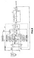
- phase-difference detecting circuit 11 comprises a phase-difference detecting part 12 for detecting a phase difference between a first signal INA with a first frequency and a second signal INB with a second frequency, and a latching part 13 for latching an output of the phase-difference detecting part 12 and outputting it as an output "OUT" of the phase-difference detecting circuit 11.
- the phase-difference detecting part 12 is constituted by a first D flip-flop (DFF1) 14, a second D flip-flop (DFF2) 15, a delay circuit (delay means) 18 comprising inverters 16 and 17, and a 3-input NAND gate (logic means) 19.
- the first D flip-flop (DFF1) 14 has a data terminal D to which the first signal INA different in frequency from the second signal INB is inputted, a clock terminal CK to which the second signal INB is inputted, a reset terminal to which a reset signal RES is inputted, and an output terminal XQ1 connected to an input terminal of the 3-input NAND gate 19.
- the second D flip-flop (DFF2) 15 has a data terminal D to which the first signal INA is inputted, a clock terminal CK to which a third signal INC delayed from the second signal INB by a predetermined time (phase) difference dt by the delay circuit 18 is inputted, a reset terminal to which the reset signal RES is inputted, and an output terminal Q2 connected to an input terminal of the 3-input NAND gate 19.
- the first signal INA with a first frequency is also inputted to the 3-input NAND gate 19.
- the output X of the 3-input NAND gate 19 is outputted to the latching part 13, which is constituted by cross-coupled NAND gates 20, 21 and an inverter 22.
- the NAND gate 20 has an input terminal to which the output X of the 3-input NAND gate 19 is inputted, while the NAND gate 21 has an input terminal to which the reset signal RES is inputted. Accordingly, the same first signal INA is inputted to both the first flip-flop 14 and the second flip-flop 15, and the clock of the second flip-flop 15 is delayed from the clock of the first flip-flop 14 by the time difference dt between the signals INB and INC.
- Fig. 2 schematically illustrates a PLL frequency synthesizer to which the phase-difference detecting circuit 11 is applied.
- the parts substantially identical to corresponding parts of Fig. 10 are designated by the same reference numerals and therefore a detailed description of the identical parts will not be given.
- a PLL integrated circuit (IC) 31 comprises a first AND gate 32 to which a signal OSC IN and a power save control signal PS respectively corresponding to the signals INA and RES of Fig. 1 are inputted, a second AND gate 33 to which the power save control signal PS and a signal f IN (corresponding to the signal INB of Fig.
- phase comparator 3 The output f r of the reference frequency divider 2, the output f v of the comparison frequency divider 4, the power save control signal PS, and the control signal PS1 are inputted to a phase comparator 3.
- the phase comparator 3 is connected to a charge pump 5, which outputs the PLL IC output D o to a low-pass filter 6 connected to the VCO 7.
- the standby control of the phase comparator 3 may be performed by the power save control signal PS instead of the control signal PS1, as shown by the broken line in Fig. 2. In that case, the phase comparator 3 becomes active earlier than the frequency dividers 2 and 4, but there is no problem because the frequency dividers 2 and 4 do not become active until the phases of the signals OSC IN and f IN become small.
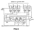
- Fig. 3 schematically illustrates the structure of the divide-by-N frequency divider 4, which is substantially the same as that of the divide-by-R frequency divider 2.
- the Q3 output of the third flip-flop F3 is connected to the LOAD terminals of flip-flops f1 through fn and a NOR gate 34.
- the Q outputs of the flip-flops f1 through fn are connected through inverters to the inputs of a detecting circuit DET for detecting a digital value 4.
- the output of the circuit DET is connected to the D input of the first flip-flop F1.
- the flip-flops f1 through fn is in the dividing-ratio data reading state, and do no go to the counting state even if the clock signal f IN is inputted.
- the flip-flops f1 through fn go to high level, the flip-flops f1 through fn are all reset and the dividing operation will start. Thereafter, the dividing operation is performed according to a predetermined dividing ratio.
- Fig. 4 schematically illustrates the structure of the phase comparator 3 and the charge pump 5.
- the flip-flops Fa and Fb of the phase comparator 3 go to the clear state because the control signal PS1 is low.
- the Q output of the flip-flop Fa goes low, and the XQ output of the flip-flop Fb goes high.
- the P-channel and N-channel MOS transistors of the charge pump 5 are both cut off, and the PLL IC output D o goes to the high impedance state.
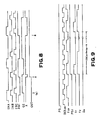
- Figs. 5 and 6 are timing diagrams showing how the phase-difference detecting circuit 11 is operated.
- Fig. 5 shows waveforms when the phase difference t1 between the input signals INA and INB is greater that the phase difference dt between the input signals INB and INC
- Fig. 6 shows waveforms when the phase difference t2 between the input signals INA and INB is less than the phase difference dt between the input signals INB and INC.
- the signals INA and INB are different signals which are not the same in frequency and phase. If, with such a condition, the RES input is not asserted and the two signals INA and INB are inputted, the relationship between the two signals will go to the state shown in Figs. 5 and 6.
- the rising edge of the signal INB leads the rising edge of the signal INA and the phase difference t2 between the two signals INA and INB is within the phase difference dt between the signals INB and INC
- the XQ1 output of the DFF1 will go high because the DFF1 reads the level of the signal INA before the rising edge of the signal INA
- the Q2 output of the DFF2 will go high because the DFF2 reads the level of the signal INA after the rising edge of the signal INA. Since at this time the signal INA is high, the output X of the NAND gate 19 goes low and the output (OUT) of the detecting circuit 11 thus goes low. In this way, the state where the phase difference between the two signals INA and INB is within the phase difference dt between the signals INB and INC is detected.
- the PLL will not be operated because the phase difference is always above a predetermined time difference dt.
- the signals INA and INB are not the same in frequency and phase, and therefore there is a moment that a phase difference t6 becomes less than dt, as shown in Fig. 7(b).
- the charge pump output goes to the high impedance state at the standby time, and the low-pass filter can hold the output voltage when the loop is locked, by the capacity.
- the condition of Fig. 7(a) that the phase difference is always above the predetermined time difference dt cannot occur because the output voltage slightly varies due to the leak current and thus the frequency slightly varies.
- phase difference dt between the signals INB and INC can be easily varied by simply increasing and decreasing the number of the inverters 16 and 17 of the delay circuit 18.
- the phase difference dt between the signals INB and INC is set so that the two low-to-high transitions or high-to-low transitions can quickly match depending on the frequencies of the two signals. For example, when the low-to-high transition of the signal INA does not match with the low-to-high transition of the signal INB, a larger phase difference dt is set.
- the phase-difference detecting circuit 11 the low-to-high transitions of the signals INA and INB are detected at the same time.
- the reset signal RES is therefore inputted to the DFF1, DFF2 and the latching part 13, as shown in Fig. 1.
- the signal INA is inputted to the 3-input NAND gate 19.
- the reasons are as follows. That is, if the signal INA is left unconnected and only the XQ1 and Q2 outputs are connected, the output X of the circuit 11 will go low regardless of the phase difference between the signals INA and INB, as shown in the point A of Fig. 8. Consequently, the output (OUT) of the circuit 11 that is to change at the point B of Fig. 8 will change.
- the reason is that, when the Q2 output of the DFF2 goes high at the point (a) of Fig.
- the Q2 output is delayed by the phase difference dt between the signals INB and INC and therefore the output X of the NAND gate 19 goes to a low level.
- the signal INA is inputted to the NAND gate 19 to eliminate this incorrect operation, and the above described problem is thus overcome.
- Fig. 9 shows a timing diagram when the phase-difference detecting circuit 11 is applied to the PLL IC 31.
- each input gate is then opened, the oscillating output of the external OSC is inputted by the OSC IN signal and enters the phase-difference detecting circuit 11.
- the VCO oscillating output is also inputted by the f IN signal and enters the phase-difference detecting circuit 11. If the rising edges of the two signals become the relationship of Fig. 6, then the control signal PS1 is outputted from the circuit 11 to the frequency dividers 2 and 4. If the frequency dividers 2 and 4 are operated at the same time as the input of the control signal PS1 to the frequency dividers 2 and 4 to output the signals f r and f v to the phase comparator 3, an error signal will become very small and thus the lock-up time can be greatly quickened.
- the transition state where two different frequency signals go high or low at the same time with a predetermined range is detected, and at the same time the counters of the reference frequency divider 2 and comparator frequency divider 4 are operated. Therefore, if the phase-difference detecting circuit 11 according to the present invention is used, for example, in an intermittently operated PLL IC, the reference signal f r and the comparison signal f v which are the same in phase can be produced for a very short time. Consequently, the error signal can be made very small and the lock-up time is thus greatly shortened, so that the performance of the PLL synthesizer is greatly enhanced.
Abstract
Description
- The present invention relates in general to a phase-difference detecting circuit, and in particular to such a circuit that is used in a frequency synthesizer using a PLL (phase-locked loop).
- The phase-locked loop or PLL is a circuit which generates a signal corresponding in phase and frequency to an input signal, and widely used in the control of the number of revolutions of a motor (for example, audio player) and in a frequency synthesizer. When it is desired to make a frequency of oscillation stable and make a frequency variable, an oscillator of the PLL synthesizer type is eminently suited and also used in a FM transmitter.
- With recent extensions in the application of PLLs, improvements in various characteristics for PLLs have been required. For example, improvements in the shortening of a lock-up time and the stability of PLLs have been required. Among frequency synthesizers using a PLL, in order to minimize power consumption of the entire circuit, there is known a frequency synthesizer which intermittently operates the PLL with two modes, which comprise a standby mode that the circuit stops and is thus in the low power consumption state, and an operating mode that the circuit is in the operating state.
- In the intermittent-operation type PLL frequency synthesizer, there are basically two methods of operation stop. One is a method in which a power supply for circuits other than a voltage-controlled oscillator (VCO) in the PLL is turned off, the VCO input voltage is held with the time constant of a low-pass filter, and the VCO output frequency is held at a frequency nearly equal to the frequency of the lock time of the PLL. Another is a method in which a power supply for the entire PLL circuit including a VCO is turned off. In either method, it is necessary that the VCO output oscillating frequency do not largely fluctuate, when the operation of the PLL is started again by turning on the power supply.
- A conventional PLL frequency synthesizer of the above type is shown, for example, in Fig. 10. In the figure, a
reference oscillator 1 comprises a stable crystal oscillator and generates an original signal Xin. Areference divider 2 is programmed to divide the frequency of the original signal Xin from thereference oscillator 1 by the number R, and produces a reference signal fr whose frequency is equal to the frequency of the original signal Xin divided by R.A comparison divider 4 is programmed to divide the frequency of an output signal fin from aVCO 7 by the number N, and produces a variation signal fv whose frequency is equal to the frequency of the VCO output signal fin divided by N.A phase comparator 3 is a phase detecting circuit by logic, and compares the frequency and phase of the reference signal fr with the frequency and phase of the variation signal fv. Thephase comparator 3 outputs comparison outputs EU and ED proportional to the difference in frequency and phase between the two signals fr and fv. If the reference signal fr leads the variation signal fv in phase or fr is higher in frequency than fv (fr > fv), the comparison output EU will go low for a time proportional the difference in phase between the two signals, but the comparison output ED remains high. If, on the other hand, the variation signal fv leads the reference signal fr in phase or fv is higher in frequency than fr (fv > fr), the comparison output ED will go low for a time proportional to the difference in phase between the two signals, but the comparison output EU remains high. If the phases of the reference signal fr and the variation signal fv are the same, the comparison outputs EU and ED will both go high. Acharge pump 5 comprises, for example, P-channel and N-channel MOS (metal-oxide semiconductor) transistors and an inverter. Based on the comparison outputs EU and ED, thecharge pump 5 outputs a signal that will go to the high impedance state when the comparison outputs EU and ED are both high, and outputs a signal that will go high or low when EU is low and ED is high or when EU is high and ED is low. That is, the comparison output EU or ED is low for a time proportional to the difference in phase between the two signals fr and fv, so that the MOS transistors of thecharge pump 5 are turned on to charge or discharge the output lines. By such a function, an error voltage resulting from the phase difference between the two signals fr and fv is produced on the output of a LPF (low-pass filter) 6 connected to thecharge pump 5. TheVCO 7 is an oscillator whose output frequence can be easily varied by changing an externally applied voltage. If the phase of signal fv leads the phase of signal fr, then the VCO oscillating frequency will be decreased until the two signals fr and fv becomes the same in phase. If the phase of signal fr leads the phase of signal fv, then the VCO oscillating frequency will be increased until the two signals fr and fv becomes the same in phase. - In the PLL constructed as described above, on the output terminal of the
VCO 7 is produced a signal which is in phase with the reference signal fr and has a frequency fvco (= N·fr). Therefore, if thecomparison divider 4 comprises a programmable counter and the number N applied to the divider is changed to an arbitrary number by an external control signal, then a signal with a desired frequency can be produced on the VCO output terminal. - However, in the conventional phase-difference detecting circuit having a function of intermittent operation by two modes of a standby mode and an operating mode, when the circuit is alternately operated and stopped at intervals of a predetermined time, the relative phase relationship between the reference signal fr and the comparison signal fv was instable, even if the frequencies of the two signals were made the same by some method at the time the standby mode has been switched to the operating mode. That is, since changing the mode cannot make stable the levels of the flip-flops of the
reference divider 2 andcomparison divider 4, it cannot be predicted which time the signals fr and fv are outputted at. For this reason, if the circuit is operated again in a condition where the phase difference between the signals fr and fv to be supplied to thephase comparator 3 has been large, thephase comparator 3 will tend to output a very large error signal. Since in that case the PLL is operated to reduce the phase difference between the signals fr and fv, the VCO output oscillating frequency fvco largely changes immediately after the operation of the PLL. Consequently, there is the problem that the loop takes a long time to acquire lock. - It is therefore an object of the present invention to provide an improved phase-difference detecting circuit which is used in a PLL frequency synthesizer and the like and which is capable of minimizing the change in the VCO output frequency at the start time of the PLL operation and considerably shortening the time needed to lock the loop in phase and frequency.
- In accordance with one important aspect of the present invention, there is provided a phase comparison circuit comprising phase comparison means for generating an output signal corresponding to the difference in phase between a first input signal and a second input signal, the phase comparison means having an active mode, and a standby mode in which power consumption is reduced; and phase-difference detecting means connected to the phase comparison means for outputting a control signal when the phase difference between the first and second input signals is smaller than a predetermined value. The phase comparison means is switched from the standby mode to the active mode in response to the control signal.
- In accordance with another important aspect of the present invention, there is provided a semiconductor integrated circuit device comprising phase comparison means for generating an output signal corresponding to the difference in phase between a first external input signal and a second external input signal, the phase comparison means having an active mode, and a standby mode in which power consumption is reduced; and phase-difference detecting means connected to the phase comparison means for outputting a control signal when an external power save control signal indicates the switching from the standby mode to the active mode and when the phase difference between the external first and second input signals is smaller than a predetermined value. The phase comparison means is switched from the standby mode to the active mode in response to the control signal.
- In accordance with another important aspect of the present invention, there is provided an intermittent-operation type phase-locked loop system comprising a phase-locked loop circuit for generating an output signal synchronizing in phase with a reference signal, the phase-locked loop circuit having an active mode and a standby mode in which power consumption is reduced, and the phase-locked loop circuit being switched from the active mode to the standby mode in response to a power save control signal; and phase-difference detecting circuit connected to the phase-locked loop circuit for outputting a control signal when the power save control signal is released and when a phase difference between the reference signal and the output signal is smaller than a predetermined value. The phase-locked loop circuit is switched from the standby mode to the active mode in response to the control signal.
- In accordance with another important aspect of the present invention, there is provided a method of reducing the power consumption of a phase-locked loop system, comprising the steps of comparing the phase of a first signal with the phase of a second signal; reducing the power consumption by forcing a part of the phase-locked loop system to a standby state; detecting the difference in phase between the first and second signals; and switching the power reducing step to the phase comparing step when the phase difference is smaller than a predetermined value.
- In accordance with another important aspect of the present invention, there is provided a phase comparison circuit comprising hold means for holding logic levels of two different frequency input signals; and signal output means for outputting a signal informing that there is substantially no phase difference between the two signals, when the two signals held by the hold means rise or fall within a predetermined range.
- In accordance with another important aspect of the present invention, there is provided a phase comparison circuit comprising a first flip-flop having a data input terminal to which a first signal with a first frequency is inputted and a clock input terminal to which a second signal with a second frequency is inputted; delay means for delaying the second signal by a predetermined delay; a second flip-flop having a data input terminal to which the first signal is inputted and a clock input terminal to which an output of the delay means is inputted; logic means to which the first signal, an output of the first flip-flop, and an output of the second flip-flop are inputted; and when the first flip-flop output and the second flip-flop output rise or fall within a predetermined range, a signal for informing that there is substantially no phase difference between the two outputs being outputted by the logic means.
- The above and other objects and advantages will become apparent from the following detailed description when read in conjunction with the accompanying drawings wherein:
- FIG. 1 is a block diagram showing the structure of a phase-difference detecting circuit in accordance with the present invention;
- FIG. 2 is a block diagram showing a PLL frequency synthesizer to which the phase-difference detecting circuit is applied;
- FIG. 3 schematically illustrates the structure of the divide-by-N counter of FIG. 2;
- FIG. 4 schematically illustrates the structure of the phase comparator and charge pump of FIG. 2;
- FIGS. 5 and 6 are timing diagrams showing how the phase-difference detecting circuit is operated;
- FIG. 7(a) shows a condition where the phase difference between input signals INA and INB is always above a predetermined time difference dt;
- FIG. 7(b) shows a condition where the phase difference is less than the predetermined time difference dt;
- FIG. 8 is a timing diagram used to explain the reason that, besides the XQ1 output of the DFF1 and the Q2 output of the DFF2, the signal INA is inputted to the 3-input NAND gate;
- FIG. 9 is a timing diagram showing how the PLL IC of FIG. 2 is operated; and
- FIG. 10 is a block diagram showing the structure of a conventional PLL frequency synthesizer.
- Referring to Fig. 1, there is shown a preferred embodiment of a phase-
difference detecting circuit 11 in accordance with the present invention. The phase-difference detecting circuit 11 comprises a phase-difference detecting part 12 for detecting a phase difference between a first signal INA with a first frequency and a second signal INB with a second frequency, and alatching part 13 for latching an output of the phase-difference detecting part 12 and outputting it as an output "OUT" of the phase-difference detecting circuit 11. The phase-difference detecting part 12 is constituted by a first D flip-flop (DFF1) 14, a second D flip-flop (DFF2) 15, a delay circuit (delay means) 18 comprisinginverters - The first D flip-flop (DFF1) 14 has a data terminal D to which the first signal INA different in frequency from the second signal INB is inputted, a clock terminal CK to which the second signal INB is inputted, a reset terminal to which a reset signal RES is inputted, and an output terminal XQ1 connected to an input terminal of the 3-
input NAND gate 19. Likewise, the second D flip-flop (DFF2) 15 has a data terminal D to which the first signal INA is inputted, a clock terminal CK to which a third signal INC delayed from the second signal INB by a predetermined time (phase) difference dt by thedelay circuit 18 is inputted, a reset terminal to which the reset signal RES is inputted, and an output terminal Q2 connected to an input terminal of the 3-input NAND gate 19. The first signal INA with a first frequency is also inputted to the 3-input NAND gate 19. The output X of the 3-input NAND gate 19 is outputted to thelatching part 13, which is constituted bycross-coupled NAND gates inverter 22. TheNAND gate 20 has an input terminal to which the output X of the 3-input NAND gate 19 is inputted, while theNAND gate 21 has an input terminal to which the reset signal RES is inputted. Accordingly, the same first signal INA is inputted to both the first flip-flop 14 and the second flip-flop 15, and the clock of the second flip-flop 15 is delayed from the clock of the first flip-flop 14 by the time difference dt between the signals INB and INC. - Fig. 2 schematically illustrates a PLL frequency synthesizer to which the phase-
difference detecting circuit 11 is applied. The parts substantially identical to corresponding parts of Fig. 10 are designated by the same reference numerals and therefore a detailed description of the identical parts will not be given. In Fig. 2, a PLL integrated circuit (IC) 31 comprises a first ANDgate 32 to which a signal OSCIN and a power save control signal PS respectively corresponding to the signals INA and RES of Fig. 1 are inputted, a second ANDgate 33 to which the power save control signal PS and a signal fIN (corresponding to the signal INB of Fig. 1) outputted from a VCO are inputted, a programmablereference frequency divider 2 to which the output of the first ANDgate 32 is inputted, and a programmablecomparison frequency divider 4 to which the output of the second ANDgate 33 is inputted. The outputs of the ANDgates difference detecting circuit 11, which detects the phase difference between the two signals OSCIN and fIN and outputs a control signal PS1 corresponding to the output (OUT) of the phase-difference detecting circuit 11 of Fig. 1 to thereference frequency divider 2 and thecomparison frequency divider 4. The output fr of thereference frequency divider 2, the output fv of thecomparison frequency divider 4, the power save control signal PS, and the control signal PS1 are inputted to aphase comparator 3. Thephase comparator 3 is connected to acharge pump 5, which outputs the PLL IC output Do to a low-pass filter 6 connected to theVCO 7. Note that the standby control of thephase comparator 3 may be performed by the power save control signal PS instead of the control signal PS1, as shown by the broken line in Fig. 2. In that case, thephase comparator 3 becomes active earlier than thefrequency dividers frequency dividers - Fig. 3 schematically illustrates the structure of the divide-by-
N frequency divider 4, which is substantially the same as that of the divide-by-R frequency divider 2. The output control signal PS1 from the phase-difference detecting circuit 11 goes low in the standby mode (when PS = 0). If the SET terminals of a first flip-flop F1 and a second flip-flop F2 are low and the CLEAR terminal of a third flip-flop is low, then the Q1 output of the first flip-flop F1 and the Q2 output of the second flip-flop F2 go high, and the Q3 output of the third flip-flop F3 goes low. The Q3 output of the third flip-flop F3 is connected to the LOAD terminals of flip-flops f1 through fn and a NORgate 34. The Q outputs of the flip-flops f1 through fn are connected through inverters to the inputs of a detecting circuit DET for detecting adigital value 4. The output of the circuit DET is connected to the D input of the first flip-flop F1. At the time of the load state (LOAD = low), the flip-flops f1 through fn is in the dividing-ratio data reading state, and do no go to the counting state even if the clock signal fIN is inputted. Since the two inputs of the NORgate 34 are low and high at that time, the output fv of thefrequency divider 4 goes to low. If in the active mode (when PS = 1) the input signals to thefrequency dividers gate 34 are both low at the time the control signal PS1 goes high, and therefore the output fv is outputted. If the control signal PS1 is high, the flip-flops F1, F2 and F3 are all reset, and the count will start when the clock signal fIN makes a low-to-high transition. If the LOAD terminals of the flip-flops f1 through fn go to high level, the flip-flops f1 through fn are all reset and the dividing operation will start. Thereafter, the dividing operation is performed according to a predetermined dividing ratio. - Fig. 4 schematically illustrates the structure of the
phase comparator 3 and thecharge pump 5. In the standby mode (when PS = 0), the flip-flops Fa and Fb of thephase comparator 3 go to the clear state because the control signal PS1 is low. The Q output of the flip-flop Fa goes low, and the XQ output of the flip-flop Fb goes high. At this time, the P-channel and N-channel MOS transistors of thecharge pump 5 are both cut off, and the PLL IC output Do goes to the high impedance state. If the control signal PS1 goes high, then flip-flops Fa and Fb are reset (because one of the two inputs of aNAND gate 35 goes high), and the normal phase comparison operation for detecting the phase difference between the reference signal fr and the variation signal fv is performed. Note that the PLL IC output Do is held to the high impedance state until the phase comparison operation starts. - The operation will hereinafter be described.
- Figs. 5 and 6 are timing diagrams showing how the phase-
difference detecting circuit 11 is operated. Fig. 5 shows waveforms when the phase difference t1 between the input signals INA and INB is greater that the phase difference dt between the input signals INB and INC, while Fig. 6 shows waveforms when the phase difference t2 between the input signals INA and INB is less than the phase difference dt between the input signals INB and INC. Suppose that the signals INA and INB are different signals which are not the same in frequency and phase. If, with such a condition, the RES input is not asserted and the two signals INA and INB are inputted, the relationship between the two signals will go to the state shown in Figs. 5 and 6. - Since in Fig. 5 the phase difference t1 between the two signals INA and INB is above the phase difference dt between the signals INB and INC, the XQ1 output of the D flip-
flop 14 or DFF1 is low and the Q output of the D flip-flop 15 or DFF2 is high, so that the output (OUT) of the phase-difference detecting circuit 11 remains low. - If, as shown in Fig. 6, the rising edge of the signal INB leads the rising edge of the signal INA and the phase difference t2 between the two signals INA and INB is within the phase difference dt between the signals INB and INC, the XQ1 output of the DFF1 will go high because the DFF1 reads the level of the signal INA before the rising edge of the signal INA, and the Q2 output of the DFF2 will go high because the DFF2 reads the level of the signal INA after the rising edge of the signal INA. Since at this time the signal INA is high, the output X of the
NAND gate 19 goes low and the output (OUT) of the detectingcircuit 11 thus goes low. In this way, the state where the phase difference between the two signals INA and INB is within the phase difference dt between the signals INB and INC is detected. - If, as shown in Fig. 7(a), the frequencies of the input signals INA and INB both do not vary and the phase difference t1 is greater than dt, the PLL will not be operated because the phase difference is always above a predetermined time difference dt. In order to avoid this condition, the signals INA and INB are not the same in frequency and phase, and therefore there is a moment that a phase difference t6 becomes less than dt, as shown in Fig. 7(b). In fact, in the intermittent operation of a PLL, the charge pump output goes to the high impedance state at the standby time, and the low-pass filter can hold the output voltage when the loop is locked, by the capacity. However, the condition of Fig. 7(a) that the phase difference is always above the predetermined time difference dt cannot occur because the output voltage slightly varies due to the leak current and thus the frequency slightly varies.
- Note that the phase difference dt between the signals INB and INC can be easily varied by simply increasing and decreasing the number of the
inverters delay circuit 18. The phase difference dt between the signals INB and INC is set so that the two low-to-high transitions or high-to-low transitions can quickly match depending on the frequencies of the two signals. For example, when the low-to-high transition of the signal INA does not match with the low-to-high transition of the signal INB, a larger phase difference dt is set. In the phase-difference detecting circuit 11, the low-to-high transitions of the signals INA and INB are detected at the same time. If the output (OUT) of the phase-difference detecting circuit 11 changes, it will be necessary to reset the circuit to detect the low-to-high transition after that time. The reset signal RES is therefore inputted to the DFF1, DFF2 and the latchingpart 13, as shown in Fig. 1. - In the embodiment of Fig. 1, in addition to the XQ1 output of the DFF1 and the Q2 output of the DFF2, the signal INA is inputted to the 3-
input NAND gate 19. The reasons are as follows. That is, if the signal INA is left unconnected and only the XQ1 and Q2 outputs are connected, the output X of thecircuit 11 will go low regardless of the phase difference between the signals INA and INB, as shown in the point A of Fig. 8. Consequently, the output (OUT) of thecircuit 11 that is to change at the point B of Fig. 8 will change. The reason is that, when the Q2 output of the DFF2 goes high at the point (a) of Fig. 8 and at the point A the XQ1 output of the DFF1 goes high and the Q2 output goes low, the Q2 output is delayed by the phase difference dt between the signals INB and INC and therefore the output X of theNAND gate 19 goes to a low level. In the embodiment of Fig. 1, the signal INA is inputted to theNAND gate 19 to eliminate this incorrect operation, and the above described problem is thus overcome. - Fig. 9 shows a timing diagram when the phase-
difference detecting circuit 11 is applied to thePLL IC 31. In the figure, suppose now that thePLL IC 31 is in the standby mode (PS = low). With this state, each counter goes to the reset state, the charge pump output goes to the high impedance state. Therefore, since the voltage at the time of lock is held by the CR time constant of the low-pass filter 6, theexternal VCO 7 ideally oscillates at a frequency fIN of the lock time, but in fact the VCO oscillating frequency slightly changes due to leak. - If the standby mode is switched to the operating mode, each input gate is then opened, the oscillating output of the external OSC is inputted by the OSCIN signal and enters the phase-
difference detecting circuit 11. The VCO oscillating output is also inputted by the fIN signal and enters the phase-difference detecting circuit 11. If the rising edges of the two signals become the relationship of Fig. 6, then the control signal PS1 is outputted from thecircuit 11 to thefrequency dividers frequency dividers frequency dividers phase comparator 3, an error signal will become very small and thus the lock-up time can be greatly quickened. - Thus, in the present invention, the transition state where two different frequency signals go high or low at the same time with a predetermined range is detected, and at the same time the counters of the
reference frequency divider 2 andcomparator frequency divider 4 are operated. Therefore, if the phase-difference detecting circuit 11 according to the present invention is used, for example, in an intermittently operated PLL IC, the reference signal fr and the comparison signal fv which are the same in phase can be produced for a very short time. Consequently, the error signal can be made very small and the lock-up time is thus greatly shortened, so that the performance of the PLL synthesizer is greatly enhanced. - The invention has been described with reference to the preferred embodiment. Obviously modifications and alternations will occur to others upon a reading and understanding of this application. It is intended to include all such modifications and alternations insofar as they come within the scope of the appended claims or the equivalents thereof.
Claims (13)
phase comparison means for generating an output signal corresponding to the difference in phase between a first input signal and a second input signal, the phase comparison means having an active mode, and a standby mode in which power consumption is reduced; and
phase-difference detecting means connected to said phase comparison means for outputting a control signal when the phase difference between said first and second input signals is smaller than a predetermined value;
said phase comparison means being switched from said standby mode to said active mode in response to said control signal.
a first flip-flop having a data input terminal to which said first input signal is inputted and a clock input terminal to which said second input signal is inputted;
delay means for delaying said second input signal by a predetermined delay;
a second flip-flop having a data input terminal to which said first input signal is inputted and a clock input terminal to which an output of said delay means is inputted;
logic means to which said first input signal, an output of said first flip-flop, and an output of said second flip-flop are inputted; and
when said first flip-flop output and said second flip-flop output rise or fall within a predetermined range, a signal for informing that there is substantially no phase difference between said two outputs being outputted by said logic means.
phase comparison means for generating an output signal corresponding to the difference in phase between a first external input signal and a second external input signal, the phase comparison means having an active mode, and a standby mode in which power consumption is reduced; and
phase-difference detecting means connected to said phase comparison means for outputting a control signal when an external power save control signal indicates the switching from said standby mode to said active mode and when said phase difference between said external first and second input signals is smaller than a predetermined value;
said phase comparison means being switched from said standby mode to said active mode in response to said control signal.
a first gate circuit having input terminals to which said first external input signal and said external power save control signal are inputted, and an output terminal connected to said first frequency divider; and
a second gate circuit having input terminals to which said second external input signal and said external power save control signal are inputted, and an output terminal connected to said first frequency divider;
said first and second gate circuits allowing said first and second external input signals to pass therethrough when said external power save control signal is active, and preventing said first and second external input signals from passing therethrough when said external power save control signal is inactive.
a phase-locked loop circuit for generating an output signal synchronizing in phase with a reference signal, the phase-locked loop circuit having an active mode and a standby mode in which power consumption is reduced, and the phase-locked loop circuit being switched from said active mode to said standby mode in response to a power save control signal; and
phase-difference detecting circuit connected to said phase-locked loop circuit for outputting a control signal when said power save control signal is released and when a phase difference between said reference signal and said output signal is smaller than a predetermined value;
said phase-locked loop circuit being switched from said standby mode to said active mode in response to said control signal.
comparing the phase of a first signal with the phase of a second signal;
reducing said power consumption by forcing a part of said phase-locked loop system to a standby state;
detecting the difference in phase between said first and second signals; and
switching the power reducing step to the phase comparing step when said phase difference is smaller than a predetermined value.
hold means for holding logic levels of two different frequency input signals; and
signal output means for outputting a signal informing that there is substantially no phase difference between said two signals, when said two signals held by said hold means rise or fall within a predetermined range.
a first flip-flop having a data input terminal to which a first signal with a first frequency is inputted and a clock input terminal to which a second signal with a second frequency is inputted;
delay means for delaying said second signal by a predetermined delay;
a second flip-flop having a data input terminal to which said first signal is inputted and a clock input terminal to which an output of said delay means is inputted;
logic means to which said first signal, an output of said first flip-flop, and an output of said second flip-flop are inputted; and
when said first flip-flop output and said second flip-flop output rise or fall within a predetermined range, a signal for informing that there is substantially no phase difference between said two outputs being outputted by said logic means.
Applications Claiming Priority (2)
| Application Number | Priority Date | Filing Date | Title |
|---|---|---|---|
| JP152901/89 | 1989-06-14 | ||
| JP1152901A JP2795323B2 (en) | 1989-06-14 | 1989-06-14 | Phase difference detection circuit |
Publications (3)
| Publication Number | Publication Date |
|---|---|
| EP0402736A2 true EP0402736A2 (en) | 1990-12-19 |
| EP0402736A3 EP0402736A3 (en) | 1991-05-08 |
| EP0402736B1 EP0402736B1 (en) | 1996-04-24 |
Family
ID=15550613
Family Applications (1)
| Application Number | Title | Priority Date | Filing Date |
|---|---|---|---|
| EP90110584A Expired - Lifetime EP0402736B1 (en) | 1989-06-14 | 1990-06-05 | Phase-difference detecting circuit |
Country Status (5)
| Country | Link |
|---|---|
| US (1) | US5103192A (en) |
| EP (1) | EP0402736B1 (en) |
| JP (1) | JP2795323B2 (en) |
| KR (1) | KR940005934B1 (en) |
| DE (1) | DE69026646T2 (en) |
Cited By (12)
| Publication number | Priority date | Publication date | Assignee | Title |
|---|---|---|---|---|
| EP0492433A2 (en) * | 1990-12-26 | 1992-07-01 | Motorola, Inc. | Method for placing a frequency synthesizer into standby mode and apparatus therefor |
| US5493242A (en) * | 1993-06-30 | 1996-02-20 | Vlsi Technology, Inc. | Status register with asynchronous read and reset and method for providing same |
| WO1998016005A1 (en) * | 1996-10-07 | 1998-04-16 | Peregrine Semiconductor Corporation | Phase detector with explicit asynchronous reset |
| EP0942553A2 (en) * | 1998-03-12 | 1999-09-15 | Nec Corporation | Oversampling type clock recovery circuit with power consumption reduced |
| EP0942552A2 (en) * | 1998-03-12 | 1999-09-15 | Nec Corporation | Over-sampling type clock recovery circuit with power consumption reduced |
| US7064617B2 (en) | 2003-05-02 | 2006-06-20 | Silicon Laboratories Inc. | Method and apparatus for temperature compensation |
| US7187241B2 (en) | 2003-05-02 | 2007-03-06 | Silicon Laboratories Inc. | Calibration of oscillator devices |
| US7288998B2 (en) | 2003-05-02 | 2007-10-30 | Silicon Laboratories Inc. | Voltage controlled clock synthesizer |
| US7295077B2 (en) | 2003-05-02 | 2007-11-13 | Silicon Laboratories Inc. | Multi-frequency clock synthesizer |
| WO2008006818A3 (en) * | 2006-07-13 | 2008-06-12 | Siemens Ag | Radar system |
| US7436227B2 (en) | 2003-05-02 | 2008-10-14 | Silicon Laboratories Inc. | Dual loop architecture useful for a programmable clock source and clock multiplier applications |
| CN110476349A (en) * | 2017-03-24 | 2019-11-19 | 罗姆股份有限公司 | The driving circuit of load, the system using the driving circuit, the control method of driving circuit |
Families Citing this family (31)
| Publication number | Priority date | Publication date | Assignee | Title |
|---|---|---|---|---|
| US5335365A (en) * | 1991-07-08 | 1994-08-02 | Motorola, Inc. | Frequency synthesizer with VCO output control |
| US5298866A (en) * | 1992-06-04 | 1994-03-29 | Kaplinsky Cecil H | Clock distribution circuit with active de-skewing |
| US5568513A (en) * | 1993-05-11 | 1996-10-22 | Ericsson Inc. | Standby power savings with cumulative parity check in mobile phones |
| JP3643385B2 (en) * | 1993-05-19 | 2005-04-27 | 株式会社東芝 | Semiconductor circuit device |
| JP2636677B2 (en) * | 1993-06-02 | 1997-07-30 | 日本電気株式会社 | Semiconductor integrated circuit |
| US5406613A (en) * | 1993-06-29 | 1995-04-11 | Pacific Communication Sciences, Inc. | Method and apparatus for reducing power consumption in cellular telephone by adaptively determining the reliability of the reception of a received message block |
| US5493700A (en) * | 1993-10-29 | 1996-02-20 | Motorola | Automatic frequency control apparatus |
| KR100190149B1 (en) * | 1993-11-09 | 1999-06-01 | 조나단 피. 메이어 | Error suppressing circuit and method therefor for a phase locked loop |
| US5742650A (en) * | 1994-02-04 | 1998-04-21 | Motorola, Inc. | Power reduction method and apparatus for phase-locked loop based clocks in a data processing system |
| US5794130A (en) * | 1994-04-26 | 1998-08-11 | Funai Electric Engineering Company Limited | Wireless communication system having improved PLL circuits |
| US6804726B1 (en) * | 1996-05-22 | 2004-10-12 | Geovector Corporation | Method and apparatus for controlling electrical devices in response to sensed conditions |
| JPH10308667A (en) | 1997-05-02 | 1998-11-17 | Nec Corp | Pll frequency synthesizer |
| CN1115779C (en) * | 1997-05-21 | 2003-07-23 | 三星电子株式会社 | Digital phase locked loop circuit and method therefor |
| DE19736464A1 (en) * | 1997-08-21 | 1999-03-04 | Siemens Ag | Method and device for setting the oscillation frequency of an oscillator |
| US6069506A (en) * | 1998-05-20 | 2000-05-30 | Micron Technology, Inc. | Method and apparatus for improving the performance of digital delay locked loop circuits |
| DE19837204B4 (en) | 1998-08-17 | 2006-06-08 | Telefonaktiebolaget Lm Ericsson (Publ) | Dead-time reduction in frequency jumps in multiband synthesis units |
| US6223047B1 (en) | 1998-08-26 | 2001-04-24 | Telefonaktiebolaget Lm Ericsson (Publ) | Extended sleep mode method and apparatus |
| FR2790887B1 (en) * | 1999-03-09 | 2003-01-03 | Univ Joseph Fourier | LOGIC CIRCUIT PROTECTED AGAINST TRANSIENT INTERFERENCE |
| US8230279B2 (en) * | 1999-03-09 | 2012-07-24 | iRoctechnologies | Logic circuit protected against transient disturbances |
| DE19929178C2 (en) * | 1999-06-25 | 2002-10-24 | Infineon Technologies Ag | Phase locked loop system |
| EP1123580B1 (en) * | 1999-08-24 | 2005-11-09 | Koninklijke Philips Electronics N.V. | Charge pump phase locked loop circuit |
| US6459309B2 (en) * | 2000-03-10 | 2002-10-01 | Koninklijke Philips Electronics N.V. | Frequency converter enabling a non-integer division ratio to be programmed by means of a unique control word |
| US6278304B1 (en) | 2000-03-23 | 2001-08-21 | International Business Machines Corporation | Look-ahead enabling charge pump in phase-locked loop circuits |
| US7027796B1 (en) * | 2001-06-22 | 2006-04-11 | Rfmd Wpan, Inc. | Method and apparatus for automatic fast locking power conserving synthesizer |
| US7184798B1 (en) * | 2002-10-03 | 2007-02-27 | National Semiconductor Corporation | Power conservation system and method |
| KR100526349B1 (en) * | 2002-11-14 | 2005-11-08 | 엘지전자 주식회사 | Circuit for detecting phase |
| ATE331341T1 (en) * | 2002-12-13 | 2006-07-15 | Koninkl Philips Electronics Nv | LOW LOCKING TIME DELAY LOCKED CONTROL LOOP WITH THE USE OF A TIME CYCLE SUPPRESSION DEVICE |
| US7855584B2 (en) * | 2003-12-09 | 2010-12-21 | St-Ericsson Sa | Low lock time delay locked loops using time cycle suppressor |
| KR100711103B1 (en) * | 2004-12-22 | 2007-04-24 | 삼성전자주식회사 | Adoptive Tri-State Phase Frequency Detector and Method thereof, and Phase Lock Loop |
| FR2954551B1 (en) * | 2009-12-21 | 2012-08-17 | Commissariat Energie Atomique | SECURE NON-CONTACT DATA EXCHANGE DEVICE BETWEEN A READER AND A CARD |
| US20130154594A1 (en) * | 2011-12-16 | 2013-06-20 | Texas Instruments Incorporated | Electronic device and method for power measurement |
Citations (2)
| Publication number | Priority date | Publication date | Assignee | Title |
|---|---|---|---|---|
| EP0132196A1 (en) * | 1983-07-19 | 1985-01-23 | Thomson-Csf | Frequency synthesizer for a television receiver |
| EP0272938A2 (en) * | 1986-12-23 | 1988-06-29 | Nippon Telegraph And Telephone Corporation | Frequency synthesizer |
Family Cites Families (3)
| Publication number | Priority date | Publication date | Assignee | Title |
|---|---|---|---|---|
| US4631496A (en) * | 1981-04-06 | 1986-12-23 | Motorola, Inc. | Battery saving system for a frequency synthesizer |
| JPH0693629B2 (en) * | 1987-07-08 | 1994-11-16 | 株式会社日立製作所 | Phase locked loop circuit with drift detection function |
| US4893094A (en) * | 1989-03-13 | 1990-01-09 | Motorola, Inc. | Frequency synthesizer with control of start-up battery saving operations |
-
1989
- 1989-06-14 JP JP1152901A patent/JP2795323B2/en not_active Expired - Fee Related
-
1990
- 1990-06-05 EP EP90110584A patent/EP0402736B1/en not_active Expired - Lifetime
- 1990-06-05 DE DE69026646T patent/DE69026646T2/en not_active Expired - Fee Related
- 1990-06-06 US US07/534,618 patent/US5103192A/en not_active Expired - Lifetime
- 1990-06-13 KR KR1019900008663A patent/KR940005934B1/en not_active IP Right Cessation
Patent Citations (2)
| Publication number | Priority date | Publication date | Assignee | Title |
|---|---|---|---|---|
| EP0132196A1 (en) * | 1983-07-19 | 1985-01-23 | Thomson-Csf | Frequency synthesizer for a television receiver |
| EP0272938A2 (en) * | 1986-12-23 | 1988-06-29 | Nippon Telegraph And Telephone Corporation | Frequency synthesizer |
Non-Patent Citations (1)
| Title |
|---|
| 37TH IEEE VEHICULAR TECHNOLOGY CONFERENCE, Tampa, Florida, 1st - 3rd June 1987, pages 435-440, IEEE, New York, US; J. NAKAGAWA et al.: "Handheld telephone for 800MHz-band cellular radio systems" * |
Cited By (19)
| Publication number | Priority date | Publication date | Assignee | Title |
|---|---|---|---|---|
| EP0492433A2 (en) * | 1990-12-26 | 1992-07-01 | Motorola, Inc. | Method for placing a frequency synthesizer into standby mode and apparatus therefor |
| EP0492433A3 (en) * | 1990-12-26 | 1993-05-05 | Motorola, Inc. | Method for placing a frequency synthesizer into standby mode and apparatus therefor |
| US5493242A (en) * | 1993-06-30 | 1996-02-20 | Vlsi Technology, Inc. | Status register with asynchronous read and reset and method for providing same |
| US5596288A (en) * | 1993-06-30 | 1997-01-21 | Vlsi Technology, Inc. | Status register with asynchronous read and reset and method for providing same |
| WO1998016005A1 (en) * | 1996-10-07 | 1998-04-16 | Peregrine Semiconductor Corporation | Phase detector with explicit asynchronous reset |
| EP0942553A3 (en) * | 1998-03-12 | 2004-01-02 | NEC Electronics Corporation | Oversampling type clock recovery circuit with power consumption reduced |
| EP0942552A2 (en) * | 1998-03-12 | 1999-09-15 | Nec Corporation | Over-sampling type clock recovery circuit with power consumption reduced |
| EP0942552A3 (en) * | 1998-03-12 | 2003-12-17 | NEC Electronics Corporation | Over-sampling type clock recovery circuit with power consumption reduced |
| EP0942553A2 (en) * | 1998-03-12 | 1999-09-15 | Nec Corporation | Oversampling type clock recovery circuit with power consumption reduced |
| US7295077B2 (en) | 2003-05-02 | 2007-11-13 | Silicon Laboratories Inc. | Multi-frequency clock synthesizer |
| US7187241B2 (en) | 2003-05-02 | 2007-03-06 | Silicon Laboratories Inc. | Calibration of oscillator devices |
| US7288998B2 (en) | 2003-05-02 | 2007-10-30 | Silicon Laboratories Inc. | Voltage controlled clock synthesizer |
| US7064617B2 (en) | 2003-05-02 | 2006-06-20 | Silicon Laboratories Inc. | Method and apparatus for temperature compensation |
| US7436227B2 (en) | 2003-05-02 | 2008-10-14 | Silicon Laboratories Inc. | Dual loop architecture useful for a programmable clock source and clock multiplier applications |
| US7825708B2 (en) | 2003-05-02 | 2010-11-02 | Silicon Laboratories Inc. | Dual loop architecture useful for a programmable clock source and clock multiplier applications |
| WO2008006818A3 (en) * | 2006-07-13 | 2008-06-12 | Siemens Ag | Radar system |
| US7990313B2 (en) | 2006-07-13 | 2011-08-02 | Siemens Aktiengesellschaft | Radar arrangement |
| CN110476349A (en) * | 2017-03-24 | 2019-11-19 | 罗姆股份有限公司 | The driving circuit of load, the system using the driving circuit, the control method of driving circuit |
| CN110476349B (en) * | 2017-03-24 | 2023-03-28 | 罗姆股份有限公司 | Load driving circuit, system using the same, and method for controlling the driving circuit |
Also Published As
| Publication number | Publication date |
|---|---|
| US5103192A (en) | 1992-04-07 |
| KR940005934B1 (en) | 1994-06-24 |
| EP0402736A3 (en) | 1991-05-08 |
| EP0402736B1 (en) | 1996-04-24 |
| JP2795323B2 (en) | 1998-09-10 |
| DE69026646D1 (en) | 1996-05-30 |
| DE69026646T2 (en) | 1996-09-12 |
| KR910002135A (en) | 1991-01-31 |
| JPH0318122A (en) | 1991-01-25 |
Similar Documents
| Publication | Publication Date | Title |
|---|---|---|
| US5103192A (en) | Phase-difference detecting circuit and method of reducing power consumption in a pll system | |
| US7053666B2 (en) | Phase frequency detector | |
| US7176763B2 (en) | Phase-locked loop integrated circuits having fast phase locking characteristics | |
| JP2710214B2 (en) | Phase locked loop circuit | |
| US5870002A (en) | Phase-frequency lock detector | |
| US6150889A (en) | Circuit and method for minimizing recovery time | |
| JP2009065704A (en) | Method for reducing noise in phase-locked loop frequency composition | |
| JPH07202690A (en) | Clock signal generation circuit | |
| US6525612B2 (en) | Mode control of PLL circuit | |
| US7332945B2 (en) | Divider having dual modulus pre-scaler and an associated method | |
| EP2359469B1 (en) | A phase frequency detector | |
| JPH10242856A (en) | Variable speed phase locked loop system and its method | |
| EP1246369B1 (en) | Mode switching method for PLL circuit and mode control circuit for PLL circuit | |
| KR100510523B1 (en) | Phase-frequency detector providing for reflecting clock transitions at an added delay for a zero dead zone in charge pump control and phase/frequency detection method thereof | |
| US20020041214A1 (en) | PLL circuit | |
| KR100299195B1 (en) | Variable frequency divider and pll circuit | |
| US6121845A (en) | Phase-locked loop system and method for modifying an output transition time | |
| US20030214330A1 (en) | Phase-locked loop circuit | |
| US20080111637A1 (en) | Voltage controlled oscillator and pll having the same | |
| KR20080014440A (en) | Circuits and method for locking fast in phase lock frequency synthesizer | |
| JP3079943B2 (en) | PLL circuit | |
| KR100345397B1 (en) | Frequency synthesizer having high speed | |
| JPH11205135A (en) | Phase locked loop circuit | |
| JP2002217725A (en) | Pll frequency synthesizer | |
| JPH06104747A (en) | Phase locked loop circuit |
Legal Events
| Date | Code | Title | Description |
|---|---|---|---|
| PUAI | Public reference made under article 153(3) epc to a published international application that has entered the european phase |
Free format text: ORIGINAL CODE: 0009012 |
|
| AK | Designated contracting states |
Kind code of ref document: A2 Designated state(s): DE FR GB |
|
| PUAL | Search report despatched |
Free format text: ORIGINAL CODE: 0009013 |
|
| AK | Designated contracting states |
Kind code of ref document: A3 Designated state(s): DE FR GB |
|
| 17P | Request for examination filed |
Effective date: 19910606 |
|
| 17Q | First examination report despatched |
Effective date: 19930820 |
|
| GRAH | Despatch of communication of intention to grant a patent |
Free format text: ORIGINAL CODE: EPIDOS IGRA |
|
| GRAA | (expected) grant |
Free format text: ORIGINAL CODE: 0009210 |
|
| AK | Designated contracting states |
Kind code of ref document: B1 Designated state(s): DE FR GB |
|
| REF | Corresponds to: |
Ref document number: 69026646 Country of ref document: DE Date of ref document: 19960530 |
|
| ET | Fr: translation filed | ||
| PLBE | No opposition filed within time limit |
Free format text: ORIGINAL CODE: 0009261 |
|
| STAA | Information on the status of an ep patent application or granted ep patent |
Free format text: STATUS: NO OPPOSITION FILED WITHIN TIME LIMIT |
|
| 26N | No opposition filed | ||
| REG | Reference to a national code |
Ref country code: GB Ref legal event code: IF02 |
|
| PGFP | Annual fee paid to national office [announced via postgrant information from national office to epo] |
Ref country code: GB Payment date: 20050601 Year of fee payment: 16 |
|
| PGFP | Annual fee paid to national office [announced via postgrant information from national office to epo] |
Ref country code: DE Payment date: 20050602 Year of fee payment: 16 |
|
| PGFP | Annual fee paid to national office [announced via postgrant information from national office to epo] |
Ref country code: FR Payment date: 20050608 Year of fee payment: 16 |
|
| PG25 | Lapsed in a contracting state [announced via postgrant information from national office to epo] |
Ref country code: GB Free format text: LAPSE BECAUSE OF NON-PAYMENT OF DUE FEES Effective date: 20060605 |
|
| PG25 | Lapsed in a contracting state [announced via postgrant information from national office to epo] |
Ref country code: DE Free format text: LAPSE BECAUSE OF NON-PAYMENT OF DUE FEES Effective date: 20070103 |
|
| GBPC | Gb: european patent ceased through non-payment of renewal fee |
Effective date: 20060605 |
|
| REG | Reference to a national code |
Ref country code: FR Ref legal event code: ST Effective date: 20070228 |
|
| PG25 | Lapsed in a contracting state [announced via postgrant information from national office to epo] |
Ref country code: FR Free format text: LAPSE BECAUSE OF NON-PAYMENT OF DUE FEES Effective date: 20060630 |