EP0387834A2 - Semiconductor structure for processing and storing of information - Google Patents
Semiconductor structure for processing and storing of information Download PDFInfo
- Publication number
- EP0387834A2 EP0387834A2 EP90104813A EP90104813A EP0387834A2 EP 0387834 A2 EP0387834 A2 EP 0387834A2 EP 90104813 A EP90104813 A EP 90104813A EP 90104813 A EP90104813 A EP 90104813A EP 0387834 A2 EP0387834 A2 EP 0387834A2
- Authority
- EP
- European Patent Office
- Prior art keywords
- functional block
- semiconductor device
- conductive wires
- directions
- memory cell
- Prior art date
- Legal status (The legal status is an assumption and is not a legal conclusion. Google has not performed a legal analysis and makes no representation as to the accuracy of the status listed.)
- Ceased
Links
Images

Classifications
-
- H—ELECTRICITY
- H10—SEMICONDUCTOR DEVICES; ELECTRIC SOLID-STATE DEVICES NOT OTHERWISE PROVIDED FOR
- H10B—ELECTRONIC MEMORY DEVICES
- H10B20/00—Read-only memory [ROM] devices
-
- H—ELECTRICITY
- H10—SEMICONDUCTOR DEVICES; ELECTRIC SOLID-STATE DEVICES NOT OTHERWISE PROVIDED FOR
- H10B—ELECTRONIC MEMORY DEVICES
- H10B53/00—Ferroelectric RAM [FeRAM] devices comprising ferroelectric memory capacitors
- H10B53/30—Ferroelectric RAM [FeRAM] devices comprising ferroelectric memory capacitors characterised by the memory core region
-
- H—ELECTRICITY
- H01—ELECTRIC ELEMENTS
- H01L—SEMICONDUCTOR DEVICES NOT COVERED BY CLASS H10
- H01L27/00—Devices consisting of a plurality of semiconductor or other solid-state components formed in or on a common substrate
- H01L27/02—Devices consisting of a plurality of semiconductor or other solid-state components formed in or on a common substrate including semiconductor components specially adapted for rectifying, oscillating, amplifying or switching and having at least one potential-jump barrier or surface barrier; including integrated passive circuit elements with at least one potential-jump barrier or surface barrier
- H01L27/04—Devices consisting of a plurality of semiconductor or other solid-state components formed in or on a common substrate including semiconductor components specially adapted for rectifying, oscillating, amplifying or switching and having at least one potential-jump barrier or surface barrier; including integrated passive circuit elements with at least one potential-jump barrier or surface barrier the substrate being a semiconductor body
- H01L27/10—Devices consisting of a plurality of semiconductor or other solid-state components formed in or on a common substrate including semiconductor components specially adapted for rectifying, oscillating, amplifying or switching and having at least one potential-jump barrier or surface barrier; including integrated passive circuit elements with at least one potential-jump barrier or surface barrier the substrate being a semiconductor body including a plurality of individual components in a repetitive configuration
-
- H—ELECTRICITY
- H01—ELECTRIC ELEMENTS
- H01L—SEMICONDUCTOR DEVICES NOT COVERED BY CLASS H10
- H01L27/00—Devices consisting of a plurality of semiconductor or other solid-state components formed in or on a common substrate
-
- H—ELECTRICITY
- H10—SEMICONDUCTOR DEVICES; ELECTRIC SOLID-STATE DEVICES NOT OTHERWISE PROVIDED FOR
- H10B—ELECTRONIC MEMORY DEVICES
- H10B20/00—Read-only memory [ROM] devices
- H10B20/60—Peripheral circuit regions
- H10B20/65—Peripheral circuit regions of memory structures of the ROM only type
-
- H—ELECTRICITY
- H10—SEMICONDUCTOR DEVICES; ELECTRIC SOLID-STATE DEVICES NOT OTHERWISE PROVIDED FOR
- H10B—ELECTRONIC MEMORY DEVICES
- H10B53/00—Ferroelectric RAM [FeRAM] devices comprising ferroelectric memory capacitors
Definitions
- the present invention relates to a semiconductor device formed on a semiconductor substrate, and more particularly to a semiconductor device wherein elements for processing information and elements for storing information are formed on a single semiconductor substrate.
- a semiconductor device With recent developments in semiconductor technology, a semiconductor device have been practically realized which has a great number of functional elements formed on a single semiconductor substrate. For example, there has been realized a semiconductor device having within its semiconductor substrate a CPU (Central Processing Unit) for performing logical operations, data control and the like, a ROM (Read Only Memory) for storing fixed data such as operating system (OS) and the like, a RAM (Random Access Memory) for storing temporary data, and other elements.
- a semiconductor device includes almost all functional elements necessary for a computer in one chip. A very compact device with great information processing capability is thus realized and has wide application to such as IC cards.
- Such a semiconductor device has been desired to have a more sophisticated function as its memory capacity increases and its logical circuits become large scaled. The reason for this is that devices which can process more information at higher speeds are becoming necessary. In order to meet such requirements, it is necessary to integrate elements as much as possible on a single semiconductor substrate. It therefore becomes necessary to make each element smaller. If not possible, the chip area will increase to pose a number of problems associated with manufacturing techniques, resulting in a difficulty in mass-producing devices of low cost.
- the present invention has been made in consideration of the above problems. It is an object of the present invention to provide a semiconductor device having both a large memory capacity and a highly sophisticated information processing capability and being formed on a single semiconductor substrate without any increase of the chip area and without the need of severe miniaturization of elements.
- a first functional block for data processing and a memory cell array of a second functional block for storage of various information necessary for the data processing are laminated, as an upper layer and lower layer on a single semiconductor substrate, a first functional block for data processing and a memory cell array of a second functional block for storage of various information necessary for the data processing.
- the overall dimensions of the semiconductor device can be made small when compared with a device which forms both the first and second functional blocks on the same surface.
- the miniaturization of the semiconductor device can be achieved without reducing the size of each of semiconductor elements constituting the first and second functional blocks small. There is no need therefore to miniaturize each semiconductor element, and hence there is no fear of lowering the reliability which might be caused by miniaturization.
- the information necessary for the data processing by the first functional block is previously stored in the memory cell array.
- virtual intersections three-dimensional intersections between conductive wires in the X- and Y-directions are optionally made conductive, or the state of ferroelectric members at virtual intersections is optionally changed. Accordingly, the information necessary for the data processing by the first functional block can be previously stored in the memory cell array of the second functional block. In other words, the information necessary for a particular user of this device can be previously stored in the memory cell array.
- the overall dimensions of a semiconductor device can be made small without reducing the size of each semiconductor element small.
- the difficulty in manufacturing is not increased, thereby not only allowing devices of low cost but also presenting no fear of lowering the reliability which might be caused through miniaturization.
- the memory capacity can be increased and the data processing functions can be highly sophisticated assuming that a device having the same dimensions as a conventional one is used.
- the information necessary for the data processing can be previously stored in the memory cell array.
- a user can optionally store in the memory cell the information necessary for the data processing, and in addition, information once stored can be rewritten.
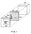
- Fig. 1 is a schematic view illustrating the concept of the present invention.
- the embodiment semiconductor device has a lower layer 200 and an upper layer 300 laminated one upon the other on a semiconductor substrate 100.
- the lower layer 200 includes a first functional block (data processing section) and a part (constructed of transistors) of a second functional block (memory section).
- the upper layer 300 includes the remaining part (not including transistors) of the second functional block.
- the first functional block has a function of performing logical operations, data control and the like, and is shown as a CPU 202 in Fig. 1.
- the second functional block is used for storing information, a part of the first functional block being shown in Fig. 1 as a memory cell array 302 of ROM in the upper layer 300 and a RAM 204 and a peripheral circuit (decoder, control unit, input/output unit and the like) 206 of ROM in the lower layer 200.
- Figs. 2A to 2C are cross sections illustrating the manufacturing processes of a semiconductor device according to the first embodiment which is an example of the device conceptually shown in Fig. 1.
- the first embodiment operates as a mask ROM.
- a semiconductor substrate P-type silicon substrate
- N-channel transistor 101 and P-channel transistor 102 as the data processing section.
- Reference numeral 103 represents an N-type well provided for the P-channel transistor 102.
- N-channel transistor 104 and a P-channel transistor 105 which constitute the peripheral circuit of the memory section, e.g., a decoder, control unit, input/output unit and the like.
- Reference numeral 106 represents an N-type well provided for the P-channel transistor 105.
- Reference numeral 108 represents a passivation film deposited for protecting the elements, the passivation film being made of SiO2 or PSG formed by a CVD method.
- Contact holes 108a, 108a, ... are formed in the passivation film 108 where necessary, and wiring material 109 is provided within the holes for interconnection between elements.
- a passivation film 110 is deposited on the passivation film 108 and wiring material 109.
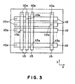
- Contact holes 110a, 110a, ... are formed in the passivation film 110 for connection to the wirings of decoder outputs for the memory section, the contact holes 110a, 110a, ... being disposed as shown in Fig. 3 substantially in an L-character shape.
- first metals (or semiconductor layers) 112, 112, ... are deposited in parallel with each other as shown in Fig. 3 while being connected to the wiring material 109 via the contact holes 110a, 110a, ....
- a passivation film 113 is deposited over the whole surface of the first metals 112 and passivation film 110.
- Contact holes 113a, 113a, ... are formed in the passivation film 113 above the first wirings 112 in accordance with the information to be written in ROMs.
- the contact holes are selectively formed at optional virtual or apparent intersections (three-dimensional intersections as viewed in the direction perpendicular to the X-Y surface) between the first and second metals 112 and 115.
- the second metals (or semiconductor layers) 115, 115, ... are deposited and patterned to be perpendicular to the first wirings as seen from Fig. 3.
- the end portions of the second metals are connected to the decoder outputs via the contact holes 110a, 110a, ....
- the interface at which the first and second metals (or semiconductor layers) contact each other within the contact holes 113a is formed with a p-n junction or Schottky junction so as to present a rectification function.
- the semiconductor device constructed as above operates as described in the following. Namely, the transistor type functional elements (data processing section) formed on the surface of the semiconductor substrate 100 perform information processing. Fixed information is being stored in the memory cell array formed above the transistor type functional elements, and is read when necessary.
- the data processing section and the peripheral circuit of the memory section have been formed on the surface of the semiconductor substrate 100.
- Other memories such as RAMs also may be formed on the surface of the substrate 100.
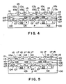
- FIG. 4 shows a semiconductor device functioning as a PROM.
- contact holes 113a have been formed at the virtual intersections (three-dimensional intersections) between the first and second metals (or semiconductor layers) in accordance with information to be stored.
- blind holes 113b, 113b are formed at all virtual intersections as shown in Fig. 4 while thin insulating films 113c, 113c, ... are interposed between two metals 112 and 115.
- holes 113b are first formed to extend completely to the first metal 112, and then an insulating film is deposited over the whole surface of the semiconductor device.
- the surface of the first metal 112, exposed to the holes 113b, may be oxidized.
- the thin insulating films 113c, 113c are selectively destroyed for example by applying a high voltage pulse (10 MV/cm). It is therefore possible for a user to write a desired program into a finished semiconductor device, thereby realizing a so-called PROM type semiconductor device.
- FIG. 5 shows a semiconductor device functioning as an EEPROM.
- a PROM type semiconductor device has been realized by forming a thin insulating film 113c at the virtual intersections between the first and second metals (or semiconductor layers) 112 and 115.
- ferroelectric members 117, 117, ... are formed in holes 113d, 113d, ... at virtual intersections.
- a ferroelectric member 117 may be deposited over the whole area of the semiconductor device inclusive of the holes 113d, and thereafter the film is etched back. Or other suitable methods may be used.
- barium titanate (BaTiO3), lead titanate zirconate (PZT: PbTiO3-PbZrO3) or the like may be used.
- a high voltage is selectively applied to the intersections to thereby change the polarization direction of the ferroelectric member 117 and store information.
- the semiconductor device shown in Fig. 5 functions as a non-volatile RAM (EEPROM).
Abstract
Description
- The present invention relates to a semiconductor device formed on a semiconductor substrate, and more particularly to a semiconductor device wherein elements for processing information and elements for storing information are formed on a single semiconductor substrate.
- With recent developments in semiconductor technology, a semiconductor device have been practically realized which has a great number of functional elements formed on a single semiconductor substrate. For example, there has been realized a semiconductor device having within its semiconductor substrate a CPU (Central Processing Unit) for performing logical operations, data control and the like, a ROM (Read Only Memory) for storing fixed data such as operating system (OS) and the like, a RAM (Random Access Memory) for storing temporary data, and other elements. Such a semiconductor device includes almost all functional elements necessary for a computer in one chip. A very compact device with great information processing capability is thus realized and has wide application to such as IC cards.
- Such a semiconductor device has been desired to have a more sophisticated function as its memory capacity increases and its logical circuits become large scaled. The reason for this is that devices which can process more information at higher speeds are becoming necessary. In order to meet such requirements, it is necessary to integrate elements as much as possible on a single semiconductor substrate. It therefore becomes necessary to make each element smaller. If not possible, the chip area will increase to pose a number of problems associated with manufacturing techniques, resulting in a difficulty in mass-producing devices of low cost.
- In order to make an element small, a precise control of lithography should be ensured and measures to count a degradation of reliability to be caused by miniaturization should be taken, thereby resulting in a difficulty associated with manufacturing techniques.
- The present invention has been made in consideration of the above problems. It is an object of the present invention to provide a semiconductor device having both a large memory capacity and a highly sophisticated information processing capability and being formed on a single semiconductor substrate without any increase of the chip area and without the need of severe miniaturization of elements.
- There are laminated, as an upper layer and lower layer on a single semiconductor substrate, a first functional block for data processing and a memory cell array of a second functional block for storage of various information necessary for the data processing. The overall dimensions of the semiconductor device can be made small when compared with a device which forms both the first and second functional blocks on the same surface. The miniaturization of the semiconductor device can be achieved without reducing the size of each of semiconductor elements constituting the first and second functional blocks small. There is no need therefore to miniaturize each semiconductor element, and hence there is no fear of lowering the reliability which might be caused by miniaturization.
- According to the present invention, the information necessary for the data processing by the first functional block is previously stored in the memory cell array.
- According to the present invention, virtual intersections (three-dimensional intersections) between conductive wires in the X- and Y-directions are optionally made conductive, or the state of ferroelectric members at virtual intersections is optionally changed. Accordingly, the information necessary for the data processing by the first functional block can be previously stored in the memory cell array of the second functional block. In other words, the information necessary for a particular user of this device can be previously stored in the memory cell array.
- According to the present invention, the overall dimensions of a semiconductor device can be made small without reducing the size of each semiconductor element small. In addition, since it is not necessary to make each element small, the difficulty in manufacturing is not increased, thereby not only allowing devices of low cost but also presenting no fear of lowering the reliability which might be caused through miniaturization. Furthermore, the memory capacity can be increased and the data processing functions can be highly sophisticated assuming that a device having the same dimensions as a conventional one is used.
- According to the present invention, the information necessary for the data processing can be previously stored in the memory cell array.
- According to the present invention, a user can optionally store in the memory cell the information necessary for the data processing, and in addition, information once stored can be rewritten.
-
- Fig. 1 is a schematic view illustrating the concept of the present invention;
- Figs. 2A to 2C are cross sections illustrating the manufacturing processes of a semiconductor device according to an embodiment of the present invention;
- Fig. 3 is a schematic view illustrating first and second wirings shown in Fig. 2C; and
- Figs. 4 and 5 are cross sections of semiconductor devices according to other embodiments of this invention.
-
- The embodiments of the present invention will be described with reference to the accompanying drawings.
- Fig. 1 is a schematic view illustrating the concept of the present invention. As seen from Fig. 1, the embodiment semiconductor device has a lower layer 200 and an
upper layer 300 laminated one upon the other on asemiconductor substrate 100. The lower layer 200 includes a first functional block (data processing section) and a part (constructed of transistors) of a second functional block (memory section). Theupper layer 300 includes the remaining part (not including transistors) of the second functional block. The first functional block has a function of performing logical operations, data control and the like, and is shown as a CPU 202 in Fig. 1. The second functional block is used for storing information, a part of the first functional block being shown in Fig. 1 as amemory cell array 302 of ROM in theupper layer 300 and aRAM 204 and a peripheral circuit (decoder, control unit, input/output unit and the like) 206 of ROM in the lower layer 200. - Figs. 2A to 2C are cross sections illustrating the manufacturing processes of a semiconductor device according to the first embodiment which is an example of the device conceptually shown in Fig. 1.
- The first embodiment operates as a mask ROM. As shown in Fig. 2A, there are formed on a semiconductor substrate (P-type silicon substrate) 100 an N-
channel transistor 101 and P-channel transistor 102 as the data processing section.Reference numeral 103 represents an N-type well provided for the P-channel transistor 102. There are also formed on the surface of thesilicon substrate 100 an N-channel transistor 104 and a P-channel transistor 105 which constitute the peripheral circuit of the memory section, e.g., a decoder, control unit, input/output unit and the like.Reference numeral 106 represents an N-type well provided for the P-channel transistor 105. These elements are electrically isolated from each other byfield oxide Reference numeral 108 represents a passivation film deposited for protecting the elements, the passivation film being made of SiO₂ or PSG formed by a CVD method. Contactholes passivation film 108 where necessary, andwiring material 109 is provided within the holes for interconnection between elements. - Next, as shown in Fig. 2B, a
passivation film 110 is deposited on thepassivation film 108 andwiring material 109. Contactholes passivation film 110 for connection to the wirings of decoder outputs for the memory section, thecontact holes wiring material 109 via thecontact holes - Next, as shown in Fig. 2C, a
passivation film 113 is deposited over the whole surface of thefirst metals 112 andpassivation film 110. Contactholes passivation film 113 above thefirst wirings 112 in accordance with the information to be written in ROMs. As seen from Fig. 3, the contact holes are selectively formed at optional virtual or apparent intersections (three-dimensional intersections as viewed in the direction perpendicular to the X-Y surface) between the first andsecond metals contact holes contact holes 113a is formed with a p-n junction or Schottky junction so as to present a rectification function. - The semiconductor device constructed as above operates as described in the following. Namely, the transistor type functional elements (data processing section) formed on the surface of the
semiconductor substrate 100 perform information processing. Fixed information is being stored in the memory cell array formed above the transistor type functional elements, and is read when necessary. - As seen from Fig. 2C, without increasing the chip area, it is possible to realize a semiconductor device having a highly sophisticated information processing capability and a large memory capacity.
- In the above embodiment, the data processing section and the peripheral circuit of the memory section have been formed on the surface of the
semiconductor substrate 100. Other memories such as RAMs also may be formed on the surface of thesubstrate 100. - Another embodiment will be described with reference to Fig. 4 which shows a semiconductor device functioning as a PROM. In the first embodiment shown in Figs. 2A to 2C,
contact holes 113a have been formed at the virtual intersections (three-dimensional intersections) between the first and second metals (or semiconductor layers) in accordance with information to be stored. In the second embodiment shown in Fig. 4,blind holes films metals - In order to form such blind holes, there are many practical methods. For example, holes 113b are first formed to extend completely to the
first metal 112, and then an insulating film is deposited over the whole surface of the semiconductor device. Alternatively, the surface of thefirst metal 112, exposed to theholes 113b, may be oxidized. - In writing information into the semiconductor device shown in Fig. 4, the thin insulating
films - A further embodiment of this invention will be described with reference to Fig. 5 which shows a semiconductor device functioning as an EEPROM. In the embodiment shown in Fig. 4, a PROM type semiconductor device has been realized by forming a thin
insulating film 113c at the virtual intersections between the first and second metals (or semiconductor layers) 112 and 115. In the embodiment shown in Fig. 5,ferroelectric members holes ferroelectric member 117 may be deposited over the whole area of the semiconductor device inclusive of theholes 113d, and thereafter the film is etched back. Or other suitable methods may be used. As theferroelectric member 117, barium titanate (BaTiO₃), lead titanate zirconate (PZT: PbTiO₃-PbZrO₃) or the like may be used. - In the semiconductor device shown in Fig. 5, a high voltage is selectively applied to the intersections to thereby change the polarization direction of the
ferroelectric member 117 and store information. In other words, the semiconductor device shown in Fig. 5 functions as a non-volatile RAM (EEPROM). - Reference signs in the claims are intended for better understanding and shall not limit the scope.
Claims (10)
a semiconductor substrate (100);
a first functional block (202) formed directly on said semiconductor substrate (100) for performing data processing;
a second functional block (206, 302) for previously storing information necessary for performing said data processing, said second functional block including a memory cell array (302) having a plurality of memory cells and a functional element section (206) at least for reading data from said memory cell array,
said functional element section being formed directly on said semiconductor substrate, and said memory cell array being formed above said first functional block and functional element section with an insulating passivation film (110) interposed therebetween.
Priority Applications (1)
| Application Number | Priority Date | Filing Date | Title |
|---|---|---|---|
| EP02001974A EP1215727A3 (en) | 1989-03-14 | 1990-03-14 | Semiconductor structure for processing and storing of information |
Applications Claiming Priority (2)
| Application Number | Priority Date | Filing Date | Title |
|---|---|---|---|
| JP61559/89 | 1989-03-14 | ||
| JP1061559A JP2778977B2 (en) | 1989-03-14 | 1989-03-14 | Semiconductor device and manufacturing method thereof |
Related Child Applications (1)
| Application Number | Title | Priority Date | Filing Date |
|---|---|---|---|
| EP02001974A Division EP1215727A3 (en) | 1989-03-14 | 1990-03-14 | Semiconductor structure for processing and storing of information |
Publications (2)
| Publication Number | Publication Date |
|---|---|
| EP0387834A2 true EP0387834A2 (en) | 1990-09-19 |
| EP0387834A3 EP0387834A3 (en) | 1991-07-24 |
Family
ID=13174590
Family Applications (2)
| Application Number | Title | Priority Date | Filing Date |
|---|---|---|---|
| EP02001974A Withdrawn EP1215727A3 (en) | 1989-03-14 | 1990-03-14 | Semiconductor structure for processing and storing of information |
| EP19900104813 Ceased EP0387834A3 (en) | 1989-03-14 | 1990-03-14 | Semiconductor structure for processing and storing of information |
Family Applications Before (1)
| Application Number | Title | Priority Date | Filing Date |
|---|---|---|---|
| EP02001974A Withdrawn EP1215727A3 (en) | 1989-03-14 | 1990-03-14 | Semiconductor structure for processing and storing of information |
Country Status (4)
| Country | Link |
|---|---|
| US (1) | US5521417A (en) |
| EP (2) | EP1215727A3 (en) |
| JP (1) | JP2778977B2 (en) |
| KR (1) | KR930002285B1 (en) |
Cited By (14)
| Publication number | Priority date | Publication date | Assignee | Title |
|---|---|---|---|---|
| EP0707316A3 (en) * | 1994-10-11 | 1998-08-26 | Matsushita Electric Industrial Co., Ltd. | Semiconducteur device and method for fabricating the same, memory core chip and memory peripheral circuit chip |
| WO2002043067A2 (en) * | 2000-11-23 | 2002-05-30 | Infineon Technologies Ag | Integrated memory with an arrangement of non-volatile memory cells and method for the production and operation of an integrated memory |
| US6483736B2 (en) | 1998-11-16 | 2002-11-19 | Matrix Semiconductor, Inc. | Vertically stacked field programmable nonvolatile memory and method of fabrication |
| US6525953B1 (en) | 2001-08-13 | 2003-02-25 | Matrix Semiconductor, Inc. | Vertically-stacked, field-programmable, nonvolatile memory and method of fabrication |
| US6593624B2 (en) | 2001-09-25 | 2003-07-15 | Matrix Semiconductor, Inc. | Thin film transistors with vertically offset drain regions |
| US6624485B2 (en) | 2001-11-05 | 2003-09-23 | Matrix Semiconductor, Inc. | Three-dimensional, mask-programmed read only memory |
| US6731011B2 (en) | 2002-02-19 | 2004-05-04 | Matrix Semiconductor, Inc. | Memory module having interconnected and stacked integrated circuits |
| US6737675B2 (en) | 2002-06-27 | 2004-05-18 | Matrix Semiconductor, Inc. | High density 3D rail stack arrays |
| US6843421B2 (en) | 2001-08-13 | 2005-01-18 | Matrix Semiconductor, Inc. | Molded memory module and method of making the module absent a substrate support |
| US7352199B2 (en) | 2001-02-20 | 2008-04-01 | Sandisk Corporation | Memory card with enhanced testability and methods of making and using the same |
| EP2037461A2 (en) * | 2007-09-12 | 2009-03-18 | Samsung Electronics Co., Ltd. | Multi-layered memory devices |
| US7655509B2 (en) | 2002-03-13 | 2010-02-02 | Sandisk 3D Llc | Silicide-silicon oxide-semiconductor antifuse device and method of making |
| US7825455B2 (en) | 2000-08-14 | 2010-11-02 | Sandisk 3D Llc | Three terminal nonvolatile memory device with vertical gated diode |
| US9478495B1 (en) | 2015-10-26 | 2016-10-25 | Sandisk Technologies Llc | Three dimensional memory device containing aluminum source contact via structure and method of making thereof |
Families Citing this family (21)
| Publication number | Priority date | Publication date | Assignee | Title |
|---|---|---|---|---|
| JPH11505323A (en) * | 1995-04-18 | 1999-05-18 | カーティス インスツルメンツ インコーポレイテッド | Small and low-priced semiconductor equipment |
| US5874340A (en) * | 1996-07-17 | 1999-02-23 | Advanced Micro Devices, Inc. | Method for fabrication of a non-symmetrical transistor with sequentially formed gate electrode sidewalls |
| US5877050A (en) * | 1996-09-03 | 1999-03-02 | Advanced Micro Devices, Inc. | Method of making N-channel and P-channel devices using two tube anneals and two rapid thermal anneals |
| US6051471A (en) * | 1996-09-03 | 2000-04-18 | Advanced Micro Devices, Inc. | Method for making asymmetrical N-channel and symmetrical P-channel devices |
| US5648286A (en) * | 1996-09-03 | 1997-07-15 | Advanced Micro Devices, Inc. | Method of making asymmetrical transistor with lightly doped drain region, heavily doped source and drain regions, and ultra-heavily doped source region |
| US5677224A (en) * | 1996-09-03 | 1997-10-14 | Advanced Micro Devices, Inc. | Method of making asymmetrical N-channel and P-channel devices |
| US5890199A (en) * | 1996-10-21 | 1999-03-30 | Ramtron International Corporation | Data processor incorporating a ferroelectric memory array selectably configurable as read/write and read only memory |
| US6027978A (en) * | 1997-01-28 | 2000-02-22 | Advanced Micro Devices, Inc. | Method of making an IGFET with a non-uniform lateral doping profile in the channel region |
| US5849622A (en) * | 1997-03-07 | 1998-12-15 | Advanced Micro Devices, Inc. | Method of forming a source implant at a contact masking step of a process flow |
| US5915167A (en) * | 1997-04-04 | 1999-06-22 | Elm Technology Corporation | Three dimensional structure memory |
| US5923982A (en) * | 1997-04-21 | 1999-07-13 | Advanced Micro Devices, Inc. | Method of making asymmetrical transistor with lightly and heavily doped drain regions and ultra-heavily doped source region using two source/drain implant steps |
| US6004849A (en) * | 1997-08-15 | 1999-12-21 | Advanced Micro Devices, Inc. | Method of making an asymmetrical IGFET with a silicide contact on the drain without a silicide contact on the source |
| US5904529A (en) * | 1997-08-25 | 1999-05-18 | Advanced Micro Devices, Inc. | Method of making an asymmetrical IGFET and providing a field dielectric between active regions of a semiconductor substrate |
| US6096588A (en) * | 1997-11-01 | 2000-08-01 | Advanced Micro Devices, Inc. | Method of making transistor with selectively doped channel region for threshold voltage control |
| TW587252B (en) * | 2000-01-18 | 2004-05-11 | Hitachi Ltd | Semiconductor memory device and data processing device |
| US8575719B2 (en) | 2000-04-28 | 2013-11-05 | Sandisk 3D Llc | Silicon nitride antifuse for use in diode-antifuse memory arrays |
| KR20050104652A (en) * | 2004-04-29 | 2005-11-03 | 삼성에스디아이 주식회사 | Electron emission display device and driving method thereof |
| EP2669504A1 (en) | 2012-05-30 | 2013-12-04 | Caterpillar Motoren GmbH & Co. KG | Plunger for an internal combustion engine fuel pump |
| EP2672101A1 (en) | 2012-06-05 | 2013-12-11 | Caterpillar Motoren GmbH & Co. KG | Injection nozzle |
| WO2013182213A1 (en) | 2012-06-05 | 2013-12-12 | Caterpillar Motoren Gmbh & Co. Kg | Fuel guiding component |
| CN107301222B (en) * | 2016-03-07 | 2020-11-10 | 杭州海存信息技术有限公司 | Big data memory with data analysis function |
Citations (2)
| Publication number | Priority date | Publication date | Assignee | Title |
|---|---|---|---|---|
| EP0075945A2 (en) * | 1981-09-30 | 1983-04-06 | Kabushiki Kaisha Toshiba | Stacked semiconductor device and method for manufacturing the device |
| WO1986004447A1 (en) * | 1985-01-29 | 1986-07-31 | Ramtron Corporation | Method of making an integrated ferroelectric device, and device produced thereby |
Family Cites Families (11)
| Publication number | Priority date | Publication date | Assignee | Title |
|---|---|---|---|---|
| US2905928A (en) * | 1955-09-08 | 1959-09-22 | Bell Telephone Labor Inc | Ferroelectric storage array |
| JPS5858809B2 (en) * | 1976-02-28 | 1983-12-27 | 富士通株式会社 | Manufacturing method of semiconductor device |
| US4149301A (en) * | 1977-07-25 | 1979-04-17 | Ferrosil Corporation | Monolithic semiconductor integrated circuit-ferroelectric memory drive |
| US4233671A (en) * | 1979-01-05 | 1980-11-11 | Stanford University | Read only memory and integrated circuit and method of programming by laser means |
| US4458297A (en) * | 1981-01-16 | 1984-07-03 | Mosaic Systems, Inc. | Universal interconnection substrate |
| US4424579A (en) * | 1981-02-23 | 1984-01-03 | Burroughs Corporation | Mask programmable read-only memory stacked above a semiconductor substrate |
| JPS5837948A (en) * | 1981-08-31 | 1983-03-05 | Toshiba Corp | Laminated semiconductor memory device |
| JPS5846680A (en) * | 1981-09-14 | 1983-03-18 | Fujitsu Ltd | Memory element |
| JPH0616530B2 (en) * | 1985-02-28 | 1994-03-02 | 株式会社東芝 | Semiconductor integrated circuit |
| US4823181A (en) * | 1986-05-09 | 1989-04-18 | Actel Corporation | Programmable low impedance anti-fuse element |
| US4888630A (en) * | 1988-03-21 | 1989-12-19 | Texas Instruments Incorporated | Floating-gate transistor with a non-linear intergate dielectric |
-
1989
- 1989-03-14 JP JP1061559A patent/JP2778977B2/en not_active Expired - Lifetime
-
1990
- 1990-03-14 EP EP02001974A patent/EP1215727A3/en not_active Withdrawn
- 1990-03-14 KR KR1019900003421A patent/KR930002285B1/en not_active IP Right Cessation
- 1990-03-14 EP EP19900104813 patent/EP0387834A3/en not_active Ceased
-
1993
- 1993-01-19 US US08/332,377 patent/US5521417A/en not_active Expired - Lifetime
Patent Citations (2)
| Publication number | Priority date | Publication date | Assignee | Title |
|---|---|---|---|---|
| EP0075945A2 (en) * | 1981-09-30 | 1983-04-06 | Kabushiki Kaisha Toshiba | Stacked semiconductor device and method for manufacturing the device |
| WO1986004447A1 (en) * | 1985-01-29 | 1986-07-31 | Ramtron Corporation | Method of making an integrated ferroelectric device, and device produced thereby |
Non-Patent Citations (2)
| Title |
|---|
| ELECTRONIC ENGINEERING vol. 60, no. 737, May 1988, pages 33-41, Woolwich, London, GB; "Technology Focus Memory Devices" * |
| FGCS - FUTURE, GENERATION, COMPUTER, SYSTEMS vol. 4, no. 2, September 1988, pages 145-155, Amsterdam, NL; T. KUROKAWA et al.: "3-D VLSI Technology in Japan and an Example: a Syndrome Decoder for Double Error Correction" * |
Cited By (31)
| Publication number | Priority date | Publication date | Assignee | Title |
|---|---|---|---|---|
| EP0707316A3 (en) * | 1994-10-11 | 1998-08-26 | Matsushita Electric Industrial Co., Ltd. | Semiconducteur device and method for fabricating the same, memory core chip and memory peripheral circuit chip |
| US6064585A (en) * | 1994-10-11 | 2000-05-16 | Matsushita Electric Industrial Co. | Semiconductor device and method for fabricating the same, memory core chip and memory peripheral circuit chip |
| US6313493B1 (en) | 1994-10-11 | 2001-11-06 | Matsushita Electric Industrial Co., Ltd. | Semiconductor device and method for fabricating the same, memory core chip and memory peripheral circuit chip |
| EP1154434A1 (en) * | 1994-10-11 | 2001-11-14 | Matsushita Electric Industrial Co., Ltd. | Semiconductor device and method for fabricating the same, memory core chip and memory peripheral circuit chip |
| EP1376593A1 (en) * | 1994-10-11 | 2004-01-02 | Matsushita Electric Industrial Co., Ltd. | Semiconductor device and method for fabricating the same, memory core chip and memory peripheral circuit chip |
| US6483736B2 (en) | 1998-11-16 | 2002-11-19 | Matrix Semiconductor, Inc. | Vertically stacked field programmable nonvolatile memory and method of fabrication |
| US6780711B2 (en) | 1998-11-16 | 2004-08-24 | Matrix Semiconductor, Inc | Vertically stacked field programmable nonvolatile memory and method of fabrication |
| US7978492B2 (en) | 1998-11-16 | 2011-07-12 | Sandisk 3D Llc | Integrated circuit incorporating decoders disposed beneath memory arrays |
| US9171857B2 (en) | 2000-08-14 | 2015-10-27 | Sandisk 3D Llc | Dense arrays and charge storage devices |
| US10008511B2 (en) | 2000-08-14 | 2018-06-26 | Sandisk Technologies Llc | Dense arrays and charge storage devices |
| US9559110B2 (en) | 2000-08-14 | 2017-01-31 | Sandisk Technologies Llc | Dense arrays and charge storage devices |
| US8981457B2 (en) | 2000-08-14 | 2015-03-17 | Sandisk 3D Llc | Dense arrays and charge storage devices |
| US10644021B2 (en) | 2000-08-14 | 2020-05-05 | Sandisk Technologies Llc | Dense arrays and charge storage devices |
| US8853765B2 (en) | 2000-08-14 | 2014-10-07 | Sandisk 3D Llc | Dense arrays and charge storage devices |
| US8823076B2 (en) | 2000-08-14 | 2014-09-02 | Sandisk 3D Llc | Dense arrays and charge storage devices |
| US7825455B2 (en) | 2000-08-14 | 2010-11-02 | Sandisk 3D Llc | Three terminal nonvolatile memory device with vertical gated diode |
| WO2002043067A2 (en) * | 2000-11-23 | 2002-05-30 | Infineon Technologies Ag | Integrated memory with an arrangement of non-volatile memory cells and method for the production and operation of an integrated memory |
| WO2002043067A3 (en) * | 2000-11-23 | 2002-12-05 | Infineon Technologies Ag | Integrated memory with an arrangement of non-volatile memory cells and method for the production and operation of an integrated memory |
| US6798689B2 (en) | 2000-11-23 | 2004-09-28 | Infineon Technologies Ag | Integrated memory with a configuration of non-volatile memory cells and method for fabricating and for operating the integrated memory |
| US7352199B2 (en) | 2001-02-20 | 2008-04-01 | Sandisk Corporation | Memory card with enhanced testability and methods of making and using the same |
| US6525953B1 (en) | 2001-08-13 | 2003-02-25 | Matrix Semiconductor, Inc. | Vertically-stacked, field-programmable, nonvolatile memory and method of fabrication |
| US6843421B2 (en) | 2001-08-13 | 2005-01-18 | Matrix Semiconductor, Inc. | Molded memory module and method of making the module absent a substrate support |
| US6689644B2 (en) | 2001-08-13 | 2004-02-10 | Matrix Semiconductor, Inc. | Vertically-stacked, field-programmable, nonvolatile memory and method of fabrication |
| US6593624B2 (en) | 2001-09-25 | 2003-07-15 | Matrix Semiconductor, Inc. | Thin film transistors with vertically offset drain regions |
| US6624485B2 (en) | 2001-11-05 | 2003-09-23 | Matrix Semiconductor, Inc. | Three-dimensional, mask-programmed read only memory |
| US6731011B2 (en) | 2002-02-19 | 2004-05-04 | Matrix Semiconductor, Inc. | Memory module having interconnected and stacked integrated circuits |
| US7915095B2 (en) | 2002-03-13 | 2011-03-29 | Sandisk 3D Llc | Silicide-silicon oxide-semiconductor antifuse device and method of making |
| US7655509B2 (en) | 2002-03-13 | 2010-02-02 | Sandisk 3D Llc | Silicide-silicon oxide-semiconductor antifuse device and method of making |
| US6737675B2 (en) | 2002-06-27 | 2004-05-18 | Matrix Semiconductor, Inc. | High density 3D rail stack arrays |
| EP2037461A2 (en) * | 2007-09-12 | 2009-03-18 | Samsung Electronics Co., Ltd. | Multi-layered memory devices |
| US9478495B1 (en) | 2015-10-26 | 2016-10-25 | Sandisk Technologies Llc | Three dimensional memory device containing aluminum source contact via structure and method of making thereof |
Also Published As
| Publication number | Publication date |
|---|---|
| KR900015326A (en) | 1990-10-26 |
| EP1215727A2 (en) | 2002-06-19 |
| KR930002285B1 (en) | 1993-03-29 |
| US5521417A (en) | 1996-05-28 |
| EP1215727A3 (en) | 2007-05-02 |
| JP2778977B2 (en) | 1998-07-23 |
| EP0387834A3 (en) | 1991-07-24 |
| JPH02239652A (en) | 1990-09-21 |
Similar Documents
| Publication | Publication Date | Title |
|---|---|---|
| EP0387834A2 (en) | Semiconductor structure for processing and storing of information | |
| US5909624A (en) | Method of making integration of high value capacitor with ferroelectric memory | |
| EP1154434B1 (en) | Method for fabricating a semiconductor device | |
| JPH07120719B2 (en) | Semiconductor memory device | |
| JP2508288B2 (en) | Semiconductor memory device | |
| KR950034801A (en) | Memory | |
| JP3780003B2 (en) | Semiconductor integrated circuit device | |
| EP3958319B1 (en) | Memory, forming method therefor and control method therefor | |
| JPH0661452A (en) | Semiconductor device | |
| EP0650196A2 (en) | Semiconductor integrated circuit device and method of producing the same using master slice approach | |
| US11443780B2 (en) | Vertical access line multiplexor | |
| JPH0724298B2 (en) | Semiconductor memory device | |
| JP3179368B2 (en) | Static memory cell | |
| JPH01200661A (en) | Dynamic type semiconductor storage device | |
| US10777564B2 (en) | Non-volatile memory device | |
| JP3048963B2 (en) | Semiconductor memory device | |
| US4494218A (en) | Read only memory using series connected depletion transistors as bus lines | |
| JP2563803B2 (en) | Semiconductor memory device | |
| JPH01128563A (en) | Semiconductor memory | |
| JPH05167044A (en) | Semiconductor nonvolatile memory device and its write method | |
| JPH0336762A (en) | Semiconductor memory device | |
| JP3048496B2 (en) | Semiconductor device | |
| JPH07307446A (en) | Semiconductor device | |
| CN117858497A (en) | Memory, manufacturing method thereof and memory system | |
| JPH04186671A (en) | Semiconductor memory |
Legal Events
| Date | Code | Title | Description |
|---|---|---|---|
| PUAI | Public reference made under article 153(3) epc to a published international application that has entered the european phase |
Free format text: ORIGINAL CODE: 0009012 |
|
| 17P | Request for examination filed |
Effective date: 19900314 |
|
| AK | Designated contracting states |
Kind code of ref document: A2 Designated state(s): DE FR GB |
|
| PUAL | Search report despatched |
Free format text: ORIGINAL CODE: 0009013 |
|
| RHK1 | Main classification (correction) |
Ipc: H01L 27/06 |
|
| AK | Designated contracting states |
Kind code of ref document: A3 Designated state(s): DE FR GB |
|
| 17Q | First examination report despatched |
Effective date: 19930614 |
|
| APAB | Appeal dossier modified |
Free format text: ORIGINAL CODE: EPIDOS NOAPE |
|
| APAB | Appeal dossier modified |
Free format text: ORIGINAL CODE: EPIDOS NOAPE |
|
| APAD | Appeal reference recorded |
Free format text: ORIGINAL CODE: EPIDOS REFNE |
|
| APAD | Appeal reference recorded |
Free format text: ORIGINAL CODE: EPIDOS REFNE |
|
| APAB | Appeal dossier modified |
Free format text: ORIGINAL CODE: EPIDOS NOAPE |
|
| APAB | Appeal dossier modified |
Free format text: ORIGINAL CODE: EPIDOS NOAPE |
|
| STAA | Information on the status of an ep patent application or granted ep patent |
Free format text: STATUS: THE APPLICATION HAS BEEN REFUSED |
|
| 18R | Application refused |
Effective date: 20020405 |
|
| APAF | Appeal reference modified |
Free format text: ORIGINAL CODE: EPIDOSCREFNE |