EP0374906B1 - Synchronization recovery circuit for recovering word synchronization and radiocommunication apparatus using the same - Google Patents
Synchronization recovery circuit for recovering word synchronization and radiocommunication apparatus using the same Download PDFInfo
- Publication number
- EP0374906B1 EP0374906B1 EP89123599A EP89123599A EP0374906B1 EP 0374906 B1 EP0374906 B1 EP 0374906B1 EP 89123599 A EP89123599 A EP 89123599A EP 89123599 A EP89123599 A EP 89123599A EP 0374906 B1 EP0374906 B1 EP 0374906B1
- Authority
- EP
- European Patent Office
- Prior art keywords
- data
- synchronization
- parallel
- serial
- bit
- Prior art date
- Legal status (The legal status is an assumption and is not a legal conclusion. Google has not performed a legal analysis and makes no representation as to the accuracy of the status listed.)
- Expired - Lifetime
Links
Images


Classifications
-
- H—ELECTRICITY
- H04—ELECTRIC COMMUNICATION TECHNIQUE
- H04L—TRANSMISSION OF DIGITAL INFORMATION, e.g. TELEGRAPHIC COMMUNICATION
- H04L7/00—Arrangements for synchronising receiver with transmitter
- H04L7/04—Speed or phase control by synchronisation signals
- H04L7/041—Speed or phase control by synchronisation signals using special codes as synchronising signal
- H04L7/042—Detectors therefor, e.g. correlators, state machines
-
- H—ELECTRICITY
- H04—ELECTRIC COMMUNICATION TECHNIQUE
- H04L—TRANSMISSION OF DIGITAL INFORMATION, e.g. TELEGRAPHIC COMMUNICATION
- H04L7/00—Arrangements for synchronising receiver with transmitter
- H04L7/04—Speed or phase control by synchronisation signals
- H04L7/041—Speed or phase control by synchronisation signals using special codes as synchronising signal
- H04L7/046—Speed or phase control by synchronisation signals using special codes as synchronising signal using a dotting sequence
Definitions
- the present invention generally relates to synchronization recovery circuits and radiocommunication apparatuses using such circuits, and more particularly, to a synchronization recovery circuit which detects a word synchronizing character in a received data signal for recovering word synchronization in a cellular-type communication system, and to a radiocommunication apparatus such as car telephone and portable telephone using such a synchronization recovery circuit.
- a cellular-type communication system has been widely utilized in the form of a mobile radio telephone such as car telephone or portable telephone.
- a cellular-type communication system an area to be covered is divided into multiple cells, each of which is provided with a radio base station and assigned a group of channels.
- Such a small-sized service area of each cell and reduced transmission output of a base station enable frequent reuse of the frequencies, admitting an increased number of subscribers.
- Each radio base station has two types of radio channels, one of which is a bidirectional control channel for such several kinds of digital control as mentioned above, and the other is a bidirectional audio channel for conversation over the telephone.
- the control channel comprises a forward control channel (FOCC) used for communication from a radio base station to a mobile station and a reverse control channel (RECC) used for communication from a mobile station to a radio base station, which are generally used for control of every kind before the audio channel is established, and not for conversation.
- the audio channel comprises a forward audio channel (FVC) used for communication from a radio base station to a mobile station and a reverse audio channel (RVC) used for communication from a mobile station to a radio base station.
- FVC forward audio channel
- RVC reverse audio channel
- a radiocommunication apparatus of a mobile station is first required to detect the word synchronizing character out of a received data signal for recovering word synchronization.
- a radiocommunication apparatus as disclosed in the US Patent No. 4,029,900, there is provided a synchronization recovery circuit which detects the word synchronizing character out of the data signal for recovering word synchronization.
- the word synchronization is recovered by supplying a control circuit for data processing with a word synchronizing signal which has been generated based on the detected word synchronizing character.
- the conventional synchronization recovery circuit is constituted in the light of its hardware construction such that the word synchronizing signal is serially applied to the control circuit. Therefore, in order to recover word synchronization based on such a serial word synchronizing signal, also the data signal must be serially applied to the control circuit.
- the control circuit receives both of the word synchronizing signal and the data signal serially and accepts the data signal as effective data for use, only after a word synchronizing position is identified.
- data may possibly drop out due to high data transmitting rate of the celluar-type communication system.
- control circuit is always required to access the data signal and thus can not do any other processing such as key scan, LCD display, AF (Analog Frequency) processing, radio-functional processing or the like during the access, prevented from performing any kind of processing required as a mobile station, at a higher speed.
- any other processing such as key scan, LCD display, AF (Analog Frequency) processing, radio-functional processing or the like during the access, prevented from performing any kind of processing required as a mobile station, at a higher speed.
- EP-A-0 052 432 discloses an apparatus for extracting synchronizing information from an incoming serial-bit digital television signal according to the precharacterizing portion of claim 1 or claim 13.
- the incoming serial-bit digital television signal is formed of a sequence of word blocks, each word block being formed of N n-bit words and each word block including a predetermined serial group of n-bits forming said synchronizing information.
- the apparatus further de-serializes the incoming digital signal in dependency of the synchronizing information.
- the control means in this apparatus are arranged only to perform synchronization recovery. An additional microprocessor must be provided for performing any other processing.
- WO 87/01490 discloses a radiotelephone system in which the signalling protocol for the system is embedded in the frame synchronization of the digital messages transmitted on the system.
- System state communication is achieved by utilizing a sequence of normal synchronization words and the corresponding inverses.
- Reliability of the coding is achieved by detecting normal or inverse words as binary levels when fewer than a predetermined number of bit errors exist in the bit sequence. If the predetermined number of bit errors is exceeded, a selected binary one or zero is substituted. This selected sequence of binary levels is decoded and the Hamming distance between a masked decoded sequence and a masked selected sequence is calculated. If the Hamming distance calculation yields a number greater than the error correction capability of the coding function, a new set of substituted binary levels is tried, otherwise the decoded sequence is accepted as correct.
- control means of this system are arranged so as to execute interruption processing in order to recover word synchronization and adapted to execute other processings than the word synchronization recovery except during the time in which said interruption processing is to be executed.
- Another pbject of the present invention is to enable word synchronization recovery of received data with parallel signal processing in a radiocommunication apparatus as a mobile station.
- the main advantage of the present invention is, therefore, that since the received data signal and the word synchronizing signal indicating the synchronizing position thereof are both processed as parallel data, the word synchronization can be quickly recovered and thus all the processings required from a radiocommunication apparatus can be done at a higher speed.
- Fig. 1 is a diagram showing a typical format of a forward control channel message.
- Figs. 2 (a) and (b) are diagrams showing specific examples of a bit synchronization field and a word synchronization field, respectively.
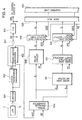
- Fig. 3 is a schematic block diagram showing a radiocommunication apparatus according to an embodiment of the present invention.
- Fig. 4 is a block diagram showing an internal structure of the data receiver in the radiocommunication apparatus shown in Fig. 3.
- Fig. 5 is a diagram showing details of the serial-parallel converter shown in Fig. 4.
- Fig. 6 is a block diagram showing details of the 8-bit shift register shown in Fig. 5.
- Fig. 7 is a block diagram showing details of the word synchronization detecting circuit and the word synchronization detecting shift register shown in Fig. 4.
- Fig. 8 is a block diagram showing details of the delaying circuit shown in Fig. 4.
- Fig. 9 is a block diagram showing details of the received data output port and the word synchronization detection output port shown in Fig. 4.
- Fig. 11 is a timing chart for explaining operation of the circuit shown in Fig. 4.
- Fig. 12 is a diagram for schematically explaining operation principles of the circuit shown in Fig. 4.
- Fig. 13 is a block diagram showing details of the control circuit shown in Fig. 3.
- Fig. 14 is a flow chart for explaining operation of the microcomputer shown in Fig. 13.
- Fig. 15 is a flow chart showing another example of processing by the microcomputer shown in Fig. 13.
- a forward control channel message (baseband data signal) is transmitted from a radio base station to a mobile station (radiocommunication apparatus), which will perform processings such as registration, channel change or the like according to the received message.
- Fig. 1 is a diagram showing a typical format of such a forward control channel message.
- This message is largely composited of a bit synchronization field, a word synchronization field and a data message. More particularly, the bit synchronization field is, as shown in Fig. 2 (a), a 10-bit field having alternate 1 and 0 bits recurrent in sequence (known as dotting).
- the word synchronization field in turn, as shown in Fig. 2 (b), is a 11-bit field having a bit arrangement which is rarely seen in the data message. In the United States, for example, the arrangement of "11100010010" as shown in Fig. 2 (b) is employed.
- one busy-idle bit is added to every 10 bits of the bit synchronization field, the word synchronization field and the respective data messages.
- This busy-idle bit serves to inform a mobile station of whether the transmission source of the message, or a radio base station is prepared to receive, or of vacancy status of the reverse control channel (RECC).
- the bit synchronization field, the word synchronization field and the data message are in practice comprised of 11 bits, 12 bits and 44 bits, respectively.
- the message shown in Fig. 1 will be then transferred, for example in the United States, at a 10 kilobit/second rate after Manchester-encoded in the well-known manner.
- Fig. 3 is a schematic block diagram of a radiocommunication apparatus as a mobile station in a cellular system according to an embodiment of the present invention.
- an antenna 3 is connected to a receiver 1 and a transmitter 2 through an antenna coupler 4.
- the receiver 1 FM-demodulates a received signal which has been received from a radio station with the antenna 3.
- the receiver 1 applies a data signal on the forward control channel to a data receiver 6 and a received audio signal on the forward audio channel to an audio processing circuit 5 by use of a discriminator not shown.
- the data receiver 6 detects a word synchronizing character out of the applied message of FOCC and applies a word synchronizing signal to a control circuit 8 constituted of a 8-bit microprocessor, along with the data signal.
- the control circuit 8 identifies a synchronizing position of the data signal, based on the applied word synchronizing signal, before executing any kind of control according to the data signal.
- the control circuit 8 performs additional processing and control necessary for a key matrix 11 or an LCD driver 12.
- the audio processing portion 5 amplifies the applied message of FVC for application to a handset speaker 10. This enables a user of a mobile station to receive a communication from another. Meanwhile, the control circuit 8 performs control such as muting instruction also for the audio processing circuit 5.
- the data transmitter 7 Manchester-encodes a data signal from the control circuit 8 for application to the transmitter 2 as a message for RECC. Meanwhile, the audio processing circuit 5 processes an audio signal applied from a user through a microphone 9 for application to the transmitter 2 as a transmitting audio signal for RVC. The transmitter 2 FM-modulates these signals for transmission to a base station by use of the antenna 3.
- FIG. 4 is a block diagram showing an internal structure of the data receiver 6 shown in Fig. 3, the respective parts of which are shown in the block diagrams of Figs. 5 to 10 in detail. Furthermore, Fig. 11 is a timing chart showing signals of the data receiver 6, and Fig. 12 is a diagram for schematically explaining operation principles thereof.
- a forward control channel message transmitted from a radio base station is FM-demodulated in the receiver 1 and extracted by an LPF 13.
- the analog forward control channel message extracted by the LPF 13 is digitalized by a limiter 601 before applied to a clock signal generating circuit 602 and a Manchester decoder 603 as a data signal in Manchester code format.
- the clock signal generating circuit 602 which is constituted of a well-known PLL (Phase Locked Loop) circuit generates a clock signal RT (Fig. 11(b)) which has been bit-synchronized with the data signal in Manchester code format.
- This clock signal RT is applied to the Manchester decoder 603 and an inverter 607, and also to a delaying circuit 608 and a word synchronization detecting shift register 621 as will be described later.
- the Manchester decoder 603 converts, in response to the data signal and the clock signal RT, the data signal from the Manchester code format to NRZ (Non Return to Zero) format (Fig. 11(a)) and applies the converted signal to a serial-parallel converter 604.
- This serial-parallel converter 604 has function of a 16-bit shift register and thus converts the serial NRZ data from the Manchester decoder 603 into parallel data of 16 bits.
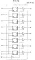
- Fig. 5 is a diagram showing a structure of the serial-parallel converter 604.
- the serial-parallel converter 604 is comprised of two 8-bit shift registers 605 and 606, and a clock terminal of each shift register is supplied with output RT ⁇ (Fig. 11(c)) of the inverter 607 in Fig. 4. Therefore, the shift registers 605 and 606 both operate at a timing of the RT ⁇ . More particularly, the shift register 605 consecutively accepts the NRZ data at a timing of RT ⁇ while applying an output Q 7 to a data input of the shift register 606. This shift register 606 also consecutively accepts the output Q 7 of the shift register 605 at a timing of RT ⁇ .
- Fig. 6 is a diagram showing a structure of the 8-bit shift register 605 or 606 shown in Fig. 5, comprising 8 flip-flops connected in series.
- the word synchronizing character may be composited of only the 10 bits of the word synchronization field
- the increased bit number of the word synchronizing character which has the last 4 bits of the bit synchronization field added to the original 10 bits of the word synchronization field as described above can reduce the probability that the word synchronizing character may happen to coincide with data of the data message portion, enhancing the precision of word synchronization detection.
- the output signal of the word synchronization detecting circuit 611 is then accepted by the word synchronization detecting shift register 621 at a timing of the clock signal RT.
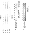
- Fig. 7 is a diagram showing details of the word synchronization detecting circuit 611 and the word synchronization detecting shift register 621.
- the word synchronization detecting circuit 611 comprises inverters 612 to 619 and an AND gate 620.
- the AND gate 620 generates a logical product of the outputs of the serial-parallel converter 604, or the outputs Q 1 , Q 4 , Q 8 , Q 9 , Q 10 , Q 13 and Q 15 , and signals obtained by inverting the outputs Q 0 , Q 2 , Q 3 , Q 5 , Q 6 , Q 7 , Q 12 and Q 14 .
- the output Q 11 of the serial-parallel converter 604 is the previously described busy-idle bit which is unrelated to the word synchronization, it is not connected to the AND gate 620. Therefore, only when the outputs Q 15 to Q 12 and Q 10 to Q 0 of the serial-parallel converter 604 take a value of "101011100010010" equal to the above-mentioned 15-bit word synchronizing character, all the inputs of the AND gate 620 become "1", causing the AND gate 620 to output "1" indicative of detection of the word synchronization character.
- the output of the AND gate 620 is consecutively accepted by the word synchronization detecting shift register 621 which is a 8-bit shift register as shown in Fig.
- the delaying circuit 608 is a 8-bit buffer register comprised of 8 flip-flops as shown in Fig. 8 and simultaneously accepts the 8-bit data Q 0 to Q 7 at a timing of the clock signal RT which has been delayed by a half cycle with respect to the RT ⁇ .
- this 8-bit register 608 is a timing register which has been provided for establishing synchronization with the word synchronization detecting shift register 621.
- the outputs RD 0 to RD 7 of this shift register 608 are applied to a received data output port 609.
- the output port 609 like the above-mentioned output port 622, simultaneously latches the 8-bit input data at a timing of the RT8 ⁇ outputted from the frequency-divider 610.
- Reading-out from the output ports 609 and 622 is performed in response to address signals ARD ⁇ and AWS ⁇ from a 2-bit address line 624 and a read-out signal RD ⁇ , and output of each output port is applied to the control circuit 8 of Fig. 3, through a 8-bit data bus 623.
- Fig. 9 is a block diagram showing details of these output ports 609 and 622.
- the output port 609 includes a 8-bit three-state buffer register 609a which latches the 8-bit outputs RD 0 to RD 7 of the delaying circuit 608 at a timing of the clock RT8 ⁇ from the frequency-dividing circuit 610, and the latched data are, in response to the read-out signal RD ⁇ and the address signal ARD ⁇ , read out on the 8-bit data bus 623 as 8-bit data signals D 0 to D 7 .
- the output port 622 includes a 8-bit three-state buffer register 622a which latches the 8-bit outputs WS 0 to WS 7 from the word synchronization detecting shift register 621 at a timing of the clock RT8 ⁇ , and the latched data are, in response to the read-out signal RD ⁇ and the address signal AWS ⁇ , read out on the 8-bit data bus 623 as 8-bit data signals.
- Fig. 10 is a diagram showing a structure of the three-state buffer register 609a or 622a in Fig. 9, comprising 8 flip-flops connected in parallel, every Q output of which is provided with a gate.
- the buffer registers 609a and 622a are constituted such that their gates open so as to allow the data in the buffer registers to be read out on the data bus 623 only when output enabling is sequentially instructed at different timings for each.
- Fig. 12(a) shows the NRZ data outputted from the received data output port 609, 8 bits by 8 bits in parallel
- Fig. 12(b) shows the word synchronization data outputted from the word synchronization detection output port 622, 8 bits by 8 bits in parallel.
- the synchronization data outputted from the output port 622 has a word synchronization identifying flag "1" in a position corresponding to the word synchronization position in the output signal from the output port 609.
- Fig. 13 is a diagram showing connection relationship between the control circuit 8 and its peripheral units in Fig. 3, where the control circuit 8 is implemented as a microcomputer as shown in Fig. 13.
- the control circuit 8 receives the clock RT8 ⁇ from the data receiver 6, as interruption request from the data receiver 6 and the above-mentioned 8-bit received data or the synchronization data D 0 to D 7 through the data bus 623 as well.
- the control circuit 8 applies, on the other hand, the above-mentioned address signals ARD ⁇ and AWS ⁇ to the data receiver 6 through a 2-bit address line 624.
- the control circuit 8 further applies the read-out signal RD ⁇ for the output ports 609 and 622 above.
- the control circuit 8 supplies the audio processing portion 5, the data transmitter 7 and the LCD driver 12 with required signals for controlling their operation, and monitors operation of the key matrix 11.
- Fig. 14 is a flowchart for explaining operation of the control circuit 8. In the following, operation of the control circuit 8 will be described with reference to Figs. 13 and 14.
- the control circuit 8 resets a flag register F not shown (step S-1) and determines, based on the output signal RT8 ⁇ from the frequency-divider 610 in the data receiver 6, whether there exists any interruption request or not (step S-2).
- processings such as keys scan, LCD drive, audio processing or the like are interrupted so as to accept the 8-bit received data (Fig. 12(a)) and the 8-bit synchronization data (Fig. 12(b)) transmitted from the data receiver 6 through the data bus 623 (step S-3).
- it is determined whether the word synchronization identifying flag "1" as shown in Fig. 12(b) has been contained in the accepted 8-bit synchronization data (step S-4), and if not, the operation returns to step S-2 through step S-9.
- step S-4 if it is determined that the word synchronization identifying flag has been contained in the synchronization data, then the bit position of the flag is detected (step S-5) and those of the received data that follow the bit position are stored in a memory of the control circuit 8 as effective data (step S-6). In this manner, once word synchronization is established, a flag is set in the above-mentioned flag register F (step S-7).
- step S-2 After that, if any interruption request exists (step S-2), irrespective of presence of the word synchronization identifying flag, the received data are stored in the memory (steps S-6 and S-10).
- step S-11 data processings such as busy-idle bit elimination, error correction or the like are executed (step S-12). Meanwhile, the determination of acceptance accomplishment at step S-11 could be made by monitoring the counted value of a word counter which may be provided as being incremented each time data of one word (8 bits) is accepted.
- Fig. 15 is a flowchart showing another example of processing by the control circuit 8.
- step S-21 when interruption request is recognized (step S-21), all of the received data and the synchronization data are first accepted and stored in the memory of the control circuit 8 such that data bits of one data correspond to those of the other, one to one (step S-22), as shown in Fig. 12.
- step S-22 After all of the received data are accepted (step S-23), the position of the word synchronization identifying flag "1" is detected (step S-24) and then data processings are executed according to those received data among the stored data that follow the detected flag position (step S-25).
- step S-25 data processings are executed according to those received data among the stored data that follow the detected flag position
- the word synchronization data which indicates a word synchronizing position, and the received data are processed together as parallel data, a fast recovery of the word synchronization becomes possible, allowing a higher-speed processing of every kind required from a radio communication apparatus.
Description
- The present invention generally relates to synchronization recovery circuits and radiocommunication apparatuses using such circuits, and more particularly, to a synchronization recovery circuit which detects a word synchronizing character in a received data signal for recovering word synchronization in a cellular-type communication system, and to a radiocommunication apparatus such as car telephone and portable telephone using such a synchronization recovery circuit.
- A cellular-type communication system has been widely utilized in the form of a mobile radio telephone such as car telephone or portable telephone. In such a cellular-type communication system, an area to be covered is divided into multiple cells, each of which is provided with a radio base station and assigned a group of channels. Such a small-sized service area of each cell and reduced transmission output of a base station enable frequent reuse of the frequencies, admitting an increased number of subscribers.
- In such a cellular-type communication system, when a mobile station equipped with a radiocommunication apparatus, for example, an automobile equipped with a car telephone moves from one cell to another, several kinds of digital control including channel change or the like are performed in order that complete communications are established between the radio base stations involved and the car telephone apparatus.
- Each radio base station has two types of radio channels, one of which is a bidirectional control channel for such several kinds of digital control as mentioned above, and the other is a bidirectional audio channel for conversation over the telephone.
- For such bidirectional communications, four channel types are employed. More particularly, the control channel comprises a forward control channel (FOCC) used for communication from a radio base station to a mobile station and a reverse control channel (RECC) used for communication from a mobile station to a radio base station, which are generally used for control of every kind before the audio channel is established, and not for conversation. On the other hand, the audio channel comprises a forward audio channel (FVC) used for communication from a radio base station to a mobile station and a reverse audio channel (RVC) used for communication from a mobile station to a radio base station.
- On these channels, a message, or a data signal containing a word synchronizing character is transmitted at predetermined word and bit rates. Therefore, a radiocommunication apparatus of a mobile station is first required to detect the word synchronizing character out of a received data signal for recovering word synchronization. For this purpose, in a conventional radiocommunication apparatus, as disclosed in the US Patent No. 4,029,900, there is provided a synchronization recovery circuit which detects the word synchronizing character out of the data signal for recovering word synchronization. In this synchronization recovery circuit, the word synchronization is recovered by supplying a control circuit for data processing with a word synchronizing signal which has been generated based on the detected word synchronizing character.
- The conventional synchronization recovery circuit, however, is constituted in the light of its hardware construction such that the word synchronizing signal is serially applied to the control circuit. Therefore, in order to recover word synchronization based on such a serial word synchronizing signal, also the data signal must be serially applied to the control circuit. The control circuit receives both of the word synchronizing signal and the data signal serially and accepts the data signal as effective data for use, only after a word synchronizing position is identified. In the above mentioned construction wherein the data signal is adapted to be accepted after word synchronization is established, data may possibly drop out due to high data transmitting rate of the celluar-type communication system. Therefore, the control circuit is always required to access the data signal and thus can not do any other processing such as key scan, LCD display, AF (Analog Frequency) processing, radio-functional processing or the like during the access, prevented from performing any kind of processing required as a mobile station, at a higher speed.
- As one solution to this problem, a control circuit comprised of two microprocessors has been proposed, with one microprocessor performing synchronization recovery of the received data and the other performing any other processing such as key scan. This has led to another problem, however, that the two microprocessors require additional complicated control such as communication control (for example, determination of communication protocol) and timing control between themselves.
- Furthermore, a technology of converting the data signal from serial form to parallel form before supplied to the control circuit has been proposed in Japanese Patent Laying-Open No. 63-245032. Since the word synchronizing signal is supplied in serial form, however, such a parallel data signal in itself does not allow identification of a synchronizing position, so that any software-controlled processing becomes indispensable in the control circuit. More specifically, such software-controlled processing may include a processing for determining a synchronizing character pattern by shifting a data signal bit by bit in order to identifying the position of the synchronizing character in the accepted data signal again. Therefore, with such a technology, a higher operating speed of the radiocommunication apparatus can hardly be attained.
- EP-A-0 052 432 discloses an apparatus for extracting synchronizing information from an incoming serial-bit digital television signal according to the precharacterizing portion of
claim 1 orclaim 13. The incoming serial-bit digital television signal is formed of a sequence of word blocks, each word block being formed of N n-bit words and each word block including a predetermined serial group of n-bits forming said synchronizing information. The apparatus further de-serializes the incoming digital signal in dependency of the synchronizing information. The control means in this apparatus are arranged only to perform synchronization recovery. An additional microprocessor must be provided for performing any other processing. - Additionally there are provided two separate data-buses to read the first and second parallel data into the control means.
- WO 87/01490 discloses a radiotelephone system in which the signalling protocol for the system is embedded in the frame synchronization of the digital messages transmitted on the system. System state communication is achieved by utilizing a sequence of normal synchronization words and the corresponding inverses. Reliability of the coding is achieved by detecting normal or inverse words as binary levels when fewer than a predetermined number of bit errors exist in the bit sequence. If the predetermined number of bit errors is exceeded, a selected binary one or zero is substituted. This selected sequence of binary levels is decoded and the Hamming distance between a masked decoded sequence and a masked selected sequence is calculated. If the Hamming distance calculation yields a number greater than the error correction capability of the coding function, a new set of substituted binary levels is tried, otherwise the decoded sequence is accepted as correct.
- The control means of this system are arranged so as to execute interruption processing in order to recover word synchronization and adapted to execute other processings than the word synchronization recovery except during the time in which said interruption processing is to be executed.
- It is therefore an object of the present invention to provide a synchronization recovery circuit and a radio communication apparatus which has overcome the drawbacks of the state of the art, and which can perform processing at a higher speed in a cellular-typed communication system.
- Another pbject of the present invention is to enable word synchronization recovery of received data with parallel signal processing in a radiocommunication apparatus as a mobile station.
- Briefly stated, according to the present invention, these objects are achieved by the synchronization recovery circuit according to
claim 1 and a radio communication apparatus according toclaim 13. The further claims are related to different advantageous aspects of the present invention. - The main advantage of the present invention is, therefore, that since the received data signal and the word synchronizing signal indicating the synchronizing position thereof are both processed as parallel data, the word synchronization can be quickly recovered and thus all the processings required from a radiocommunication apparatus can be done at a higher speed.
- The foregoing and other objects, features, aspects and advantages of the present invention will become more apparent from the following detailed description of the present invention when taken in conjunction with the accompanying drawings.
- Fig. 1 is a diagram showing a typical format of a forward control channel message.
- Figs. 2 (a) and (b) are diagrams showing specific examples of a bit synchronization field and a word synchronization field, respectively.
- Fig. 3 is a schematic block diagram showing a radiocommunication apparatus according to an embodiment of the present invention.
- Fig. 4 is a block diagram showing an internal structure of the data receiver in the radiocommunication apparatus shown in Fig. 3.
- Fig. 5 is a diagram showing details of the serial-parallel converter shown in Fig. 4.
- Fig. 6 is a block diagram showing details of the 8-bit shift register shown in Fig. 5.
- Fig. 7 is a block diagram showing details of the word synchronization detecting circuit and the word synchronization detecting shift register shown in Fig. 4.
- Fig. 8 is a block diagram showing details of the delaying circuit shown in Fig. 4.
- Fig. 9 is a block diagram showing details of the received data output port and the word synchronization detection output port shown in Fig. 4.
- Fig. 10 is a block diagram showing a structure of the three-state buffer register shown in Fig. 9.
- Fig. 11 is a timing chart for explaining operation of the circuit shown in Fig. 4.
- Fig. 12 is a diagram for schematically explaining operation principles of the circuit shown in Fig. 4.
- Fig. 13 is a block diagram showing details of the control circuit shown in Fig. 3.
- Fig. 14 is a flow chart for explaining operation of the microcomputer shown in Fig. 13.
- Fig. 15 is a flow chart showing another example of processing by the microcomputer shown in Fig. 13.
- In the following, an embodiment of the present invention will be described with reference to the accompanying drawings. The embodiment to be described hereinafter is on a case where the present invention is applied to the forward control channel (FOCC) among the signal paths previously described. On this forward control channel, a forward control channel message (baseband data signal) is transmitted from a radio base station to a mobile station (radiocommunication apparatus), which will perform processings such as registration, channel change or the like according to the received message.
- Fig. 1 is a diagram showing a typical format of such a forward control channel message. This message is largely composited of a bit synchronization field, a word synchronization field and a data message. More particularly, the bit synchronization field is, as shown in Fig. 2 (a), a 10-bit field having alternate 1 and 0 bits recurrent in sequence (known as dotting). The word synchronization field in turn, as shown in Fig. 2 (b), is a 11-bit field having a bit arrangement which is rarely seen in the data message. In the United States, for example, the arrangement of "11100010010" as shown in Fig. 2 (b) is employed. Furthermore, the data message comprises data messages A and B each having 40 bits, which are alternately repeated 5 times for each (designated as A1 to A5 and B1 to B5, respectively). Such 5-time repetition of the respective data messages is for error correction, i.e. for determining effectiveness of data with a coincidence ratio of more than 3/5, or by majority decision when there exists difference between the received data.
- Meanwhile, though not shown in Figs. 1 and 2, one busy-idle bit is added to every 10 bits of the bit synchronization field, the word synchronization field and the respective data messages. This busy-idle bit serves to inform a mobile station of whether the transmission source of the message, or a radio base station is prepared to receive, or of vacancy status of the reverse control channel (RECC). Accordingly, the bit synchronization field, the word synchronization field and the data message are in practice comprised of 11 bits, 12 bits and 44 bits, respectively. The message shown in Fig. 1 will be then transferred, for example in the United States, at a 10 kilobit/second rate after Manchester-encoded in the well-known manner.
- Subsequently, Fig. 3 is a schematic block diagram of a radiocommunication apparatus as a mobile station in a cellular system according to an embodiment of the present invention. In the diagram, an
antenna 3 is connected to areceiver 1 and atransmitter 2 through anantenna coupler 4. Thereceiver 1 FM-demodulates a received signal which has been received from a radio station with theantenna 3. Thereceiver 1 applies a data signal on the forward control channel to adata receiver 6 and a received audio signal on the forward audio channel to anaudio processing circuit 5 by use of a discriminator not shown. Thedata receiver 6 detects a word synchronizing character out of the applied message of FOCC and applies a word synchronizing signal to acontrol circuit 8 constituted of a 8-bit microprocessor, along with the data signal. Thecontrol circuit 8 identifies a synchronizing position of the data signal, based on the applied word synchronizing signal, before executing any kind of control according to the data signal. Thecontrol circuit 8 performs additional processing and control necessary for akey matrix 11 or anLCD driver 12. On the other hand, theaudio processing portion 5 amplifies the applied message of FVC for application to ahandset speaker 10. This enables a user of a mobile station to receive a communication from another. Meanwhile, thecontrol circuit 8 performs control such as muting instruction also for theaudio processing circuit 5. - The
data transmitter 7 Manchester-encodes a data signal from thecontrol circuit 8 for application to thetransmitter 2 as a message for RECC. Meanwhile, theaudio processing circuit 5 processes an audio signal applied from a user through amicrophone 9 for application to thetransmitter 2 as a transmitting audio signal for RVC. Thetransmitter 2 FM-modulates these signals for transmission to a base station by use of theantenna 3. - Meanwhile, a radio base station of each cell is connected to a mobile telephone switching office (MTSO) not shown through a conventional land line or a microwave network. This MTSO is further connected to the public switching telephone network (PSTN), establishing interface between a mobile radio telephone and the PSTN.
- Subsequently, Fig. 4 is a block diagram showing an internal structure of the
data receiver 6 shown in Fig. 3, the respective parts of which are shown in the block diagrams of Figs. 5 to 10 in detail. Furthermore, Fig. 11 is a timing chart showing signals of thedata receiver 6, and Fig. 12 is a diagram for schematically explaining operation principles thereof. - First, a forward control channel message transmitted from a radio base station (not shown) is FM-demodulated in the
receiver 1 and extracted by anLPF 13. The analog forward control channel message extracted by theLPF 13 is digitalized by alimiter 601 before applied to a clocksignal generating circuit 602 and aManchester decoder 603 as a data signal in Manchester code format. The clocksignal generating circuit 602 which is constituted of a well-known PLL (Phase Locked Loop) circuit generates a clock signal RT (Fig. 11(b)) which has been bit-synchronized with the data signal in Manchester code format. This clock signal RT is applied to theManchester decoder 603 and aninverter 607, and also to adelaying circuit 608 and a word synchronization detectingshift register 621 as will be described later. On the other hand, theManchester decoder 603 converts, in response to the data signal and the clock signal RT, the data signal from the Manchester code format to NRZ (Non Return to Zero) format (Fig. 11(a)) and applies the converted signal to a serial-parallel converter 604. This serial-parallel converter 604 has function of a 16-bit shift register and thus converts the serial NRZ data from theManchester decoder 603 into parallel data of 16 bits. - Fig. 5 is a diagram showing a structure of the serial-
parallel converter 604. As shown in the diagram, the serial-parallel converter 604 is comprised of two 8-bit shift registers 
inverter 607 in Fig. 4. Therefore, the shift registers 605 and 606 both operate at a timing of the
shift register 605 consecutively accepts the NRZ data at a timing of
shift register 606. Thisshift register 606 also consecutively accepts the output Q7 of theshift register 605 at a timing of
Manchester decoder 603 is converted into 16-bit parallel data Q0 to Q15, among which the 8-bit data Q0 to Q7 outputted from theshift register 605 are applied to both of thedelaying circuit 608 and the wordsynchronization detecting circuit 611 while the 8-bit data Q8 to Q15 outputted from theshift register 606 are applied to the wordsynchronization detecting circuit 611. Furthermore, Fig. 6 is a diagram showing a structure of the 8-bit shift register - Turning back to Fig. 4, the 16-bit output of the serial-
parallel converter 604 is applied to the wordsynchronization detecting circuit 611. This wordsynchronization detecting circuit 611 detects, based on these data, a word synchronizing character. More particularly, the wordsynchronization detecting circuit 611 detects a 15-bit word synchronizing character composited of the last 4 bits of the bit synchronization field and the 11 bits of the word synchronization field shown in Figs. 1 and 2, i.e. "1010 (bit sync. field) 11100010010 (word sync. field)". Though generally the word synchronizing character may be composited of only the 10 bits of the word synchronization field, the increased bit number of the word synchronizing character which has the last 4 bits of the bit synchronization field added to the original 10 bits of the word synchronization field as described above can reduce the probability that the word synchronizing character may happen to coincide with data of the data message portion, enhancing the precision of word synchronization detection. The output signal of the wordsynchronization detecting circuit 611 is then accepted by the word synchronization detectingshift register 621 at a timing of the clock signal RT. - Fig. 7 is a diagram showing details of the word
synchronization detecting circuit 611 and the word synchronization detectingshift register 621. In the diagram, the wordsynchronization detecting circuit 611 comprisesinverters 612 to 619 and an ANDgate 620. The ANDgate 620 generates a logical product of the outputs of the serial-parallel converter 604, or the outputs Q1, Q4, Q8, Q9, Q10, Q13 and Q15, and signals obtained by inverting the outputs Q0, Q2, Q3, Q5, Q6, Q7, Q12 and Q14. Meanwhile, since the output Q11 of the serial-parallel converter 604 is the previously described busy-idle bit which is unrelated to the word synchronization, it is not connected to the ANDgate 620. Therefore, only when the outputs Q15 to Q12 and Q10 to Q0 of the serial-parallel converter 604 take a value of "101011100010010" equal to the above-mentioned 15-bit word synchronizing character, all the inputs of the ANDgate 620 become "1", causing the ANDgate 620 to output "1" indicative of detection of the word synchronization character. The output of the ANDgate 620 is consecutively accepted by the word synchronization detectingshift register 621 which is a 8-bit shift register as shown in Fig. 7, at a timing of the clock signal RT, or delayed by a half cycle with respect to the
detection output port 622. Theoutput port 622 simultaneously latches the 8-bit input data at a timing of output
divider 610 at which the output
inverter 607 is frequency-divided by 8. - Meanwhile, the outputs Q0 to Q7 of the 8-
bit shift register 605 in the serial-parallel converter 604 are applied to thedelaying circuit 608. Thedelaying circuit 608 is a 8-bit buffer register comprised of 8 flip-flops as shown in Fig. 8 and simultaneously accepts the 8-bit data Q0 to Q7 at a timing of the clock signal RT which has been delayed by a half cycle with respect to the
bit register 608 is a timing register which has been provided for establishing synchronization with the word synchronization detectingshift register 621. The outputs RD0 to RD7 of thisshift register 608 are applied to a receiveddata output port 609. Theoutput port 609, like the above-mentionedoutput port 622, simultaneously latches the 8-bit input data at a timing of the
divider 610. - Reading-out from the
output ports 

bit address line 624 and a read-out signal
control circuit 8 of Fig. 3, through a 8-bit data bus 623. - Fig. 9 is a block diagram showing details of these
output ports output port 609 includes a 8-bit three-state buffer register 609a which latches the 8-bit outputs RD0 to RD7 of thedelaying circuit 608 at a timing of the clock
circuit 610, and the latched data are, in response to the read-out signal

bit data bus 623 as 8-bit data signals D0 to D7. Also theoutput port 622 includes a 8-bit three-state buffer register 622a which latches the 8-bit outputs WS0 to WS7 from the word synchronization detectingshift register 621 at a timing of the clock


bit data bus 623 as 8-bit data signals. - Fig. 10 is a diagram showing a structure of the three-
state buffer register bit data bus 623, the buffer registers 609a and 622a are constituted such that their gates open so as to allow the data in the buffer registers to be read out on thedata bus 623 only when output enabling is sequentially instructed at different timings for each. - Fig. 12(a) shows the NRZ data outputted from the received
data output port detection output port output port 622 has a word synchronization identifying flag "1" in a position corresponding to the word synchronization position in the output signal from theoutput port 609. - Subsequently, Fig. 13 is a diagram showing connection relationship between the
control circuit 8 and its peripheral units in Fig. 3, where thecontrol circuit 8 is implemented as a microcomputer as shown in Fig. 13. Thecontrol circuit 8 receives the clock
data receiver 6, as interruption request from thedata receiver 6 and the above-mentioned 8-bit received data or the synchronization data D0 to D7 through thedata bus 623 as well. Thecontrol circuit 8 applies, on the other hand, the above-mentioned address signals

data receiver 6 through a 2-bit address line 624. Thecontrol circuit 8 further applies the read-out signal
output ports control circuit 8 supplies theaudio processing portion 5, thedata transmitter 7 and theLCD driver 12 with required signals for controlling their operation, and monitors operation of thekey matrix 11. - Furthermore, Fig. 14 is a flowchart for explaining operation of the
control circuit 8. In the following, operation of thecontrol circuit 8 will be described with reference to Figs. 13 and 14. - First, the
control circuit 8 resets a flag register F not shown (step S-1) and determines, based on the output signal
divider 610 in thedata receiver 6, whether there exists any interruption request or not (step S-2). When requested, processings such as keys scan, LCD drive, audio processing or the like are interrupted so as to accept the 8-bit received data (Fig. 12(a)) and the 8-bit synchronization data (Fig. 12(b)) transmitted from thedata receiver 6 through the data bus 623 (step S-3). Subsequently, it is determined whether the word synchronization identifying flag "1" as shown in Fig. 12(b) has been contained in the accepted 8-bit synchronization data (step S-4), and if not, the operation returns to step S-2 through step S-9. - On the other hand, at step S-4, if it is determined that the word synchronization identifying flag has been contained in the synchronization data, then the bit position of the flag is detected (step S-5) and those of the received data that follow the bit position are stored in a memory of the
control circuit 8 as effective data (step S-6). In this manner, once word synchronization is established, a flag is set in the above-mentioned flag register F (step S-7). - After that, if any interruption request exists (step S-2), irrespective of presence of the word synchronization identifying flag, the received data are stored in the memory (steps S-6 and S-10). When acceptance of all the received data is accomplished (step S-11), data processings such as busy-idle bit elimination, error correction or the like are executed (step S-12). Meanwhile, the determination of acceptance accomplishment at step S-11 could be made by monitoring the counted value of a word counter which may be provided as being incremented each time data of one word (8 bits) is accepted.
- Finally, Fig. 15 is a flowchart showing another example of processing by the
control circuit 8. In the example shown in Fig. 15, when interruption request is recognized (step S-21), all of the received data and the synchronization data are first accepted and stored in the memory of thecontrol circuit 8 such that data bits of one data correspond to those of the other, one to one (step S-22), as shown in Fig. 12. After all of the received data are accepted (step S-23), the position of the word synchronization identifying flag "1" is detected (step S-24) and then data processings are executed according to those received data among the stored data that follow the detected flag position (step S-25). The above mentioned detection of the word synchronization identifying flag can be done for every 8 bits, so the high speed processing can be achieved. - While in the embodiment above, description has been made on the case where the present invention is applied to word synchronization recovery for a message on the forward control channel in a receiving system, a circuit of the same structure as described above can be also applied to synchronization recovery of a message on the forward audio channel.
- As has been described in the foregoing, according to the embodiment of the present invention, since the word synchronization data which indicates a word synchronizing position, and the received data are processed together as parallel data, a fast recovery of the word synchronization becomes possible, allowing a higher-speed processing of every kind required from a radio communication apparatus.
- Although the present invention has been described and illustrated in detail, it is clearly understood that the scope of the present invention being limited only by the terms of the appended claims.
Claims (26)
- A synchronization recovery circuit for recovering word synchronization of serial data (NRZ) containing a predetermined word synchronizing character, comprising:data converting means (604, 608) for converting said serial data (NRZ) into first parallel data of n bits, n being an integer equal to or greater than 2, and for latching (609) said first parallel data at a predetermined timing (
 synchronization data generating means (604, 611 and 621) for detecting (604 611) said predetermined word synchronizing character, for generating (621) second parallel data of n bits which indicates a word synchronizing position of said character in said first parallel data, and for latching (622) said second parallel data at said predetermined timing (
 control means (8) for recovering word synchronization of said serial data (NRZ) by identifying said word synchronizing position in said first parallel data based on the second parallel data,characterized in that said control means (8) is arranged for executing interruption processing based on the data whose word synchronisation has been recovered upon receipt of an interruption request (RT8), and for executing any other processing than the word synchronization recovery upon receipt of no interruption request; and in that
said first and second parallel data are read into said
control means through a single data bus (623) at different timings (

- The synchronization recovery circuit according to claim 1, wherein
said data converting mean (604) comprises:first serial-parallel converting means (605) for converting said serial data into said first parallel data at a timing of a predetermined first clock signal ( delaying means (608) for latching said first parallel data outputted from said first serial-parallel converting means at a timing of said second clock signal,first latching means (609) for latching said first parallel data outputted from said delaying means at a timing of a third clock signal (said synchronization data generating means comprises:
 second serial-parallel converting means (605, 606) for converting said serial data into third parallel data of m bits at a timing of said first clock signal, the number m being an integer corresponding to the number of bits of said word synchronizing character;means (611) for determining that said third parallel data coincides with said predetermined word synchronizing character; andthird serial-parallel converting means (621) for converting output of said coincidence determining means into said second parallel data at a timing of a second clock signal (RT) which has been obtained by delaying said first clock signal, andsecond latching means (622) for latching said second parallel data outputted from said third serial-parallel converting means at a timing of said third clock signal,said control means (8) comprises means responsive to said third clock signal for executing interruption processing in which first and second parallel data having been latched in said first and second latching means, respectively, are accepted.
 - The synchronization recovery circuit according to claim 2, wherein
said control means (8) comprises:storage means;means (611) for determining whether a synchronization identifying bit indicative of a word synchronizing position is contained in said accepted second parallel data; andmeans for storing those data among said first parallel data that follow the bit corresponding to said synchronization identifying bit, as effective data into said storage means when it has been determined that said synchronization identifying bit is contained. - The synchronization recovery circuit according to claim 2, wherein
said control means (8) comprises:storage means;means for storing said accepted first and second parallel data into said storage means such that data bits of one data correspond to those of the other, one to one;means for determining whether the synchronization identifying bit indicative of a word synchronizing position is contained in said second parallel data stored in said storage means; andmeans for using those data among said first parallel data that follow the bit corresponding to said synchronization identifying bit, as effective data for data processing when it has been determined that said synchronization identifying bit is contained. - The synchronization recovery circuit according to claim 2, wherein
said first serial-parallel converting means (605) comprises an n-bit shift register. - The synchronization recovery circuit according to claim 2, wherein
said second serial-parallel converting means (605, 606) comprises an m-bit shift register. - The synchronization recovery circuit according to claim 2, wherein
said coincidence determining means (611) comprises logic circuit means having m inputs. - The synchronization recovery circuit according to claim 2, wherein
said third serial-parallel converting means (621) comprises an n-bit shift register. - The synchronization recovery circuit according to claim 2, wherein
said delaying means (608) comprises an n-bit buffer register. - The synchronization recovery circuit according to claim 2, wherein
each of said first and second latching means (609, 622) comprises an n-bit three-state buffer register whose reading operation is controlled by said control means. - The synchronization recovery circuit according to claim 1, wherein
said serial data is a forward control channel message in a cellular-type communication system. - The synchronization recover circuit according to claim 1, wherein
said serial data is a forward audio channel message in a cellular-type communication system. - A radiocommunication apparatus which at least has a function of receiving data outputted from a radio base station, comprising:means (3, 4, 1) for receiving and demodulating said transmitted data;means (13, 601, 602 and 603) for extracting serial data containing a predetermined word synchronizing character out of said received data; andsynchronization recovering means for recovering word synchronization of said serial data, whereinsaid synchronization recovering means comprises:data converting means (604) for converting said serial data into first parallel data of n bits, n being an integer equal to or greater than 2, and for latching (609) said first parallel data at a predetermined timing (
 synchronization data generating means (604, 611 and 621) for detecting (604, 611) said predetermined word synchronizing character, for generating (621) second parallel data of n bits which indicates a word synchronizing position of said character in said first parallel data, and for latching (622) said second parallel data at said predetermined timing (
 control means (8) for recovering word synchronization of said serial data by identifying said word synchronizing position in said first parallel data based on said second parallel datacharacterized in thatsaid control means (8) is arranged, upon receipt of an interruption request (RT8), to perform the required processings based on the data whose word synchronization has been recovered, and for executing any other processing than the word synchronization recovery upon receipt of no interruption request; and in thatsaid first and second parallel data are read into said control means through a single data bus (623) at different timings (

- The radiocommunication apparatus according to claim 13, wherein
said data converting means (604) comprises:first serial-parallel converting means (605) for converting said serial data into said first parallel data at a timing of a predetermined first clock signal ( delaying means (608) for latching said first parallel data outputted from said first serial-parallel converting means at a timing of said second clock signal,first latching means (609) for latching said first parallel data outputted from said delaying means at a timing of a third clock signal (said synchronization data generating means comprises:
 second serial-parallel converting means (605, 606) for converting said serial data into third parallel data of m bits at a timing of a said first clock signal, the number m being an integer corresponding to the number of bits of said word synchronizing character;means (611) for determining that said third parallel data coincides with said predetermined word synchronizing character; andthird serial-parallel converting means (621) for converting output of said coincidence determining means into said second parallel data at a timing of a second clock signal (RT) which has been obtained by delaying said first clock signal,second latching means (622) for latching said second parallel data outputted from said serial-parallel converting means at a timing of said third clock signal; andsaid control means (8) comprises means responsive to said third clock signal for executing interruption processing in which first and second parallel data having been latched in said first and second latching means, respectively, are accepted.
 - The radiocommunication apparatus according to claim 14, wherein
said control means comprises:storage means;means for determining whether a synchronization identifying bit indicative of a word synchronizing position is contained in said accepted second parallel data; andmeans for storing those data among said first parallel data that follow the bit corresponding to said synchronization identifying bit, as effective data into said storage means when it has been determined that said synchronization identifying bit is contained. - The radiocommunication apparatus according to claim 14, wherein
said control means comprises:storage means;means for storing said accepted first and second parallel data into said storage means such that data bits of one data correspond to those of the other, one to one;means for determining whether a synchronization identifying bit indicative of a word synchronizing position is contained in said second parallel data stored in said storage means; andmeans for using those data among said first parallel data that follow the bit corresponding to said synchronization identifying bit, as effective data for data processing when it has been determined that said synchronization identifying bit is contained. - The radiocommunication apparatus according to claim 14, wherein
said first serial-parallel converting means (605) comprises an n-bit shift register. - The radiocommunication apparatus according to claim 14, wherein
said second serial-parallel converting means (605, 606) comprises an m-bit shift register. - The radiocommunication apparatus according to claim 14, wherein
said coincidence determining means (611) comprises logic circuit means having m inputs. - The radiocommunication apparatus according to claim 14, wherein
said third serial-parallel converting means (621) comprises an n-bit shift register. - The radiocommunication apparatus according to claim 14, wherein
said delaying means (608) comprises an n-bit buffer register. - The radiocommunication apparatus according to claim 14, wherein
each of said first and second latching means (609, 622) comprises an n-bit three-state buffer register whose reading operation is controlled by said control means. - The radiocommunication apparatus according to claim 13, wherein
said serial data is a forward control channel message in a cellular-type communication system. - The radiocommunication apparatus according to claim 13, wherein
said serial data is a forward audio channel message in a cellular-type communcation system. - The radiocommunication apparatus according to claim 13, further comprising:
audio processing means (5) for extracting data comprising an audio signal out of said received data and processing the same. - The radiocommunication apparatus according to claim 25, further comprising:
means (2 and 7) for receiving data from said control means and said audio processing means, and transmitting the same to said radio base station.
Applications Claiming Priority (2)
| Application Number | Priority Date | Filing Date | Title |
|---|---|---|---|
| JP32109688 | 1988-12-20 | ||
| JP321096/88 | 1988-12-20 |
Publications (3)
| Publication Number | Publication Date |
|---|---|
| EP0374906A2 EP0374906A2 (en) | 1990-06-27 |
| EP0374906A3 EP0374906A3 (en) | 1991-06-26 |
| EP0374906B1 true EP0374906B1 (en) | 1997-03-05 |
Family
ID=18128774
Family Applications (1)
| Application Number | Title | Priority Date | Filing Date |
|---|---|---|---|
| EP89123599A Expired - Lifetime EP0374906B1 (en) | 1988-12-20 | 1989-12-20 | Synchronization recovery circuit for recovering word synchronization and radiocommunication apparatus using the same |
Country Status (5)
| Country | Link |
|---|---|
| US (1) | US5040195A (en) |
| EP (1) | EP0374906B1 (en) |
| KR (1) | KR0160279B1 (en) |
| CA (1) | CA2006250C (en) |
| DE (1) | DE68927823T2 (en) |
Families Citing this family (22)
| Publication number | Priority date | Publication date | Assignee | Title |
|---|---|---|---|---|
| US5258980A (en) * | 1989-08-25 | 1993-11-02 | Nippon Telegraph And Telephone Corporation | Radio channel switching control method |
| FR2664765B1 (en) * | 1990-07-11 | 2003-05-16 | Bull Sa | DEVICE FOR SERIALIZATION AND DESERIALIZATION OF DATA AND SYSTEM FOR DIGITAL TRANSMISSION OF SERIAL DATA THEREOF. |
| JP2666679B2 (en) * | 1993-04-27 | 1997-10-22 | 日本電気株式会社 | Slot reception synchronization circuit |
| KR970002845B1 (en) * | 1993-12-31 | 1997-03-12 | 엘지전자 주식회사 | Demodulation apparatus for digital audio signal |
| JP2975857B2 (en) * | 1994-11-21 | 1999-11-10 | 三洋電機株式会社 | Wireless communication device |
| US5764648A (en) * | 1994-07-20 | 1998-06-09 | Sanyo Electric Co., Ltd. | Method and apparatus for generating a transmission timing signal in a wireless telephone |
| US5787114A (en) * | 1996-01-17 | 1998-07-28 | Lsi Logic Corporation | Loop-back test system and method |
| US5956370A (en) * | 1996-01-17 | 1999-09-21 | Lsi Logic Corporation | Wrap-back test system and method |
| US5781544A (en) * | 1996-01-17 | 1998-07-14 | Lsi Logic Corporation | Method for interleaving network traffic over serial lines |
| US5896426A (en) * | 1996-02-05 | 1999-04-20 | Lsi Logic Corporation | Programmable synchronization character |
| US5781038A (en) * | 1996-02-05 | 1998-07-14 | Lsi Logic Corporation | High speed phase locked loop test method and means |
| US5790563A (en) * | 1996-02-05 | 1998-08-04 | Lsi Logic Corp. | Self test of core with unpredictable latency |
| JP3441589B2 (en) * | 1996-02-29 | 2003-09-02 | シャープ株式会社 | Synchronous detection and demodulation circuit |
| US6574756B1 (en) * | 1998-08-31 | 2003-06-03 | International Business Machines Corporation | Method and apparatus for identifying the start of a data field using a fault tolerant sync word |
| DE19961131A1 (en) * | 1999-12-17 | 2002-07-18 | Siemens Ag | Device and method for compensating data transit times |
| US6977969B2 (en) * | 2000-06-28 | 2005-12-20 | Samsung Electronics Co., Ltd. | Digital FM receiver for recovering FM digital data frame in mobile communication system |
| WO2002030036A1 (en) * | 2000-10-06 | 2002-04-11 | Flextronics Semiconductor Design, Inc. | Coherent expandable high speed interface |
| US7352777B2 (en) * | 2001-10-31 | 2008-04-01 | Intel Corporation | Data framer |
| US7188290B2 (en) * | 2002-04-23 | 2007-03-06 | Intel Corporation | Data alignment for telecommunications networks |
| JP3704709B2 (en) * | 2002-10-02 | 2005-10-12 | 日本電気株式会社 | Data resynchronizer |
| US7613263B2 (en) * | 2003-03-04 | 2009-11-03 | Altera Corporation | Clock and data recovery method and apparatus |
| JP4796983B2 (en) * | 2007-03-08 | 2011-10-19 | オンセミコンダクター・トレーディング・リミテッド | Serial / parallel conversion circuit, liquid crystal display drive circuit |
Family Cites Families (17)
| Publication number | Priority date | Publication date | Assignee | Title |
|---|---|---|---|---|
| US3308434A (en) * | 1963-01-09 | 1967-03-07 | Teletype Corp | Synchronization circuit for signal generators using comparison of a specific data message |
| US3760355A (en) * | 1972-03-08 | 1973-09-18 | Motorola Inc | Digital pattern detector |
| US3909724A (en) * | 1973-06-26 | 1975-09-30 | Addressograph Multigraph | Start bit detector and data strober for asynchronous receiver |
| US4029900A (en) * | 1976-01-26 | 1977-06-14 | Bell Telephone Laboratories, Incorporated | Digital synchronizing signal recovery circuits for a data receiver |
| US4107459A (en) * | 1977-05-16 | 1978-08-15 | Conic Corporation | Data processor analyzer and display system |
| GB2089178B (en) * | 1980-11-18 | 1984-07-04 | Sony Corp | Digital signal processing |
| CH656760A5 (en) * | 1981-11-11 | 1986-07-15 | Landis & Gyr Ag | METHOD AND ARRANGEMENT FOR ENSURING THE START SYNCHRONIZATION OF A TELEGRAM CONSTRUCTED FROM BIT-PULSE SEQUENCES WITHIN A RECEIVER. |
| JPS5890837A (en) * | 1981-11-19 | 1983-05-30 | Nec Corp | Signal detecting circuit |
| US4450572A (en) * | 1982-05-07 | 1984-05-22 | Digital Equipment Corporation | Interface for serial data communications link |
| JPS58200654A (en) * | 1982-05-18 | 1983-11-22 | Nec Corp | Communication device |
| US4726014A (en) * | 1983-01-11 | 1988-02-16 | U.S. Holding Company, Inc. | Cellular mobile radio service telephone system |
| JPS6068787A (en) * | 1983-09-26 | 1985-04-19 | Hitachi Ltd | Framing code detecting circuit |
| GB2174567A (en) * | 1985-04-29 | 1986-11-05 | Philips Electronic Associated | Deriving frame interval signals |
| EP0235179A1 (en) * | 1985-08-30 | 1987-09-09 | Motorola, Inc. | Radiotelephone system employing digitized speech/data and embedded signalling |
| JPH0775343B2 (en) * | 1986-02-14 | 1995-08-09 | 株式会社日立製作所 | Synchronization detection circuit and method |
| GB8609499D0 (en) * | 1986-04-18 | 1986-05-21 | Gen Electric Co Plc | Digital transmission system |
| JPS63245032A (en) * | 1987-03-31 | 1988-10-12 | Fujitsu Ltd | High speed frame synchronizing system |
-
1989
- 1989-12-19 KR KR1019890018894A patent/KR0160279B1/en not_active IP Right Cessation
- 1989-12-19 US US07/452,668 patent/US5040195A/en not_active Expired - Lifetime
- 1989-12-20 DE DE68927823T patent/DE68927823T2/en not_active Expired - Lifetime
- 1989-12-20 CA CA002006250A patent/CA2006250C/en not_active Expired - Lifetime
- 1989-12-20 EP EP89123599A patent/EP0374906B1/en not_active Expired - Lifetime
Also Published As
| Publication number | Publication date |
|---|---|
| DE68927823D1 (en) | 1997-04-10 |
| CA2006250C (en) | 2000-06-13 |
| KR900011208A (en) | 1990-07-11 |
| EP0374906A2 (en) | 1990-06-27 |
| US5040195A (en) | 1991-08-13 |
| EP0374906A3 (en) | 1991-06-26 |
| DE68927823T2 (en) | 1997-09-18 |
| KR0160279B1 (en) | 1998-12-01 |
| CA2006250A1 (en) | 1990-06-20 |
Similar Documents
| Publication | Publication Date | Title |
|---|---|---|
| EP0374906B1 (en) | Synchronization recovery circuit for recovering word synchronization and radiocommunication apparatus using the same | |
| US5715278A (en) | Standby power saving in mobile phones | |
| US4302845A (en) | Phase-encoded data signal demodulator | |
| AU736246B2 (en) | A method and an arrangement for controlling scanning of radio channels by a mobile station operating in standby mode | |
| US5099477A (en) | Phase matching circuit | |
| JP2002537671A (en) | Slotted idle mode for dual mode subscriber stations | |
| JPH06315025A (en) | Slot reception synchronizing circuit | |
| US5898736A (en) | Data receiving system | |
| JP2609934B2 (en) | Sync recovery circuit to recover word sync | |
| JP2730463B2 (en) | Radio selective call receiver | |
| US5265105A (en) | Decoding circuit for inhibiting error propagation | |
| US5799050A (en) | Sync detection circuit and method using variable reference for comparison with mismatch count | |
| JPH098671A (en) | Bus transmission system | |
| EP0579039B1 (en) | Synchronous detecting apparatus and synchronous detecting and protecting method | |
| EP1396955B1 (en) | Bit error rate measuring circuit in cases synchronization cannot be established | |
| JP3180960B2 (en) | Message extraction method for cellular telephone receiver | |
| JP4338850B2 (en) | Frame synchronization method and mobile station apparatus and relay station apparatus using the frame synchronization method | |
| JP2000174744A (en) | Frame synchronization circuit | |
| JP3182312B2 (en) | Wireless communication device | |
| JPH09307531A (en) | Method and device for bit error rate measurement | |
| JP3290331B2 (en) | Block synchronization processing circuit | |
| JP3223576B2 (en) | Data receiving device | |
| JP3059914B2 (en) | Wireless communication device | |
| JP3426856B2 (en) | Communication device | |
| JPS61137447A (en) | Decoding device for multiphase psk signal |
Legal Events
| Date | Code | Title | Description |
|---|---|---|---|
| PUAI | Public reference made under article 153(3) epc to a published international application that has entered the european phase |
Free format text: ORIGINAL CODE: 0009012 |
|
| AK | Designated contracting states |
Kind code of ref document: A2 Designated state(s): DE FR GB IT SE |
|
| 17P | Request for examination filed |
Effective date: 19901228 |
|
| PUAL | Search report despatched |
Free format text: ORIGINAL CODE: 0009013 |
|
| AK | Designated contracting states |
Kind code of ref document: A3 Designated state(s): DE FR GB IT SE |
|
| 17Q | First examination report despatched |
Effective date: 19940126 |
|
| GRAG | Despatch of communication of intention to grant |
Free format text: ORIGINAL CODE: EPIDOS AGRA |
|
| GRAH | Despatch of communication of intention to grant a patent |
Free format text: ORIGINAL CODE: EPIDOS IGRA |
|
| GRAH | Despatch of communication of intention to grant a patent |
Free format text: ORIGINAL CODE: EPIDOS IGRA |
|
| GRAA | (expected) grant |
Free format text: ORIGINAL CODE: 0009210 |
|
| AK | Designated contracting states |
Kind code of ref document: B1 Designated state(s): DE FR GB IT SE |
|
| PG25 | Lapsed in a contracting state [announced via postgrant information from national office to epo] |
Ref country code: IT Free format text: LAPSE BECAUSE OF FAILURE TO SUBMIT A TRANSLATION OF THE DESCRIPTION OR TO PAY THE FEE WITHIN THE PRESCRIBED TIME-LIMIT;WARNING: LAPSES OF ITALIAN PATENTS WITH EFFECTIVE DATE BEFORE 2007 MAY HAVE OCCURRED AT ANY TIME BEFORE 2007. THE CORRECT EFFECTIVE DATE MAY BE DIFFERENT FROM THE ONE RECORDED. Effective date: 19970305 |
|
| REF | Corresponds to: |
Ref document number: 68927823 Country of ref document: DE Date of ref document: 19970410 |
|
| ET | Fr: translation filed | ||
| PLBE | No opposition filed within time limit |
Free format text: ORIGINAL CODE: 0009261 |
|
| STAA | Information on the status of an ep patent application or granted ep patent |
Free format text: STATUS: NO OPPOSITION FILED WITHIN TIME LIMIT |
|
| 26N | No opposition filed | ||
| REG | Reference to a national code |
Ref country code: GB Ref legal event code: IF02 |
|
| PGFP | Annual fee paid to national office [announced via postgrant information from national office to epo] |
Ref country code: SE Payment date: 20081205 Year of fee payment: 20 |
|
| PGFP | Annual fee paid to national office [announced via postgrant information from national office to epo] |
Ref country code: FR Payment date: 20081212 Year of fee payment: 20 |
|
| PGFP | Annual fee paid to national office [announced via postgrant information from national office to epo] |
Ref country code: DE Payment date: 20081219 Year of fee payment: 20 |
|
| PGFP | Annual fee paid to national office [announced via postgrant information from national office to epo] |
Ref country code: GB Payment date: 20081217 Year of fee payment: 20 |
|
| REG | Reference to a national code |
Ref country code: GB Ref legal event code: PE20 Expiry date: 20091219 |
|
| PG25 | Lapsed in a contracting state [announced via postgrant information from national office to epo] |
Ref country code: GB Free format text: LAPSE BECAUSE OF EXPIRATION OF PROTECTION Effective date: 20091219 |