EP0374845A2 - Method and apparatus for driving a liquid crystal display panel - Google Patents
Method and apparatus for driving a liquid crystal display panel Download PDFInfo
- Publication number
- EP0374845A2 EP0374845A2 EP89123476A EP89123476A EP0374845A2 EP 0374845 A2 EP0374845 A2 EP 0374845A2 EP 89123476 A EP89123476 A EP 89123476A EP 89123476 A EP89123476 A EP 89123476A EP 0374845 A2 EP0374845 A2 EP 0374845A2
- Authority
- EP
- European Patent Office
- Prior art keywords
- voltage
- data
- electrodes
- scan
- liquid crystal
- Prior art date
- Legal status (The legal status is an assumption and is not a legal conclusion. Google has not performed a legal analysis and makes no representation as to the accuracy of the status listed.)
- Granted
Links
Images


Classifications
-
- G—PHYSICS
- G09—EDUCATION; CRYPTOGRAPHY; DISPLAY; ADVERTISING; SEALS
- G09G—ARRANGEMENTS OR CIRCUITS FOR CONTROL OF INDICATING DEVICES USING STATIC MEANS TO PRESENT VARIABLE INFORMATION
- G09G3/00—Control arrangements or circuits, of interest only in connection with visual indicators other than cathode-ray tubes
- G09G3/20—Control arrangements or circuits, of interest only in connection with visual indicators other than cathode-ray tubes for presentation of an assembly of a number of characters, e.g. a page, by composing the assembly by combination of individual elements arranged in a matrix no fixed position being assigned to or needed to be assigned to the individual characters or partial characters
- G09G3/34—Control arrangements or circuits, of interest only in connection with visual indicators other than cathode-ray tubes for presentation of an assembly of a number of characters, e.g. a page, by composing the assembly by combination of individual elements arranged in a matrix no fixed position being assigned to or needed to be assigned to the individual characters or partial characters by control of light from an independent source
- G09G3/36—Control arrangements or circuits, of interest only in connection with visual indicators other than cathode-ray tubes for presentation of an assembly of a number of characters, e.g. a page, by composing the assembly by combination of individual elements arranged in a matrix no fixed position being assigned to or needed to be assigned to the individual characters or partial characters by control of light from an independent source using liquid crystals
- G09G3/3611—Control of matrices with row and column drivers
- G09G3/3696—Generation of voltages supplied to electrode drivers
-
- G—PHYSICS
- G09—EDUCATION; CRYPTOGRAPHY; DISPLAY; ADVERTISING; SEALS
- G09G—ARRANGEMENTS OR CIRCUITS FOR CONTROL OF INDICATING DEVICES USING STATIC MEANS TO PRESENT VARIABLE INFORMATION
- G09G3/00—Control arrangements or circuits, of interest only in connection with visual indicators other than cathode-ray tubes
- G09G3/20—Control arrangements or circuits, of interest only in connection with visual indicators other than cathode-ray tubes for presentation of an assembly of a number of characters, e.g. a page, by composing the assembly by combination of individual elements arranged in a matrix no fixed position being assigned to or needed to be assigned to the individual characters or partial characters
- G09G3/34—Control arrangements or circuits, of interest only in connection with visual indicators other than cathode-ray tubes for presentation of an assembly of a number of characters, e.g. a page, by composing the assembly by combination of individual elements arranged in a matrix no fixed position being assigned to or needed to be assigned to the individual characters or partial characters by control of light from an independent source
- G09G3/36—Control arrangements or circuits, of interest only in connection with visual indicators other than cathode-ray tubes for presentation of an assembly of a number of characters, e.g. a page, by composing the assembly by combination of individual elements arranged in a matrix no fixed position being assigned to or needed to be assigned to the individual characters or partial characters by control of light from an independent source using liquid crystals
- G09G3/3611—Control of matrices with row and column drivers
- G09G3/3622—Control of matrices with row and column drivers using a passive matrix
-
- G—PHYSICS
- G09—EDUCATION; CRYPTOGRAPHY; DISPLAY; ADVERTISING; SEALS
- G09G—ARRANGEMENTS OR CIRCUITS FOR CONTROL OF INDICATING DEVICES USING STATIC MEANS TO PRESENT VARIABLE INFORMATION
- G09G2320/00—Control of display operating conditions
- G09G2320/02—Improving the quality of display appearance
- G09G2320/0209—Crosstalk reduction, i.e. to reduce direct or indirect influences of signals directed to a certain pixel of the displayed image on other pixels of said image, inclusive of influences affecting pixels in different frames or fields or sub-images which constitute a same image, e.g. left and right images of a stereoscopic display
Abstract
Description
- The present invention relates to methods and circuit configuration for driving a liquid crystal display panels of direct drive type.
- In driving methods of liquid crystal display devices, there are two major categories, i.e. a direct drive matrix type and an active matrix type. The active matrix type experiences difficulties in its production because active elements are required on every picture element at intersections of the matrix. Therefore, the direct drive matrix type has been widely employed for display panels having a large number of the picture elements.
- It is widely known that in the liquid crystal display panel of the direct drive matrix, when data pulse voltages are applied onto selected data electrodes an undesirable spike voltage is induced on the unselected scan electrodes facing the data electrodes, through electrostatic capacitances of liquid crystal cells (referred to hereinafter as cells) connected to the data electrodes. The spike voltage is caused by differentiation of the change in the applied data pulse voltages by the cell capacitances. Optical transparency of each cell corresponds to an effective value, i.e. a square root of sum of squares of applied cell voltages for the voltage application period. Thus induced spike voltages on the unselected scan electrodes cause a cross-talk, i.e. non-uniformity, to develop on the display panel. Recent trend of increase in electrodes quantity on a larger panel causes not only an increase in electrical resistance of transparent electrodes but also a decrease in difference of the applied cell voltage to select on ON-STATE of the cell, where the cell is most transparent by an application of cell voltages, from a voltage to select an OFF-STATE, where the cell is least transparent by the least application of the cell voltages. Therefore, the cross-talk has been becoming more and more serious problem.
- In order to eliminate the effect of such indesirably induced spike voltages, some methods have been proposed as described below. In Japanese un-examined patent publication Sho 63-240528, there is disclosed an idea that a compensation voltage is applied to unselected electrodes. However , none of its practical means is disclosed therein. In Japanese un-examined patent publication Sho 63-220228, there is disclosed a method that a voltage corresponding to the display data on a selected scan electrode is fed back to unselected scan electrodes. However, in these methods, it is impossible to compensate a cross-talk on the display which is caused from a change in the quantity of ON-STATE cells when the scan goes to a presently selected scan electrode from the just previously selected scan electrode.
- It is a general object of the invention, therefore to provide methods and circuit configuration to cancel a cross-talk which develops on cells on unselected scan electrodes, caused from a change in the quantity of ON-STATE cells when the scan moves to a presently selected scan electrode from the just previously selected scan electrode.
- In a method of the present invention, a quantity of ON-STATE cells (or OFF-STATE cells) displayed on the just previous scan electrode is counted and a quantity of ON-STATE cells (or OFF-STATE cells) to be displayed on a present scan electrode is counted. A compensation voltage is generated according to a predetermined relation based on a difference of the two above-counted quantities, and is superposed onto drive voltages of unselected scan electrodes or of each of data electrodes, in a polarity that an effect of undesirable spike voltages induced on the unselected cell voltages are cancelled, in synchronization with selection of the present scan electrode.
- The above-described relation of the compensation voltage versus the counted quantity difference may be proportional or may be given with a predetermined specific relation to meet the panel characteristics. The compensation voltage may be a DC voltage during the period for selecting the single scan electrode or may be of a spike waveform. Amplitude of this spike is determined by the above-described predetermined relation.
- The above-mentioned features and advantages of the present invention, together with other objects and advantages, which will become apparent, will be more fully described hereinafter, with reference being made to the accompanying drawings which form a part hereof, wherein like numerals refer to like parts throughout.
-
- FIG. 1 is a block diagram of a first preferred embodiment of the present invention;
- FIGs. 2 show voltages to be applied upon scan and data electrodes according to an optimized amplitude selection method;
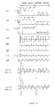
- FIGs. 3 show voltage waveforms in the circuit of the FIG. 1 first preferred embodiment;
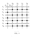
- FIG. 4 is a pattern displayed by the waveforms shown in FIGs. 3;
- FIG. 5 is a block diagram of a second preferred embodiment of the present invention;
- FIG. 6 is a block diagram of a third preferred embodiment of the present invention;
- FIGs. 7 show voltage waveforms in the circuit of the FIG. 6 third preferred embodiment;
- FIG. 8 is a block diagram of a fourth preferred embodiment of the present invention;
- FIGs. 9 show voltage waveforms in the circuit of the FIG. 8 fourth preferred embodiment;
- FIG. 10 is a block diagram of a fifth preferred embodiment of the present invention;
- FIG. 11 is a block diagram of a sixth preferred embodiment of the present invention;
- FIG. 12 is a block diagram of a seventh preferred embodiment of the present invention;
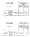
- FIG. 13 is a table exhibiting an amount of adjusted compensation, employed in the seventh preferred embodiment;
- FIG. 14 is a block diagram of a eighth preferred embodiment of the present invention;
- FIGs. 15 show voltage waveforms in the circuit of the FIG. 14 eighth preferred embodiment;
- FIG. 16 is a block diagram of a ninth preferred embodiment of the present invention;
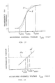
- FIG. 17 shows relation of cell brightness versus brightness control voltage; and
- FIG. 18 shows relation of adjusted compensation voltage versus brightness control voltage, embodied in the ninth preferred embodiment.
- Referring to drawings, preferred embodiments of the present invention are hereinafter described in detail.
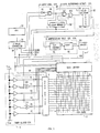
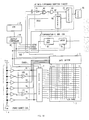
- FIG. 1 shows a first preferred embodiment of the present invention. Data electrodes X₁ ∼ Xn and scan electrodes Y₁ ∼ Ym form a matrix configuration for a liquid crystal display panel (referred to hereinafter as panel) 3, and are connected to a
data driver 1 andscan driver 2, respectively. A cell located at an intersection of a scan electrode and data electrode becomes ON-STATE by application of the below-described selective cell voltages onto the crossing two electrodes, and becomes OFF-STATE by application of the below-described unselective cell voltages thereto. Thus, the cell is distinguished to optically display the data given thereto.Data driver 1 is supplied with DC (direct current) voltages, V volts [V₁], (1-2/a)V volts [V₃], (2/a)V volts [V₄] and 0 volt [V₆], frompower source circuit 4.Scan driver 2 is supplied with DC voltages, outputting V volts [V₁] and 0 volt [V₆] directly frompower source circuit 4 and DC voltages (1-1/a)V volts (V₂] and (1/a)V volts [V₅] frompower source circuit 4 via first input terminals ofadder circuits - A
display controller 15, outputs todata driver 1 an X data (a display signal) XD to be displayed on theliquid crystal panel 3 and to scan driver 2 a Y data (a scan signal) YD to sequentially select one of the scan electrodes, in response to an instruction given from amain controller 19, such as a CPU (central processing unit).Data driver 1 andscan driver 2 selectively output one of the above-described selective and unselective voltages received from thepower source circuit 4 to each of the data electrodes X₁ ∼ Xn and scan electrodes Y₁ ∼ Ym, respectively, in response to the X data and Y data. Selection of these voltages will be described later on. The X data to be displayed on the scan electrodes is serially input from thedisplay controller 15, and is once latched in a shift-register (not shown in the figure) provided in thedata driver 1 and is output in a parallel form in synchronization with the selection of a scan electrode Yi on which the X data XDi is to be displayed. - In the present invention, a well-known Optimized Amplitude Selection Method which was reported by Allen R. Kmetz on Seminar Lecture Note, page 7.2-2 to 7.2-24, for the Society of Information Display, 1984, is employed so that the liquid crystal cells are prevented from deterioration of display characteristics by eliminating a residual DC voltage on the cells. That is, a positive voltage application mode where the selective cell voltage defined with respect to the scan electrode potential is positive, and a negative voltage application mode where the cell voltage is negative with respect to the scan electrode potential, are alternately switched in a predetermined cycle. This switching cycle is, for example, each frame (a screen) or several scan electrodes. In the preferred embodiments of the present invention, the frame cycle is selected as the switching cycle. Application voltages onto the scan and data electrodes in the positive and voltage application modes are respectively shown in FIG. 2(a) and FIG. 2(b), where the voltages enclosed by dotted lines indicate cell voltages with respect to the scan electrode. A constant "a" included in the formulas representing the application voltages is given by a formula, a = √N + 1, where N indicates the quantity of the scan electrodes. Therefore, in the present preferred embodiment where the quantity of the scan electrodes is 400, a = 21, the selective voltage V in FIGs. 2 is 36.2 volts depending on the quantity of the scan electrodes and on the liquid crystal material used in the panel. Accordingly, the voltages V₂, V₃, V₄, and V₅ each defined by the formulas including the constant "a" are 0.95V volts, 0.90V volts, 0.10V volts and 0.05V volts, respectively. V₆ is 0 volt. The voltages V₁ to V₆ are provided from a positive power source voltage Vcc and a negative power source voltage Vee, through divider resistors.
- In driving the
panel 3 in the positive voltage application mode thedata driver 1 applies the voltage V onto data electrode(s) to be selected (i.e. to become ON-STATE) and the voltage (1-2/a)V volts to data electrode(s) to be unselected (i.e. to become OFF-STATE) depending on the received X data XD, while thescan driver 2 applies 0 volt onto a scan electrode to be selected as well as (1-1/a)V volts onto all other unselected scan electrodes. In driving thepanel 3 in the negative voltage application mode thedata driver 1 applies 0 volt onto selected data electrode(s) and the voltage (2/a)V volts to unselected data electrode(s), while thescan driver 2 applies V volts onto a selected scan electrode as (1/a)V volts onto all other unselected scan electrodes. -
Display controller 15 has an output terminal 151 to output a frame signal (i.e. a mode selecting signal) DF which selects the voltage application mode in the predetermined cycle, each time a transmission of the single frame data is completed. The mode selecting signal DF is input todata driver 1, scandriver 2, and aninverter 61 comprised in a below-describedlogic converter 6, respectively.Data driver 1 and scandriver 2 are set in the positive voltage application mode by, for example,logic level 1 of the mode selecting signal DF and the negative voltage application mode by thelogic level 0. - When a scan electrode Yi is going to be selected, X data XDi to be displayed on this scan electrode Yi are serially output from the
display controller 15, then, the X data XDi is input to both thedata driver 1 and thelogic converting circuit 6. In the figures, suffix "i" and "i-l" indicating the scan electrode number are omitted from XD, XD′, XD˝ denoting the X data.Data driver 1 latches the X data XDi, and outputs the latched data Xi when the scan electrode Yi is selected by an application of selective scan voltages, as described above.Logic converting circuit 6 converts an ON-STATE signal and OFF-STATE signal each in the X data XDi according to the below-described routine.Logic converting circuit 6 comprises aninverter 61 and an exclusive ORgate 62.Inverter 61 is input with the mode selecting signal DF as described above, and the exclusive ORgate 62 is input with the output of theinverter 61 and the X data XDi. Because the mode selecting signal DF is inverted by theinverter 61, logic level "1" in the X data XDi for scan electrode Yi is output as it is from thelogic converting circuit 6 to the exclusive ORgate 811, without being converted during the positive voltage application mode; in other words, an ON-STATE signal is output as logic "1" level from thelogic converting circuit 6 and an OFF-STATE signal as logic level "0". On the contrary, during the negative voltage application mode, an ON-STATE signal, i.e. logic level "1", is output as logic level "0" and an OFF-STATE signal, i.e. logic level "0", is output as logic level "1" from thelogic converting circuit 6. - A
line memory 7 composed of a shift register has received and is now storing X data XDi-1′ displayed on the just previous scan electrode Yi-1 output from thelogic converting circuit 6 in response to a data synchronizing signal (a clock signal) DCLK output from thedisplay controller 15. A datadifference detection circuit 8 comprises the exclusive ORgate 811, ANDgate 812 and an up-down counter 82. The exclusive ORgate 811 is input with the output XDi′ from thelogic converting circuit 6 and an output XDi-1˝ for the just previous scan electrode Yi-1 from theline memory 7, and compares the input logic levels of each of corresponding bits of two adjacent scan electrodes Yi-1 and Yi, so as to output logic level "1" when the compared logic levels are not identical. Thus, the quantity of ON-STATE or OFF-STATE cells in the X data XDi′ and in the corresponding X data XDi-1˝ for the just previously selected scan electrode Yi-1, are compared so that the quantity of cells whose data is changed is detected. In this comparison process, as described above, the quantity of ON-STATE cells is compared in the positive voltage application mode and the quantity of OFF-STATE cells is compared in the negative voltage application mode. Reading of the data in theline memory 7 is allowed by the data synchronizing signal DCLK in synchronization with writing the X data XDi′ of the present scan electrode Yi. ANDgate 812 is input with an output of the exclusive ORgate 811 and the data synchronizing signal DCLK, so as to output a pulse when the output of the exclusive ORgate 811 is of logic level "1". The up-down counter 82 is input with this pulse output at its clock terminal CLK from the ANDgate 812, and is input with a logic signal output from thelogic converting circuit 6 at its up-down control terminal U/D. Thus, up-down counter 82 counts up when the output of thelogic converting circuit 6 is of logic level "1", and counts down when the logic level is "0". Up-down counter 82 is also provided with a reset terminal RST, to which the scan synchronizing signal SSYNC for synchronizing the drive of the scan electrodes is input so that the counter output is reset to be zero prior to above-described application of the X data to the data electrodes on each cycle of driving the scan electrode. Thus, when a cell changes its display state from the X data XDi-1 of just previous scan electrode Yi-1 to the X data XDi of the presently selected scan electrode Yi, logic level "1" is output from thelogic converting circuit 6, so that up-down counter 82 counts down. Contrary, when logic level "0" is output therefrom, up-down counter 82 counts up. Therefore, the up-down counter 82 outputs a positive count number for representing a quantity of cells which have changed the display states into the logic level "1" and increased over the cell quantity having changed into the logic level "0". Contrarily when this quantity is decreased, up-down counter outputs a negative number. - A compensation
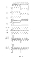
voltage generating circuit 9 comprises a well-known digital-to-analog converter (referred to hereinafter as D/A converter) 91 and a well-known differentiatingcircuit 92 comprising a capacitor and a resistor (neither shown in the figure). D/A converter 92 converts the counted number output from up-down counter 92 into a DC voltage Vd. Differentiatingcircuit 92 generates a spike pulse DP whose amplitude is substantially equal to the DC voltage Vd. The D/A converter 91 is devised so that the output of the D/A converter is limited to in a period which is shorter than the scan selection period but includes the front edge of the output pulse, though not shown in the figures. This spike pulse has the same polarity and same waveform as those of the undesirable spike pulses, induced on the scan electrodes, causing distortions of voltage waveforms applied to the cells. A feedback circuit comprises aninverter 101 which inverts the polarity of the spike pulse DP, and twoadder circuit inverter 101 is input to each of second input terminals of theadder circuits feedback line 102, thus is superposed onto the unselective scan electrode voltages V₂ and V₅. These unselective scan electrode voltages are applied onto all other scan electrodes than the presently selected scan electrode Yi. In synchronization with selecting the present scan electrode Yi, the X data XDi being applied in parallel form to each of data electrodes induces the undesirable spike voltage on the scan electrodes, as described above. Then, the induced undesirable spike voltages are cancelled by the above-described compensation pulse DP′. In a practical circuit, the level of the fed-back compensation pulse may be adjusted, for example, with a variable potentiometer (which is not shown in the figure), while the display panel is visually observed, and fixed. - Voltage waveforms generated in FIG. 1 circuit in displaying a pattern shown in FIG. 4 where a white dot indicates an ON-STATE cell, and a black dot indicates an OFF-STATE cell, are illustrated in FIG. 3, where the first frame is in the positive voltage application mode and the second frame is in the negative voltage application mode. Dotted lines shown there indicate the waveforms before the present invention is embodied thus including the undesirable spike pulse, and the solid lines indicate the waveforms after the present invention is embodied. As observed there, the undesirable spikes induced on the scan electrodes can be cancelled on selecting each of the scan electrodes. With the dotted line waveforms without embodying the present invention, the effective voltage value of the "A" cell voltage (X₁ - Y₁) having spikes extending outwards is larger than the effective voltage value of the "B" cell voltage (X₂ - Y₁) having spikes sinking inwards, thus, the "A" cell was brighter than the "B" cell, that is, a cross-talk is taking place.
- FIG. 5 shows a configuration of the second preferred embodiment of the present invention. The differences of the second preferred embodiment from the first preferred embodiment are in that the
inverter 101 in the first preferred embodiment is omitted in the second preferred embodiment, and four adder circuits 112 - 115 are newly provided in feeder lines of the DC voltage sources V₁ and V₆ selecting the ON-STATE and the DC voltage sources V₃ and V₄ selecting the OFF-STATE, each connected to thedata driver 1 instead of thescan driver 2. Accordingly, the compensation pulse fed back via a feedback line 105 to the data electrodes is of the same waveform having the same polarity and same amplitude as those of the undesirable spikes induced on the unselected scan electrodes. Therefore, the undesirable spike pulse does not appear on the unselected cell voltage being the difference of the data electrode voltage and the scan electrode voltage. Other circuit figurations being the same and performing the same as those of FIG. 2, are denoted with the same numerals, while no more explanation is given for each. - FIG. 6 shows the third preferred embodiment of the present invention. In the third preferred embodiment, in the compensation
voltage generating circuit 9′ the differentiatingcircuit 92 in the FIG. 2 compensationvoltage generating circuit 9 has been deleted. DC output voltage Cp, which is constant during the scan electrode selection period, from the D/A converter 91′ is inverted by aninverter amplifier 101. An output Cp′ of theinverter amplifier 101 is fed back via thefeedback line 102 to the unselected scan electrodes during the period of selecting the present scan electrode Yi. Voltage waveforms to display the pattern of FIG. 4 are illustrated in FIG. 7. According to this configuration, a DC voltage which is effectively equivalent, during the period of selecting a scan electrode, to the undesirable spike voltage is fed back to the source voltages V₂ and V₅. This is because, as described above, the optical transparency of the liquid crystal cell depends on the effective value of the cell voltage. In a practical circuit, the feedback level may be adjusted with a potentiometer (which is not shown in the figure) at an optimum condition while the display panel is visually observed, as described for the first preferred embodiment, and fixed. The circuit configuration of the third preferred embodiment gives an advantageous effect identical to that of the first or the second preferred embodiment while the circuit is simplified by deleting the differentiatingcircuit 92. - Furthermore, though not shown in a figure, a modification is apparently possible that the
inverter 101 is deleted from the circuits of the FIG. 6 third preferred embodiment so that DC compensation voltage is fed back to the power source voltages ofdata driver 1, in the same way as the modification of the first preferred embodiment to the second preferred embodiment. - The fourth preferred embodiment of the present invention is shown in FIG. 8, where the compensation voltage is generated by an analog method instead of the first, second and third preferred embodiments, where the change in the display data is digitally provided by the counter. The fourth preferred embodiment is different from the first preferred embodiment in that the data
difference detecting circuit 8 is replaced with acounter 83 andmemory 7 is deleted. Accordingly, only the portions different from those of FIG. 1 first preferred embodiment are hereinafter described. Other circuits being the same as in FIG. 1 are denoted with the same numerals so as to give no more description thereon.Counter 83 is input with the data synchronizing signal DCLK as a clock signal from thedisplay controller 15, and is input at first with the output XDi-1′ of scan electrodes Yi-1 from thelogic converting circuit 6 at the enable terminal EN. Therefore, logical level "1" output from thelogic converting circuit 6 enables counter 83 to count the data synchronizing signal DCLK.Counter 83 is further provided with a reset terminal RST to which the scan synchronizing signal SSYNC transmitted from thedisplay controller 15 is input so as to initialize the count number, i.e. resets the count number zero, for every scan drive period. Therefore, counter 83 counts quantity of the logic level "1" outputs (representing ON-STATE bits to be displayed on a scan electrode during the positive voltage application mode, as well as representing OFF-STATE bits during the negative voltage application mode) from thelogic converting circuit 6. Compensationvoltage generating circuit 9˝ comprises D/A converter 91′ and differentiatingcircuit 92. D/A converter 91′ converts the count number ofcounter 83 to a DC voltage Vd2. Successively, counter 83 counts the quantity of the logic level "1" in X data XDi′ to be displayed on the next, i.e. present, scan electrode Yi transmitted from thelogic converting circuit 6, and outputs the counted number to the D/A converter 91′ in synchronization with the application of scan electrode voltage to select the present scan electrode Yi. Therefore, upon being input with the newly counted number, the DC output voltage Vd2 of the D/A converter 91′ changes to a new DC voltage corresponding to the newly counted number for the scan electrode Yi. Output voltage Vd2 of the D/A converter 91′ is input to differentiatingcircuit 92, which differentiates the transition of the DC voltages Vd2 so as to output a spike pulse DP₂, which is a compensation signal. Spike pulse DP₂ is inverted by aninverting circuit 101. Amplitude of the spike pulse DP₂′ output from the invertingcircuit 101 is proportional to the change in the DC voltage Vd2 output from the D/A converter 91′, and has the same polarity and the substantially same shape as those of the undesirable spike pulse induced on the unselected scan electrodes. Thus, the amplitude of the compensation signal pulse is proportional to the change in the quantities of the ON-STATE cells on the just previous scan electrode Yi-1 to on the presently selected scan electrode Yi, for the positive voltage application mode, as well as the quantity of OFF-STATE cells for the negative voltage application mode. The compensation signal is fed back to the unselected scan electrodes in the same way as the first preferred embodiment. - Voltage waveforms in the circuit of the fourth preferred embodiment for the display pattern of FIG. 4 are shown in FIGs. 9. In the first frame being in the positive voltage application mode, the quantity of ON-STATE cells on each of the scan electrodes Y₁ ∼ Y₈ is respectively counted as 5, 1, 4, 1, 4, 1, 4 and 1 as seen in the pattern on FIG. 4. And, a DC voltage Vd proportional to each of these numbers is generated. Then, a spike pulse DP₂ having its amplitude proportional to each of the changes in these DC voltages, i.e. the changes -4, 3,-3, 3,-3, 3 and -3, is output from the differentiating
circuit 92. Then, in the same way as that of the first preferred embodiment, spike pulse DP₂ output from the differentiatingcircuit 92 is inverted and superposed onto the unselective scan voltages so as to cancel the undesirable spike pulse induced on the unselected scan electrodes illustrated with dotted lines in the figure. In the second frame being in the negative voltage application mode, the number of OFF-STATE cells on each of the scan electrodes Y₁ ∼ Y₈ is respectively counted. All the other processes are the same as those of the first preferred embodiment. In the practical circuit, the level of the compensation pulse may be adjusted, for example, with a variable potentiometer (which is not shown in the figure), while the display panel is visually observed, and fixed. - The fifth preferred embodiment of the present invention is shown in FIG. 10. Difference of the fifth preferred embodiment from the fourth preferred embodiment is the same as the difference of the second preferred embodiment from the first preferred embodiment. That is, the inverting
circuit 101 has been deleted, and fouradder circuits 112 ∼ 115 are provided on power feeding lines for the DC voltage sources V₁ and V₆ to select the ON-STATE and the DC voltage sources V₃ and V₄ to select the OFF-STATE, to thedata driver 1 instead of thescan driver 2. Accordingly, the compensation pulse DP₂ fed back to the power source circuit has the same polarity and the same amplitude as those of the undesirable spike induced on the unselected scan electrodes. Thus, none of the undesirable spike pulse appears on the cell voltages of the unselected cells. Other circuits being the same as in FIG. 8 are denoted with the same numerals so as to give no description thereon. - The sixth preferred embodiment of the present invention is shown in FIG. 11. In the sixth preferred embodiment the invention is embodied on a
panel 3′ having two screens, divided into an upper screen and a lower screen. Data electrodes for each screen are driven by independent data drivers 1U and 1D, respectively. Scan electrodes of an equal scan order on the upper and lower screens are connected to each other and commonly driven by thesingle scan driver 2. Therefore, the undesirable spike pulse is induced on the unselected scan electrodes of both the screens according to a change in the sum of the quantities of the ON-STATE or OFF-STATE cells displayed on the selected commonly-connected scan electrodes. In the sixth preferred embodiment, for the upper and lower screens 1U and 1D of thepanel 3′, independentlogic converting circuits independent counters circuit 11 composed of a decoder configuration, the compensationvoltage generating circuits 9˝ and the feedback circuit are commonly provided. Thelogic converting circuits voltage generating circuits 9˝ are respectively the same as those in the fourth preferred embodiment shown in FIG. 8. Quantities of the ON-STATE cells during the positive voltage application mode or OFF-STATE cells the negative voltage application mode, to be displayed on the commonly connected scan electrodes are counted respectively for the upper and the lower screens, in the same manner as that of the fourth preferred embodiment. Thus counted quantities are summed by the addingcircuit 11. A DC voltage Vd2 is generated in the D/A converter 91′ in proportion to the summed quantity output from theadder circuit 11. A spike pulse DP₂ is generated in proportion to a change in the generated DC voltages Vd2 by the differentiatingcircuit 92. In the same way as that of the fourth preferred embodiment the spike pulse DP₂ is inverted by theinverter circuit 101 and fed back to the voltage sources of the scan electrodes, so as to cancel the undesirable spike pulses induced on the unselected scan electrodes. - For driving the divided screens, other variations than that shown in the FIG. 11 sixth preferred embodiment are possible as described below though no figures are shown therefor. The concept of the fifth preferred embodiment can be embodied in driving the divided screens. That is, the compensation voltage output from the compensation
voltage generating circuit 9˝ is fed back to each of the data drivers 1U and 1D so that the compensation voltage is superposed onto the data electrode voltages for selecting both the ON-STATE and OFF-STATE in the same polarity of the undesirable spike pulse induced on the unselected scan electrodes. - Any of the above-described concepts of the present invention can be embodied in a circuit configuration where independent plural scan drivers are provided for each of the divided screens. In the plural scan driver configuration the cross-talk caused by the undesirable spikes are independently suppressed on each of divided screens.
- The seventh preferred embodiment shown in FIG. 12, where though in the above-described preferred embodiments the compensation voltage is proportional to the change of the data to be displayed on each scan electrode, the compensation voltage may be adjusted according to a predetermined relation other than the above-described proportional relation. A coversion table 93 composed of a ROM (read only memory) and latch 94 are serially aded between a data
difference counting circuit 60 and D/A converter 91′. The datadifference counting circuit 60 will be described in detail later on, however functions the same as thelogic converting circuit 6, theline memory 7 and the datadifference detecting circuit 8 of the first preferred embodiment shown in FIG. 1. Accordingly, the output of the datadifference counting circuit 60 is a change in the quantity of the logic level "1" data (representing ON-STATE bits to be displayed on a scan electrode during the positive voltage application mode, as well as representing OFF-STATE bits during the negative voltage application mode) from the previous scan electrode Yi-1 into the present scan electrode Yi. The amount of adjustment of the compensation is given in a graph shown in FIG. 13, i.e. the relation of the the above-described change in the counted X data of the presently selected scan electrode Yi from the just prior scan electrode Yi-1 versus a quantity to be input to D/A converter 91.ROM 93 outputs thus adjusted quantity according to the data change quantity input thereto. Thelatch 94 stores the adjusted data serially output from theROM 93, and outputs the corresponding stored data to the D/A converter 91′in synchronization with the scan synchronizing signal SSYNC selecting the present scan electrode Yi. Output from the D/A converter 91′ is processed in the same way as in the third preferred embodiment shown in FIG. 6. Consequently, thus adjusted compensation voltage properly provides better cancellation of the cross-talk on the panel caused from the undesirable spike pulses induced on the unselected scan electrodes. The conversion table shown in FIG. 13 is an example for a particular panel; therefore, the conversion table may be modified depending on the panel and the circuit employed thereto. In a practical circuit, the level of the fed-back compensation voltage may be adjusted, for example, with a variable potentiometer (which is not shown in the figure), while the display panel is visually observed, and fixed. - As is described above, the data
difference counting circuit 60 functions identically to the corresponding circuits of the first preferred embodiment, however, is different in structure as shown in FIG. 12. Constitution and operation of thedata counting circuit 60 are hereinafter described in detail.Inverter 61 and exclusive ORgate 62 are identical to those of the first preferred embodiment, so that, a logical level "1" in the X data XD is output as a logical level "1" from the exclusive OR-gate 62 during a positive voltage application mode. During a negative voltage application mode, a logical level "0" in the X data is output as a logical level "1" from the exclusive ORgate 62. The logical level "1" output from the exclusive ORgate 62 is enabled by an ANDgate 63 with a clock pulse DCLK so as to be input to a down-counter 64 and an up-counter 65, and is down-counted and up-counted respectively therein. It is now assumed that a quantity of ON-STATE bits in X data XDi-1′ for scan electrode Yi-1 during a positive voltage application mode is 30. Then, the count-number counted by the down-counter 64 becomes -30, because the down-counting was started from 0. Prior to starting the counting of data for the present scan electrode Yi, the counted number -30 is input, as an initial number, to the up-counter 65. Next, the up-counter 65 up-counts X data XDi for the next scan electrode Yi from -30. Therefore, if the quantity of ON-STATE bits on scan electrode Yi is 100, the final count number of the up-counter 65 becomes 70. Thus, the up-counter 65 outputs difference of the quantities of the level "1" bits between the just prior scan electrode Yi-1 and the presently selected scan electrode Yi. - Though two types of data counting circuits, i.e. the first type composed of
logic converting circuit 6,line memory 7, datadifference detecting circuit 8 and up-down counter 82 shown in FIG. 1, FIG. 5 and FIG. 6, and the second type denoted with the numeral 60 in FIG. 12, it is apparent that many other circuit constitutions are possible as long as the function is equivalent. - Though the seventh preferred embodiment is described as a variation of the first preferred embodiment, it is apparent that the method of the seventh preferred embodiment may be embodied in other circuits, such as the second and the third preferred embodiments.
- Furthermore, referring to FIG. 14, the eighth preferred embodiment, which is another method and circuit for cancelling the undesirable spikes induced on unselected scan electrodes, is hereinafter described in detail. Difference of the eighth preferred embodiment from the first preferred embodiment is in that the compensation voltage, which is fed back to the scan electrodes so as to cancel the undesirable spike induced on the scan electrodes voltages, is detected from one of the scan electrodes. Accordingly, for the eighth preferred embodiment the
logic converting circuit 6,line memory 7, the datadifference detecting circuit 8 and the compensationvoltage generating circuit 9 have been deleted from the circuit configuration of the FIG. 1 first preferred embodiment, and adistortion detecting circuit 12 is newly added. Selective and unselective voltages applied to the data electrodes and the scan electrodes are identical to those of the first preferred embodiment.Distortion detecting circuit 12 comprises areference driver 121, acomparator 122 and aninverter 101. A first input terminal of thecomparator 122 is connected to one of the scan electrodes, Y₁, as a sampling electrode. Six input terminals of thereference driver 121 are input with the same inputs as those to thescan driver 2, that is, four voltages V₁, V₂, V₅ and V₆, Y data and the mode selecting signal DF. Thereference driver 121 selectively outputs, to a second input terminal of thecomparator 122, a reference voltage VY1′ whose waveform is identical to a voltage to be supplied to the above-described sampling electrode Y₁, that is, 0 or (1-1/a)V volt during a positive voltage application mode, as well as V or (1/a)V volt during a negative voltage application mode. On the other hand, an undesirable spike is induced on the voltage of the sampling electrode Y₁ by a current from the cells connected thereto caused by an application of data voltages from thedata driver 1. Thus, thecomparator 122 compares the voltage VY1 of the sampling electrode Y1 including the undesirable spike with the reference voltage VY1′ output of thereference driver 121 so as to output their difference (VY1 - VY1′), which is a distortion, i.e. the induced spike component. The output from thecomparator 122 is inverted in its polarity by theinverter 101. This inverted signal is a compensation voltage having the same waveform and an opposite polarity to the undesirable spike, and is fed back to the scan driving voltages V₂ and V₅ via theadder circuits comparator 122 may be fed back to thedata driver 1 in the same way as that of the first preferred embodiment. In a practical circuit, the level of the fed-back compensation pulse may adjusted, for example, with a variable potentiometer (which is not shown in the figure), while the display panel is visually observed, and fixed. - Though in the above-described preferred embodiments, an
inverter 101 is provided to feedback the compensation voltage to scan electrodes, the inverter may be deleted when the D/A converter 91, thedifferentiator 92 or thecomparator 122 is of such type that outputs an already inverted compensation voltage onto thefeedback line 102 or 105. - Still furthermore, referring to FIG. 16, the ninth preferred embodiment of the present invention is hereinafter described, which is an improvement of the above-described compensation
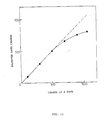
voltage generating circuit power source circuit 4. Thus, each voltage to drive the scan electrodes and the data electrodes is variably set so as to set the cell voltages. An increased brightness control voltage VLCD increases the cell voltage, resulting in an increase in the cell brightness. Contrary, a decreased brightness control voltage VLCD decreases the cell voltage, resulting in a decrease in the cell brightness. However, because of the cross-talk the above-described effect of adjusting the brightness control voltage VLCD is not always equal on the bright cells, as shown in FIG. 17 where curves "A" and "B" represent the optical transparency, i.e. the brightness, of ON-STATE of the cells "A" and "B" shown in FIG. 4 pattern, versus the brightness control voltage VLCD. As seen in FIG. 17, the gradient of the curves are not equal, that is, curve "B" of cell "B" whose brightness is decreased by the cross-talk is less steep than curve "A" of cell "A" whose brightness is increased by the cross-talk. Brightness of the two cells "A" and "B" is equal only at the intersection of two curves "A" and "B", where the brightness control voltage is VLCD1. At the other brightness control voltages than VLCD1, the cross-talk takes place on both the cells "A" and "B". In other words, in the above-described preferred embodiments the cross-talk can be cancelled only when the brightness control voltage is set at VLCD1. - In order to perfectly prevent the above-described cross-talk problem even when the brightness control voltage is varied, in the FIG. 16 ninth preferred embodiment the compensation voltage introduced in the above-described preferred embodiments is adjusted depending on the brightness control voltage as shown in FIG. 18. That is, at a brightness control voltage VLCD3 which is higher than VLCD1 the compensation voltage is adjusted to become larger, and at a brightness control voltage VLCD2 lower than VLCD1 the compensation voltage is adjusted to become lower. Amount of the adjusted compensation voltage ΔV is given by formula:
ΔV = ΔVm K (VLCD1 - Vf)
where ΔVm indicates the compensation voltage before the adjustment, i.e. compensation voltage introduced in the above-described first to eighth preferred embodiments; K indicates a constant; and Vf indicates a predetermined constant voltage which determines the location of the curve V with respect to the brightness control voltage VLCD in FIG. 18. Thus adjusted compensation voltage ΔV adjusts the curves "A" and "B" to have an equal gradient, so that both the cells "A" and "B" have no cross-talk take place thereon, respectively. Circuit configuration for generating this adjusted compensation voltage ΔV is shown typically in FIG. 16. There is provided a potentiometer type variable resistor VR2 whose one of fixed terminals is connected to the brightness control voltage VLCD1 and another fixed terminal is connected to a constant DC voltage source having an output voltage -Vf. The variable terminal outputs a power source voltage to be applied to the D/A converter 91, whose DC output voltage varies in accordance with the applied power source voltage thereto. Thus, the compensation voltage output from the D/A converter is adjusted according to the above described formula. The variable potentiometer which may be employed for adjusting the compensation voltage level in the first to eighth preferred embodiments is unnecessary in the FIG. 16 ninth preferred embodiment. - It is apparent that the FIG. 16 ninth preferred embodiment may be embodied in combination with any of the above-described preferred embodiments, though no drawing nor description is particularly given thereon.
- As is described above, according to the present invention, in driving a direct drive matrix type liquid crystal display, there is provided an advantageous effect in that an undesirable display irregularity caused from cross-talk of data signal onto scan drive voltage can be suppressed, so that the display quality can be improved.
- The many features and advantages of the invention are apparent from the detailed specification and thus, it is intended by the appended claims to cover all such features and advantages of the system which fall within the true spirit and scope of the invention. Further, since numerous modifications and changes may readily occur to those skilled in the art, it is not desired to limit the invention to the exact construction and operation shown and described, and accordingly, all suitable modifications and equivalents may be resorted to, falling within the scope of the invention.
Claims (45)
a plurality of liquid crystal cells arranged in matrix between a plurality of data electrodes and a plurality of scan electrodes, said data electrodes and said scan electrodes intersecting each other, each of said cell being selectively applied with a cell voltage to select ON-STATE or OFF-STATE from said data electrode and scan electrode, polarity of said cell voltage to select said ON-STATE being altered in a predetermined period, wherein
a compensation voltage is generated according to a predetermined relation to a change in a first quantity of data bits, having a first logical level, displayed on a just previous scan electrode into a second quantity of data bits, having said first logical level, to be displayed on a present scan electrode, when said cells being driven with a voltage in a first polarity, or according to said predetermined relation to a change in a first quantity of data bits, having a second logical level opposite to said first logical level, to be displayed on a first scan electrode into a second quantity of data bits, having said second logical level, to be displayed on the next scan electrode; and
said compensation voltage is superposed on voltages driving unselected scan electrodes in a polarity opposite to a spike voltage induced on said unselected scan electrodes by an application of voltages driving said data electrodes, in synchronization with selection of said present scan electrode.
counting a third quantity of data bits changing from said second logical level to said first logical level;
counting a fourth quantity of data bits changing from said second logical level to said first logical level; and
reducing said fourth quantity from said third quantity.
a plurality of liquid crystal cells arranged in matrix between a plurality of data electrodes and a plurality of scan electrodes, said data electrodes and said scan electrodes intersecting each other, each of said cell being selectively applied with a cell voltage to select ON-STATE or OFF-STATE from said data electrode and scan electrode, polarity of said cell voltage to select said ON-STATE being altered in a predetermined period, wherein
a compensation voltage is generated according to a predetermined relation to a change in a first quantity of data bits, having a first logical level, displayed on a just previous scan electrode to a second quantity of data bits, having said first logical level, to be displayed on a present scan electrode, when said cells being driven with a voltage in a first polarity, or according to said predetermined relation to a change in a first quantity of data bits, having a second logical level opposite to said first logical level, to be displayed on a first scan electrode into a second quantity of data bits, having said second logical level, to be displayed on the next scan electrode; and
said compensation voltage is superposed on each of voltages driving said data electrodes in the same polarity as a spike voltage induced on said unselected scan electrodes by an application of voltages driving said data electrodes, in synchronization with selection of said present scan electrode.
counting a third quantity of data bits changing from said second logical level to said first logical level;
counting a fourth quantity of data bits changing from said second logical level to said first logical level; and
reducing said fourth quantity from said third quantity.
a panel having a plurality of liquid crystal cells arranged, in matrix, between a plurality of data electrodes and a plurality of scan electrodes, said data electrodes and said scan electrodes intersecting each other, ON-STATE and OFF-STATE of each cell being determined by cell voltage which is a difference between voltages of data electrode and scan electrode respectively connected said each cell, cell voltage to select ON-STATE being in a first polarity during a first voltage application mode, cell voltage to select ON-STATE being in a second polarity opposite to said first polarity during a second voltage application mode;
mode selecting means for outputting a mode selecting signal which selects said voltage application mode, so as to switch said voltage application mode in a predetermined cycle;
power sources for outputting selective voltages to select ON-STATE for the first and second voltage application modes, respectively, and unselective voltages to select OFF-STATE for said first and second modes, respectively;
a scan driver, for selectively applying said selective and unselective voltages output from said power source to each of said scan electrodes, said selective and unselective voltages being selected depending on said mode selecting signal;
a data driver for selectively applying said selective and unselective voltages output from said power source to each of said data electrodes, said selective and unselective voltages being selected depending on said mode selecting signal;
logic converting means for converting a first logical level in data to be displayed on a scan electrode into a second logical level opposite to said first logical level during said first voltage application mode, and converting a second logical level in said data into said first logical level during said second voltage application mode;
data difference detecting means for reducing a first quantity of logical level 1 output from said logic converting means displayed on a just previous scan electrode from a second quantity of logical level 1 output from said logic converting means to be displayed on a present scan electrode;
compensation voltage generating means for generating a compensation voltage having a level in accordance to a predetermined relation to a change output from said data difference detecting means; and
feedback means for superposing said compensation voltage onto voltages to be supplied via said scan driver to other unselected scan electrodes than said next scan electrode in synchronization with selection of said present scan electrode, so as to cancel undesirable spike pulse induced on said unselected scan electrodes on an application of selective and unselective voltages onto each data electrode.
memory means for storing an output of said logic converting means during a period selecting a single scan electrode; and
data change detecting means for reducing a third quantity of bits changing from logic level 1 to logic level 0 from a fourth quantity of bits changing from logic level 0 to logic level 1, in comparing each of corresponding bits of an output from said logic converting means outputting a data to be displayed on said present scan electrode and an output from said memory means outputting a data displayed on previous scan electrode.
a panel having a plurality of liquid crystal cells arranged, in matrix, between a plurality of data electrodes and a plurality of scan electrodes, said data electrodes and said scan electrodes intersecting each other, ON-STATE and OFF-STATE of each cell being determined by cell voltage which is a difference between voltages of data electrode and scan electrode respectively connected said each cell, cell voltage to select ON-STATE being in a first polarity during a first voltage application mode, cell voltage to select ON-STATE being in a second polarity opposite to said first polarity during a second voltage application mode;
mode selecting means for outputting a mode selecting signal which selects said voltage application mode, so as to switch said voltage application mode in a predetermined cycle;
power sources for supplying selective voltages to select ON-STATE for the first and second voltage application modes, respectively, and unselective voltages to select OFF-STATE for said first and second modes, respectively;
a scan driver, for selectively applying said selective and unselective voltages output from said power source to each of said scan electrodes, said selective and unselective voltages being selected depending on said mode selecting signal;
a data driver for selectively applying said selective and unselective voltages output from said power source to each of said data electrodes, said selective and unselective voltages being selected depending on said mode selecting signal;
logic converting means for converting a first logical level in data to be displayed on a scan electrode into a second logical level opposite to said first logical level during said first voltage application mode, and converting a second logical level in said data into said first logical level during said second voltage application mode;
data difference detecting means for reducing a first quantity of logical level 1 output from said logic converting means displayed on a just previous scan electrode from a second quantity of logical level 1 output from said logic converting means to be displayed on a present scan electrode;
compensation voltage generating means for generating a compensation voltage having a level in accordance to a predetermined relation to a change output from said data difference detecting means; and
feedback means for superposing said compensation voltage onto voltages to be supplied via said data driver to each of said data electrodes in synchronization with selection of said present scan electrode, so as to cancel undesirable spike pulse induced on said unselected scan electrodes on an application of selective and unselective voltages onto each data electrode.
memory means for storing an output of said logic converting means during a period selecting a single scan electrode; and
data change detecting means for reducing a third quantity of bits changing from logic level 1 to logic level 0 from a fourth quantity of bits changing from logic level 0 to logic level 1, in comparing each of corresponding bits of an output from said logic converting means outputting a data to be displayed on said present scan electrode and an output from said memory means outputting a data displayed on previous scan electrode.
a plurality of liquid crystal cells arranged in matrix between a plurality of data electrodes and a plurality of scan electrodes, said data electrodes and said scan electrodes intersecting each other, each of said cell being selectively applied with a cell voltage to select ON-STATE or OFF-STATE from said data electrode and scan electrode, wherein
a spike voltage induced on one of said scan electrodes by an application of voltages to drive said data electrodes is superposed on voltages to drive unselected scan electrodes, in a polarity opposite to said spike voltage on said unselected scan electrodes, so as to cancel said spike voltage.
a plurality of liquid crystal cells arranged in matrix between a plurality of data electrodes and a plurality of scan electrodes, said data electrodes and said scan electrodes intersecting each other, each of said cell being selectively applied with a cell voltage to select ON-STATE or OFF-STATE from said data electrode and scan electrode, wherein
a spike voltage induced on one of said scan electrodes by an application of voltages to drive said data electrodes is superposed on voltages to drive said data electrodes, in a polarity same as said spike voltage on said unselected scan electrodes, so as to cancel said spike voltage.
a panel having a plurality of liquid crystal cells arranged, in matrix, between a plurality of data electrodes and a plurality of scan electrodes, said data electrodes and said scan electrodes intersecting each other;
a data driver connected to each of said data electrodes, for applying selective and unselective voltages to each of said data electrodes;
a scan driver connected to each of said scan electrodes, for applying selective and unselective voltages to each of said scan electrodes;
power sources for supplying each of said selective and unselective voltage to said data driver and said scan driver; and
detecting means connected to one of said scan electrodes as a sample scan electrode, for detecting a spike voltage induced on said sample scan electrode, and outputting a compensation voltage in an opposite polarity to said spike voltage;
feedback means for superposing said compensation voltage onto voltages to be applied to unselected scan electrodes from said power sources.
said detecting means comprises: reference means outputting the same voltage as said voltage to be applied to said sample scan electrodes as a reference voltage; reduction means for outputting a reduction of said reference voltage from a voltage of said sample scan electrode; and inverting means for inverting polarity of said reduction; and
said feedback means comprises adder circuits for adding an output of said detecting means to unselective voltages to be supplied to said unselected scan electrodes.
said power sources provides selective and unselective voltages to be supplied to data electrodes and scan electrodes, both for positive and negative voltage application modes, where said positive voltage application mode is such that a cell is selected by a positive cell voltage with respect to data electrode potential and said negative voltage application mode is such that a cell is selected by a negative cell voltage with respect to data electrode potential; and
mode switching means is further comprised, for switching said voltage application modes in a predetermined cycle.
a panel having a plurality of liquid crystal cells arranged, in matrix, between a plurality of data electrodes and a plurality of scan electrodes, said data electrodes and said scan electrodes intersecting each other;
a data driver connected to each of said data electrodes, for applying selective and unselective voltages to each of said data electrodes;
a scan electrodes connected to each of said scan electrodes, for applying selective and unselective voltages to each of said scan electrodes;
power sources for supplying each of said selective and unselective voltage to said data driver and said scan driver; and
detecting means connected to one of said scan electrodes as a sample scan electrode, for detecting a spike voltage induced on said sample scan electrode, and outputting a compensation voltage in the same polarity as said spike voltage;
feedback means for superposing said compensation voltage onto voltages to be applied to each of data electrodes from said power sources.
said detecting means comprises: reference means outputting the same voltage as said voltage to be applied to said sample scan electrodes as a reference voltage; reduction means for outputting a reduction of said reference voltage from a voltage of said sample scan electrode; and inverting means for inverting polarity of said reduction; and
said feedback means comprises adder circuits for adding an output of said detecting means to voltages to be supplied to each of said data electrodes.
said power sources provides selective and unselective voltages to be supplied to data electrodes and scan electrodes, both for positive and negative voltage application modes, where said positive voltage application mode is such that a cell is selected by a positive cell voltage with respect to data electrode potential and said negative voltage application mode is such that a cell is selected by a negative cell voltage with respect to data electrode potential; and
mode switching means for switching said voltage application modes in a predetermined cycle is further comprised.
a plurality of liquid crystal cells arranged in matrix between a plurality of data electrodes and a plurality of scan electrodes, said data electrodes and said scan electrodes intersecting each other, each of said cell being selectively applied with a cell voltage to select ON-STATE or OFF-STATE from said data electrode and scan electrode, wherein
a compensation voltage is generated according to a predetermined relation to a change in a first quantity of data bits, having a first logical level representing said ON-STATE of said OFF-STATE, displayed on a just previous scan electrode into a second quantity of data bits, having said first logical level, to be displayed on a present scan electrode; and
said compensation voltage is superposed on voltages driving unselected scan electrodes in a polarity opposite to a spike voltage induced on said unselected scan electrodes by an application of voltages driving said data electrodes, in synchronization with selection of said present scan electrode.
Applications Claiming Priority (8)
| Application Number | Priority Date | Filing Date | Title |
|---|---|---|---|
| JP32728788A JPH02171718A (en) | 1988-12-23 | 1988-12-23 | Method and device for driving liquid crystal display panel |
| JP327287/88 | 1988-12-23 | ||
| JP33147788A JPH02178623A (en) | 1988-12-29 | 1988-12-29 | Method and device for driving liquid crystal display device |
| JP331477/88 | 1988-12-29 | ||
| JP36977/89 | 1989-02-15 | ||
| JP3697789A JP2503265B2 (en) | 1989-02-15 | 1989-02-15 | Driving method of liquid crystal display device |
| JP15753589A JPH0833713B2 (en) | 1989-06-19 | 1989-06-19 | Driving method for liquid crystal display device |
| JP157535/89 | 1989-06-19 |
Publications (3)
| Publication Number | Publication Date |
|---|---|
| EP0374845A2 true EP0374845A2 (en) | 1990-06-27 |
| EP0374845A3 EP0374845A3 (en) | 1991-02-13 |
| EP0374845B1 EP0374845B1 (en) | 1995-04-12 |
Family
ID=27460348
Family Applications (1)
| Application Number | Title | Priority Date | Filing Date |
|---|---|---|---|
| EP89123476A Expired - Lifetime EP0374845B1 (en) | 1988-12-23 | 1989-12-19 | Method and apparatus for driving a liquid crystal display panel |
Country Status (4)
| Country | Link |
|---|---|
| US (1) | US5307084A (en) |
| EP (1) | EP0374845B1 (en) |
| CA (1) | CA2006070C (en) |
| DE (1) | DE68922197T2 (en) |
Cited By (10)
| Publication number | Priority date | Publication date | Assignee | Title |
|---|---|---|---|---|
| EP0431628A2 (en) * | 1989-12-07 | 1991-06-12 | Seiko Epson Corporation | Liquid crystal display device |
| EP0466506A2 (en) * | 1990-07-13 | 1992-01-15 | Citizen Watch Co., Ltd. | Electrooptical display device |
| EP0542307A2 (en) * | 1991-11-15 | 1993-05-19 | Asahi Glass Company Ltd. | Image display device and a method of driving the same |
| US5214417A (en) * | 1987-08-13 | 1993-05-25 | Seiko Epson Corporation | Liquid crystal display device |
| WO1995013603A1 (en) * | 1993-11-12 | 1995-05-18 | In Focus Systems, Inc. | Passive matrix display having reduced image-degrading crosstalk effects |
| US5473338A (en) * | 1993-06-16 | 1995-12-05 | In Focus Systems, Inc. | Addressing method and system having minimal crosstalk effects |
| US5583528A (en) * | 1990-07-13 | 1996-12-10 | Citizen Watch Co., Ltd. | Electrooptical display device |
| US5670973A (en) * | 1993-04-05 | 1997-09-23 | Cirrus Logic, Inc. | Method and apparatus for compensating crosstalk in liquid crystal displays |
| SG111019A1 (en) * | 2000-07-24 | 2005-05-30 | Seiko Epson Corp | Driving method for electro-optical apparatus, driving circuit therefor, electro-optical apparatus, and electronic equipment |
| DE102005030337B4 (en) * | 2004-06-30 | 2015-09-17 | Lg Display Co., Ltd. | Liquid crystal display and driving method for this |
Families Citing this family (28)
| Publication number | Priority date | Publication date | Assignee | Title |
|---|---|---|---|---|
| US5828354A (en) * | 1990-07-13 | 1998-10-27 | Citizen Watch Co., Ltd. | Electrooptical display device |
| US5841416A (en) * | 1991-04-02 | 1998-11-24 | Hitachi, Ltd. | Method of and apparatus for driving liquid-crystal display device |
| US5434588A (en) * | 1993-12-21 | 1995-07-18 | Motorola, Inc. | Device for minimizing crosstalk in multiplexed addressing signals for an RMS-responding device |
| TW280901B (en) * | 1994-04-19 | 1996-07-11 | Matsushita Electric Ind Co Ltd | |
| JP3107980B2 (en) * | 1994-09-29 | 2000-11-13 | シャープ株式会社 | Liquid crystal display |
| JPH08106272A (en) * | 1994-10-03 | 1996-04-23 | Semiconductor Energy Lab Co Ltd | Display device driving circuit |
| US5640173A (en) * | 1995-03-21 | 1997-06-17 | In Focus Systems, Inc. | Methods and systems for detecting and correcting dynamic crosstalk effects appearing in moving display patterns |
| US5710571A (en) * | 1995-11-13 | 1998-01-20 | Industrial Technology Research Institute | Non-overlapped scanning for a liquid crystal display |
| US7385574B1 (en) * | 1995-12-29 | 2008-06-10 | Cree, Inc. | True color flat panel display module |
| US5790083A (en) * | 1996-04-10 | 1998-08-04 | Neomagic Corp. | Programmable burst of line-clock pulses during vertical retrace to reduce flicker and charge build-up on passive LCD display panels during simultaneous LCD and CRT display |
| JPH09281931A (en) * | 1996-04-10 | 1997-10-31 | Fujitsu Ltd | Display device and circuit and method for driving it |
| US6295042B1 (en) * | 1996-06-05 | 2001-09-25 | Canon Kabushiki Kaisha | Display apparatus |
| KR100632713B1 (en) * | 1997-07-22 | 2006-10-13 | 코닌클리케 필립스 일렉트로닉스 엔.브이. | Display device |
| JP3335560B2 (en) * | 1997-08-01 | 2002-10-21 | シャープ株式会社 | Liquid crystal display device and driving method of liquid crystal display device |
| US6111555A (en) * | 1998-02-12 | 2000-08-29 | Photonics Systems, Inc. | System and method for driving a flat panel display and associated driver circuit |
| JP2000221468A (en) * | 1999-01-29 | 2000-08-11 | Citizen Watch Co Ltd | Liquid crystal drive device |
| WO2001053882A1 (en) * | 2000-01-21 | 2001-07-26 | Citizen Watch Co., Ltd. | Driving method of liquid crystal display panel and liquid crystal display device |
| JP3899817B2 (en) * | 2000-12-28 | 2007-03-28 | セイコーエプソン株式会社 | Liquid crystal display device and electronic device |
| CN1265338C (en) * | 2001-11-21 | 2006-07-19 | 佳能株式会社 | Display device, image signal controller and driving controller thereof |
| TW588183B (en) * | 2002-06-07 | 2004-05-21 | Hannstar Display Corp | A method and an apparatus for decreasing flicker of a liquid crystal display |
| JP2004101581A (en) * | 2002-09-04 | 2004-04-02 | Koninkl Philips Electronics Nv | Image display device |
| US20040085332A1 (en) * | 2002-10-28 | 2004-05-06 | Rohm Co., Ltd. | Display driving method and display device |
| JP2005025798A (en) * | 2003-06-30 | 2005-01-27 | Toshiba Corp | Level detection circuit, phase change detection circuit and optical disk drive |
| JP4401802B2 (en) * | 2004-02-04 | 2010-01-20 | キヤノン株式会社 | camera |
| JP4876610B2 (en) * | 2006-02-14 | 2012-02-15 | セイコーエプソン株式会社 | Image display system, image display method, image display program, recording medium, data processing apparatus |
| US7768490B2 (en) * | 2006-07-28 | 2010-08-03 | Chunghwa Picture Tubes, Ltd. | Common voltage compensation device, liquid crystal display, and driving method thereof |
| KR101318372B1 (en) * | 2006-08-03 | 2013-10-16 | 삼성디스플레이 주식회사 | Illuminant unit, backlight assembly and display apparatus having the same |
| US20080170209A1 (en) * | 2007-01-12 | 2008-07-17 | Seiko Epson Corporation | Image Display System, Image Output System, and Image Display Method |
Citations (7)
| Publication number | Priority date | Publication date | Assignee | Title |
|---|---|---|---|---|
| JPS59210421A (en) * | 1983-05-13 | 1984-11-29 | Seiko Epson Corp | Driving method of matrix type liquid crystal panel |
| US4640582A (en) * | 1983-05-10 | 1987-02-03 | Kabushiki Kaisha Seiko Epson | System for driving a liquid crystal matrix display so as to avoid crosstalk |
| JPS62264029A (en) * | 1986-05-12 | 1987-11-17 | Canon Inc | Driving method for ferroelectric liquid crystal element |
| JPS63220228A (en) * | 1987-03-10 | 1988-09-13 | Casio Comput Co Ltd | Liquid crystal driving system |
| JPS63240528A (en) * | 1987-03-27 | 1988-10-06 | Matsushita Electric Ind Co Ltd | Method for driving liquid crystal panel |
| EP0288168A2 (en) * | 1987-03-31 | 1988-10-26 | Canon Kabushiki Kaisha | Display device |
| FR2615993A1 (en) * | 1987-06-01 | 1988-12-02 | Gen Electric | METHOD AND DEVICE FOR THE ELIMINATION OF COUPLING IN MATRIX ADDRESSED THIN FILM TRANSISTOR LIQUID CRYSTAL SCREENS |
Family Cites Families (8)
| Publication number | Priority date | Publication date | Assignee | Title |
|---|---|---|---|---|
| US3955187A (en) * | 1974-04-01 | 1976-05-04 | General Electric Company | Proportioning the address and data signals in a r.m.s. responsive display device matrix to obtain zero cross-talk and maximum contrast |
| JPS57204592A (en) * | 1981-06-11 | 1982-12-15 | Sony Corp | Two-dimensional address device |
| US4613854A (en) * | 1983-08-22 | 1986-09-23 | Burroughs Corporation | System for operating a dot matrix display panel to prevent crosstalk |
| KR910001848B1 (en) * | 1986-02-06 | 1991-03-28 | 세이꼬 엡슨 가부시끼가이샤 | Liquid crystal displayy |
| NL8602698A (en) * | 1986-10-28 | 1988-05-16 | Philips Nv | METHOD FOR CONTROLLING A DISPLAY DEVICE AND A DISPLAY DEVICE SUITABLE FOR SUCH A METHOD |
| JPS63298287A (en) * | 1987-05-29 | 1988-12-06 | シャープ株式会社 | Liquid crystal display device |
| JP2906057B2 (en) * | 1987-08-13 | 1999-06-14 | セイコーエプソン株式会社 | Liquid crystal display |
| US4845482A (en) * | 1987-10-30 | 1989-07-04 | International Business Machines Corporation | Method for eliminating crosstalk in a thin film transistor/liquid crystal display |
-
1989
- 1989-12-19 EP EP89123476A patent/EP0374845B1/en not_active Expired - Lifetime
- 1989-12-19 DE DE68922197T patent/DE68922197T2/en not_active Expired - Fee Related
- 1989-12-20 CA CA002006070A patent/CA2006070C/en not_active Expired - Fee Related
-
1992
- 1992-04-03 US US07/863,379 patent/US5307084A/en not_active Expired - Fee Related
Patent Citations (7)
| Publication number | Priority date | Publication date | Assignee | Title |
|---|---|---|---|---|
| US4640582A (en) * | 1983-05-10 | 1987-02-03 | Kabushiki Kaisha Seiko Epson | System for driving a liquid crystal matrix display so as to avoid crosstalk |
| JPS59210421A (en) * | 1983-05-13 | 1984-11-29 | Seiko Epson Corp | Driving method of matrix type liquid crystal panel |
| JPS62264029A (en) * | 1986-05-12 | 1987-11-17 | Canon Inc | Driving method for ferroelectric liquid crystal element |
| JPS63220228A (en) * | 1987-03-10 | 1988-09-13 | Casio Comput Co Ltd | Liquid crystal driving system |
| JPS63240528A (en) * | 1987-03-27 | 1988-10-06 | Matsushita Electric Ind Co Ltd | Method for driving liquid crystal panel |
| EP0288168A2 (en) * | 1987-03-31 | 1988-10-26 | Canon Kabushiki Kaisha | Display device |
| FR2615993A1 (en) * | 1987-06-01 | 1988-12-02 | Gen Electric | METHOD AND DEVICE FOR THE ELIMINATION OF COUPLING IN MATRIX ADDRESSED THIN FILM TRANSISTOR LIQUID CRYSTAL SCREENS |
Non-Patent Citations (4)
| Title |
|---|
| PATENT ABSTRACTS OF JAPAN vol. 12, no. 144 (P-697), 6 May 1988; & JP-A-62264029 (CANON) 17.11.1987 * |
| PATENT ABSTRACTS OF JAPAN vol. 13, no. 12 (P-812)(3360), 12 January 1989; & JP-A-63220228 (CASIO COMPUT CO. LTD.) 13.09.1988 * |
| PATENT ABSTRACTS OF JAPAN vol. 13, no. 47 (P-822), 3 February 1988; & JP-A-63240528 (MATSUSHITA ELECTRIC IND.) 06.10.1988 * |
| PATENT ABSTRACTS OF JAPAN vol. 9, no. 79 (P-347), 9 April 1985; & JP-A-59210421 (EPUSON K.K.) 29.11.1984 * |
Cited By (15)
| Publication number | Priority date | Publication date | Assignee | Title |
|---|---|---|---|---|
| US5214417A (en) * | 1987-08-13 | 1993-05-25 | Seiko Epson Corporation | Liquid crystal display device |
| EP0431628A3 (en) * | 1989-12-07 | 1992-06-03 | Seiko Epson Corporation | Liquid crystal display device |
| EP0431628A2 (en) * | 1989-12-07 | 1991-06-12 | Seiko Epson Corporation | Liquid crystal display device |
| US5583528A (en) * | 1990-07-13 | 1996-12-10 | Citizen Watch Co., Ltd. | Electrooptical display device |
| EP0466506A2 (en) * | 1990-07-13 | 1992-01-15 | Citizen Watch Co., Ltd. | Electrooptical display device |
| EP0466506A3 (en) * | 1990-07-13 | 1993-04-21 | Citizen Watch Co. Ltd. | Electrooptical display device |
| US5841412A (en) * | 1990-07-13 | 1998-11-24 | Citizen Watch Co., Ltd. | Electrooptical display device |
| EP0542307A3 (en) * | 1991-11-15 | 1993-08-18 | Asahi Glass Company Ltd. | Image display device and a method of driving the same |
| EP0542307A2 (en) * | 1991-11-15 | 1993-05-19 | Asahi Glass Company Ltd. | Image display device and a method of driving the same |
| US5670973A (en) * | 1993-04-05 | 1997-09-23 | Cirrus Logic, Inc. | Method and apparatus for compensating crosstalk in liquid crystal displays |
| US5473338A (en) * | 1993-06-16 | 1995-12-05 | In Focus Systems, Inc. | Addressing method and system having minimal crosstalk effects |
| US5440322A (en) * | 1993-11-12 | 1995-08-08 | In Focus Systems, Inc. | Passive matrix display having reduced image-degrading crosstalk effects |
| WO1995013603A1 (en) * | 1993-11-12 | 1995-05-18 | In Focus Systems, Inc. | Passive matrix display having reduced image-degrading crosstalk effects |
| SG111019A1 (en) * | 2000-07-24 | 2005-05-30 | Seiko Epson Corp | Driving method for electro-optical apparatus, driving circuit therefor, electro-optical apparatus, and electronic equipment |
| DE102005030337B4 (en) * | 2004-06-30 | 2015-09-17 | Lg Display Co., Ltd. | Liquid crystal display and driving method for this |
Also Published As
| Publication number | Publication date |
|---|---|
| DE68922197D1 (en) | 1995-05-18 |
| DE68922197T2 (en) | 1995-08-10 |
| CA2006070C (en) | 1995-01-24 |
| EP0374845B1 (en) | 1995-04-12 |
| EP0374845A3 (en) | 1991-02-13 |
| US5307084A (en) | 1994-04-26 |
| CA2006070A1 (en) | 1990-06-23 |
Similar Documents
| Publication | Publication Date | Title |
|---|---|---|
| EP0374845B1 (en) | Method and apparatus for driving a liquid crystal display panel | |
| KR920009028B1 (en) | Liquid crystal display device | |
| EP0314084B1 (en) | Driving apparatus | |
| JP3367808B2 (en) | Display panel driving method and apparatus | |
| US5438342A (en) | Liquid crystal display apparatus and method and apparatus for driving same | |
| KR100220959B1 (en) | Liquid crystal driving method and liquid crystal display device | |
| EP0767449A2 (en) | Method and circuit for driving active matrix liquid crystal panel with control of the average driving voltage | |
| JPH0968689A (en) | Driving method of liquid crystal display device | |
| US6172662B1 (en) | Method of driving liquid crystal display device, a liquid crystal display, electronic equipment and a driving circuit | |
| JP2004020657A5 (en) | ||
| US6597335B2 (en) | Liquid crystal display device and method for driving the same | |
| JP2685609B2 (en) | Display device drive circuit | |
| KR100329538B1 (en) | Method and apparatus for driving liquid crystal display panel | |
| US6297786B1 (en) | Liquid crystal display apparatus | |
| JP3674059B2 (en) | Liquid crystal display | |
| US6091387A (en) | Liquid crystal display device and driving method of the same | |
| US5841416A (en) | Method of and apparatus for driving liquid-crystal display device | |
| US6850251B1 (en) | Control circuit and control method for display device | |
| JPH05265402A (en) | Method and device for driving liquid crystal display device | |
| JP2621161B2 (en) | LCD drive system | |
| JPH09198012A (en) | Liquid crystal display device | |
| JPH07114001A (en) | Liquid crystal display device | |
| JP3066221B2 (en) | Simple matrix drive type liquid crystal display | |
| JPH0619428A (en) | Driving system of matrix display device | |
| JP3020228B2 (en) | Liquid crystal display |
Legal Events
| Date | Code | Title | Description |
|---|---|---|---|
| PUAI | Public reference made under article 153(3) epc to a published international application that has entered the european phase |
Free format text: ORIGINAL CODE: 0009012 |
|
| AK | Designated contracting states |
Kind code of ref document: A2 Designated state(s): DE FR GB IT NL |
|
| PUAL | Search report despatched |
Free format text: ORIGINAL CODE: 0009013 |
|
| AK | Designated contracting states |
Kind code of ref document: A3 Designated state(s): DE FR GB IT NL |
|
| 17P | Request for examination filed |
Effective date: 19910302 |
|
| 17Q | First examination report despatched |
Effective date: 19930215 |
|
| GRAA | (expected) grant |
Free format text: ORIGINAL CODE: 0009210 |
|
| AK | Designated contracting states |
Kind code of ref document: B1 Designated state(s): DE FR GB IT NL |
|
| REF | Corresponds to: |
Ref document number: 68922197 Country of ref document: DE Date of ref document: 19950518 |
|
| ITF | It: translation for a ep patent filed |
Owner name: STUDIO JAUMANN |
|
| ET | Fr: translation filed | ||
| PLBE | No opposition filed within time limit |
Free format text: ORIGINAL CODE: 0009261 |
|
| STAA | Information on the status of an ep patent application or granted ep patent |
Free format text: STATUS: NO OPPOSITION FILED WITHIN TIME LIMIT |
|
| 26N | No opposition filed | ||
| PGFP | Annual fee paid to national office [announced via postgrant information from national office to epo] |
Ref country code: DE Payment date: 20001211 Year of fee payment: 12 |
|
| PGFP | Annual fee paid to national office [announced via postgrant information from national office to epo] |
Ref country code: FR Payment date: 20001212 Year of fee payment: 12 |
|
| PGFP | Annual fee paid to national office [announced via postgrant information from national office to epo] |
Ref country code: GB Payment date: 20001213 Year of fee payment: 12 |
|
| PGFP | Annual fee paid to national office [announced via postgrant information from national office to epo] |
Ref country code: NL Payment date: 20001231 Year of fee payment: 12 |
|
| PG25 | Lapsed in a contracting state [announced via postgrant information from national office to epo] |
Ref country code: GB Free format text: LAPSE BECAUSE OF NON-PAYMENT OF DUE FEES Effective date: 20011219 |
|
| REG | Reference to a national code |
Ref country code: GB Ref legal event code: IF02 |
|
| PG25 | Lapsed in a contracting state [announced via postgrant information from national office to epo] |
Ref country code: NL Free format text: LAPSE BECAUSE OF NON-PAYMENT OF DUE FEES Effective date: 20020701 |
|
| PG25 | Lapsed in a contracting state [announced via postgrant information from national office to epo] |
Ref country code: DE Free format text: LAPSE BECAUSE OF NON-PAYMENT OF DUE FEES Effective date: 20020702 |
|
| GBPC | Gb: european patent ceased through non-payment of renewal fee |
Effective date: 20011219 |
|
| PG25 | Lapsed in a contracting state [announced via postgrant information from national office to epo] |
Ref country code: FR Free format text: LAPSE BECAUSE OF NON-PAYMENT OF DUE FEES Effective date: 20020830 |
|
| NLV4 | Nl: lapsed or anulled due to non-payment of the annual fee |
Effective date: 20020701 |
|
| REG | Reference to a national code |
Ref country code: FR Ref legal event code: ST |
|
| PG25 | Lapsed in a contracting state [announced via postgrant information from national office to epo] |
Ref country code: IT Free format text: LAPSE BECAUSE OF NON-PAYMENT OF DUE FEES;WARNING: LAPSES OF ITALIAN PATENTS WITH EFFECTIVE DATE BEFORE 2007 MAY HAVE OCCURRED AT ANY TIME BEFORE 2007. THE CORRECT EFFECTIVE DATE MAY BE DIFFERENT FROM THE ONE RECORDED. Effective date: 20051219 |